Embed Size (px)
Citation preview

SANDIA REPORTSAND2000-2882Unlimited ReleasePrinted November 2000
Optical Interconnections to FocalPlane Arrays
Jeffrey L. Rienstra and Michael K. Hinckley
Prepared bySandia National LaboratoriesAlbuquerque, New Mexico 87185 and Livermore, California 94550
Sandia is a multiprogram laboratory operated by Sandia Corporation,a Lockheed Martin Company, for the United States Department ofEnergy under Contract DE-AC04-94AL85000.
Approved for public release; further dissemination unlimited.

2
Issued by Sandia National Laboratories, operated for the United States Departmentof Energy by Sandia Corporation.
NOTICE: This report was prepared as an account of work sponsored by an agencyof the United States Government. Neither the United States Government, nor anyagency thereof, nor any of their employees, nor any of their contractors,subcontractors, or their employees, make any warranty, express or implied, or assumeany legal liability or responsibility for the accuracy, completeness, or usefulness of anyinformation, apparatus, product, or process disclosed, or represent that its use wouldnot infringe privately owned rights. Reference herein to any specific commercialproduct, process, or service by trade name, trademark, manufacturer, or otherwise,does not necessarily constitute or imply its endorsement, recommendation, or favoringby the United States Government, any agency thereof, or any of their contractors orsubcontractors. The views and opinions expressed herein do not necessarily state orreflect those of the United States Government, any agency thereof, or any of theircontractors.
Printed in the United States of America. This report has been reproduced directlyfrom the best available copy.
Available to DOE and DOE contractors fromU.S. Department of EnergyOffice of Scientific and Technical InformationP.O. Box 62Oak Ridge, TN 37831
Telephone: (865)576-8401Facsimile: (865)576-5728E-Mail: [email protected] ordering: http://www.doe.gov/bridge
Available to the public fromU.S. Department of CommerceNational Technical Information Service5285 Port Royal RdSpringfield, VA 22161
Telephone: (800)553-6847Facsimile: (703)605-6900E-Mail: [email protected] order: http://www.ntis.gov/ordering.htm

3
SAND2000-2882Unlimited Release
Printed November 2000
Optical Interconnections to Focal Plane Arrays
Jeffrey L. Rienstra and Michael K. HinckleySpace Sensor Engineering Department
Sandia National LaboratoriesP.O. Box 5800
Albuquerque, New Mexico 87185-0972
Abstract
We have successfully demonstrated an optical data interconnection from theoutput of a focal plane array to the downstream data acquisition electronics. Thedemonstrated approach included a continuous wave laser beam directed at amultiple quantum well reflectance modulator connected to the focal plane arrayanalog output. The output waveform from the optical interconnect was observedon an oscilloscope to be a replica of the input signal. We fed the output of theoptical data link to the same data acquisition system used to characterize focalplane array performance. Measurements of the signal to noise ratio at the inputand output of the optical interconnection showed that the signal to noise ratio wasreduced by a factor of 10 or more. Analysis of the noise and link gain showedthat the primary contributors to the additional noise were laser intensity noise andphotodetector receiver noise. Subsequent efforts should be able to reduce thesenoise sources considerably and should result in substantially improved signal tonoise performance. We also observed significant photocurrent generation in thereflectance modulator that imposes a current load on the focal plane array outputamplifier. This current loading is an issue with the demonstrated approachbecause it tends to negate the power saving feature of the reflectance modulatorinterconnection concept.

4
Acknowledgments
The authors thank Marcelino Armedariz and Gary Schuster of RF and Opto MicrosystemsDepartment for use of their laboratory and assistance with the preliminary concept demonstrationusing the modulator/retroreflector.
We thank Colin Smithpeter of Advanced Military Systems Department for use of the reflectancemodulator used in our breadboard optical interconnect system.
We also thank Rex Kay of Space Sensor Engineering Department for many useful commentsduring the preparation of this report.

5
Contents
Introduction..................................................................................................................................... 7
Optical Interconnect Concept.......................................................................................................... 7
Motivation for optical interconnect.............................................................................................. 7
Candidate concepts ...................................................................................................................... 8
Selected optical interconnect concept.......................................................................................... 9
Preliminary Concept Demonstration............................................................................................. 11
Retroreflector modulator............................................................................................................ 11
Results of preliminary demonstration........................................................................................ 12
Optical Interconnect Breadboard .................................................................................................. 14
Breadboard description.............................................................................................................. 14
Reflectance modulator ............................................................................................................... 16
Laser diode source ..................................................................................................................... 20
Fiber optics................................................................................................................................. 22
Photodetector ............................................................................................................................. 22
Measured Breadboard Performance........................................................................................... 23
Analysis of Measurements............................................................................................................ 26
Calculated signal swing.............................................................................................................. 26
Calculated noise ......................................................................................................................... 27
Potential performance improvement .......................................................................................... 30
Suggestions for Further Work....................................................................................................... 31
Improved source......................................................................................................................... 31
Improved modulator................................................................................................................... 31
Lower noise detector.................................................................................................................. 32
Design tradeoffs ......................................................................................................................... 32
Summary and Conclusions............................................................................................................ 32

6
Figures
Figure 1. Optical interconnection concept ................................................................................... 10
Figure 2. Modulator/retroreflector concept diagram.................................................................... 12
Figure 3. Preliminary concept demonstration.............................................................................. 12
Figure 4. Modulator/retroreflector transfer function.................................................................... 14
Figure 5. Optical interconnect breadboard concept ..................................................................... 15
Figure 6. Optical interconnect breadboard setup ......................................................................... 16
Figure 7. Close-up of reflectance modulator................................................................................ 16
Figure 8. Modulator reflectance versus wavelength.................................................................... 17
Figure 9. Modulation factor versus wavelength........................................................................... 18
Figure 10. Modulator reflectance versus voltage at 849 nm........................................................ 19
Figure 11. Reflectance modulator capacitance versus wavelength.............................................. 19
Figure 12. Modulator spectral quantum efficiency at 2 volts reverse bias .................................. 20
Figure 13. Laser diode output wavelength versus temperature.................................................... 21
Figure 14. Optical interconnect output and DART focal plane output ........................................ 23
Figure 15. Output traces at 1 megapixel/second .......................................................................... 24
Figure 16. Expanded 1 megapixel/second output trace................................................................ 25
Figure 17. Noise squared versus signal swing squared................................................................ 28
Figure 18. Components of squared noise..................................................................................... 29
Figure 19. Component SNR versus output signal swing ............................................................. 31
Tables
Table 1. Optical Power Measurements ........................................................................................ 13
Table 2. Laser Noise Measurements............................................................................................ 22
Table 3. DART FPA Signal and Noise Levels............................................................................. 26
Table 4. Optical Interconnect Signal and Noise Levels............................................................... 26

7
IntroductionAs focal plane arrays for satellite sensor systems become larger and faster, the power requiredfor output signal drivers becomes a limiting factor. When large format, fast framing arrays mustbe cooled to cryogenic temperature, the power required to drive multiple output signals acrosslow thermal conductance cryogenic cables becomes a significant fraction of the total coolingload. While advances in microelectronics technology promise further reductions in device sizeand electrical power dissipation, the power required to drive off-chip capacitive loads willremain nearly constant. In next generation sensor system concepts, nearly one third of theelectrical power dissipation of the focal plane array is consumed in output signal drivers. Thisfraction will most likely continue to increase with larger and faster focal plane arrays. By usingoptical interconnections for the signal outputs, the active power dissipation of the focal planearray can be reduced.
The objective of this project was to identify and refine candidate optical interconnectionconcepts and to demonstrate the selected concept. Several approaches for an optical data link arepossible. An optical source can be located on the cold focal plane and directly modulated withthe output signal voltage. Another choice involves the use of optical fibers or free spacetransmission across the warm-cold interface. The approach selected for this effort uses anoptical source and receiver on the warm side of the interface, where power dissipation is not ascritical as on the cryogenic side. A very low power optical modulation device on the cold side ofthe interface impresses the focal plane output signal on a free space optical beam.Demonstration of this concept was dependent upon the availability of the necessary components,and the optical modulator was the critical component for this approach. Fortunately, we wereable to obtain a Fabry-Perot reflectance modulator fabricated here at Sandia. Other componentsfor this concept are commercially available
Optical Interconnect Concept
Motivation for optical interconnectThere are a number of potential advantages for the use of optical data links to focal plane arrays.As demonstrated with optical communications systems, very high data rates are possible withdirect modulation of semiconductor laser sources or with the use of high speed externalmodulators. Total data throughput can be multiplied with the use of wavelength divisionmultiplexing. There is great potential to leverage technology developed for the opticalcommunications industry. As focal plane arrays become larger and denser in pixels and theframe rates continue to increase, the tremendous data rates required could very well favor opticaldata interconnections.
Another possible advantage of optical interconnections to focal plane arrays is the promise ofreduced power consumption. This consideration is most applicable for high performanceinfrared focal plane arrays operating at cryogenic temperature. A large format, fast framing focalplane array typically has multiple analog output channels to keep the output pixel rate perchannel at a reasonable level. Current technology typically limits the output pixel rate perchannel to 5 to 10 million pixels per second. These output signal channels are usually digitizedto 12 bits.

8
Focal plane arrays contemplated for next generation space systems will have several millionpixels with frame rates in the neighborhood of 100 frames per second. For example, a 3 millionpixel array operating at 100 frames per second would require 30 output channels, each running at10 megapixels per second. The power required to drive so many output channels becomes asignificant portion of the total electrical power dissipation. Output amplifiers consume anywherefrom a few milliwatts up to 10 milliwatts, depending on the amplifier design, output pixel rate,and load impedance. The 150 mW of power generated by 30 outputs at 5 mW each is asignificant fraction of the total active power dissipation of the focal plane array which must behandled by the cryocooling system.
For a cryogenically cooled focal plane, conventional electrical interconnections present asubstantial capacitive load to the output driver amplifiers. Special cables are used for theseelectrical interconnections that balance the need for low thermal conductance with adequateelectrical conductance. Unfortunately, such cryocables typically have higher capacitance perunit length than conventional electrical cables, and usually a longer length than required byinterconnect distance is used. Despite continuing advances in microelectronics technology andpower reductions due to smaller device geometries and lower supply voltages, the powerdemanded to drive cryogenic electrical cables will remain nearly constant.
The total payload power available must also be considered in sensor system design. Coolingpower available to a cryogenic temperature focal plane array for a satellite sensor system is oftenseverely limited. Although long-life, space-qualified cryocooler technology is advancingsteadily, there is a limit to the total cooling power available at a given operating temperature.For current cryocooler technology using typical infrared focal plane operating temperatures andcooling loads, the ratio of cryocooler input power to focal plane cooling load is in the range of 10to 40.
There is, therefore, strong incentive to reduce the cooling load presented by the focal plane arrayand to move as much electrical power dissipation as possible off the cold focal plane. Theprincipal motivation for this project was to investigate a concept for decreasing the powerrequired to couple the focal plane output signal to the downstream signal processing electronics.
Candidate conceptsThere are a number of possible approaches for optical interconnection of focal plane outputsignals to other electronics. The most straightforward approach is to place an optical source,such as a light emitting diode or laser diode, on the focal plane for each output channel and driveit directly with its respective signal. The intensity modulated optical signal is picked up on thewarm side of the interface and converted back to voltage.
Another approach is to locate the optical source off the focal plane on the warm side of theinterface. A continuous wave (CW) laser source is directed at the focal plane and some sort ofoptical modulator is used to encode the focal plane output signal onto the optical beam. Either atransmission type or reflection type modulator could be used.
9
A third option for the optical interconnection approach involves the type of optical beamtransmission to use, either free space or optical fiber. Both approaches have advantages anddisadvantages to be evaluated. Considerations include ease of alignment, susceptibility tovibration, stray light rejection, and coupling efficiency.
A fundamental choice regarding an optical data link is whether to use digital or analog signaltransmission. Most optical data communication applications use digital encoding. Whileanalog-to-digital (A-to-D) conversion on the focal plane offers some advantages in the areas ofnoise reduction and immunity to interference, cryogenic focal plane outputs are usuallyimplemented in the analog domain. The power required to operate A-to-D converters on acryogenic focal plane is prohibitive for most applications, especially for large format, fastframing detector arrays. Analog optical transmission presents its own set of challenges,including stringent linearity and noise requirements.
Selection of the optimum approach for any given focal plane application would involve a numberof factors and detailed analysis. For this breadboard demonstration, we chose to use an off focalplane optical source and a reflectance modulator. We believed that a modulator, rather than adirectly driven optical source on the focal plane, promised the lowest power operation. Opticaltransmission for the breadboard demonstration combined fiber optic and free space portions,with the assumption that the warm-cold interface would be spanned with a free space beam.Finally, we chose analog signal transmission because it appears to be the more power efficientapproach.
Selected optical interconnect conceptA simple diagram of how an optical interconnection concept might work in a system is shown inFigure 1. The diagram shows a cryogenically cooled focal plane array with each output channelconnected to a reflectance modulator. The reflectance of each modulator is a function of thesignal voltage. On the warm side of the interface are laser diode optical sources andphotoreceivers corresponding to each of the reflectance modulators. Since the optical sourcesare on the warm side, the power required to operate them is not of critical importance. It isassumed that the power required to drive the reflectance modulators is very small, on the order ofmicrowatts. If the reflectance modulators are made small, their capacitive load presented to thefocal plane output amplifiers should be very small.
The critical component for this optical data link concept is the reflectance modulator. Thesedevices are under study by Sandia National Laboratories for a number of applications, andSandia is able to fabricate them in its Compound Semiconductor Research Laboratory. Thedevices utilize multiple quantum well (MQW) diode structures with device parameters tailored toprovide response over a narrow wavelength range, typically a few nanometers. A Fabry-Perotcavity is formed in the intrinsic layer of the PIN diode between two reflector stacks. Thereflectance of the device can be varied in this narrow wavelength range by applying differentlevels of reverse bias to the diode. The reflectance of the device at the operating wavelength canbe changed substantially, 50 % or so, with only a few volts of applied bias. With a depth ofoptical modulation in this range, the DC pedestal on which the modulated signal rests remainsmanageable. The speed of operation of these reflectance modulators depends on devicecapacitance and can be as high as 50 MHz for devices 500 micrometers in diameter.

10
Vacuum enclosure(warm)
Cold focal plane
Reflectancemodulators
Optical sources andphoto receivers
Figure 1. Optical interconnection concept
Since the operating wavelength range of MQW reflectance modulators is a few nanometers, alaser optical source is required with relatively tight wavelength control. For greatest efficiencyand compact design, semiconductor diode laser sources are preferred. Because the outputwavelength of laser diodes is a function of temperature, active temperature control using athermoelectric cooler with temperature sensor feedback is most likely necessary. In addition, thetemporal stability of the laser intensity must be very good. Semiconductor diode lasers are verysensitive to feedback instability and mode hopping, and this fact was observed in ourinvestigation.
The voltage input requirements for the reflectance modulator match well with the signal outputvoltage of focal plane arrays. Many modern focal plane arrays operate from 5 volt powersupplies and have an output signal ranging anywhere between 1 and 4 volts. For a given detectorarray the signal swing between the dark level and the saturation level is in the neighborhood of2 volts. Very little gain or offset adjustment is required to interface a focal plane output to theinput of a reflectance modulator.
The photodetector is also a key component and must be designed to minimize its addition to thetotal noise of the optical interconnection. A common photodetector design uses a semiconductorphotodiode coupled with a transimpedance amplifier to produce a voltage proportional to theoptical power incident on the detector. The responsivity (amps/watt) of the photodiode dependson its quantum efficiency and the wavelength of the optical signal. The value of the feedbackresistor of the transimpedance amplifier sets the transimpedance gain (volts/amp) and is selectedto match the desired output voltage with the expected photocurrent. There is a tradeoff betweenmaximum transimpedance gain and speed of response, so the input optical power must be largeenough to produce the desired output voltage at the required speed.

11
For an actual focal plane optical interconnection application all these component requirementsneed to be considered for an optimum design. To make the optical link more compact, the laserdiode sources and photodiode receivers could be built on the same substrate. The operatingwavelength of the reflectance modulator could be selected to be below the spectral range of thefocal plane array. Allowance would need to be made for the shift in operating wavelength as themodulator is cooled to cryogenic temperature. The mechanical structure for the opticalcomponents would be designed to maintain accurate alignment and to minimize the effects ofvibration. For the optical interconnection demonstration under this project, many of thesedetailed design considerations were deferred because they were not essential to establishing thefeasibility of the approach.
Preliminary Concept Demonstration
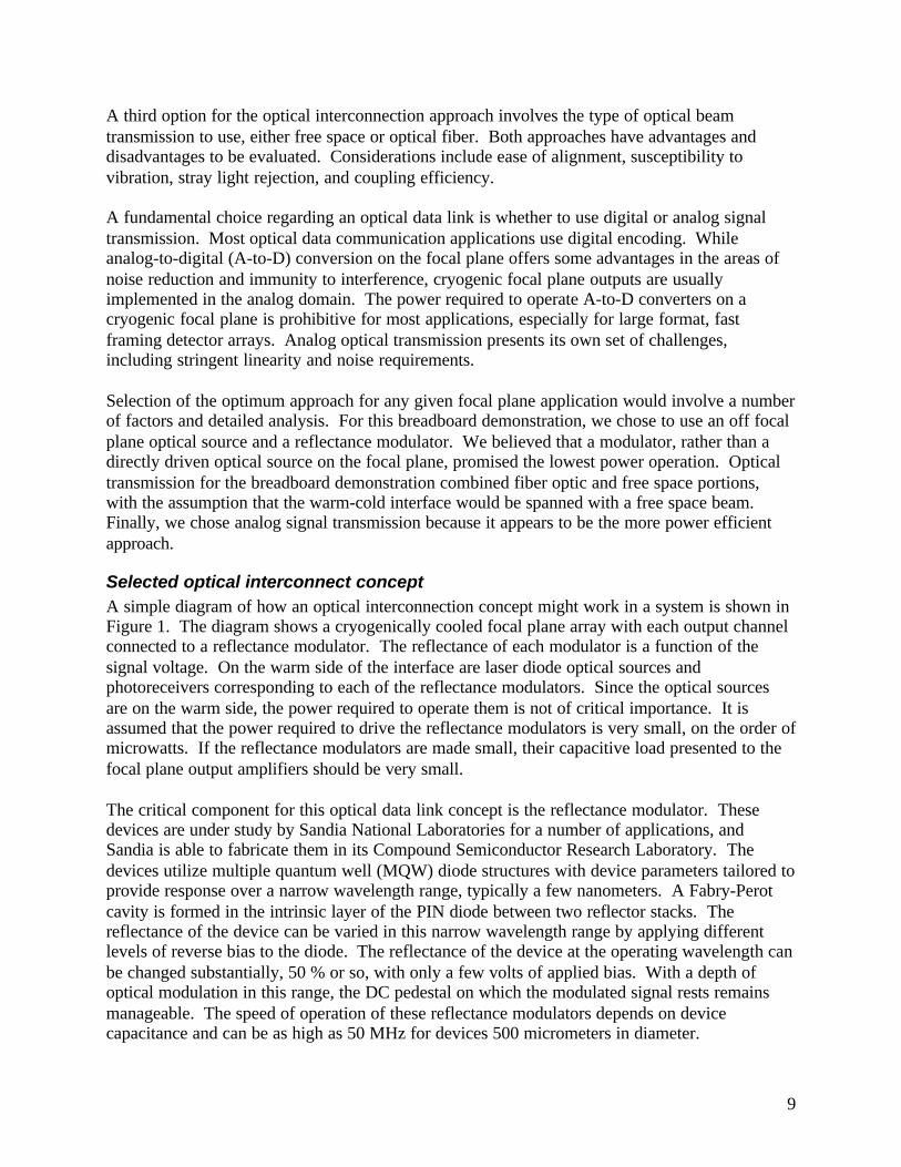
Retroreflector modulatorAs work began on this project we became aware of a related Sandia project to demonstrate freespace optical communications links. This project made use of a retroreflector modulator designwhich redirected a laser beam back on itself as the retroreflector modulated the optical intensity.Since the principal components were already set up in a laboratory, we decided to make use ofthe apparatus for a preliminary concept demonstration. The only significant modifications wemade to the setup were the use of a focal plane array output signal to drive the retroreflectormodulator and a photodetector module with increased gain to boost the voltage signal at the endof the optical link.
A diagram of the preliminary concept demonstration based on the retroreflector modulator isshown in Figure 2. The focal plane array used for this demonstration was the Detector ArrayReadout Test (DART) chip, designed and built at Sandia under another project. This focal planearray is well suited to this demonstration for a number of reasons. It can be operated with verysimple control electronics, requiring only one clock signal and one 5 volt DC power supply toproduce the focal plane output signal. Its signal output range is approximately 1.3 - 3.5 volts,which allows direct connection to the modulator without any gain or level shifting.
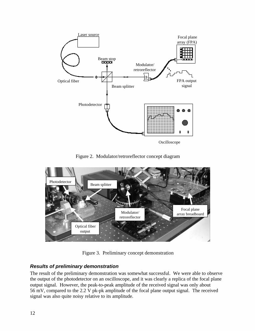
Figure 3 is a photograph of the preliminary concept demonstration. The laser operated in theshort wavelength infrared region of the spectrum. The photodetector is a Thorlabs modelPDA255 with a 1 mm diameter InGaAs photodiode and a built-in amplifier with atransimpedance gain of 104 volts/amp. The specified bandwidth of the photodetector is 50 MHz.We added a 1 inch diameter short focal length lens in front of the photodetector to help collectthe full beam width and focus it on the 1 mm diameter photodiode. The focal plane array wasoperated at an output rate of 105 pixels/second.
12
Laser source
Beam splitter
Beam stop
Optical fiber
Modulator/retroreflector
Focal planearray (FPA)
FPA outputsignal
Photodetector
Oscilloscope
Figure 2. Modulator/retroreflector concept diagram
Optical fiberoutput
Modulator/retroreflector
Focal planearray breadboard
PhotodetectorBeam splitter
Figure 3. Preliminary concept demonstration
Results of preliminary demonstrationThe result of the preliminary demonstration was somewhat successful. We were able to observethe output of the photodetector on an oscilloscope, and it was clearly a replica of the focal planeoutput signal. However, the peak-to-peak amplitude of the received signal was only about56 mV, compared to the 2.2 V pk-pk amplitude of the focal plane output signal. The receivedsignal was also quite noisy relative to its amplitude.

13
We investigated the weak signal by estimating the optical power received by the photodetectorand comparing it with the optical power measured at several positions in the optical path.Table 1 shows the power measured with a germanium radiometer probe (3 mm diameter) at threepositions in the optical path. By slightly varying the position of the radiometer probe, we werefairly certain the laser beam was underfilling the radiometer probe and the numbers shownrepresent the total optical power in the beam. The third row in Table 1 shows the input to thePDA255 detector with zero volts on the modulator. The loss at this point is fairly large, but isconsistent with a 3 dB loss through the beam splitter and the loss due to the small size of themodulator/retroreflector. The last line shows the signal power collected by the PDA255 detectorwith zero volts on the modulator. The output signal voltage was referenced back to receivedpower using the data sheet responsivity of 8,200 volts/watt at the operating wavelength. The lossat this point is probably due to reflection off the uncoated collecting lens and less than idealfocusing of the beam spot onto the small detector area. The measured losses at each point wereconsistent with our expectations. However, the laser power input to the beam splitter was muchlower than the 20 mW or so we had anticipated.
Table 1. Optical Power Measurements
Measured CouplingPower (mW) Factor Loss (dB)
Input to Beam Splitter 0.8390Input to Modulator 0.4400 0.5244 -2.8Input to Detector 0.0290 0.0659 -11.8Signal from Detector 0.0195 0.6728 -1.7
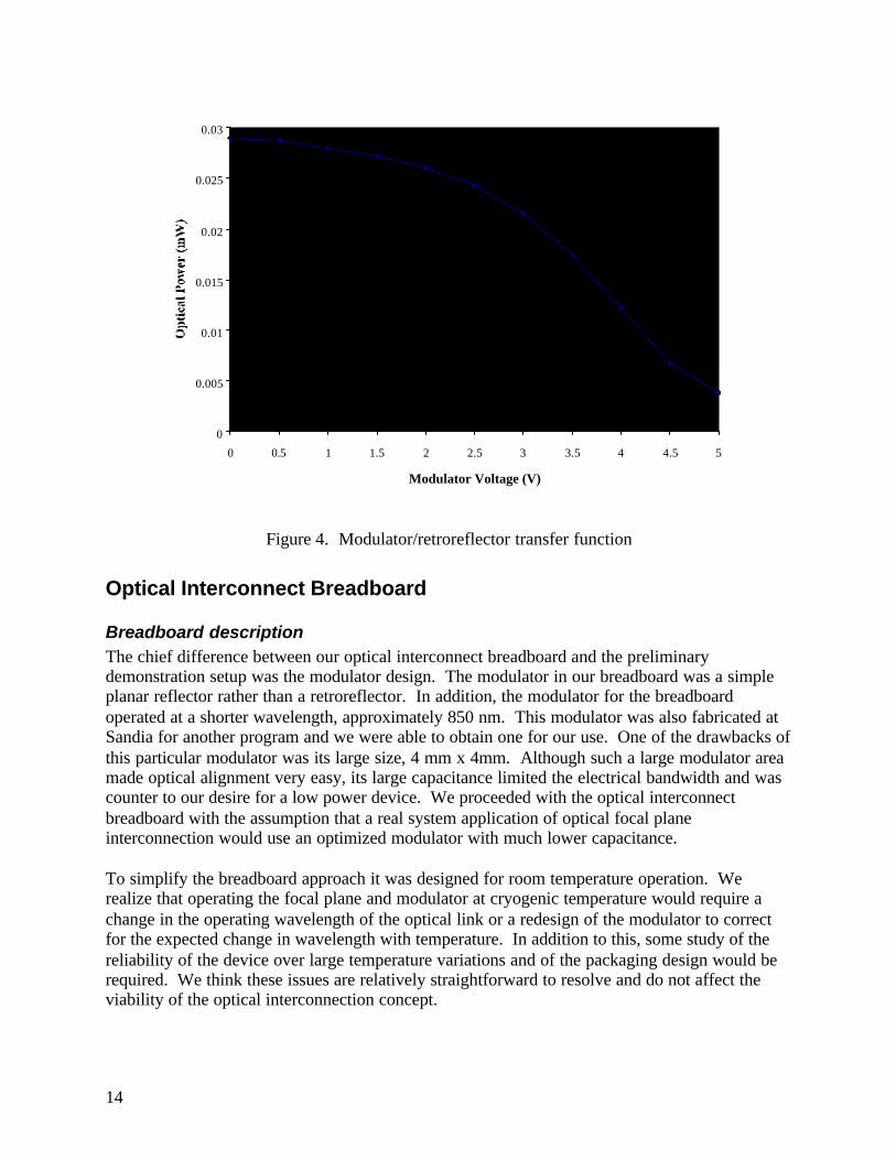
We also performed a quick measurement of the transfer curve of the optical power input to thedetector as a function of modulator voltage. The results are shown in Figure 4.
The output voltage range for the DART focal plane array is approximately 1.3 - 3.5 volts. Giventhe detector signal at zero modulator voltage from Table 1, the detector responsivity, and thetransfer function of Figure 4, the estimated peak-to-peak signal output using the DART array andthe modulator/retroreflector agreed very closely with the measured amplitude of 56 mV.
After making these measurements we were fairly confident we understood the optical throughputof the preliminary demonstration setup. We showed that the focal plane output signal could betransmitted over an optical link. With greater input laser power and a more efficient modulatordesign, a modulated signal amplitude approaching 1 volt should be possible.
14
0
0.005
0.01
0.015
0.02
0.025
0.03
0 0.5 1 1.5 2 2.5 3 3.5 4 4.5 5
Modulator Voltage (V)
Figure 4. Modulator/retroreflector transfer function
Optical Interconnect Breadboard
Breadboard descriptionThe chief difference between our optical interconnect breadboard and the preliminarydemonstration setup was the modulator design. The modulator in our breadboard was a simpleplanar reflector rather than a retroreflector. In addition, the modulator for the breadboardoperated at a shorter wavelength, approximately 850 nm. This modulator was also fabricated atSandia for another program and we were able to obtain one for our use. One of the drawbacks ofthis particular modulator was its large size, 4 mm x 4mm. Although such a large modulator areamade optical alignment very easy, its large capacitance limited the electrical bandwidth and wascounter to our desire for a low power device. We proceeded with the optical interconnectbreadboard with the assumption that a real system application of optical focal planeinterconnection would use an optimized modulator with much lower capacitance.
To simplify the breadboard approach it was designed for room temperature operation. Werealize that operating the focal plane and modulator at cryogenic temperature would require achange in the operating wavelength of the optical link or a redesign of the modulator to correctfor the expected change in wavelength with temperature. In addition to this, some study of thereliability of the device over large temperature variations and of the packaging design would berequired. We think these issues are relatively straightforward to resolve and do not affect theviability of the optical interconnection concept.

15
Other than the reflectance modulator, all the components for the optical interconnect breadboardare commercially available. A diagram of the optical interconnect breadboard is shown inFigure 5. Continuous wave optical illumination is provided by a SDL-5401 laser diode installedin a Newport model 700 temperature controlled mount with collimating optics option. ANewport model 505 laser diode driver and a model 350 temperature controller provide inputs tothe laser diode and maintain the desired temperature. The output from the laser diode is coupleinto an optical fiber for ease of positioning near the modulator. The optical fiber has a GRIN(GRaded INdex) rod at its output end to provide relatively low beam divergence. The beamreflected off the modulator is received by the same Thorlabs PDA255 photodetector moduledescribed earlier. The output signal from the photodetector is sent to a computer controlled dataacquisition system that is typically used for focal plane array output signals. This systemprovides for digitization, storage, and analysis of focal plane array data.
Optical fiber
Reflectancemodulator
Focal planearray (FPA)
FPA outputsignal
Photodetector
Data acquisitionsystem
Laser diodedriver
Temperaturecontroller
Figure 5. Optical interconnect breadboard concept
A photograph of the optical interconnect breadboard setup is shown in Figure 6 and a close-upphotograph of the fiber collimator, reflectance modulator, and photodetector is shown inFigure 7.
The following sections provide more details about the breadboard components and themeasurements made to characterize their performance.

16
Laser diodemount
Optical fiber
Focal planearray breadboard
Data acquisitionsystem input
Reflectancemodulator
Photodetector
Figure 6. Optical interconnect breadboard setup
Optical fiberoutput
Photodetector
Reflectancemodulator
Figure 7. Close-up of reflectance modulator
Reflectance modulatorThe MQW reflectance modulator is the key component of this particular approach to opticalinterconnection of focal plane array output. The modulator must exhibit a substantial variation

17
in its reflectance as the voltage on the device is changed, and the voltage required to alter thereflectance should be on the order of a few volts or less. For an actual optical interconnectapplication the device capacitance should be small to reduce the drive requirements on the focalplane output amplifier. As mentioned above, the reflectance modulator we were able to obtainfor this breadboard demonstration was larger than needed (4 mm x 4 mm) and had a much largercapacitance than desired. The minimum area required for the modulator depends on the opticalspot size on the device. A larger modulator would make alignment easier and would reduce theeffects of mechanical vibration.
The MQW reflectance modulator operates over a narrow wavelength range. We measured thereflectance versus wavelength at different modulator voltages using a monochromator todetermine the optimum laser wavelength. The results are shown in Figure 8.
0
0.1
0.2
0.3
0.4
0.5
0.6
0.7
0.8
0.9
830 835 840 845 850 855 860 865
Wavelength (nm)
0 V1 V2 V3 V
4 V5 V
Figure 8. Modulator reflectance versus wavelength
We can define a modulation factor, M, for two voltages, Vmin and Vmax. If r(V) is the reflectancefor a given modulator voltage, the modulation factor is
( ) ( )( )min
maxmin
VrVrVr
M−
=
A high modulation factor is desirable because it reduces the DC offset in the received signal andsimplifies the requirements for downstream gain and offset adjustments. The modulation factor

18
is plotted in Figure 9 for a 1 to 3 volt and a 2 to 4 volt signal range. From these plots, theoptimum wavelength appears to be 849 nm.
-0.1
0
0.1
0.2
0.3
0.4
0.5
0.6
830 835 840 845 850 855 860 865
Wavelength (nm)
1-3 Volt2-4 Volt
Figure 9. Modulation factor versus wavelength
Modulator reflectance versus voltage was measured at 849 nm and is shown in Figure 10.
We measured the reflectance modulator’s capacitance as a function of modulator voltage. Sincethe modulator is a reverse biased PIN diode, we expected the capacitance to decrease withincreasing operating voltage. The results of the capacitance vs. voltage measurements at100 kHz and 1 MHz are shown in Figure 11. For the output voltage range of a typical focalplane array, the modulator capacitance is roughly 3,000 pF. Assuming a modulator of 500 µmdiameter, a size more appropriate for focal plane optical interconnection, the capacitance wouldscale to 37 pF. Further refinements in modulator design could perhaps decrease the capacitanceper unit area.

19
0
0.05
0.1
0.15
0.2
0.25
0.3
0 0.5 1 1.5 2 2.5 3 3.5 4 4.5 5
Modulator Voltage (V)
Figure 10. Modulator reflectance versus voltage at 849 nm
0
1
2
3
4
5
6
0 0.5 1 1.5 2 2.5 3 3.5 4 4.5 5
Modulator Voltage (V)
100 kHz1 MHz
Figure 11. Reflectance modulator capacitance versus wavelength

20
While experimenting with the breadboard apparatus, we became aware that laser illumination onthe reflectance modulator produced a photocurrent. This is not surprising since the device is aPIN diode. We measured the spectral responsivity and quantum efficiency of the modulator at 2volts bias, and the results of the quantum efficiency measurements are shown in Figure 12. It isnotable that the quantum efficiency is above 30 percent at the operating wavelength, andsubstantial photocurrent is generated as the incident laser power is increased to produce a largersignal.
0
0.05
0.1
0.15
0.2
0.25
0.3
0.35
0.4
830 835 840 845 850 855 860 865
Wavelength (nm)
Figure 12. Modulator spectral quantum efficiency at 2 volts reverse bias
Laser diode sourceSecond only to the modulator performance characteristics, the noise of the laser source is acritical aspect of the selected optical interconnect concept. Lasers for optical communication canbe characterized by a relative intensity noise (RIN) parameter. Since the fields of optical andradio frequency data links deal mostly with noise and signal power ratios, the RIN parameter is anoise power to signal power ratio normalized by the noise bandwidth, ∆f. If plaser is the rootmean square laser intensity variation, and Plaser is the laser power, RIN is defined as
f1
PRIN 2
laser
2laser
∆⋅=
p
This normalized power ratio is usually expressed in dB/Hz.

21
Semiconductor diode lasers are known to be susceptible to intensity fluctuations, mode hopping,and other instabilities, especially when back reflections introduce unwanted feedback into thelasing cavity. Solid state lasers, such as Ti:Sapphire, can have lower RIN values than diodelasers, but their efficiency is lower as well. A good solid state laser may have a RIN value betterthan -160 dB/Hz. Since the objective of this project was to demonstrate a low power optical linkfor satellite applications, we chose to use a temperature controlled diode laser and find out howwell it could perform.
Given our experience with the preliminary demonstration apparatus and the lack of availableoptical power, we chose a laser diode with plenty of power. The SDL-5401 we selected has amaximum power output of 50 mW, which was more than enough to overcome any optical losseswe anticipated for the breadboard setup. The specified output wavelength is 852 nm ± 4 nm witha temperature coefficient of wavelength of 0.3 nm/°C. After receiving the laser diode wemeasured the output wavelength as a function of temperature using an Alton Instruments LM-30wavelength meter. The results are shown in Figure 13. The measurement was limited by theresolution of the wavelength meter, but it was clear that the desired operating temperature for849 nm output is around 26-27 °C. The measured temperature coefficient of wavelength is closeto 0.2 nm/°C, somewhat lower than specified.
y = 0.1947x + 843.56
846
846.5
847
847.5
848
848.5
849
849.5
850
850.5
10 15 20 25 30 35
Temperature (deg C)
Figure 13. Laser diode output wavelength versus temperature
We observed some of the undesirable characteristics of diode lasers with the breadboard setup.We found that active temperature control of the laser diode helped to reduce mode hopping andoverall laser intensity noise. Choice of the precise operating temperature was achieved through abalance of output wavelength and observed laser stability. Laser noise was found to vary

22
considerably over periods of several minutes, but we were able to make measurements lasting afew seconds during the relatively quiet intervals.
We made several measurements of laser noise at various places in the breadboard optical pathusing the PDA255 photodetector. The results of our laser noise measurements are shown inTable 2. We define a laser relative noise (LRN) parameter, which is simply the ratio of the RMSvoltage noise of the photodetector with the laser on, slaser , relative to the laser signal, Slaser. LRNis related to RIN by the following equation.
fRINLRN ∆⋅=
Table 2. Laser Noise Measurements
Measured at output of: Slaser (mV) slaser (mV) LRN RIN (dB/Hz)Laser diode 1473 0.923 6.266E-04 -136.6Fiber collimator 2292 1.748 7.626E-04 -134.9Modulator (open circuit) 1516 1.523 1.005E-03 -132.5
The increase in laser relative noise at points further along the optical path may indicate theeffects of optical feedback and mechanical vibration. There are some well known techniques toimprove RIN, such as antireflection coatings, optical isolators, and angle polished fiberconnectors. We could also have the laser diode coupled to an angle polished fiber pigtail.
Fiber opticsThe temperature controlled laser diode mount included an optical collimator with mediumprecision x, y, and z adjustment capability. The collimated beam was transmitted over a shortdistance (less than 1 cm) to a collimating optic assembly (Thorlabs F220FC-B) installed in a tip-tilt mount. Multimode optical fiber with 65.5 µm core diameter was used to deliver the beam tothe reflectance modulator. Rather than varying the laser diode current to change the deliveredoptical power, we purposely defocused and misaligned the fiber optic input.
The output end of the optical fiber included a GRIN rod output collimator to reduce beamdivergence. The output collimator was positioned about 1 cm from the optical modulator andtilted with respect to it to provide an angle of incidence roughly 10 degrees from normal.
PhotodetectorThe Thorlabs PDA255 high speed photodetector was briefly described in the description of thepreliminary concept demonstration. The 1 mm diameter InGaAs photodiode coupled with atransimpedance amplifier using a 10 kΩ feedback resistor has a data sheet responsivity at850 nm of about 2,000 volts/watt. We did not use a collecting optic in front of the detectorbecause the beam divergence was low and the beam path was short. Higher responsivity couldhave been achieved if we had procured a similar photodetector using a silicon photodiode.
The electronic bandwidth of the photodetector module is 50 MHz, but we used a simple RC lowpass filter at the input to the data acquisition system. We typically use such a filter when testing

23
focal plane arrays to limit the noise bandwidth while allowing enough signal bandwidth to permitadequate settling between pixel values. For these tests the noise bandwidth was limited to17.9 MHz.
The maximum RMS noise given in the data sheet of the PDA255 photodetector is 2.0 mV. Wethink it’s possible to do better than this with a custom designed photodiode and amplifier. Withthe reduced noise bandwidth provided by the low pass filter, the calculated maximum noise isapproximately 0.95 mV.
Measured Breadboard PerformanceWith all the components of the breadboard system set up and aligned, we proceeded with thedemonstration of optical interconnect performance. We allowed the laser diode to stabilize whileoperating at 25.9 °C. Operation of the DART focal plane array was started and its output wasconnected to the reflectance modulator. We observed the output from the optical interconnectlink on an oscilloscope and compared it with the input direct from the focal plane array. Anoscilloscope photo with both output and input is shown in Figure 14. The upper trace shows theoptical interconnect output on a 500 mV per division scale. The lower trace is the inverted inputfrom the focal plane at 1 V per division.
Figure 14. Optical interconnect output and DART focal plane output
The traces show approximately 1 frame of data for the 128 row x 16 column test array. TheDART test array is composed of 8 subarrays of 16 x 16 pixels each, which represent various unitcell design approaches. This creates regions of the output waveform at substantially differentvoltage levels. The isolated spikes in the output waveform are due to individual bad pixelswhich deviate from the normal output level for a given subarray. These bad pixels are actuallyquite useful for assessing the adequacy of the electronic bandwidth of the output amplifier anddata acquisition system.

24
The voltage modulation at the output of the optical link is smaller than the input voltagemodulation. It was assumed we could simply increase the laser power to achieve a larger outputvoltage swing. We found, however, that there was a limit to the optical power illuminating themodulator while maintaining link operation. When the optical power was increased to producean output voltage swing greater than about 0.6 volts, the input signal from the DART array andthe optical interconnect output signal became very unstable and both collapsed at higher inputsignal levels.
We think this optical power limit is due to photocurrent generated in the reflectance modulator.Recalling that the absorption quantum efficiency of the modulator is over 30 percent in thiswavelength region, approximately 200 µA of photocurrent is produced for each milliwatt of laserpower incident on the modulator. Given the polarity of the modulator PIN junction, thisphotocurrent must be supplied by the output amplifier of the focal plane array in order tomaintain the input signal voltage. If this photocurrent cannot be supplied by the focal planeoutput amplifier, the voltage on the input sags to a lower level. For photocurrent above a certainlevel the focal plane array output amplifier is not able to generate any significant input signal tothe optical link.
Photocurrent generated in the reflectance modulator also limits the maximum pixel rate. Thetraces in Figure 14 were obtained at a pixel rate of 100 kilopixels per second. Although wetypically operate the DART array at an output rate of 1 megapixel per second, both the inputfrom the DART array and the optical interconnect output were distorted at the higher pixel rate,as shown in Figure 15.
Figure 15. Output traces at 1 megapixel/second

25
To gain insight into what may be happening, Figure 16 shows 1 megapixel per second input andoutput traces at an expanded time base. The waveforms of the bad pixels are clearly skewed andseem to be limited by the slew rate in one direction rather than an RC time constant. The lowertrace representing the input from the DART focal plane has been inverted relative to the actualfocal plane output, so the slew rate limit appears as the focal plane signal attempts to changefrom a lower to a higher voltage. This is what one would expect if the output amplifier is tryingto supply the modulator photocurrent as well as driving to a higher voltage. For the higher tolower signal transition, the photocurrent actually aids the transition speed and the slew rate isvery fast.
Figure 16. Expanded 1 megapixel/second output trace
To characterize the overall performance of the optical interconnect breadboard, we made a seriesof signal and noise measurements at different laser power levels. We made use of our focalplane array data acquisition system to digitize and store the data and to calculate RMS noise andsignal amplitude. The RMS noise was determined by calculating the temporal standard deviationfor each pixel over 128 frames and then finding the median value for all the pixels in thesubarray. Because of the variety of subarrays on the DART focal plane array and differentpolarities of unit cell designs, certain subarrays are at the minimum voltage level and othersubarrays are at the maximum level. Therefore, each frame of input signal from the array spansthe available input voltage range. The total signal swing at both the input and output can bedetermined from the oscilloscope waveforms without changing the light level incident on thefocal plane. All the following measurements were made with the focal plane in the dark.
We measured the DART focal plane output voltage swing, ∆V, and noise voltage, v, undervarious conditions and calculated the signal to noise ratio. The results are shown in Table 3.Loading of the focal plane output amplifier by the laser induced modulator photocurrent isevident. Laser power on the modulator also increases the focal plane output noise level,

26
probably through coupling of laser intensity noise to the output voltage level through variationsin the photocurrent. With the laser off, the modulator provides a bit of noise filtering because ofits large capacitance. This may explain the slightly higher noise when the modulator isdisconnected.
Table 3. DART FPA Signal and Noise Levels
∆V (mV) v (mV) ∆V/vModulator connected, laser on 2100 1.23 1710Modulator connected, laser off 2266 0.97 2333Modulator disconnected 2266 0.99 2286
We then measured the signal swing, ∆S, and noise voltage, snoise, for the optical interconnectoutput at 4 different laser power levels and calculated the signal to noise ratio. To quantify thenoise added by the optical interconnect link, we compare the voltage SNR at the focal planeoutput when the modulator was disconnected to the voltage SNR at the optical interconnectoutput. SNR is degraded through the optical link by a factor of 10 or more. This ratio expressedin dB is the link noise figure, LNF. These results are shown in Table 4.
Table 4. Optical Interconnect Signal and Noise Levels
∆S (mV) snoise (mV) ∆S/snoise SNRin/SNRout LNFTrial 1 170.9 1.24 137.6 16.61 24.4Trial 2 258.8 1.45 179.1 12.77 22.1Trial 3 449.2 1.91 235.1 9.73 19.8Trial 4 600.6 2.57 233.9 9.78 19.8
Analysis of Measurements
Calculated signal swingWe can analyze the throughput of the optical interconnect breadboard, and determine if themeasured output signal levels are reasonable. Let α represent the coupling efficiency of the lightreflected by the modulator and received by the photodetector. Letting R represent the voltageresponsivity (volts/watt) of the photodetector and recalling that r(V) is the modulator reflectanceas a function of voltage, the output signal swing when the input changes from Vmin to Vmax is
( ) ( )[ ]maxminlaser VrVrPS −⋅⋅⋅α=∆ R
After the four measurement trials the optical power was adjusted to provide an output signalswing of roughly 500 mV. The laser power at the output collimator just ahead of the reflectancemodulator was measured to be 2.39 mW. With the DART focal plane array connected to themodulator and the laser running, Vmin and Vmax were measured to be 1.18 V and 3.28 V,

27
respectively. Using reflectance values interpolated from Figure 10 and a voltage responsivity of2,000 volts/watt, the coupling efficiency was calculated to be greater than 90%.
The laser power incident on the modulator for most of these measurements was much lower thanthe maximum power available from the laser diode. We attenuated the optical power at themodulator by purposely misaligning the optical input coupling to the fiber. To evaluate theminimum optical loss, we tweaked the input coupling and measured the power into and out ofthe optical fiber. At a laser diode temperature of 25.9 °C and a drive current of 50 mA, themeasured optical power out of the laser diode collimating optic was 38.6 mW. The measuredpower out of the fiber just ahead of the modulator was 22.55 mW, for a coupling efficiency of0.584 (-2.3 dB). A much lower power laser diode would be used in an actual opticalinterconnect application.
Calculated noiseThe components of the total output noise we consider are FPA noise at the input to the opticalinterconnect, photodetector dark noise due to its amplifier, photodetector shot noise, and laserintensity noise. To compare the calculations with measured data, we express the noise as afunction of output signal swing, ∆S. All these noise sources depend on ∆S except forphotodetector amplifier noise. For this analysis, data acquisition system noise is included withphotodetector noise. The noise of the photodetector under dark conditions, sdet, was measured tobe 1.11 mV.
Photodetector shot noise, sshot, increases as the square root of the photocurrent generated in thesensing element, and is given by the equation
( ) fVrRPq2fIq2R fblaserphotofbshot ∆⋅⋅⋅⋅⋅α⋅⋅=∆⋅⋅⋅= Rs
Rfb is the feedback resistor value of the photodetector transimpedance amplifier. Using therelationship between laser power and output signal swing, and definingβ(V) = r(V)/[r(Vmin) - r(Vmax)], we have
( ) SfVRq2 fbshot ∆⋅∆⋅β⋅⋅⋅=s
For the reflectance modulator used and the DART array output voltage range, β(V) variesbetween 0.879 at Vmax to 1.879 at Vmin. The noise measurements corresponded to a portion ofthe output signal which was at Vmax, so the minimum value of β was used in the noisecalculation.
Noise voltage present at the FPA output is amplified or attenuated by the link gain, which isdefined as the ratio of ∆S to ∆V. FPA noise, sfpa is simply
SVfpa ∆⋅
∆=
vs
The output noise due to laser intensity noise is given by

28
( ) Rs ⋅⋅⋅⋅α= VrPLRN laserlaser
Expressing this in terms of ∆S, we have
( ) SLRNVlaser ∆⋅⋅β=s
Laser relative noise measured at the output of the modulator was used for the noise calculation.As given in Table 2, the LRN at this location in the optical interconnect is 1.005E-03.
Total noise variance for the optical interconnect output is, therefore
( )( ) ( )( ) 222
fb2
det2
total SLRNVV
SfVRq2 ∆⋅
⋅β+
∆+∆⋅∆⋅β⋅⋅⋅+=
vss
(Total noise equation)
We can compare the total output noise predicted by this expression with the measured noise atthe four different ∆S values achieved by varying the laser power. Predicted noise and measurednoise are shown in Figure 17.
0.E+00
1.E-06
2.E-06
3.E-06
4.E-06
5.E-06
6.E-06
7.E-06
8.E-06
0 0.05 0.1 0.15 0.2 0.25 0.3 0.35 0.4
Signal Swing Squared (V2)
MeasuredPredicted
Fit
Figure 17. Noise squared versus signal swing squared

29
The measured data points show a linear relationship between noise and signal as predicted by thetotal noise equation, but the predicted slope is much less than that determined by the measureddata. Using the slope of the trend line applied to the measured data, the value of LRN implied bythe output noise data is 4.377E-03, a factor of 4.36 greater than the measured LRN. The linelabeled “Fit” in Figure 17 represents the noise recalculated to fit the effective LRN determinedby the output noise data.
The cause for this discrepancy has not been determined, but we observed that laser noise variedconsiderably during our measurements. There is also the possibility of photocurrent generated inthe modulator affecting the noise output of the FPA and leading to an increase in the effectiveLRN.
Using an effective LRN term which tracks the measured data, we can examine the noise sourcesto determine the dominant ones. Figure 18 shows the components of the total squared noise forthe four values of ∆S. Detector noise and laser noise are the dominant contributors to outputnoise.
0.E+00
1.E-06
2.E-06
3.E-06
4.E-06
5.E-06
6.E-06
7.E-06
0.171 0.259 0.449 0.601
Signal Swing (V)
LaserFPAShot
Detector
Figure 18. Components of squared noise
From the total noise equation, we see that the ratio of noise to signal swing, stotal/∆S approaches aconstant value at large values of ∆S and is dominated by LRN.

30
Potential performance improvementExamination of the equation for total noise allows us to determine the potential performanceimprovements that can be made. One of the goals for design of an optical interconnect system isto minimize the degradation in SNR from link input to link output. The first priority is reductionin laser relative noise. Inspection of the total noise equation indicates that LRN should satisfythe following inequality
( )VVLRN
β⋅∆<<
v
For the DART array signal and noise values and the β value of the reflectance modulator, LRNshould be much less than 4.975E-04. This corresponds to a value for RIN of -138.6 dB/Hz. TheLRN measured directly from our laser diode approached this level, but the apparent increase inLRN evident in the output noise was substantially higher.
Assuming LRN is reduced sufficiently, the shot noise term determines the value of ∆S needed tokeep it from limiting SNR. The following inequality determines the minimum signal swingrequired.
( )( )2
fbV
fVRq2S
∆
⋅∆⋅β⋅⋅⋅>>∆v
For the values applicable to our breadboard system, ∆S should be much greater than 264 mV.
To achieve optimum performance, the detector noise also needs to be reduced. For a situationwhere the shot noise and laser noise contributions are small, the detector noise should meet thefollowing requirement
VS
det ∆∆
⋅<< vs
As with the shot noise term, the detector noise term calls for a larger value of ∆S to optimizeperformance. Any parameter that increases link gain will reduce the effect of detector noise.The photodetector used for the breadboard setup was not optimized for the wavelength used. Afactor of 3 improvement in ∆S could be easily achieved using a silicon photodetector. Highertransimpedance gain may also help the situation. However, the required electronic bandwidthmay be difficult to achieve with a single amplifier stage. Multiple amplifier stages could be usedto boost ∆S while maintaining bandwidth.
Figure 19 illustrates the performance improvement that could be achieved if laser intensity noiseand detector noise are reduced below the other noise sources. The first curve shows SNR versussignal swing for the total noise calculated with the LRN figure derived from the output noisedata. This curve corresponds to the noise levels measured in our breadboard setup. The secondcurve shows the limit to SNR imposed by the high level of laser intensity noise. The third curveshows the SNR level that could be achieved if laser noise and detector noise are reduced to levels

31
where only shot noise and FPA noise remain. The fourth curve shows the limit to SNR governedby the FPA noise level at the input to the optical link.
0
500
1000
1500
2000
2500
0 0.5 1 1.5 2 2.5 3
Signal Swing (V)
TotalLaserFPA+Shot
FPA
Figure 19. Component SNR versus output signal swing
Suggestions for Further Work
Improved sourceFrom the above analysis it is clear that a low noise laser source is required. A RIN valueapproaching -160 dB/Hz is a goal. As stated earlier, the compactness and high efficiency ofsemiconductor diode lasers are attractive, but a substantial improvement in their intensity noiseneeds to be achieved. Solid state lasers should also be investigated to determine if theirefficiency can be made high enough to be used for an optical link without increasing total systempower. With careful selection of the laser source for lower intensity noise, the link noise figurecould be lowered substantially.
Improved modulatorThe primary motivation for this work is to decrease the power required by the FPA outputamplifiers. The capacitance per unit area for the modulator used in this project is fairly high. Itwould be desirable for modulator capacitance to be on the order of a few picofarads for a 500 µmdiameter device.
The photocurrent produced by the MQW modulator is troublesome and imposes a current loadon the FPA output amplifier. Even if higher overall reflectance could be achieved, the desire for

32
a large modulation factor would lead to higher absorption and greater photocurrent for part of theoutput signal range. It would be useful to investigate whether or not lower reflectancenecessarily comes at the expense of higher photocurrent. If the photocurrent can be reduced, itshould be possible to use greater laser power and obtain a larger output signal swing.
Lower noise detectorA careful analysis of design requirements and a custom approach to the photodetector couldsubstantially improve performance. A photodiode with spectral response matched to theoperating wavelength coupled with a low noise amplifier should easily improve on theperformance of the off-the-shelf item that was used.
Design tradeoffsSome of the other candidate concepts for focal plane optical interconnections could beinvestigated in future efforts. Given the issue of photocurrent generation in the reflectancemodulator, on-focal-plane optical sources begin to look more attractive. If a substantial portionof the incident optical beam is converted to photocurrent that needs to be supplied by the FPAoutput amplifier, the low power advantage of a reflectance modulator approach is not as great.Integration and alignment challenges may be reduced using direct modulation of optical sourceson the focal plane.
The system could potentially benefit from an investigation of free space versus fiber opticconnections for use with cryogenic focal plane arrays. The reliability and thermal conductanceissues with fibers spanning the warm to cold interface need to be studied. Free space opticalcoupling presents challenges in the areas of alignment and vibration control, especially when thedrive for low capacitance leads to small device area.
The use of a digital optical link is also a possibility for future study. However, this approachdepends on the implementation of A-to-D conversion on the focal plane. While on focal planeA-to-D conversion is becoming available for FPAs operating at room temperature, the powerdissipation penalty works against this approach for cryogenic focal plane arrays.
Future efforts could look more systematically at the full trade space and identify thoseapproaches holding the most promise. Performance requirements for individual componentscould be specified, and demonstrations of key device characteristics could be planned.
Summary and ConclusionsThe objective of this project was to identify several concepts for focal plane opticalinterconnection and to demonstrate one of those concepts using an actual focal plane arrayoutput. With both a preliminary demonstration setup and an optical interconnect breadboard wesuccessfully demonstrated transmission of focal plane array output waveforms over optical links.The remainder of the project focused on characterizing the performance of the opticalinterconnect breadboard and analyzing the results to understand the key performance drivers.
The optical interconnect approach we selected and demonstrated made use of a reflectancemodulator fabricated with multiple quantum well technology. A CW laser source was aimed atthe modulator, and the analog focal plane output signal was impressed on the reflected beam due

33
to the modulator’s voltage dependent reflectance. The laser source was a temperature controlleddiode laser operating at 849 nm. The received signal was fed into the same data acquisition andanalysis system we use for focal plane array characterization.
We performed a number of measurements to assess the characteristics of the optical link outputsignal relative to the input signal from the focal plane array. The signal to noise ratio wasdegraded a factor of 10 or more by the optical link, and the maximum output signal level waslimited due to photocurrent generation in the reflectance modulator and the limited current drivecapability of the focal plane output amplifier.
We analyzed the noise components of the optical interconnect breadboard and identified laserintensity noise and photodetector noise as the limiting sources. The noise in the measured outputsignal that behaved as laser intensity noise was higher than the direct laser noise measurementswould indicate. This discrepancy should be investigated further. Our analysis of noise sourcesestablished performance goals for laser sources and photodetectors for future efforts.
This project highlighted the design challenges involved with optical data links. By observing theperformance of actual devices and analyzing their behavior, we are better able to refine thisoptical interconnection approach and to investigate alternative approaches.

34
DISTRIBUTION:
1 MS 0603 D. K. Serkland, 17421 0603 C. T. Sullivan, 17431 0874 M. Armendariz, 17511 0874 G. R. Schuster, 17511 0860 C. L. Smithpeter, 26181 0965 K. R. Lanes, 57111 0972 A. J. Medina, 57201 0972 S. M. Gentry, 57224 0972 M. K. Hinckley, 57221 0972 R. R. Kay, 57226 0972 J. L. Rienstra, 57221 0188 LDRD Program Office, 10301 9018 Central Technical Files, 8945-12 0899 Technical Library, 96161 0612 Review & Approval Desk, 9612
For DOE/OSTI