Embed Size (px)
Citation preview
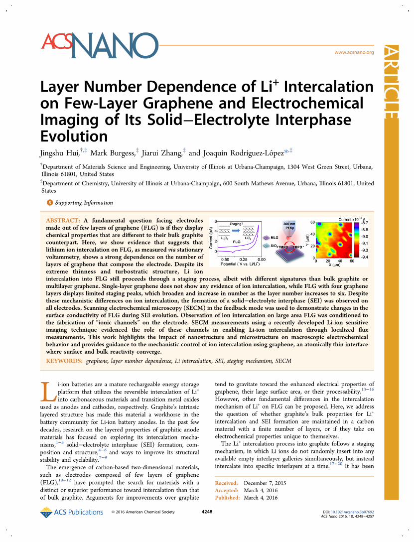
Layer Number Dependence of Li+ Intercalationon Few-Layer Graphene and ElectrochemicalImaging of Its Solid−Electrolyte InterphaseEvolutionJingshu Hui,†,‡ Mark Burgess,‡ Jiarui Zhang,‡ and Joaquín Rodríguez-Lopez*,‡
†Department of Materials Science and Engineering, University of Illinois at Urbana-Champaign, 1304 West Green Street, Urbana,Illinois 61801, United States‡Department of Chemistry, University of Illinois at Urbana-Champaign, 600 South Mathews Avenue, Urbana, Illinois 61801, UnitedStates
*S Supporting Information
ABSTRACT: A fundamental question facing electrodesmade out of few layers of graphene (FLG) is if they displaychemical properties that are different to their bulk graphitecounterpart. Here, we show evidence that suggests thatlithium ion intercalation on FLG, as measured via stationaryvoltammetry, shows a strong dependence on the number oflayers of graphene that compose the electrode. Despite itsextreme thinness and turbostratic structure, Li ionintercalation into FLG still proceeds through a staging process, albeit with different signatures than bulk graphite ormultilayer graphene. Single-layer graphene does not show any evidence of ion intercalation, while FLG with four graphenelayers displays limited staging peaks, which broaden and increase in number as the layer number increases to six. Despitethese mechanistic differences on ion intercalation, the formation of a solid−electrolyte interphase (SEI) was observed onall electrodes. Scanning electrochemical microscopy (SECM) in the feedback mode was used to demonstrate changes in thesurface conductivity of FLG during SEI evolution. Observation of ion intercalation on large area FLG was conditioned tothe fabrication of “ionic channels” on the electrode. SECM measurements using a recently developed Li-ion sensitiveimaging technique evidenced the role of these channels in enabling Li-ion intercalation through localized fluxmeasurements. This work highlights the impact of nanostructure and microstructure on macroscopic electrochemicalbehavior and provides guidance to the mechanistic control of ion intercalation using graphene, an atomically thin interfacewhere surface and bulk reactivity converge.
KEYWORDS: graphene, layer number dependence, Li intercalation, SEI, staging mechanism, SECM
Li-ion batteries are a mature rechargeable energy storageplatform that utilizes the reversible intercalation of Li+
into carbonaceous materials and transition metal oxidesused as anodes and cathodes, respectively. Graphite’s intrinsiclayered structure has made this material a workhorse in thebattery community for Li-ion battery anodes. In the past fewdecades, research on the layered properties of graphitic anodematerials has focused on exploring its intercalation mecha-nisms,1−3 solid−electrolyte interphase (SEI) formation, com-position and structure,4−6 and ways to improve its structuralstability and cyclability.7−9
The emergence of carbon-based two-dimensional materials,such as electrodes composed of few layers of graphene(FLG),10−12 have prompted the search for materials with adistinct or superior performance toward intercalation than thatof bulk graphite. Arguments for improvements over graphite
tend to gravitate toward the enhanced electrical properties ofgraphene, their large surface area, or their processability.13−16
However, other fundamental differences in the intercalationmechanism of Li+ on FLG can be proposed. Here, we addressthe question of whether graphite’s bulk properties for Li+
intercalation and SEI formation are maintained in a carbonmaterial with a finite number of layers, or if they take onelectrochemical properties unique to themselves.The Li+ intercalation process into graphite follows a staging
mechanism, in which Li ions do not randomly insert into anyavailable empty interlayer galleries simultaneously, but insteadintercalate into specific interlayers at a time.17−20 It has been
Received: December 7, 2015Accepted: March 4, 2016Published: March 4, 2016
Artic
lewww.acsnano.org
© 2016 American Chemical Society 4248 DOI: 10.1021/acsnano.5b07692ACS Nano 2016, 10, 4248−4257
reported that Li ions first randomly occupy available sites(dilute stage-1, LiC72), then diffuse to fill every four layers ofthe graphene planes (stage-4, LiC36), and finally concentrate tofill every three (stage-3, LiC27), two (stage-2, LiC12), and one(stage-1, LiC6) layer(s), respectively.8,21 Thus, in graphite theintercalation process is strongly dependent on the number ofneighboring delithiated interlayers at any given time. FLGnaturally displays limited numbers of available intercalationsites; therefore, we hypothesize that the staging of lithiation willbe necessarily limited as certain charge stages are not accessible.For example, stage-4 may not be possible in FLG with less than5 layer graphene. With limited interlayers for Li+ intercalationin FLG, this process might reveal different phase transitionsbetween stages and a deviation from intercalation potentialswhen compared to bulk graphite.Apart from Li+ intercalation, a SEI is also generated at the
early stages of cycling on graphite anodes. The SEI formsbecause the negatively polarized anode causes the degradationof electrolyte and solvent, causing deposition of inorganic andorganic decomposition products, onto the surface of thegraphite. However, after formation and stabilization, the SEIlayer prevents further degradation of electrolyte and solvent asthis layer is largely electronically insulating, thus blockingelectron transport across it.4−6 Yet even with the SEIcompletely formed, the anode maintains high Li+ conductivitywhich ensures long-term cyclability. Compared to graphite,FLG has similar surface properties and electrochemical
characteristics;22 thus, it may exhibit similar SEI formationprocesses. However, the stability of the SEI on FLG, togetherwith its electronic and ionic conductivity properties, has notbeen fully addressed.In this paper, we explored Li+ intercalation and SEI
formation on FLG via stationary voltammetry and electro-chemical imaging methods. Two synthetic routes were used tofabricate FLG. One consisted of the direct growth of multilayergraphene (MLG), which had on average 10 graphene layers.The other methodology consisted of the layer-by-layer transferof bilayer graphene (BLG), to controllably produce layerednumber graphene samples (2−6 layers). FLG samples revealeda layer number dependence for the number and location ofintercalation peaks, which is representative of the existence of astaging-type mechanism.Previous studies of the SEI on graphite were focused on the
structural, compositional and stability changes with differentcarbon materials, solvents, electrolytes, and temperatures usingspectroscopic and microscopic methods such as X-ray photo-electron spectroscopy,23,24 Fourier transform infrared spectros-copy,25 mass spectrometry,24 X-ray diffraction,26 and electronmicroscopy.24 Electrochemical impedance spectroscopy (EIS)is the most common method to explore SEI’s conductivity afterformation, but the information from these experiments isspatially averaged.27 Here, we introduce scanning electro-chemical microscopy (SECM) to visualize in situ the localelectronic transfer and ionic transport properties of FLG
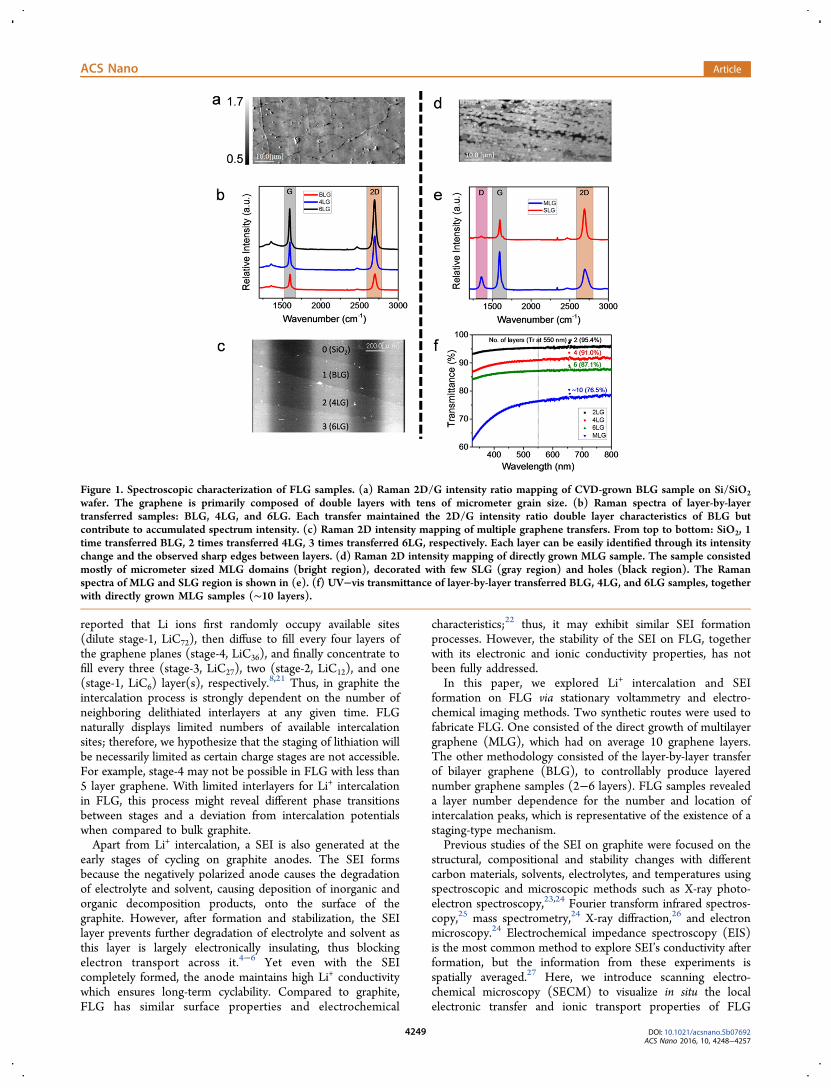
Figure 1. Spectroscopic characterization of FLG samples. (a) Raman 2D/G intensity ratio mapping of CVD-grown BLG sample on Si/SiO2wafer. The graphene is primarily composed of double layers with tens of micrometer grain size. (b) Raman spectra of layer-by-layertransferred samples: BLG, 4LG, and 6LG. Each transfer maintained the 2D/G intensity ratio double layer characteristics of BLG butcontribute to accumulated spectrum intensity. (c) Raman 2D intensity mapping of multiple graphene transfers. From top to bottom: SiO2, 1time transferred BLG, 2 times transferred 4LG, 3 times transferred 6LG, respectively. Each layer can be easily identified through its intensitychange and the observed sharp edges between layers. (d) Raman 2D intensity mapping of directly grown MLG sample. The sample consistedmostly of micrometer sized MLG domains (bright region), decorated with few SLG (gray region) and holes (black region). The Ramanspectra of MLG and SLG region is shown in (e). (f) UV−vis transmittance of layer-by-layer transferred BLG, 4LG, and 6LG samples, togetherwith directly grown MLG samples (∼10 layers).
ACS Nano Article
DOI: 10.1021/acsnano.5b07692ACS Nano 2016, 10, 4248−4257
4249
electrodes after SEI formation. SECM is a powerful tool toimage highly localized substrate electrochemical processes, andprovides a convenient platform to test comparisons betweenmaterials and substrate conditions within the same experiment.In our experiment, a Pt nanoelectrode was used to sense andimage local electrochemical kinetic changes before and after SEIformation through SECM feedback experiments. Additionally, aHg-capped Pt ultra-micro electrode was used as a spatiallyresolved selective Li-ion sensor via stripping voltammetry28 toexplore Li+ uptake into FLG with a formed SEI layer. Spatiallyresolved information about electron transfer kinetics and ionictransport of SEI coated MLG samples provided details of SEIlayer behavior changes in situ, and guided us to betterunderstand the SEI properties on ultrathin FLG samples.
RESULTS AND DISCUSSIONTo explore Li+ intercalation into FLG with different number oflayers, two different types of graphene substrates were grownusing chemical vapor deposition (CVD). One CVD methodreliably produced double layer graphene, which, after layer-by-layer transfer, yielded graphene with 2, 4, or 6 layers as needed.The other CVD method directly grew multilayer graphene.Figure 1 summarizes the properties of different graphenesamples. The Raman 2D/G ratio mapping in Figure 1a reflectsthe double layer structure of graphene, which displays a 2D/Gintensity ratio around 1.29,30 Graphene samples showed auniform and continuous sheet with tens of micrometer domainsize. After layer-by-layer transfer of bilayer graphene sheets, 2-,4-, and 6-layer graphene substrates were obtained. Figure 1c isthe Raman 2D intensity mapping of a three times transferredgraphene sample where each layer can be recognized with sharpedges, indicating the integrity of these samples was maintainedafter a layer-by-layer wet transfer. A zoomed-in view of eachlayer, the Raman spectra of 1, 2, and 3 times transfer graphenesamples are shown in Figure 1b. From these spectra, it is clearthat each layer preserved a 2D/G intensity ratio of about 1, anddouble and triple transferred samples exhibited 2 or 3 timeshigher intensities.31 With this method, we can successfullymanufacture bilayer graphene (BLG), 4-layer graphene (4LG),and 6-layer graphene (6LG) samples verified by Ramananalysis. Figure 1d shows the Raman 2D intensity mappingof directly grown multilayer graphene (MLG), where Ramanspectra of representative areas in MLG are shown in Figure 1e.In this figure, the white areas are multilayer graphene domains,gray areas are single-layer domains, and black areas are holes.Additional methods were used to characterize graphenesamples for verification. The gradual decrease of UV−vistransmittance (Figure 1f) for the progression from single,double, and triple layer-by-layer transferred bilayer graphene onglass agrees well with Raman images. According to previousreports, each layer of graphene contributes to a 2.3%transmittance decrease at 550 nm,32 as quantitatively observedfor our 2-, 4-, and 6-layer graphene sheets. From thetransmittance data of MLG (∼76%), this material was roughlyequivalent to 10 layers of graphene.After successfully making the graphene samples (2-, 4-, 6-
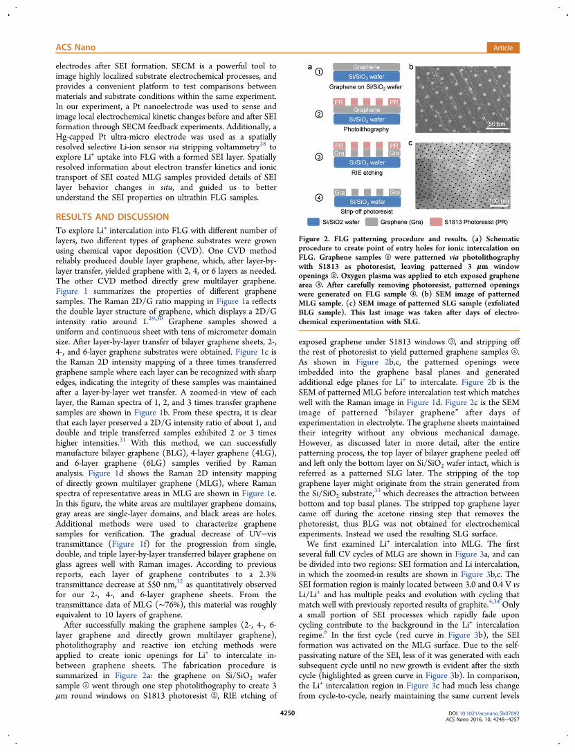
layer graphene and directly grown multilayer graphene),photolithography and reactive ion etching methods wereapplied to create ionic openings for Li+ to intercalate in-between graphene sheets. The fabrication procedure issummarized in Figure 2a: the graphene on Si/SiO2 wafersample ① went through one step photolithography to create 3μm round windows on S1813 photoresist ②, RIE etching of
exposed graphene under S1813 windows ③, and stripping offthe rest of photoresist to yield patterned graphene samples ④.As shown in Figure 2b,c, the patterned openings wereimbedded into the graphene basal planes and generatedadditional edge planes for Li+ to intercalate. Figure 2b is theSEM of patterned MLG before intercalation test which matcheswell with the Raman image in Figure 1d. Figure 2c is the SEMimage of patterned “bilayer graphene” after days ofexperimentation in electrolyte. The graphene sheets maintainedtheir integrity without any obvious mechanical damage.However, as discussed later in more detail, after the entirepatterning process, the top layer of bilayer graphene peeled offand left only the bottom layer on Si/SiO2 wafer intact, which isreferred as a patterned SLG later. The stripping of the topgraphene layer might originate from the strain generated fromthe Si/SiO2 substrate,
33 which decreases the attraction betweenbottom and top basal planes. The stripped top graphene layercame off during the acetone rinsing step that removes thephotoresist, thus BLG was not obtained for electrochemicalexperiments. Instead we used the resulting SLG surface.We first examined Li+ intercalation into MLG. The first
several full CV cycles of MLG are shown in Figure 3a, and canbe divided into two regions: SEI formation and Li intercalation,in which the zoomed-in results are shown in Figure 3b,c. TheSEI formation region is mainly located between 3.0 and 0.4 V vsLi/Li+ and has multiple peaks and evolution with cycling thatmatch well with previously reported results of graphite.4,34 Onlya small portion of SEI processes which rapidly fade uponcycling contribute to the background in the Li+ intercalationregime.6 In the first cycle (red curve in Figure 3b), the SEIformation was activated on the MLG surface. Due to the self-passivating nature of the SEI, less of it was generated with eachsubsequent cycle until no new growth is evident after the sixthcycle (highlighted as green curve in Figure 3b). In comparison,the Li+ intercalation region in Figure 3c had much less changefrom cycle-to-cycle, nearly maintaining the same current levels
Figure 2. FLG patterning procedure and results. (a) Schematicprocedure to create point of entry holes for ionic intercalation onFLG. Graphene samples ① were patterned via photolithographywith S1813 as photoresist, leaving patterned 3 μm windowopenings ②. Oxygen plasma was applied to etch exposed graphenearea ③. After carefully removing photoresist, patterned openingswere generated on FLG sample ④. (b) SEM image of patternedMLG sample. (c) SEM image of patterned SLG sample (exfoliatedBLG sample). This last image was taken after days of electro-chemical experimentation with SLG.
ACS Nano Article
DOI: 10.1021/acsnano.5b07692ACS Nano 2016, 10, 4248−4257
4250
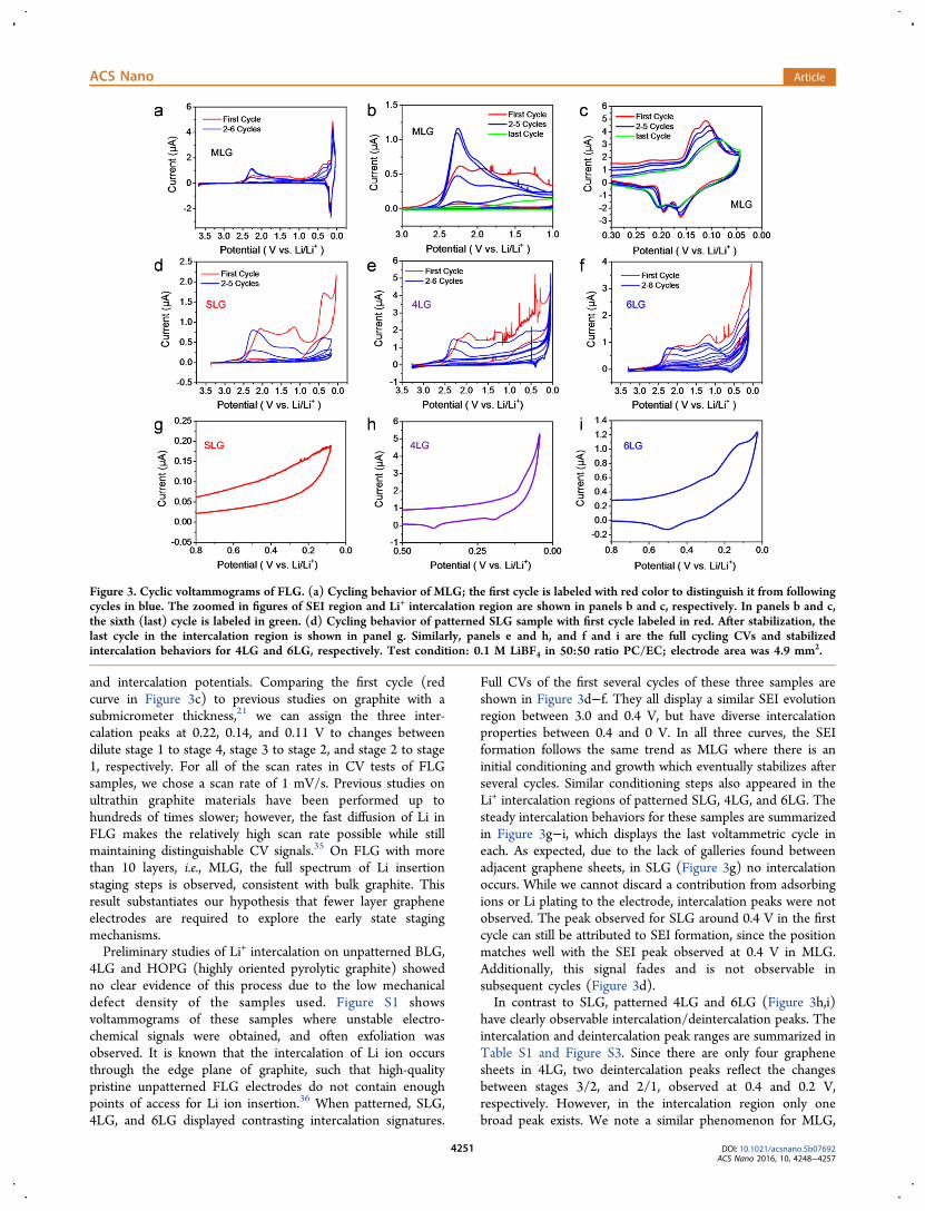
and intercalation potentials. Comparing the first cycle (redcurve in Figure 3c) to previous studies on graphite with asubmicrometer thickness,21 we can assign the three inter-calation peaks at 0.22, 0.14, and 0.11 V to changes betweendilute stage 1 to stage 4, stage 3 to stage 2, and stage 2 to stage1, respectively. For all of the scan rates in CV tests of FLGsamples, we chose a scan rate of 1 mV/s. Previous studies onultrathin graphite materials have been performed up tohundreds of times slower; however, the fast diffusion of Li inFLG makes the relatively high scan rate possible while stillmaintaining distinguishable CV signals.35 On FLG with morethan 10 layers, i.e., MLG, the full spectrum of Li insertionstaging steps is observed, consistent with bulk graphite. Thisresult substantiates our hypothesis that fewer layer grapheneelectrodes are required to explore the early state stagingmechanisms.Preliminary studies of Li+ intercalation on unpatterned BLG,
4LG and HOPG (highly oriented pyrolytic graphite) showedno clear evidence of this process due to the low mechanicaldefect density of the samples used. Figure S1 showsvoltammograms of these samples where unstable electro-chemical signals were obtained, and often exfoliation wasobserved. It is known that the intercalation of Li ion occursthrough the edge plane of graphite, such that high-qualitypristine unpatterned FLG electrodes do not contain enoughpoints of access for Li ion insertion.36 When patterned, SLG,4LG, and 6LG displayed contrasting intercalation signatures.
Full CVs of the first several cycles of these three samples areshown in Figure 3d−f. They all display a similar SEI evolutionregion between 3.0 and 0.4 V, but have diverse intercalationproperties between 0.4 and 0 V. In all three curves, the SEIformation follows the same trend as MLG where there is aninitial conditioning and growth which eventually stabilizes afterseveral cycles. Similar conditioning steps also appeared in theLi+ intercalation regions of patterned SLG, 4LG, and 6LG. Thesteady intercalation behaviors for these samples are summarizedin Figure 3g−i, which displays the last voltammetric cycle ineach. As expected, due to the lack of galleries found betweenadjacent graphene sheets, in SLG (Figure 3g) no intercalationoccurs. While we cannot discard a contribution from adsorbingions or Li plating to the electrode, intercalation peaks were notobserved. The peak observed for SLG around 0.4 V in the firstcycle can still be attributed to SEI formation, since the positionmatches well with the SEI peak observed at 0.4 V in MLG.Additionally, this signal fades and is not observable insubsequent cycles (Figure 3d).In contrast to SLG, patterned 4LG and 6LG (Figure 3h,i)
have clearly observable intercalation/deintercalation peaks. Theintercalation and deintercalation peak ranges are summarized inTable S1 and Figure S3. Since there are only four graphenesheets in 4LG, two deintercalation peaks reflect the changesbetween stages 3/2, and 2/1, observed at 0.4 and 0.2 V,respectively. However, in the intercalation region only onebroad peak exists. We note a similar phenomenon for MLG,
Figure 3. Cyclic voltammograms of FLG. (a) Cycling behavior of MLG; the first cycle is labeled with red color to distinguish it from followingcycles in blue. The zoomed in figures of SEI region and Li+ intercalation region are shown in panels b and c, respectively. In panels b and c,the sixth (last) cycle is labeled in green. (d) Cycling behavior of patterned SLG sample with first cycle labeled in red. After stabilization, thelast cycle in the intercalation region is shown in panel g. Similarly, panels e and h, and f and i are the full cycling CVs and stabilizedintercalation behaviors for 4LG and 6LG, respectively. Test condition: 0.1 M LiBF4 in 50:50 ratio PC/EC; electrode area was 4.9 mm2.
ACS Nano Article
DOI: 10.1021/acsnano.5b07692ACS Nano 2016, 10, 4248−4257
4251
shown in Figure 3c, in which the two intercalation peaks at 0.14and 0.11 V (red curve) gradually merge into one broad peak(green curve). Consequently, the two intercalation peaks in4LG could presumably also combine into one signal. However,the reason for this merging of peaks might be of differentorigin. In MLG at least, the evolution of intercalation peakssuggests that it might come from a conditioning of the material,where structural changes induced by multiple Li ion insertionsand extractions lead to a distribution of intercalation sites.When the direction of the potential sweep is reversed, the backdiffusion and deintercalation of Li ion is largely controlled bythe intrinsic properties of the already lithiated grapheneelectrode, thus yielding discrete deintercalation peaks. As thelayer number of graphene is increased to 6 layers, there aresufficient graphene sheets for all four staging states to beobserved.From Table S1 and Figure 3c,h,i, we noticed a continuous
shift of first and second deintercalation peaks among 4LG, 6LG,and MLG. Assuming MLG represents mostly bulk graphite’sproperties, the positive potential shifts at 4LG and 6LG mightcome from the effect of SEI/graphene and graphene/substrateinterface. The chemical environment induced by these twointerfaces might shift the energetics of the deintercalationprocess. As shown schematically in Figure S2, the impact ofthese interfaces decreases as FLG transitions into MLG byforming a better-defined bulk. We also note that differences inthe background currents in Figure 3c,g−i, likely result fromdifferent contributions of each sample to their capacitivecurrent and from residual SEI growth. SLG showed the lowestbackground current, reflecting its lowest activity towardreaction with Li and its lowest density of states whichcontribute to its capacitance. 4LG, 6LG, and MLG displayed
a similar background current of 0.8, 0.3, and ca. 1.0 μA,respectively, which was observed to decrease with an increasingcycling number.We note that the observed peaks in 6LG are broader than
those in 4LG. We believe this is a consequence of the broaderrange of configurations and interactions available with agrowing number of layers. Observing a progressive change isimportant in the context of the effects that turbostratic disorder,i.e., random rotations and translations on pairs of graphenelayers, potentially brings to the response of the lithiumintercalation signal.20 In the layer-by-layer transfer procedureused here, it is difficult to control turbostratic disorder;however, we believe that the existence of such disorder doesnot preclude the validity of the number of layer dependentobservations done here. In the first place, 4LG and 6LGsamples displayed marked voltammetric differences as afunction of the number of layers, despite being producedusing a common building material, i.e., bilayer graphene. Even ifthe galleries formed by the layer-by-layer transfer stacking oftwo BLG sheets were less active than the ones formed by thenative BLG, ionic interactions between Li+ ions would still beexpected to occur and to affect the electrostatic interactionsperpendicular to the surface. Second, lithiation is capable ofinducing the restacking of layers, provided the material iscapable of accommodating the necessary structuralchanges.20,37 As observed during our transfer procedure,“peeling off” of monolayer graphene is possible; thus, ourlayers are probably less bound than on natural graphite. Thismight facilitate structural changes after a few lithiation cyclesand relieve some of the original turbostratic disorder. Finally,turbostratic disorder has been shown to strongly impact theamount of Li+ that can be intercalated on carbons. The
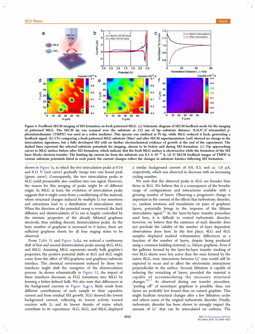
Figure 4. Feedback SECM imaging of SEI formation on fresh patterned MLG. (a) Schematic diagram of SECM feedback mode for the imagingof patterned MLG. The SECM tip was scanned over the substrate at 133 nm of tip−substrate distance. N,N,N′,N′-tetramethyl p-phenylenediamine (TMPD) was used as a redox mediator. This species was oxidized at Pt tip, while MLG reduced it back, generating afeedback signal. (b) CVs comparing a fresh patterned MLG substrate (blue) and after SECM experimentation (red) showed no change in theintercalation signatures, but a fully developed SEI with no further electrochemical evidence of growth at the end of the experiment. Thedashed lines represent the selected substrate potentials for imaging, chosen to be before and during SEI formation. (c) Tip approachingcurves to MLG surface before/after SEI formation, which indicate that the fresh MLG surface is electroactive while the formation of the SEIlayer blocks electron transfer. The limiting tip current far from the substrate was 9.3 × 10⁻¹⁰ A. (d−f) SECM feedback images of TMPD atvarious substrate potentials listed in each panel; the current changes reflect the changes in substrate kinetics following SEI formation.
ACS Nano Article
DOI: 10.1021/acsnano.5b07692ACS Nano 2016, 10, 4248−4257
4252
integrated charge of the deintercalation peaks in Figure 3h,i,shown in detail in Figure S3 and Table S1, yields theequivalents of Li+ diffused into FLG planes. 4LG yielded adeintercalation charge of 12.2 μC (85% of calculated theoreticalcharge), and 6LG has 15.7 μC (65% of calculated theoreticalcharge). Both figures show evidence for a largely lithiatedinterface. Even with a relatively fast scan rate and turbostraticdisordered structures, FLG can still maintain enough ability forLi insertion.19,20,38 The observations provided in this article seta precedent in which new mechanistic insights derived from thetransition of bulk graphite to an atomically thin interface can beexplored.In addition to its intercalation behavior, it is instructive to
explore the similarities and differences in the electronic andionic surface reactivity of graphene in the context of our currentunderstanding of carbon materials. Specifically, we addressedthe evolution of SEI conductivity and the role of the fabricatedionic-channels in facilitating Li ion intercalation. For thispurpose, we used scanning electrochemical microscopy, aversatile tool for detecting reactivity at operating electrodes. Tofurther explore the properties of the SEI, SECM operated in thefeedback mode (Figure 4a) was used to image the spatiallyresolved rate of electron transfer of a patterned MLG electrodeat various stages of SEI formation. According to the CVs ofFLG (Figure 3), all electrodes displayed qualitatively the sameSEI evolution process. Because MLG gave larger intercalationsignatures, this electrode was chosen as representative of FLGsamples to study SEI properties. When a nanodimensionedSECM tip was first approached to a pristine substrate ofpatterned multilayer graphene, positive feedback was observed,indicating that the substrate was electronically conductive, evenat open circuit when unbiased (Figure 4c, black curve). SECM
imaging was performed at various substrate potentials toobserve the feedback response as a function of electrodeactivation.Open circuit SECM images (Esub ∼ 3.3 V vs Li/Li+) revealed
nanoresolved features on the surface with clearly identifiablecircular patterns on the substrate that correspond perfectly tothe fabricated graphene patterns observed under SEM with thesame center to center distances for the holes. SECM imageswere collected at progressively more negative substratepotentials at a tip−substrate distance of 133 nm. As pointedout through the dashed lines in Figure 4b, we chose conditionsbefore, during, and after SEI formation, at 2.6, 1.2, and 0.07 Vvs Li/Li+, respectively. The SECM image at Esub of 2.6 V(Figure 4d) shows good contrast between patterned holes andthe MLG surface, with some contrast at defective regions thatrespond more to substrate overpotential. These defect regionshave faster electron transfer kinetics than pristine graphene andhave been observed previously via SECM39 and with dropletbased SECM probes.40
In following images, the substrate potential was ramped morenegatively, now forming an SEI, which progressively showed adecreasing tip feedback response due to decreased substratekinetics (Figure 4e,f). An overall decrease in tip currentobserved starting at Esub of 1.2 V (Figure 4e) suggests theformation of a homogeneous SEI layer that partially hinderselectron transfer at MLG surface. At Esub of 0.07 V (Figure 4f),the pattern was indistinguishable, yielding only negativefeedback to the tip signal. Negative feedback suggests aslowed-down regeneration of the mediator, indicative oflowered substrate kinetics that are unable to keep up withthe mass transport imposed by the tip. We note that the impactof the SEI on electron transfer is opposite to that expected by a
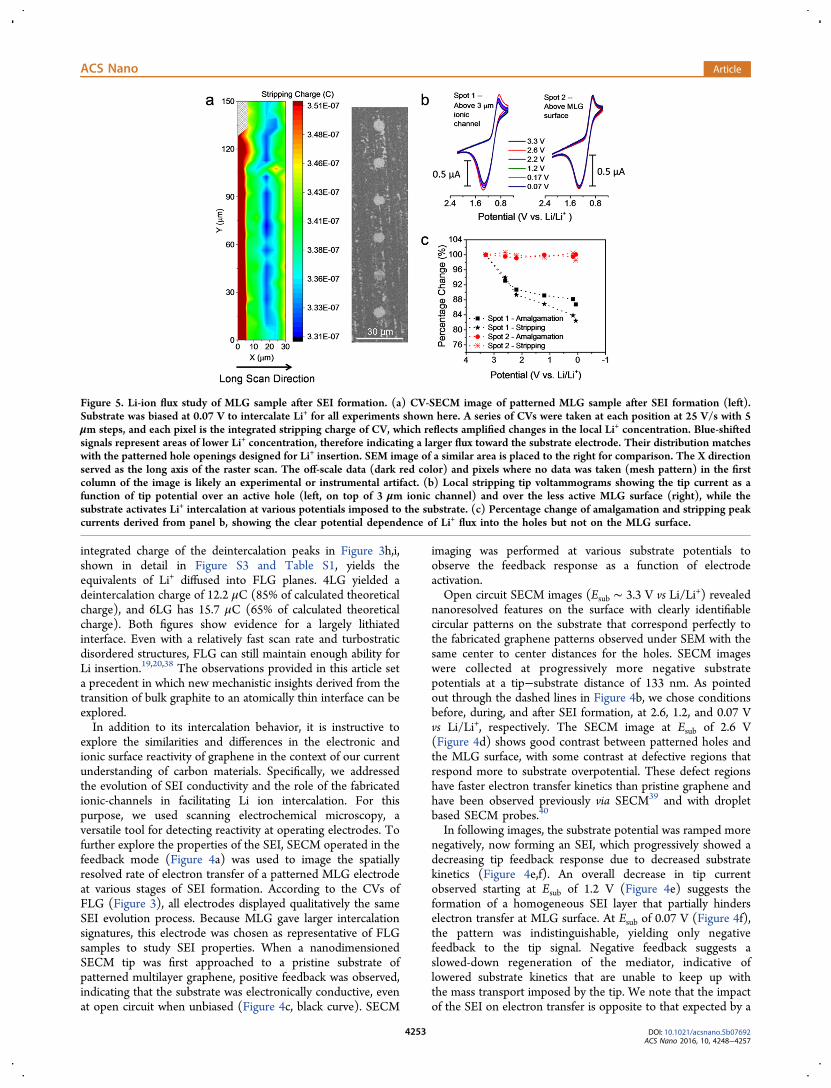
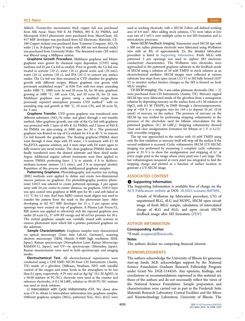
Figure 5. Li-ion flux study of MLG sample after SEI formation. (a) CV-SECM image of patterned MLG sample after SEI formation (left).Substrate was biased at 0.07 V to intercalate Li+ for all experiments shown here. A series of CVs were taken at each position at 25 V/s with 5μm steps, and each pixel is the integrated stripping charge of CV, which reflects amplified changes in the local Li+ concentration. Blue-shiftedsignals represent areas of lower Li+ concentration, therefore indicating a larger flux toward the substrate electrode. Their distribution matcheswith the patterned hole openings designed for Li+ insertion. SEM image of a similar area is placed to the right for comparison. The X directionserved as the long axis of the raster scan. The off-scale data (dark red color) and pixels where no data was taken (mesh pattern) in the firstcolumn of the image is likely an experimental or instrumental artifact. (b) Local stripping tip voltammograms showing the tip current as afunction of tip potential over an active hole (left, on top of 3 μm ionic channel) and over the less active MLG surface (right), while thesubstrate activates Li+ intercalation at various potentials imposed to the substrate. (c) Percentage change of amalgamation and stripping peakcurrents derived from panel b, showing the clear potential dependence of Li+ flux into the holes but not on the MLG surface.
ACS Nano Article
DOI: 10.1021/acsnano.5b07692ACS Nano 2016, 10, 4248−4257
4253
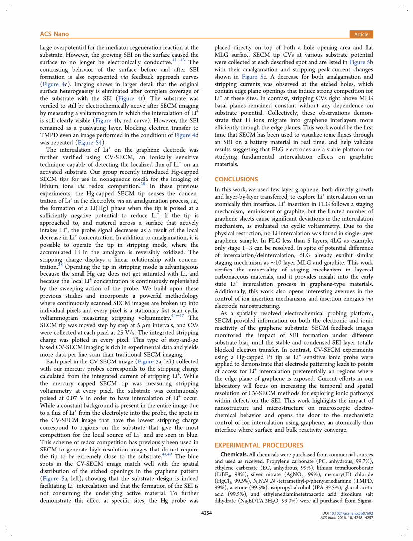
large overpotential for the mediator regeneration reaction at thesubstrate. However, the growing SEI on the surface caused thesurface to no longer be electronically conductive.41−43 Thecontrasting behavior of the surface before and after SEIformation is also represented via feedback approach curves(Figure 4c). Imaging shows in larger detail that the originalsurface heterogeneity is eliminated after complete coverage ofthe substrate with the SEI (Figure 4f). The substrate wasverified to still be electrochemically active after SECM imagingby measuring a voltammogram in which the intercalation of Li+
is still clearly visible (Figure 4b, red curve). However, the SEIremained as a passivating layer, blocking electron transfer toTMPD even an image performed in the conditions of Figure 4dwas repeated (Figure S4).The intercalation of Li+ on the graphene electrode was
further verified using CV-SECM, an ionically sensitivetechnique capable of detecting the localized flux of Li+ on anactivated substrate. Our group recently introduced Hg-cappedSECM tips for use in nonaqueous media for the imaging oflithium ions via redox competition.28 In these previousexperiments, the Hg-capped SECM tip senses the concen-tration of Li+ in the electrolyte via an amalgamation process, i.e.,the formation of a Li(Hg) phase when the tip is poised at asufficiently negative potential to reduce Li+. If the tip isapproached to, and rastered across a surface that activelyintakes Li+, the probe signal decreases as a result of the localdecrease in Li+ concentration. In addition to amalgamation, it ispossible to operate the tip in stripping mode, where theaccumulated Li in the amalgam is reversibly oxidized. Thestripping charge displays a linear relationship with concen-tration.28 Operating the tip in stripping mode is advantageousbecause the small Hg cap does not get saturated with Li, andbecause the local Li+ concentration is continuously replenishedby the sweeping action of the probe. We build upon theseprevious studies and incorporate a powerful methodologywhere continuously scanned SECM images are broken up intoindividual pixels and every pixel is a stationary fast scan cyclicvoltammogram measuring stripping voltammetry.44−47 TheSECM tip was moved step by step at 5 μm intervals, and CVswere collected at each pixel at 25 V/s. The integrated strippingcharge was plotted in every pixel. This type of stop-and-gobased CV-SECM imaging is rich in experimental data and yieldsmore data per line scan than traditional SECM imaging.Each pixel in the CV-SECM image (Figure 5a, left) collected
with our mercury probes corresponds to the stripping chargecalculated from the integrated current of stripping Li+. Whilethe mercury capped SECM tip was measuring strippingvoltammetry at every pixel, the substrate was continuouslypoised at 0.07 V in order to have intercalation of Li+ occur.While a constant background is present in the entire image dueto a flux of Li+ from the electrolyte into the probe, the spots inthe CV-SECM image that have the lowest stripping chargecorrespond to regions on the substrate that give the mostcompetition for the local source of Li+ and are seen in blue.This scheme of redox competition has previously been used inSECM to generate high resolution images that do not requirethe tip to be extremely close to the substrate.48,49 The bluespots in the CV-SECM image match well with the spatialdistribution of the etched openings in the graphene pattern(Figure 5a, left), showing that the substrate design is indeedfacilitating Li+ intercalation and that the formation of the SEI isnot consuming the underlying active material. To furtherdemonstrate this effect at specific sites, the Hg probe was
placed directly on top of both a hole opening area and flatMLG surface. SECM tip CVs at various substrate potentialwere collected at each described spot and are listed in Figure 5bwith their amalgamation and stripping peak current changesshown in Figure 5c. A decrease for both amalgamation andstripping currents was observed at the etched holes, whichcontain edge plane openings that induce strong competition forLi+ at these sites. In contrast, stripping CVs right above MLGbasal planes remained constant without any dependence onsubstrate potential. Collectively, these observations demon-strate that Li ions migrate into graphene interlayers moreefficiently through the edge planes. This work would be the firsttime that SECM has been used to visualize ionic fluxes throughan SEI on a battery material in real time, and help validateresults suggesting that FLG electrodes are a viable platform forstudying fundamental intercalation effects on graphiticmaterials.
CONCLUSIONS
In this work, we used few-layer graphene, both directly growthand layer-by-layer transferred, to explore Li+ intercalation on anatomically thin interface. Li+ insertion in FLG follows a stagingmechanism, reminiscent of graphite, but the limited number ofgraphene sheets cause significant deviations in the intercalationmechanism, as evaluated via cyclic voltammetry. Due to thephysical restriction, no Li intercalation was found in single-layergraphene sample. In FLG less than 5 layers, 4LG as example,only stage 1−3 can be resolved. In spite of potential differenceof intercalation/deintercalation, 6LG already exhibit similarstaging mechanism as ∼10 layer MLG and graphite. This workverifies the universality of staging mechanism in layeredcarbonaceous materials, and it provides insight into the earlystate Li+ intercalation process in graphene-type materials.Additionally, this work also opens interesting avenues in thecontrol of ion insertion mechanisms and insertion energies viaelectrode nanostructuring.As a spatially resolved electrochemical probing platform,
SECM provided information on both the electronic and ionicreactivity of the graphene substrate. SECM feedback imagesmonitored the impact of SEI formation under differentsubstrate bias, until the stable and condensed SEI layer totallyblocked electron transfer. In contrast, CV-SECM experimentsusing a Hg-capped Pt tip as Li+ sensitive ionic probe wereapplied to demonstrate that electrode patterning leads to pointsof access for Li+ intercalation preferentially on regions wherethe edge plane of graphene is exposed. Current efforts in ourlaboratory will focus on increasing the temporal and spatialresolution of CV-SECM methods for exploring ionic pathwayswithin defects on the SEI. This work highlights the impact ofnanostructure and microstructure on macroscopic electro-chemical behavior and opens the door to the mechanisticcontrol of ion intercalation using graphene, an atomically thininterface where surface and bulk reactivity converge.
EXPERIMENTAL PROCEDURESChemicals. All chemicals were purchased from commercial sources
and used as received. Propylene carbonate (PC, anhydrous, 99.7%),ethylene carbonate (EC, anhydrous, 99%), lithium tetrafluoroborate(LiBF4, 98%), silver nitrate (AgNO3, 99%), mercury(II) chloride(HgCl2, 99.5%), N,N,N′,N′-tetramethyl-p-phenylenediamine (TMPD,99%), acetone (99.5%), isopropyl alcohol (IPA 99.5%), glacial aceticacid (99.5%), and ethylenediaminetetraacetic acid disodium saltdihydrate (Na2EDTA·2H2O, 99.0%) were all purchased from Sigma-
ACS Nano Article
DOI: 10.1021/acsnano.5b07692ACS Nano 2016, 10, 4248−4257
4254
Aldrich. Twenty-five micrometers thick copper foil was purchasedfrom Alfa Aesar. Nano 950 K A4 PMMA, 495 K A2 PMMA, andMicroposit S1813 photoresist were purchased from MicroChem. AZ917 MIF developer was purchased from AZ Electronic Materials. CE-100 Copper etchant was purchased from Transene Company. SiO2/Siwafer (3 in. B-doped P-type Si wafer with 300 nm wet thermal oxide)was purchased from University Wafer. The deionized water (DI water)was filtered using a Millipore system.Graphene Growth Procedure. Multilayer graphene and bilayer
graphene were grown by chemical vapor deposition (CVD) usingmethane and 25 μm Cu foil as catalyst. Prior to growth, the Cu foil wastreated in acetone (10 s), water (10 s), glacial acetic acid (10 min),water (10 s), acetone (10 s), and IPA (10 s) to remove any surfaceoxides. The Cu foil was then mounted in CVD chamber for graphenegrowth with different recipes. Bilayer graphene was grown withpreviously established recipe50 at 0.04 Torr with two steps: annealingunder 1000 °C, 1000 sccm Ar and 50 sccm H2 for 30 min; graphenegrowing at 1000 °C, 100 sccm CH4 and 50 sccm H2 for 25 min.Multilayer graphene was grown using a modified recipe frompreviously reported atmosphere pressure CVD method51 with noannealing step and growth at 960 °C, 10 sccm CH4 and 30 sccm H2for 5 min.Graphene Transfer. CVD grown graphene was transferred onto
different substrates (SiO2/Si wafer, and glass) through a wet transfermethod. After graphene growth, one side of the Cu foil with graphenewas protected with 1 layer of 495 K A2 PMMA and 2 layers of 950 KA4 PMMA via spin-coating at 3000 rpm for 30 s. The protectedgraphene was floated on top of Cu etchant for 4 h at 40 °C to removeCu foil beneath the graphene. The floating graphene/PMMA sheetwent through 4 rinse steps with DI water, 1 h treatment with 0.1 MNa2EDTA aqueous solution, and 4 rinse steps with DI water again tofully remove any metal residue. The clean graphene/PMMA sheet wasfinally transferred onto the desired substrate and blow dried underArgon. Additional organic solvent treatments were then applied toremove PMMA protecting layer: 2 h in anisole, 4 h in dichloro-methane/acetone mixture (1:1 ratio), and 2 h in isopropyl alcohol.Repetition of this process yields multilayered graphene samples.Patterning Graphene. Photolithography and reactive ion etching
(RIE) methods were applied to define and create two-dimensionalmicron patterns on graphene. For photolithography, positive photo-resist S1813 was selected to create patterned openings, 3 μm squarearray with 24 μm center-to-center distance, on graphene. S1813 layerwas spin coated onto graphene at 4000 rpm for 45 s and soft baked at115 °C for 1.5 min. Karl Suss MJB3 contact mask aligner was used totransfer the pattern from the mask to the photoresist layer. Afterdeveloping in AZ 917 MIF developer for 15 s, 3 μm square arrayopenings were created on top of graphene. A Plasma Lab Freon/O2RIE system was applied to selectively etch the exposed graphene areaunder 20 sccm O2, 37 mW RF energy and 40 mTorr pressure for 30 s.The etched graphene sample was carefully rinsed with acetone toremove photoresist layer which left a pristine patterned graphene onthe substrate.Sample Characterization. Graphene samples were characterized
via optical microscopy (Zeiss Axio Lab.A1, Germany), scanningelectron microscopy (SEM, Hitachi S-4800 high resolution SEM,Japan), Raman spectroscopy (Nanophoton Laser Raman MicroscopeRAMAN-11, Japan), and UV−vis spectroscopy (Shimadzu, Japan).Raman measurements were used in both spectroscopic and imagingmodes.Electrochemical Test. All electrochemical experiments were
conducted using a CHI 920D SECM from CH Instruments (Austin,TX) inside of a glovebox (MBraun, Stratham, NH) with mindfulcontrol of the oxygen and water levels in the atmosphere to be lessthan 0.1 ppm, respectively. A Pt wire and an Ag/Ag+ (0.1 M AgNO3 ina 50:50 mixture of PC/EC) electrode were used as the counter andreference electrodes. A 0.1 M LiBF4 solution in 50:50 PC/EC mixturewas used as stock solution.Li Intercalation with Cyclic Voltammetry (CV). We chose slow
scan CV to obtain Li intercalation information into graphene samples.Different graphene samples (MLG, patterned SLG, 4LG, 6LG) were
used as working electrode, with a SECM Teflon cell defined workingarea of 4.9 mm2. After adding stock solution, CVs were taken at lowscan rate of 1 mV/s over multiple cycles to test SEI formation and Liintercalation processes.
Nano-SECM Feedback Imaging. Nanometer sized SECM tips witha 300 nm radius platinum electrode were fabricated using Wollastonwire with an RG of approximately 25; the detailed fabricationprocedure is listed in Supporting Information. Fresh MLG withpatterned 3 μm openings was used to explore SEI electronicconductivity characteristics. The Wollaston wire electrodes wereapproached to the patterned graphene substrate in the feedback modeof SECM using a solution of 10 mM TMPD in stock solution as anelectrochemical mediator. SECM images were collected at varioussubstrate bias steps from open circuit (3.3 V) to SEI fully formed (0.07V) to monitor surface kinetics changes as the SEI is formed on freshMLG samples.
CV-SECM Imaging. The 5 μm radius platinum electrodes (RG ∼ 2)were purchased from CH Instruments (Austin, TX). Mercury cappedSECM tips were fabricated inside of the glovebox from a nonaqeuoussolution by depositing mercury on the surface from a 0.1 M solution ofHgCl2 with 0.1 M TBAPF6 in DMF through a chronoamperometricstep at −0.8 V vs a tungsten wire for 144 s to deposit 34 μC (0.34nmol) of mercury on the surface. The presence of mercury on theSECM tip was verified by performing stripping voltammetry in thepresence of the electrolyte used for lithium intercalation for thepatterned graphene (0.1 M LiBF4). Stripping voltammetry showedclean and clear amalgamation formation for lithium at 1 V vs Li/Li+
with reversible stripping.The tip was approached to the surface with 10 mM TMPD using
only the first oxidation as mercury itself will strip off the surface if thesecond oxidation is accessed. Cyclic voltammetry SECM (CV-SECM)imaging was performed by measuring 3 complete cyclic voltammo-grams at 25 V/s to show the amalgamation and stripping of Li+ atevery single pixel in the image where every pixel was 5 μm large. Thelast voltammogram measured at every pixel was integrated to find thestripping charge and plotted as a function of surface location togenerate a CV-SECM image.
ASSOCIATED CONTENT*S Supporting InformationThe Supporting Information is available free of charge on theACS Publications website at DOI: 10.1021/acsnano.5b07692.
Details of Wollaston tip fabrication procedure, CVs ofunpatterned BLG, 4LG and HOPG, SECM open circuitimage of fresh MLG sample, calculation of intercalatedcharge of 4LG and 6LG, and open circuit SECMfeedback image after SEI formation (PDF)
AUTHOR INFORMATIONCorresponding Author*E-mail: [email protected] authors declare no competing financial interest.
ACKNOWLEDGMENTSThe authors acknowledge the University of Illinois for generousstart-up funds. M.B. acknowledges support by the NationalScience Foundation Graduate Research Fellowship Programunder Grant No. DGE-1144245. Any opinions, findings, andconclusions or recommendations expressed in this material arethose of the authors and do not necessarily reflect the views ofthe National Science Foundation. Sample preparation andcharacterization were carried out in part in the Frederick SeitzMaterials Research Laboratory Central Facilities and the Microand Nanotechnology Laboratory, University of Illinois. The
ACS Nano Article
DOI: 10.1021/acsnano.5b07692ACS Nano 2016, 10, 4248−4257
4255
authors would like to thank our group member Zachary J.Barton, for help in developing the implementation of theemployed CV-SECM technique.
REFERENCES(1) Yazami, R.; Touzain, P. A Reversible Graphite Lithium NegativeElectrode for Electrochemical Generators. J. Power Sources 1983, 9,365−371.(2) Levi, M. D.; Aurbach, D. The Mechanism of LithiumIntercalation in Graphite Film Electrodes in Aprotic Media. Part 1.High Resolution Slow Scan Rate Cyclic Voltammetric Studies andModeling. J. Electroanal. Chem. 1997, 421, 79−88.(3) Levi, M. D.; Levi, E. A.; Aurbach, D. The Mechanism of LithiumIntercalation in Graphite Film Electrodes in Aprotic Media. Part 2.Potentiostatic Intermittent Titration and in situ XRD Studies of theSolid-State Ionic Diffusion. J. Electroanal. Chem. 1997, 421, 89−97.(4) Verma, P.; Maire, P.; Novak, P. A Review of the Features andAnalyses of the Solid Electrolyte Interphase in Li-Ion Batteries.Electrochim. Acta 2010, 55, 6332−6341.(5) Agubra, V. A.; Fergus, J. W. The Formation and Stability of theSolid Electrolyte Interface on the Graphite Anode. J. Power Sources2014, 268, 153−162.(6) Zhang, S.; Ding, M. S.; Xu, K.; Allen, J.; Jow, T. R. UnderstandingSolid Electrolyte Interface Film Formation on Graphite Electrodes.Electrochem. Solid-State Lett. 2001, 4, A206−A208.(7) Herstedt, M.; Stjerndahl, M.; Gustafsson, T.; Edstrom, K. AnionReceptor for Enhanced Thermal Stability of the Graphite AnodeInterface in a Li-Ion Battery. Electrochem. Commun. 2003, 5, 467−472.(8) Aurbach, D.; Markovsky, B.; Weissman, I.; Levi, E.; Ein-Eli, Y. Onthe Correlation Between Surface Chemistry and Performance ofGraphite Negative Electrodes for Li Ion Batteries. Electrochim. Acta1999, 45, 67−86.(9) Etacheri, V.; Marom, R.; Elazari, R.; Salitra, G.; Aurbach, D.Challenges in the Development of Advanced Li-Ion Batteries: aReview. Energy Environ. Sci. 2011, 4, 3243−3262.(10) Petnikota, S.; Rotte, N.; Srikanth, V. S. S.; Kota, B. R.; Reddy,M. V.; Loh, K.; Chowdari, B. V. R. Electrochemical Studies of Few-Layered Graphene as an Anode Material for Li Ion Batteries. J. SolidState Electrochem. 2014, 18, 941−949.(11) Pollak, E.; Geng, B.; Jeon, K.-J.; Lucas, I. T.; Richardson, T. J.;Wang, F.; Kostecki, R. The Interaction of Li+ with Single-Layer andFew-Layer Graphene. Nano Lett. 2010, 10, 3386−3388.(12) Lee, E.; Persson, K. A. Li Absorption and Intercalation in SingleLayer Graphene and Few Layer Graphene by First Principles. NanoLett. 2012, 12, 4624−4628.(13) Liang, Y. T.; Hersam, M. C. Towards Rationally DesignedGraphene-Based Materials and Devices. Macromol. Chem. Phys. 2012,213, 1091−1100.(14) Geim, A. K. Graphene: Status and Prospects. Science 2009, 324,1530−1534.(15) Geim, A. K.; Novoselov, K. S. The Rise of Graphene. Nat.Mater. 2007, 6, 183−191.(16) Liao, L.; Peng, H.; Liu, Z. Chemistry Makes Graphene beyondGraphene. J. Am. Chem. Soc. 2014, 136, 12194−12200.(17) Dahn, J. R. Phase Diagram of LixC6. Phys. Rev. B: Condens.Matter Mater. Phys. 1991, 44, 9170−9177.(18) Song, M. K.; Hong, S. D.; No, K. T. The Structure of LithiumIntercalated Graphite Using an Effective Atomic Charge of Lithium. J.Electrochem. Soc. 2001, 148, A1159−A1163.(19) Zheng, T.; Dahn, J. R. Effect of Turbostratic Disorder on theStaging Phase Diagram of Lithium-Intercalated Graphitic CarbonHosts. Phys. Rev. B: Condens. Matter Mater. Phys. 1996, 53, 3061−3071.(20) Zheng, T.; Reimers, J. N.; Dahn, J. R. Effect of TurbostraticDisorder in Graphitic Carbon Hosts on the Intercalation of Lithium.Phys. Rev. B: Condens. Matter Mater. Phys. 1995, 51, 734−741.(21) Levi, M. D.; Aurbach, D. Simultaneous Measurements andModeling of the Electrochemical Impedance and the Cyclic
Voltammetric Characteristics of Graphite Electrodes Doped withLithium. J. Phys. Chem. B 1997, 101, 4630−4640.(22) Ritzert, N. L.; Rodriguez-Lopez, J.; Tan, C.; Abruna, H. D.Kinetics of Interfacial Electron Transfer at Single-Layer GrapheneElectrodes in Aqueous and Nonaqueous Solutions. Langmuir 2013, 29,1683−1694.(23) Eshkenazi, V.; Peled, E.; Burstein, L.; Golodnitsky, D. XPSAnalysis of the SEI Formed on Carbonaceous Materials. Solid StateIonics 2004, 170, 83−91.(24) Lee, J. T.; Nitta, N.; Benson, J.; Magasinski, A.; Fuller, T. F.;Yushin, G. Comparative Study of the Solid Electrolyte Interphase onGraphite in Full Li-Ion Battery Cells Using X-Ray PhotoelectronSpectroscopy, Secondary Ion Mass Spectrometry, and ElectronMicroscopy. Carbon 2013, 52, 388−397.(25) Santner, H. J.; Korepp, C.; Winter, M.; Besenhard, J. O.; Moller,K. C. In-situ FTIR Investigations on the Reduction of VinyleneElectrolyte Additives Suitable for Use in Lithium-Ion Batteries. Anal.Bioanal. Chem. 2004, 379, 266−271.(26) Chattopadhyay, S.; Lipson, A. L.; Karmel, H. J.; Emery, J. D.;Fister, T. T.; Fenter, P. A.; Hersam, M. C.; Bedzyk, M. J. In Situ X-rayStudy of the Solid Electrolyte Interphase (SEI) Formation onGraphene as a Model Li-ion Battery Anode. Chem. Mater. 2012, 24,3038−3043.(27) Zhang, S. S.; Xu, K.; Jow, T. R. EIS Study on the Formation ofSolid Electrolyte Interface in Li-Ion Battery. Electrochim. Acta 2006,51, 1636−1640.(28) Barton, Z. J.; Rodriguez-Lopez, J. Lithium Ion QuantificationUsing Mercury Amalgams as in Situ Electrochemical Probes inNonaqueous Media. Anal. Chem. 2014, 86, 10660−10667.(29) Graf, D.; Molitor, F.; Ensslin, K.; Stampfer, C.; Jungen, A.;Hierold, C.; Wirtz, L. Spatially Resolved Raman Spectroscopy ofSingle- and Few-Layer Graphene. Nano Lett. 2007, 7, 238−242.(30) Li, X. S.; Cai, W. W.; An, J. H.; Kim, S.; Nah, J.; Yang, D. X.;Piner, R.; Velamakanni, A.; Jung, I.; Tutuc, E.; Banerjee, S. K.;Colombo, L.; Ruoff, R. S. Large-Area Synthesis of High-Quality andUniform Graphene Films on Copper Foils. Science 2009, 324, 1312−1314.(31) Bae, S.; Kim, H.; Lee, Y.; Xu, X.; Park, J.-S.; Zheng, Y.;Balakrishnan, J.; Lei, T.; Ri Kim, H.; Song, Y. I.; Kim, Y.-J.; Kim, K. S.;Ozyilmaz, B.; Ahn, J.-H.; Hong, B. H.; Iijima, S. Roll-to-RollProduction of 30-in. Graphene Films for Transparent Electrodes.Nat. Nanotechnol. 2010, 5, 574−578.(32) Nair, R. R.; Blake, P.; Grigorenko, A. N.; Novoselov, K. S.;Booth, T. J.; Stauber, T.; Peres, N. M. R.; Geim, A. K. Fine StructureConstant Defines Visual Transparency of Graphene. Science 2008, 320,1308.(33) Ishigami, M.; Chen, J. H.; Cullen, W. G.; Fuhrer, M. S.;Williams, E. D. Atomic Structure of Graphene on SiO2. Nano Lett.2007, 7, 1643−1648.(34) Nie, M.; Chalasani, D.; Abraham, D. P.; Chen, Y.; Bose, A.;Lucht, B. L. Lithium Ion Battery Graphite Solid Electrolyte InterphaseRevealed by Microscopy and Spectroscopy. J. Phys. Chem. C 2013, 117,1257−1267.(35) Sole, C.; Drewett, N. E.; Liu, F.; Abdelkader, A. M.; Kinloch, I.A.; Hardwick, L. J. The Role of Re-Aggregation on the Performance ofElectrochemically Exfoliated Many-Layer Graphene for Li-IonBatteries. J. Electroanal. Chem. 2015, 753, 35−41.(36) Yamada, Y.; Miyazaki, K.; Abe, T. Role of Edge Orientation inKinetics of Electrochemical Intercalation of Lithium-Ion at Graphite.Langmuir 2010, 26, 14990−14994.(37) Boehm, R. C.; Banerjee, A. Theoretical Study of LithiumIntercalated Graphite. J. Chem. Phys. 1992, 96, 1150−1157.(38) Dahn, J. R.; Sleigh, A. K.; Shi, H.; Reimers, J. N.; Zhong, Q.;Way, B. M. Dependence of the Electrochemical Intercalation ofLithium in Carbons on the Crystal-Structure of the Carbon.Electrochim. Acta 1993, 38, 1179−1191.(39) Tan, C.; Rodríguez-Lopez, J.; Parks, J. J.; Ritzert, N. L.; Ralph,D. C.; Abruna, H. D. Reactivity of Monolayer Chemical Vapor
ACS Nano Article
DOI: 10.1021/acsnano.5b07692ACS Nano 2016, 10, 4248−4257
4256
Deposited Graphene Imperfections Studied Using Scanning Electro-chemical Microscopy. ACS Nano 2012, 6, 3070−3079.(40) Guell, A. G.; Cuharuc, A. S.; Kim, Y. R.; Zhang, G. H.; Tan, S.Y.; Ebejer, N.; Unwin, P. R. Redox-Dependent Spatially ResolvedElectrochemistry at Graphene and Graphite Step Edges. ACS Nano2015, 9, 3558−3571.(41) Zampardi, G.; La Mantia, F.; Schuhmann, W. Determination ofthe Formation and Range of Stability of the SEI on Glassy Carbon byLocal Electrochemistry. RSC Adv. 2015, 5, 31166−31171.(42) Zampardi, G.; La Mantia, F.; Schuhmann, W. In-OperandoEvaluation of the Effect of Vinylene Carbonate on the InsulatingCharacter of the Solid Electrolyte Interphase. Electrochem. Commun.2015, 58, 1−5.(43) Zampardi, G.; Ventosa, E.; La Mantia, F.; Schuhmann, W. InSitu Visualization of Li-Ion Intercalation and Formation of the SolidElectrolyte Interphase on TiO2 Based Paste Electrodes Using ScanningElectrochemical Microscopy. Chem. Commun. 2013, 49, 9347−9349.(44) Alpuche-Aviles, M. A.; Baur, J. E.; Wipf, D. O. Imaging of MetalIon Dissolution and Electrodeposition by Anodic StrippingVoltammetry-Scanning Electrochemical Microscopy. Anal. Chem.2008, 80, 3612−3621.(45) Diaz-Ballote, L.; Alpuche-Aviles, M.; Wipf, D. O. Fast-ScanCyclic Voltammetry-Scanning Electrochemical Microscopy. J. Elec-troanal. Chem. 2007, 604, 17−25.(46) Chen, C. H.; Jacobse, L.; McKelvey, K.; Lai, S. C. S.; Koper, M.T. M.; Unwin, P. R. Voltammetric Scanning Electrochemical CellMicroscopy: Dynamic Imaging of Hydrazine Electro-oxidation onPlatinum Electrodes. Anal. Chem. 2015, 87, 5782−5789.(47) Takahashi, Y.; Kumatani, A.; Munakata, H.; Inomata, H.; Ito, K.;Ino, K.; Shiku, H.; Unwin, P. R.; Korchev, Y. E.; Kanamura, K.;Matsue, T. Nanoscale Visualization of Redox Activity at Lithium-IonBattery Cathodes. Nat. Commun. 2014, 5, 5450.(48) Eckhard, K.; Chen, X. X.; Turcu, F.; Schuhmann, W. RedoxCompetition Mode of Scanning Electrochemical Microscopy (RC-SECM) for Visualisation of Local Catalytic Activity. Phys. Chem. Chem.Phys. 2006, 8, 5359−5365.(49) Zoski, C. G.; Aguilar, J. C.; Bard, A. J. Scanning ElectrochemicalMicroscopy. 46. Shielding Effects on Reversible and QuasireversibleReactions. Anal. Chem. 2003, 75, 2959−2966.(50) Cristarella, T. C.; Chinderle, A. J.; Hui, J.; Rodríguez-Lopez, J.Single-Layer Graphene as a Stable and Transparent Electrode forNonaqueous Radical Annihilation Electrogenerated Chemilumines-cence. Langmuir 2015, 31, 3999−4007.(51) Tu, Z.; Liu, Z.; Li, Y.; Yang, F.; Zhang, L.; Zhao, Z.; Xu, C.; Wu,S.; Liu, H.; Yang, H.; Richard, P. Controllable Growth of 1−7 Layersof Graphene by Chemical Vapour Deposition. Carbon 2014, 73, 252−258.
ACS Nano Article
DOI: 10.1021/acsnano.5b07692ACS Nano 2016, 10, 4248−4257
4257