Embed Size (px)
Citation preview
Probing the spatial and momentum distribution of confined surface states in a metal coordination network Jun Zhang,a Aneliia Shchyrba,b Sylwia Nowakowska,b Ernst Meyer,b Thomas A. Jungb,c,* and Matthias Muntwilera,*
aLaboratory for Synchrotron Radiation – Condensed Matter, Paul Scherrer Institute, 5232 Villigen PSI, Switzerland. bDepartment of Physics, University of Basel, Klingelbergstrasse 82, 4056 Basel, Switzerland.
cLaboratory for Micro- and Nanotechnology, Paul Scherrer Institute, 5232 Villigen PSI, Switzerland.
1. Experimental methodsThe experiment was carried out in an Omicron low temperature scanning tunneling microscope system. The Cu(111) substrate was cleaned by repeated cycles of Ar+ ions sputtering and annealing at ~800 K. DCA molecules were deposited by thermal evaporation while the substrate was kept at room temperature (for the porous adatom coordinated network) or low temperature ~100 K (for closely packed molecular domains). STM measurements were performed at liquid helium temperature (~4.7 K) with a PtIr tip or a tungsten tip. The bias voltages referred to in all the figures are sample voltages.
The Scanning Tunneling Spectroscopy (STS) data and dI/dV (differential conductance) maps are acquired under open feedback loop conditions by using a lock-in amplifier with a modulation voltage of 10 mV or 30 mV (rms) at 662.5 Hz. The set point before switching off the feedback loop is -1.0 V or -0.5 V, and the tunneling current varies from 70 pA to 250 pA. dI/dV maps are extracted from a set of 110 × 91 (Fig. 1(c)) or 130 × 118 (Fig. 3(a-e)) point spectra taken across the area of interest. The intensity of the spectra of the dI/dV map is normalized to the signal intensity between -0.5 V and -0.45 V, where there is no special feature on the spectra taken within molecular domains. To acquire a set of spectra takes 8 to 17 hours, therefore the shown maps are slightly distorted due to drift. Line scans of differential conductance spectra are extracted from a set of 70~150 point spectra, depending on the range of the line scan, and are normalized to the signal intensity between -1.0 V and -0.9 V.
2. Complementary STM data to Fig. 1 in the manuscript
Fig. S1 Molecule manipulation process. (a,b) STM images of the same position taken with the same tunneling condition (1.0 V, 1.0 nA, 8.6 nm × 8.6 nm) before and after molecule manipulation. Along the arrow shown in (a), a line scan with reduced tunneling junction (1 mV, 4 nA) is performed to transfer the molecule from the substrate to STM tip. The white circle marked in the images shows the position where the molecule disappears after manipulation. The enhanced resolution of the tip after manipulation is attributed to the modified electronic state properties of the tip by the molecule.
Electronic Supplementary Material (ESI) for ChemComm.This journal is © The Royal Society of Chemistry 2014
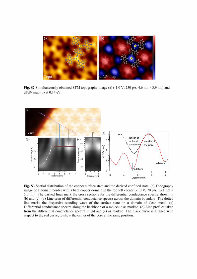
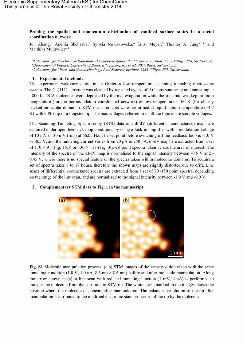
Fig. S2 Simultaneously obtained STM topography image (a) (-1.0 V, 250 pA, 4.6 nm × 3.9 nm) and dI/dV map (b) at 0.14 eV.
Fig. S3 Spatial distribution of the copper surface state and the derived confined state. (a) Topography image of a domain border with a bare copper domain in the top left corner (-1.0 V, 70 pA, 13.1 nm × 5.0 nm). The dashed lines mark the cross sections for the differential conductance spectra shown in (b) and (c). (b) Line scan of differential conductance spectra across the domain boundary. The dotted line marks the dispersive standing wave of the surface state on a domain of clean metal. (c) Differential conductance spectra along the backbone of a molecule as marked. (d) Line profiles taken from the differential conductance spectra in (b) and (c) as marked. The black curve is aligned with respect to the red curve, to show the center of the pore at the same position.
3. STS on closely packed molecular domainThe spectrum taken on a molecule in the closely packed domain is shown for comparison (Fig. S4). The absence of the surface state related feature indicates that the DCA molecules quench the intrinsic surface state of the Cu(111) substrate.
Fig. S4 Quenching of the surface state in the closely packed DCA domain. (a) Large scale STM image of the closely packed molecular structure (-1.0 V, 10 pA, 50 nm × 50 nm). In this case, molecules are deposited on the Cu(111) substrate which is kept at ~100 K with no adatoms available. (b) High resolution image (0.1 V, 200 pA, 5.1 nm × 5.1 nm) measured with a DCA modified tip. A molecular structure model is superimposed. (c) STS performed on a molecule (red curve) and on Cu(111) (black curve). The red spot marked in the inset image (-1.0 V, 15 pA, 15 nm × 12 nm) shows the position where the spectrum has been taken. The surface state shows some feature on Cu(111) due to the one-dimensional confinement caused by the molecular structures.
4. Analysis of the molecular adsorption configuration at domain boundary regionBetween two molecules across the domain boundary, the intensity for the confined states is always lower than on the molecular backbone (see Fig. 3). Here, the confined state is detectable in similar magnitude as measured at the adatom positions in the coordination network. Therefore, we suggest that also at the domain boundary region, CN groups are coordinated with Cu adatoms. Considering the directional character of the coordination bond, the adsorption site of the adatoms and the symmetry of the structure in STM image, we propose a model with one adatom involved in the coordination of boundary molecules as shown in Fig. S5(b) where the adatom adsorbs at a bridge site. Alternatively, Fig. S5(c-d) shows two possible configurations involving two adatoms. In these cases, the adatoms adsorb near bridge sites, which may increase the energy of the system. Based on these simple arguments, we expect the structure in Fig. S5(b) to be more stable, however, further measurements and calculations are needed to reach a conclusion. Since the exact configuration does
not significantly influence the analysis of the confined state, we have used the configuration shown in Fig. S5(b) to develop the following structural models.
Fig. S5 Adsorption configuration of molecules at a domain boundary region. (a) High resolution STM image of the domain boundary region with one of the proposed assembly structure superimposed (-0.5 V, 100 pA, 7.5 nm × 4.5 nm). Proposed models with one (b) or two (c-d) adatoms involved in the coordination of boundary molecules.
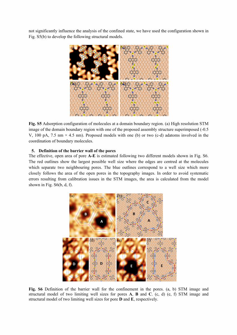
5. Definition of the barrier wall of the poresThe effective, open area of pore A-E is estimated following two different models shown in Fig. S6. The red outlines show the largest possible well size where the edges are centred at the molecules which separate two neighbouring pores. The blue outlines correspond to a well size which more closely follows the area of the open pores in the topography images. In order to avoid systematic errors resulting from calibration issues in the STM images, the area is calculated from the model shown in Fig. S6(b, d, f).
Fig. S6 Definition of the barrier wall for the confinement in the pores. (a, b) STM image and structural model of two limiting well sizes for pores A, B and C. (c, d) (e, f) STM image and structural model of two limiting well sizes for pore D and E, respectively.
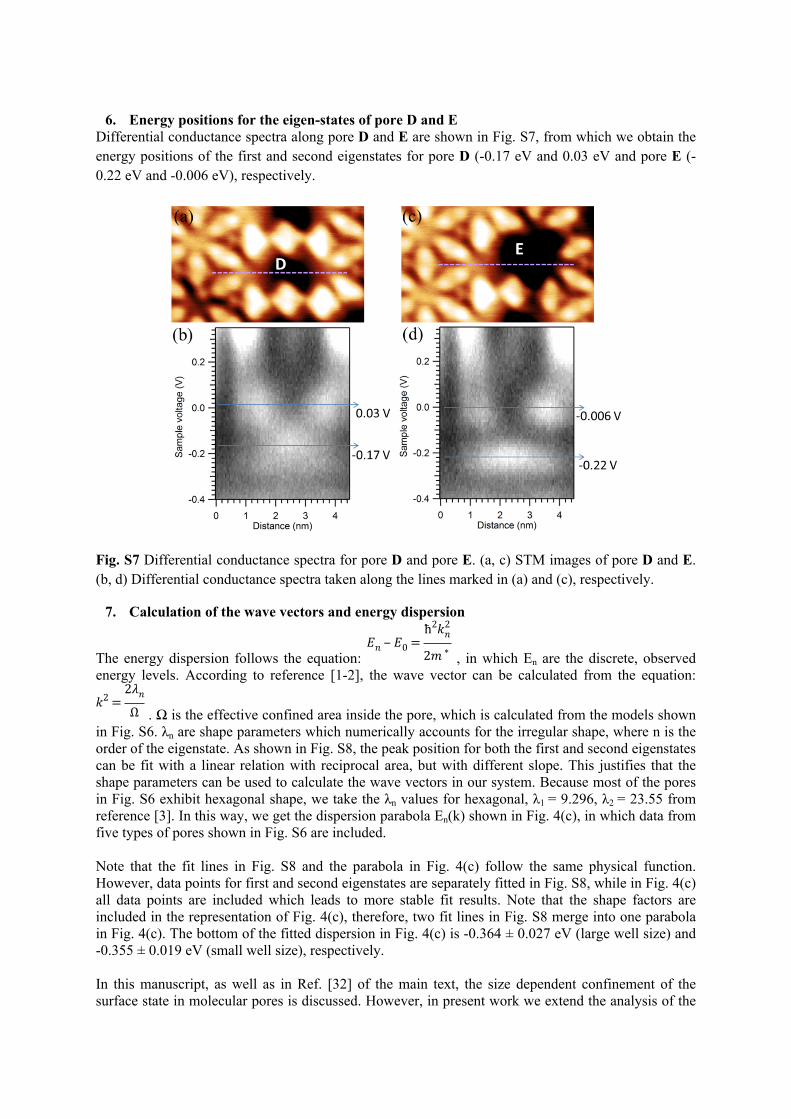
6. Energy positions for the eigen-states of pore D and E Differential conductance spectra along pore D and E are shown in Fig. S7, from which we obtain the energy positions of the first and second eigenstates for pore D (-0.17 eV and 0.03 eV and pore E (-0.22 eV and -0.006 eV), respectively.
Fig. S7 Differential conductance spectra for pore D and pore E. (a, c) STM images of pore D and E. (b, d) Differential conductance spectra taken along the lines marked in (a) and (c), respectively.
7. Calculation of the wave vectors and energy dispersion
The energy dispersion follows the equation: , in which En are the discrete, observed 𝐸𝑛 ‒ 𝐸0 =
ħ2𝑘2𝑛
2𝑚 ∗
energy levels. According to reference [1-2], the wave vector can be calculated from the equation:
. Ω is the effective confined area inside the pore, which is calculated from the models shown 𝑘2 =
2𝜆𝑛
Ωin Fig. S6. λn are shape parameters which numerically accounts for the irregular shape, where n is the order of the eigenstate. As shown in Fig. S8, the peak position for both the first and second eigenstates can be fit with a linear relation with reciprocal area, but with different slope. This justifies that the shape parameters can be used to calculate the wave vectors in our system. Because most of the pores in Fig. S6 exhibit hexagonal shape, we take the λn values for hexagonal, λ1 = 9.296, λ2 = 23.55 from reference [3]. In this way, we get the dispersion parabola En(k) shown in Fig. 4(c), in which data from five types of pores shown in Fig. S6 are included.
Note that the fit lines in Fig. S8 and the parabola in Fig. 4(c) follow the same physical function. However, data points for first and second eigenstates are separately fitted in Fig. S8, while in Fig. 4(c) all data points are included which leads to more stable fit results. Note that the shape factors are included in the representation of Fig. 4(c), therefore, two fit lines in Fig. S8 merge into one parabola in Fig. 4(c). The bottom of the fitted dispersion in Fig. 4(c) is -0.364 ± 0.027 eV (large well size) and -0.355 ± 0.019 eV (small well size), respectively.
In this manuscript, as well as in Ref. [32] of the main text, the size dependent confinement of the surface state in molecular pores is discussed. However, in present work we extend the analysis of the
confinement effect and address the influence of the effective confinement area Ω on the analysis of effective mass of the electron m*. Moreover, our reciprocal space analysis allows us to derive the shift of the surface state band bottom upon confinement (see Fig. 4(c) and main text of the manuscript), which might not be accessed in the irregular/aperiodic molecular on-surface systems by e.g. ARPES.
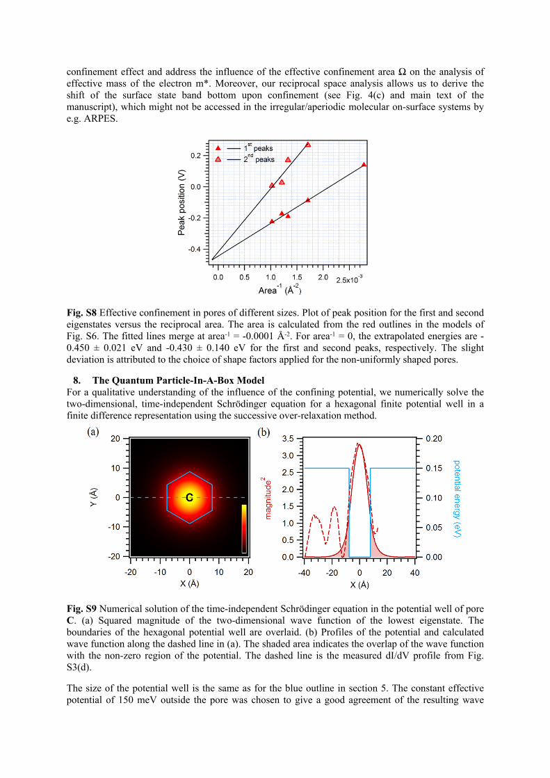
Fig. S8 Effective confinement in pores of different sizes. Plot of peak position for the first and second eigenstates versus the reciprocal area. The area is calculated from the red outlines in the models of Fig. S6. The fitted lines merge at area-1 = -0.0001 Å-2. For area-1 = 0, the extrapolated energies are -0.450 ± 0.021 eV and -0.430 ± 0.140 eV for the first and second peaks, respectively. The slight deviation is attributed to the choice of shape factors applied for the non-uniformly shaped pores.
8. The Quantum Particle-In-A-Box ModelFor a qualitative understanding of the influence of the confining potential, we numerically solve the two-dimensional, time-independent Schrödinger equation for a hexagonal finite potential well in a finite difference representation using the successive over-relaxation method.
Fig. S9 Numerical solution of the time-independent Schrödinger equation in the potential well of pore C. (a) Squared magnitude of the two-dimensional wave function of the lowest eigenstate. The boundaries of the hexagonal potential well are overlaid. (b) Profiles of the potential and calculated wave function along the dashed line in (a). The shaded area indicates the overlap of the wave function with the non-zero region of the potential. The dashed line is the measured dI/dV profile from Fig. S3(d).
The size of the potential well is the same as for the blue outline in section 5. The constant effective potential of 150 meV outside the pore was chosen to give a good agreement of the resulting wave

function profile with measured data. The parameters shown here give a good qualitative match of the wave function with the measured dI/dV profile in section 2. Variations of the parameters and shape of the potential have a minor influence on the result than the spatial size of the potential well.
The shaded area in Fig. S9(b) shows the overlap of the wave function with the effective scattering potential of the molecular network. If we neglect the kinetic term of the Hamiltonian H at k|| = 0, the
expectation value reduces to the overlap integral which amounts to ~65 meV. ⟨𝐻⟩ ∫𝜓 ∗ 𝜓 𝑉(𝑥,𝑦) 𝑑𝑥 𝑑𝑦
1 J. Li, W.-D. Schneider, R. Berndt, and S. Crampin, Phys. Rev. Lett., 1998, 80, 3332–3335.
2 R. Temirov, S. Soubatch, A. Luican, and F. S. Tautz, Nature, 2006, 444, 350–3.
3 J. Li, W.-D. Schneider, S. Crampin, and R. Berndt, Surf. Sci., 1999, 422, 95–106.