Embed Size (px)
Citation preview

NJG1801K75
- 1 - Ver.2015-03-20
SPDT SWITCH GaAs MMIC GENERAL DESCRIPTION PACKAGE OUTLINE
The NJG1801K75 is a SPDT switch IC suited for switching transmit/receive signals at 802.11 a/b/g/n/ac applications. The NJG1801K75 features low insertion loss, high
isolation, and high handling power. This switch exhibits wide frequency coverage up to
6.0GHz. And the ultra small and ultra thin package of DFN6-75 is adopted.
APPLICATION 802.11 a/b/g/n/ac networks applications Transmit / receive switching, path switching applications
FEATURES
Control voltage VCTL(H)=3.0V typ.
VCTL(L)=0V typ.
Low insertion loss 0.35dB typ. @f=2.4 to 2.5GHz
0.45dB typ. @f=4.9 to 5.9GHz
High isolation 28dB typ. @f=2.4 to 2.5GHz
30dB typ. @f=4.9 to 5.9GHz
P-1dB P-1dB=31 dBm typ. @f=2.5GHz
P-1dB=31 dBm typ. @f=5.9GHz
Ultra small & ultra thin package DFN6-75 (Package Size: 1.0x1.0x0.375mm typ.) RoHS compliant and Halogen Free, MSL1
PIN CONFIGURATION
TRUTH TABLE
“H”=VCTL(H), “L”=VCTL(L)
ON PATH VCTL1 VCTL2
PC-P1 L H
PC-P2 H L
NOTE: Please note that any data or drawing in this catalog is subject to change.
NJG1801K75
Pin connection
1. P1
2. GND
3. P2
4. VCTL2
5. PC
6. VCTL1
(Top view)
NJG1801K75
- 2 -
ABSOLUTE MAXIMUM RATINGS
Ta=+25°C, ZS=Zl=50 Ω
PARAMETER SYMBOL CONDITIONS RATINGS UNITS
RF Input Power PIN VCTL(L)=0V,VCTL(H)=3.0V, ON State Port
+31 dBm
Control Voltage VCTL 6.0 V
Power Dissipation PD 4-layer FR4 PCB without through-hole (76.2x114.3mm), Tj=150°C
430 mW
Operating Temperature Topr -40 to +105 °C
Storage Temperature Tstg -55 to +150 °C
ELECTRICAL CHARACTERISTICS1 (DC CHARACTERISTICS)
(General conditions: VCTL(H)=3.0V, VCTL(L)=0V,Ta=+25°C, with application circuit)
PARAMETERS SYMBOL CONDITIONS MIN TYP MAX UNITS
Control Voltage (HIGH) VCTL(H) 1.8 3.0 5.0 V
Control Voltage (LOW) VCTL(L) -0.2 - 0.2 V
Control Current ICTL - 5 10 µA

NJG1801K75
- 3 -
ELECTRICAL CHARACTERISTICS2 (RF CHARACTERISTICS)
(General conditions: VCTL(H)=3.0V, VCTL(L)=0V, Ta=+25°C, ZS=Zl=50 Ω, with application circuit)
PARAMETERS SYMBOL CONDITIONS MIN TYP MAX UNITS
Insertion loss1 LOSS1 f=2.4 to 2.5GHz - 0.35 0.55 dB
Insertion loss2 LOSS2 f=4.9 to 5.9GHz - 0.45 0.70 dB
Isolation1 ISL1 f=2.4 to 2.5GHz 25 28 - dB
Isolation2 ISL2 f=4.9 to 5.9GHz 25 30 - dB
Return loss1 RL1 f=2.4 to 2.5GHz 18 28 - dB
Return loss2 RL2 f=4.9 to 5.9GHz 15 20 - dB
Input power at 1dB compression point1
P-1dB1 f=2.4 to 2.5GHz 29 31 - dBm
Input power at 1dB compression point2
P-1dB2 f=4.9 to 5.9GHz 28 31 - dBm
Switching time TSW 50% VCTL to 10%/90% RF - 100 300 ns

NJG1801K75
- 4 -
TERMINAL INFORMATION
No. SYMBOL DESCRIPTION
1 P1 RF terminal. An external DC blocking capacitor is required.
2 GND Ground terminal. Please connect this terminal with ground plane as close as possible for excellent RF performance.
3 P2 RF terminal. An external DC blocking capacitor is required.
4 VCTL2 Control voltage input terminal.
5 PC Common RF terminal. An external DC blocking capacitor is required.
6 VCTL1 Control voltage input terminal.
NJG1801K75
- 5 -
ELECTRICAL CHARACTERISTICS
Loss, ISL vs Frequency(PC-P1 ON, VCTL(H)=3.0V, VCTL(L)=0V)
-2.0
-1.8
-1.6
-1.4
-1.2
-1.0
-0.8
-0.6
-0.4
-0.2
0.0
0.0 1.0 2.0 3.0 4.0 5.0 6.0
Frequency (GHz)
PC-P1 Insertion Loss (dB)
-40
-36
-32
-28
-24
-20
-16
-12
-8
-4
0
PC-P2 Isolation (dB)
Loss, ISL vs Frequency(PC-P2 ON, VCTL(H)=3.0V, VCTL(L)=0V)
-2.0
-1.8
-1.6
-1.4
-1.2
-1.0
-0.8
-0.6
-0.4
-0.2
0.0
0.0 1.0 2.0 3.0 4.0 5.0 6.0
Frequency (GHz)
PC-P2 Insertion Loss (dB)
-40
-36
-32
-28
-24
-20
-16
-12
-8
-4
0
PC-P1 Isolation (dB)
Return Loss vs Frequency(PC-P1 ON, VCTL(H)=3.0V, VCTL(L)=0V)
-50
-45
-40
-35
-30
-25
-20
-15
-10
-5
0
0.0 1.0 2.0 3.0 4.0 5.0 6.0
Frequency (GHz)
Return Loss (dB)
P1 port
PC port
Return Loss vs Frequency(PC-P2 ON, VCTL(H)=3.0V, VCTL(L)=0V)
-50
-45
-40
-35
-30
-25
-20
-15
-10
-5
0
0.0 1.0 2.0 3.0 4.0 5.0 6.0
Frequency (GHz)
Return Loss (dB)
P2 port
PC port
Arb. Unit
Time (400ns/div)
Switching Time(PC-P1 Path, VCTL(H)=3.0V, VCTL(L)=0V)
VCTL2
P1 Port
122ns
137ns

NJG1801K75
- 6 -
ELECTRICAL CHARACTERISTICS
8
10
12
14
16
18
20
22
24
26
28
30
32
0
2
4
6
8
10
12
14
16
18
20
22
24
10 12 14 16 18 20 22 24 26 28 30 32
VCTL(H)
=1.8V_POUT
VCTL(H)
=2.7V_POUT
VCTL(H)
=3.0V_POUT
VCTL(H)
=4.0V_POUT
VCTL(H)
=5.0V_POUT
VCTL(H)
=1.8V
VCTL(H)
=2.7V
VCTL(H)
=3.0V
VCTL(H)
=4.0V
VCTL(H)
=5.0V
Input Power (dBm)
Output Power (dBm)
Output Power, ICTL
vs Input Power(PC-P1 ON, V
CTL(L)=0V, f=2.5GHz)
Operation Current ICTL( µµ µµA)
-2.0
-1.8
-1.6
-1.4
-1.2
-1.0
-0.8
-0.6
-0.4
-0.2
0.0
-40
-36
-32
-28
-24
-20
-16
-12
-8
-4
0
10 12 14 16 18 20 22 24 26 28 30 32
VCTL(H)
=1.8V_Loss
VCTL(H)
=2.7V_Loss
VCTL(H)
=3.0V_Loss
VCTL(H)
=4.0V_Loss
VCTL(H)
=5.0V_Loss
VCTL(H)
=1.8V
VCTL(H)
=2.7V
VCTL(H)
=3.0V
VCTL(H)
=4.0V
VCTL(H)
=5.0V
Input Power (dBm)
PC-P1 Insertion Loss (dB)
PC-P2 Isolation (dB)
Loss, ISL vs Input Power
(PC-P1 ON, VCTL(L)
=0V, f=2.5GHz)
-2.0
-1.8
-1.6
-1.4
-1.2
-1.0
-0.8
-0.6
-0.4
-0.2
0.0
-40
-36
-32
-28
-24
-20
-16
-12
-8
-4
0
10 12 14 16 18 20 22 24 26 28 30 32
VCTL(H)
=1.8V_Loss
VCTL(H)
=2.7V_Loss
VCTL(H)
=3.0V_Loss
VCTL(H)
=4.0V_Loss
VCTL(H)
=5.0V_Loss
VCTL(H)
=1.8V
VCTL(H)
=2.7V
VCTL(H)
=3.0V
VCTL(H)
=4.0V
VCTL(H)
=5.0V
Input Power (dBm)
PC-P1 Insertion Loss (dB)
PC-P2 Isolation (dB)
Loss, ISL vs Input Power
(PC-P1 ON, VCTL(L)
=0V, f=5.9GHz)
8
10
12
14
16
18
20
22
24
26
28
30
32
0
2
4
6
8
10
12
14
16
18
20
22
24
10 12 14 16 18 20 22 24 26 28 30 32
VCTL(H)
=1.8V_POUT
VCTL(H)
=2.7V_POUT
VCTL(H)
=3.0V_POUT
VCTL(H)
=4.0V_POUT
VCTL(H)
=5.0V_POUT
VCTL(H)
=1.8V
VCTL(H)
=2.7V
VCTL(H)
=3.0V
VCTL(H)
=4.0V
VCTL(H)
=5.0V
Input Power (dBm)
Output Power (dBm)
Output Power, ICTL
vs Input Power(PC-P1 ON, V
CTL(L)=0V, f=5.9GHz)
Operation Current ICTL( µµ µµA)
Output Power, IM3 vs Input Power(PC-P1 ON, VCTL(H)=3.0V, VCTL(L)=0V, f=2.5GHz+2.501GHz)
-80
-60
-40
-20
0
20
40
60
80
10 20 30 40 50 60 70
Input Power (dBm)
Pout, IM3 (dBm)
Pout
IM3
IIP3=56.7dBm
0
10
20
30
40
50
60
70
17 18 19 20 21 22 23
VCTL(H)
=1.8V
VCTL(H)
=2.7V
VCTL(H)
=3.0V
VCTL(H)
=4.0V
VCTL(H)
=5.0V
IIP3 (dBm)
Input Power (dBm)
IIP3 vs Input Power(PC-P1 ON, V
CTL(L)=0V, f=2.5GHz+2.501GHz)

NJG1801K75
- 7 -
ELECTRICAL CHARACTERISTICS
0
1
2
3
4
5
6
7
8
9
10
8 10 12 14 16 18 20 22 24 26 28
THRUVCTL(H)
=1.8V
VCTL(H)
=2.2V
VCTL(H)
=2.7V
VCTL(H)
=3.0V
VCTL(H)
=4.0V
VCTL(H)
=5.0V
EVM (%
)
Input Power (dBm)
EVM vs Input Power(PC-P1 ON, V
CTL(L)=0V, f=2.5GHz, OFDM 64QAM)
0
1
2
3
4
5
6
7
8
9
10
8 10 12 14 16 18 20 22 24 26 28
THRUVCTL(H)
=1.8V
VCTL(H)
=2.2V
VCTL(H)
=2.7V
VCTL(H)
=3.0V
VCTL(H)
=4.0V
VCTL(H)
=5.0V
EVM (%
)
Input Power (dBm)
EVM vs Input Power(PC-P1 ON, V
CTL(L)=0V, f=5.9GHz, OFDM 64QAM)

NJG1801K75
- 8 -
ELECTRICAL CHARACTERISTICS
-2.0
-1.8
-1.6
-1.4
-1.2
-1.0
-0.8
-0.6
-0.4
-0.2
0.0
-40
-36
-32
-28
-24
-20
-16
-12
-8
-4
0
-50 -25 0 25 50 75 100 125
VCTL(H)
=1.8V_L
VCTL(H)
=2.7V_L
VCTL(H)
=3.0V_L
VCTL(H)
=4.0V_L
VCTL(H)
=5.0V_L
VCTL(H)
=1.8V
VCTL(H)
=2.7V
VCTL(H)
=3.0V
VCTL(H)
=4.0V
VCTL(H)
=5.0V
PC-P1 Insertion Loss (dB)
PC-P2 Isolation (dB)
Loss, ISL vs Temperature(PC-P1 ON, V
CTL(L)=0V, f=2.5GHz, P
IN=13dBm)
Ambient Temperature (oC)
-2.0
-1.8
-1.6
-1.4
-1.2
-1.0
-0.8
-0.6
-0.4
-0.2
0.0
-40
-36
-32
-28
-24
-20
-16
-12
-8
-4
0
-50 -25 0 25 50 75 100 125
VCTL(H)
=1.8V_L
VCTL(H)
=2.7V_L
VCTL(H)
=3.0V_L
VCTL(H)
=4.0V_L
VCTL(H)
=5.0V_L
VCTL(H)
=1.8V
VCTL(H)
=2.7V
VCTL(H)
=3.0V
VCTL(H)
=4.0V
VCTL(H)
=5.0V
PC-P1 Insertion Loss (dB)
PC-P2 Isolation (dB)
Loss, ISL vs Temperature(PC-P1 ON, V
CTL(L)=0V, f=5.9GHz, P
IN=13dBm)
Ambient Temperature (oC)
-40
-35
-30
-25
-20
-15
-10
-5
0
-50 -25 0 25 50 75 100 125
VCTL(H)
=1.8V
VCTL(H)
=2.7V
VCTL(H)
=3.0V
VCTL(H)
=4.0V
VCTL(H)
=5.0V
PC port Return Loss (dB)
Return Loss vs Temperature(PC-P1 ON, V
CTL(L)=0V, f=5.9GHz)
Ambient Temperature (oC)
-40
-35
-30
-25
-20
-15
-10
-5
0
-50 -25 0 25 50 75 100 125
VCTL(H)
=1.8V
VCTL(H)
=2.7V
VCTL(H)
=3.0V
VCTL(H)
=4.0V
VCTL(H)
=5.0V
PC port Return Loss (dB)
Return Loss vs Temperature(PC-P1 ON, V
CTL(L)=0V, f=2.5GHz)
Ambient Temperature (oC)
0
50
100
150
200
250
300
350
400
450
500
-50 -25 0 25 50 75 100 125
VCTL(H)
=1.8V
VCTL(H)
=2.7V
VCTL(H)
=3.0V
VCTL(H)
=4.0V
VCTL(H)
=5.0V
Switching Time (ns)
Switching Time(rise) vs Temperature(PC-P1 path, P1 port, V
CTL(L)=0V)
Ambient Temperature (oC)
10
12
14
16
18
20
22
24
26
28
30
32
34
-50 -25 0 25 50 75 100 125
VCTL(H)
=1.8V
VCTL(H)
=2.7V
VCTL(H)
=3.0V
VCTL(H)
=4.0V
VCTL(H)
=5.0V
P-1dB (dB)
P-1dB
vs Temperature
(PC-P1 ON, VCTL(L)
=0V, f=2.5GHz)
Ambient Temperature (oC)

NJG1801K75
- 9 -
APPLICATION CIRCUIT
RECOMMENDED PCB DESIGN
(TOP VIEW)
PARTS LIST
No. Value Notes
C1 to C3 27pF Murata MFG
(GRM03 series) C4 to C5 10pF
(TOP VIEW)
3
2
4
1
5
6 C1
C2
C3
C4
C5
P1
P2
PC
VCTL1
VCTL2
PCB: FR-4, t=0.2mm
Capacitor Size: 0603 (0.6 x 0.3 mm)
Strip Line Width: 0.4mm
PCB Size: 19.4 x 14.0mm
Through Hole Diameter: 0.2mm
Loss of PCB, capacitor and connectors
Frequency (GHz) Loss (dB)
2.4 0.33
2.5 0.34
4.9 0.55
5.9 0.65
VCTL2
PC
P2 P1 C1 C2
C3
VCTL1
GND
1pin mark
C4 C5

NJG1801K75
- 10 -
PCB LAYOUT GUIDELINE
(TOP VIEW)
PRECAUTIONS [1] The DC blocking capacitors should be placed at RF terminals. Please choose appropriate capacitance
value at the application frequency. [2] For good RF performance, exposed pad should be connected to PCB ground plane as close as possible.
1 2 3
4 5 6
GND Via Hole
Diameter φ= 0.2mm
PKG Terminal
PCB
PKG Outline
NJG1801K75
- 11 -
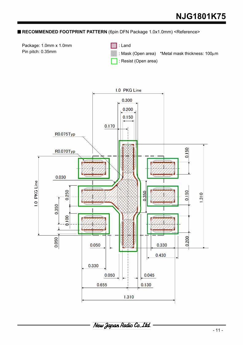
RECOMMENDED FOOTPRINT PATTERN (6pin DFN Package 1.0x1.0mm) <Reference>
Package: 1.0mm x 1.0mm
Pin pitch: 0.35mm
: Land
: Mask (Open area) *Metal mask thickness: 100µm
: Resist (Open area)
NJG1801K75
- 12 -
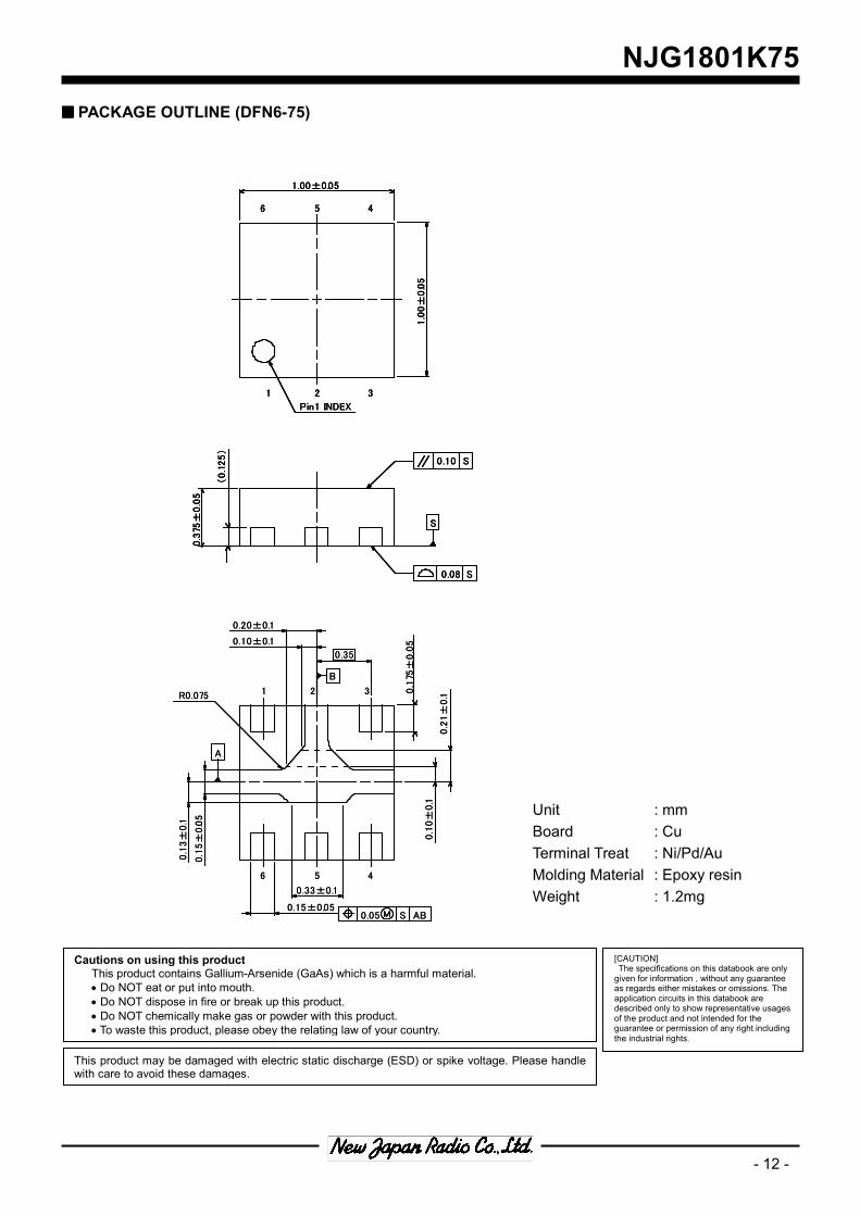
Unit : mm
Board : Cu
Terminal Treat : Ni/Pd/Au
Molding Material : Epoxy resin
Weight : 1.2mg
PACKAGE OUTLINE (DFN6-75)
Cautions on using this product This product contains Gallium-Arsenide (GaAs) which is a harmful material.
• Do NOT eat or put into mouth.
• Do NOT dispose in fire or break up this product.
• Do NOT chemically make gas or powder with this product.
• To waste this product, please obey the relating law of your country.
This product may be damaged with electric static discharge (ESD) or spike voltage. Please handle with care to avoid these damages.
[CAUTION] The specifications on this databook are only given for information , without any guarantee as regards either mistakes or omissions. The application circuits in this databook are described only to show representative usages of the product and not intended for the guarantee or permission of any right including
the industrial rights.
0.15±0.05
A
B
0.05 S AB
1
0.35
0.1
5±
0.0
5
0.1
75±
0.0
5
R0.075
0.33±0.1
0.1
3±
0.1
0.1
0±
0.1
0.2
1±
0.1
0.10±0.1
0.20±0.1
2 3
6 5 4
1.00±0.05
Pin1 INDEX
1 2 3
6 5 4
1.0
0±
0.0
5
S
0.08 S
0.10 S
0.3
75±
0.0
5
(0.1
25)
0.15±0.05
A
B
0.05 S AB
1
0.35
0.1
5±
0.0
5
0.1
75±
0.0
5
R0.075
0.33±0.1
0.1
3±
0.1
0.1
0±
0.1
0.2
1±
0.1
0.10±0.1
0.20±0.1
2 3
6 5 4
1.00±0.05
Pin1 INDEX
1 2 3
6 5 4
1.0
0±
0.0
5
1.00±0.05
Pin1 INDEX
1 2 3
6 5 4
1.0
0±
0.0
5
S
0.08 S
0.10 S
0.3
75±
0.0
5
(0.1
25)
S
0.08 S
0.10 S
0.3
75±
0.0
5
(0.1
25)