Embed Size (px)
Citation preview
Ninth Workshop on CrystallineSilicon Solar Cell Materialsand Processes
Summary Discussion Sessions
November 1999 • NREL/CP-520-27571
Workshop Chairman:Bhushan Sopori
Prepared By:Bhushan Sopori, Teh Tan, Dick Swanson,Mark Rosenblum and Ron Sinton
Workshop held at Beaver Run ResortBreckenridge, ColoradoAugust 9-11, 1999
National Renewable Energy Laboratory1617 Cole BoulevardGolden, Colorado 80401-3393NREL is a U.S. Department of Energy LaboratoryOperated by Midwest Research Institute •••• Battelle •••• Bechtel
Contract No. DE-AC36-99-GO10337
Ninth Workshop on CrystallineSilicon Solar Cell Materialsand Processes
Summary Discussion Sessions
November 1999 • NREL/CP-520-27571
Workshop Chairman:Bhushan Sopori
Prepared By:Bhushan Sopori, Teh Tan, Dick Swanson,Mark Rosenblum and Ron Sinton
Workshop held at Beaver Run ResortBreckenridge, ColoradoAugust 9-11, 1999Prepared under Task No. PV002501
National Renewable Energy Laboratory1617 Cole BoulevardGolden, Colorado 80401-3393NREL is a U.S. Department of Energy LaboratoryOperated by Midwest Research Institute •••• Battelle •••• Bechtel
Contract No. DE-AC36-99-GO10337
NOTICE
This report was prepared as an account of work sponsored by an agency of the United Statesgovernment. Neither the United States government nor any agency thereof, nor any of their employees,makes any warranty, express or implied, or assumes any legal liability or responsibility for the accuracy,completeness, or usefulness of any information, apparatus, product, or process disclosed, or representsthat its use would not infringe privately owned rights. Reference herein to any specific commercialproduct, process, or service by trade name, trademark, manufacturer, or otherwise does not necessarilyconstitute or imply its endorsement, recommendation, or favoring by the United States government or anyagency thereof. The views and opinions of authors expressed herein do not necessarily state or reflectthose of the United States government or any agency thereof.
Available electronically at http://www.doe.gov/bridge
Available for a processing fee to U.S. Department of Energyand its contractors, in paper, from:
U.S. Department of EnergyOffice of Scientific and Technical InformationP.O. Box 62Oak Ridge, TN 37831-0062phone: 865.576.8401fax: 865.576.5728email: [email protected]
Available for sale to the public, in paper, from:U.S. Department of CommerceNational Technical Information Service5285 Port Royal RoadSpringfield, VA 22161phone: 800.553.6847fax: 703.605.6900email: [email protected] ordering: http://www.ntis.gov/ordering.htm
Printed on paper containing at least 50% wastepaper, including 20% postconsumer waste
1
Executive Summary
The workshop was attended by 102 scientists, engineers, and students, which included 18international participants, working in the photovoltaic and microelectronics fields. The theme forthe workshop was: "R&D Challenges and Opportunities in Si Photovoltaics." This theme waschosen because it appropriately reflects a host of challenges that the growing production of Siphotovoltaics will be facing in the new millennium. The anticipated challenges will arise indeveloping strategies for cost reduction, increased production, higher throughput permanufacturing line, new sources of low-cost Si, and the introduction of new manufacturingprocesses for cell production. At the same time, technologies based on CdTe and CIS will comeon line posing new competition. With these challenges come new opportunities for Si PV towean itself from the microelectronics industry, to embark on a more aggressive program in thin-film Si solar cells, and to try new approaches to process monitoring.
The nine sessions held at the workshop included topics of immediate concern to the PVcommunity, such as: the mechanical properties of Si and how to address the issue of breakage ofthin Si wafers (a very important topic because industry is hoping to move into this area), thetechnical aspects of upgrading MG-Si, and process monitoring methods. Topics also includedthe more traditional areas such as impurity gettering and passivation, contacts to solar cells, andscience and engineering of defects in silicon. Also added to the agenda was the InternationalResearch Programs session. This session emphasized the need for international collaborations inareas that are somewhat less sensitive to proprietary issues.
Another change was added to this year's format—the traditional panel discussions werereplaced with "open discussions." These open discussions were moderated by two chairpersons.This change was aimed at increasing the discussion time to allow participants to bring out thescientific issues related to the sessions.
In an effort to assist graduate students with the expenses associated with attending theworkshop, four graduate students received monetary awards, which were sponsored by the PVindustry. The graduate students came from Pennsylvania State University, Georgia Tech, theUniversity of Arkansas, Little Rock, and Carnegie Mellon.
Perhaps the most noticeable feature of the workshop was a high degree of openness bymany industry participants (especially at the international level) that is typically absent in majorconferences.
2
Session 2. Poly Feedstock and Silicon Growth
Chairpersons: Ted Ciszek, National Renewable Energy LaboratoryKim Mitchell, Consultant
The discussion was preceded by two oral presentations by Chandra Khattak of Crystal
Systems (CS) and Fukuo Aratani of Kawaski Steel (NEDO). They addressed refinement of
metallurgical-grade Si into solar-grade (SOG) feedstock using their respective processes. The
majority of the discussion focussed on the details of these two processes. Each of these
processes uses refinement of molten Si as compared to the conventional chemical vapor process
for obtaining electronic-grade feedstock. The CS and NEDO processes basically produce little or
no chemical waste as compared to conventional processes that are more expensive and generate a
lot of chemical waste. The energy consumption in the NEDO process is ~70kWH/kg-Si during
the entire process that takes 12–15 h. The "maintaining" energy consumption of the CS process
is ~5-10 kWH/kg-Si for 8 h; there is no final energy consumption estimate because the process is
still under development. The melt-refining processes may be made more effective and efficient
if the incoming metallurgical-grade feedstock is a chlorosilane process. Both CS and Kawasaki
Steel hope to commercialize their processes.
Because the physics and the chemistry of some of the refining mechanisms are not well
understood, it was not obvious as to what the final achievable purity of the refined material can
be. As a result, there was a discussion of the mechanisms that limit the impurity refinement in
such a process. Some acceptable impurity specifications of SOG-Si feedstock are: 0.1 ppma for
B, Al, and P; 1 ppma for transition metals and C. It may require use of selected feedstock that
has a well-defined range of impurities to achieve these specifications. Thus, it may be necessary
to develop a test method to determine impurities in the SOG feedstock.
Other comments:
• The preferred price of SOG-Si is ~$13.00, which may be unrealistically low (e.g., the
estimated NEDO production cost is ~$20.00).
• It is believed that the supply of cheap feedstock, consisting of IC industry rejects, will run out
in Y2005.
• Feedstock is less of an issue for ribbon manufacturers than it is for the ingot growers.
3
Session 3. Impurities and Defects in PV-Si
Discussion Leaders: Eicke Weber, University of California, Berkeley Stefan Estreicher, Texas Tech University
Transition metals (TM), grain boundaries, dislocations/defect clusters, metal precipitates, and
even C and O are lifetime killers. NREL work has shown that defect clusters are preferred sites
for metal precipitation, and the dissolution of these precipitates does not occur during cell
fabrication. Theoretical work from Duke University has shown that high temperatures
(∼ 1200°C) and long times (many hours) are needed to dissolves precipitates of reasonable size.
These parameters depend on the composition and size of the precipitates. Therefore, structural
and chemical information is needed on the extended defects. LBNL work indicates that Fe
precipitates may not simply be silicides, but can also be silicates or oxides. If so, such
precipitates will be even more difficult to remove by gettering, because their solubility in the
dissolved phase is orders of magnitude lower than that of the silicides. Fe silicates and oxides
are insulators, and their electrical activity will be due to interface states, whereas that of silicide
precipitates will also have a Schottky component.
Injection of either the Si-self-interstitial or vacancy may enhance the dissolution of precipitate.
The kind of defects that can enhance dissolution of a particular precipitate depends on the
volume changes upon their dissolution. If the soluble phase requires volume expansion, the
dissolution will be enhanced by the injection of interstitials and retarded by the vacancies. In
multicrystalline Si substrates, the dislocations and grain boundaries will also compete for the in-
jected point-defect species. If the transition metal precipitates are indeed silicates and/or oxides,
then gettering based on the current approaches will not be helpful. In view of some successful
gettering experiments, even for very bad crystal regions, perhaps not all precipitates are silicates
or oxides.
Because high concentrations of impurities will always lead to their precipitation, and the
precipitated impurities are difficult to dissolve by post-growth processing, it is perhaps best to
reexamine the possibility of lowering the impurity content of low-cost single and multicrystalline
Si substrates. One may find that a slower growth can reject Fe and other transition metals (TM)
4
through segregation, yielding a higher quality material. Thus, it may be possible to trade growth
speed against TM content.
Session 4. Mechanical Properties of PV-Si
Discussion Leaders: Mark Rosenblum, ASE Americas, Inc. Dieter G. Ast, Cornell University
The discussion was preceded by two oral presentations by Terry Jester and Stephen Shea, who
covered the increasing yield losses encountered in processing thinner Si wafers. The discussion
started with an overview of mechanical issues (yield losses) and the associated cost concerns for
PV devices, by Mark Rosenblum. A mechanical-yield loss, caused by wafer cracking and
breakage, can lead to a significant increase in the cell cost. The PV industry currently accepts
5%–10% breakage. Because this is clearly too high (and is likely to increase when the thickness
of the wafers is reduced) it is important to investigate mechanisms of wafer breakage and
mitigate them.
This was followed by a theoretical overview of the fracture strength (resistance to fracture) of Si
by Dieter Ast. The fracture strength is largely determined by the edge quality. Fracture strength
= Kc/√(πa), where Kc is a material dependent parameter, and “a” is the length of microcracks at
the edges of the wafer. Because microcracks originate primarily from stress during cutting,
precutting processing such as annealing can reduce “a” and increase the fracture strength.
Alternately, etching can be used to reduce “a” and increase the fracture strength.
Wafer cracking and breakage starts with existing microcracks, situated on the wafer, produced
during crystal cutting/polishing (CZ) or cutting (ribbons) after growth. The microcracks widen
under a tensile stress generated during handling/processing. A chemical etch can remove these
cracks, but it is difficult to apply to multicrystalline wafers and ribbons because it can also lead to
grain boundary grooving. As the wafers get thin (e.g., from 250 down to ~150 µm) this becomes
a major problem. A milder cutting technique and/or annealing the wafers (to remove built-in
5
stress) can alleviate the problem, with the latter effect achieved by dislocation motion. With still
thinner wafer (e.g., 50 µm), the situation may become better because the wafer will become
easier to deform elastically. Dislocation motion is not effective in remedying the breakage
problem at T<600oC because dislocations are not usually mobile at these low temperatures.
The discussion proceeded as a series of questions and answers.
Q. Is wafer slicing the original source of cracks?
A. For wafers sliced from ingots, cracks generally originate from the grinding process. Some
PV companies already have specifications for surface finish, because there is a correlation to
breakage.
Q. What is the role of dislocations in crack propagation?
A. Dislocations in Si are not mobile at room temperature, except when the stress state is nearly
hydrostatically compressive. The stress field at a crack tip is mostly tensile, and fracture will
proceed long before significant dislocation movement occurs.
Q. Is there a critical thickness level below which the resistance to fracture actually improves?
A. In theory, the answer is no. It just takes more deflection of a wafer to build up enough stress
to break it, so it appears that thinner wafers have a higher fracture strength. However, because
resistance to bending is what is needed in practice in a cell fabrication line, better yields should
indeed be seen below some thickness value.
Comment: For Si, 50-µm thickness or less provides good flexibility.
Q. Do the nicks induced at the edges of wafers by wafer processing and handling follow the
theory presented earlier?
A. Yes. Nicks are essentially “notches,” and even 90° notches, with sharp bottoms, follow crack
theory to first order.
Q. What is the origin of residual stress?
A. Residual stress originates from the second derivative d2T/dx2 in the thermal profile.
6
Q. What is the influence of single crystal vs. polycrystalline Si fracture strength, everything else
being equal?
A. Polycrystalline Si would actually be better, because crack propagation can stop at a grain
boundary perpendicular to the propagation direction. In a single crystal, a force applied to a
crack would travel throughout the wafer.
Other comments:
• An Al BSF layer might actually be helpful here, as it could help straighten out the resulting
curved wafers.
• A 50-µm thick target for thin curved wafers (even if achieved by etching) would be better than
100 µm, because wafer elasticity would be exceptionally high: wafers can generally be flexed
easily without fracture. Also, mounting the finished cells on a metal substrate prior to lamination
would push the stress into the stronger substrate, reducing lamination breakage during module
fabrication.
• A SiN dielectric passivation layer for the back side, in place of an Al BSF layer, would
probably be a good solution to the warping encountered when Al is applied onto thin Si wafers.
Session 5. Passivation
Chairpersons: Michael Stavola, Lehigh University Jack Hanoka, Evergreen Solar, Inc.
The discussion ended up as a question and answer session following Brian Nielsen's talk on
hydrogen. A general feeling was that the structures of V-H related complexes, from VH to
V2H6, are now reasonably understood.
Q: Do V-H complexes help or hurt for introducing hydrogen into Si?
A. V and I may help to dissociate hidden hydrogen, possibly in the form of H2. V-H is not a fast
diffuser, but the liberated H atom should be.
Q. When H is introduced by SiNx deposition and cooled down, why doesn't one see B-acceptor
compensation?
7
A. B-H complexes are not stable at the processing temperature, and probably form H2. B-H
complexes would form only if the samples were quenched.
Q. What is the hydrogen concentration deep in the material, say 300 µm deep?
A. (i) Passivation of defects extends to hundreds of µm deep. (ii) SIMS data show H deeper than
50 µm in solar cells with concentrations of ~1015 cm-3.
Q and A related to Katsuhiko Shirasawa's talk on SiNx Passivation Process:
Q. How do maintenance and downtime compare for the SiN and TiO2 deposition machines ?
A. Maintenance for the TiO2 process is easy. For the SiNx process, many particles are produced.
The present deposition system has an up time of 80% (the goal is 90%).
Q. What is the refractive index of SiNx?
A. Two.
Q. A drawback of remote PECVD is that it requires frequent cleaning. How does this compare
to HWCVD?
A. No data for HWCVD, it is a research project. For the PECVD system. Five depositions are
done, followed by one cleaning cycle.
Q. What is the thickness of the deposited SiNx layer?
A. ~80 nm.
Q. What deposition temperatures are used?
A. T>400oC.
Q. What is the throughput of the current deposition system?
A. 900 wafers/h. The goal is to achieve 1800 wafers/h.
The session was closed with a host of open questions:
1. Passivation mechanism
• What are we learning about metal passivation?
• What is the dislocation passivation mechanism— clean vs. dirty dislocations?
• Can metal silicides be passivated?
8
2. How does H diffuse through solar cells?
• Seems to diffuse with isolated H atoms. Mechanism?
3. Where is H "stored" in dislocated Si? In what form? Can it be used later in subsequent
processes?
4. Different materials, mc-Si, CZ-Si, and FZ Si, show different passivation behavior. How is
this to be understood?
5. What is the best method of introducing H?
• SiNx appears to be the current favorite. How does it work? Source of H? Source of native
defects?
• H2 during growth? Forming gas annealing?
• Is there something inexpensive and clever that has been missed?
Comment: We have begun to understand the fundamental properties of H complexes with
"simple" defects in Si. We cannot yet answer questions for complicated systems and/or "dirty"
materials.
Session 6. Solar Cell Processing
Chairpersons: Johan Nijs, IMEC Jim Rand, AstroPower, Inc.
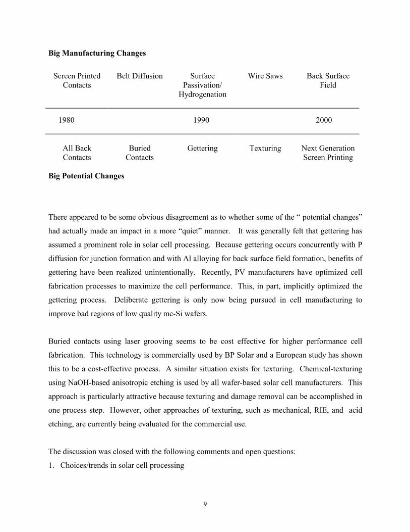
The discussion started with a diagram proposed by Rand, Fig. 1, which describes the
significant manufacturing process changes occurred in the last 20 years. Big Manufacturing
Changes are those adopted, while Big Potential Changes are those having potential but yet to
be adopted.
9
Big Manufacturing Changes
Screen PrintedContacts
Belt Diffusion SurfacePassivation/
Hydrogenation
Wire Saws Back SurfaceField
1980 1990 2000
All BackContacts
BuriedContacts
Gettering Texturing Next GenerationScreen Printing
Big Potential Changes
There appeared to be some obvious disagreement as to whether some of the “ potential changes”
had actually made an impact in a more “quiet” manner. It was generally felt that gettering has
assumed a prominent role in solar cell processing. Because gettering occurs concurrently with P
diffusion for junction formation and with Al alloying for back surface field formation, benefits of
gettering have been realized unintentionally. Recently, PV manufacturers have optimized cell
fabrication processes to maximize the cell performance. This, in part, implicitly optimized the
gettering process. Deliberate gettering is only now being pursued in cell manufacturing to
improve bad regions of low quality mc-Si wafers.
Buried contacts using laser grooving seems to be cost effective for higher performance cell
fabrication. This technology is commercially used by BP Solar and a European study has shown
this to be a cost-effective process. A similar situation exists for texturing. Chemical-texturing
using NaOH-based anisotropic etching is used by all wafer-based solar cell manufacturers. This
approach is particularly attractive because texturing and damage removal can be accomplished in
one process step. However, other approaches of texturing, such as mechanical, RIE, and acid
etching, are currently being evaluated for the commercial use.
The discussion was closed with the following comments and open questions:
1. Choices/trends in solar cell processing
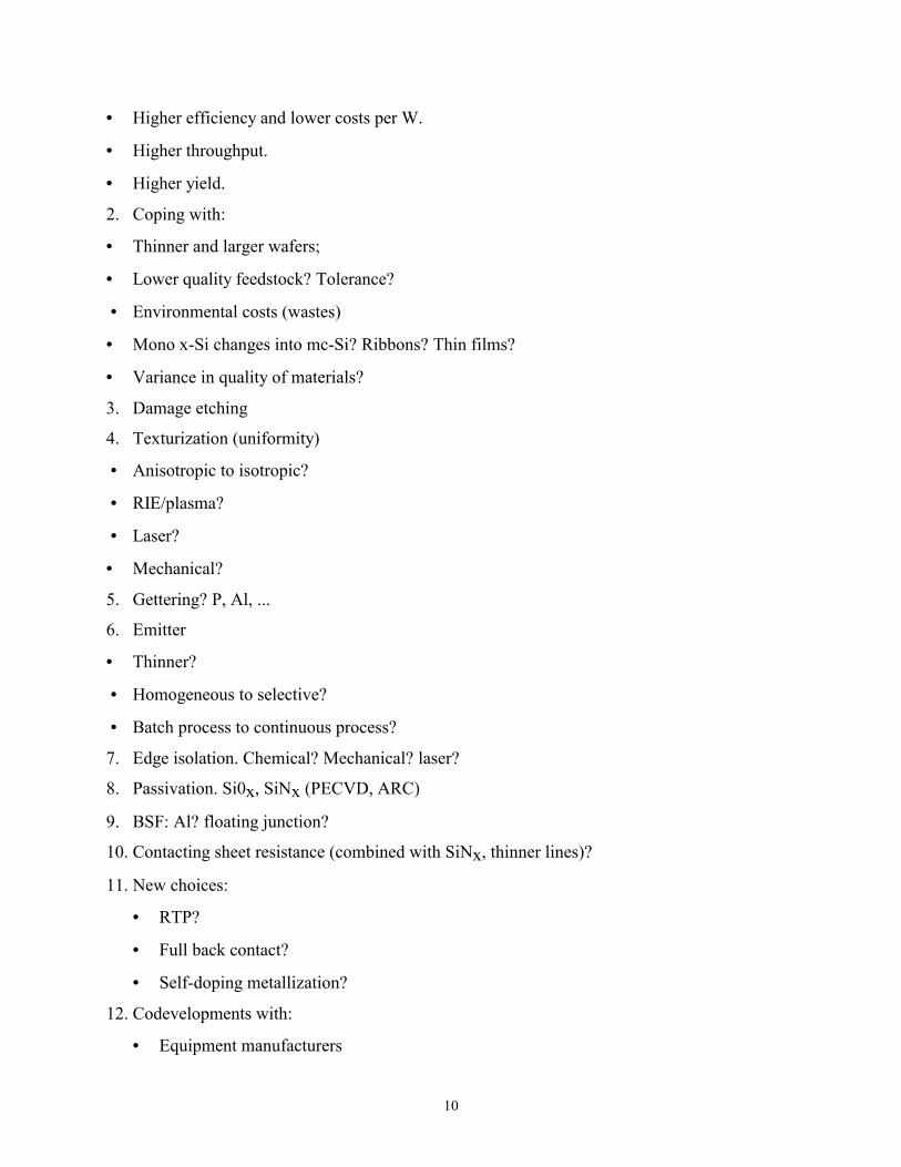
10
• Higher efficiency and lower costs per W.
• Higher throughput.
• Higher yield.
2. Coping with:
• Thinner and larger wafers;
• Lower quality feedstock? Tolerance?
• Environmental costs (wastes)
• Mono x-Si changes into mc-Si? Ribbons? Thin films?
• Variance in quality of materials?
3. Damage etching
4. Texturization (uniformity)
• Anisotropic to isotropic?
• RIE/plasma?
• Laser?
• Mechanical?
5. Gettering? P, Al, ...
6. Emitter
• Thinner?
• Homogeneous to selective?
• Batch process to continuous process?
7. Edge isolation. Chemical? Mechanical? laser?
8. Passivation. Si0x, SiNx (PECVD, ARC)
9. BSF: Al? floating junction?
10. Contacting sheet resistance (combined with SiNx, thinner lines)?
11. New choices:
• RTP?
• Full back contact?
• Self-doping metallization?
12. Codevelopments with:
• Equipment manufacturers
11
• Wafer manufacturers,
• Materials manufacturers.
Session 7. Process Monitoring
Chairpersons: James Gee, Sandia National Laboratories Andrés Cuevas, FEIT, Australian National University
Process monitoring may be separated into off-line monitoring and on-line process
monitoring/control. Off-line monitoring is for process development purposes, including gathering
of comprehensive data and detailed analysis, followed by problem solving and process
optimization. On-line process monitoring/control applies to all steps, from the incoming wafers
to finished cell products. On-line process monitoring/control serves two crucial functions: (i) to
provide feedbacks to correct the process step; and (ii) to provide a data-base for sorting out off-
spec wafers after each process step. These two functions should be applied to all of the following
process steps, each with a group of measurements/tests:
1. Ingots: lifetime, resistivity
2. Wafers (incoming and after etching/cleaning): thickness, resistivity, lifetime, reflectivity
3. Diffusion: dopant weight, sheet resistance, lifetime
4. AR coating: lifetime, reflectivity
5. Contact formation: shunt resistance, contact resistance, open-circuit voltage, etc.
6. Device tests.
Opinions were expressed on implementing process monitoring schemes, including: carrying them
out on every wafer; wafer sampling; adding special control-wafers (e.g., FZ wafers in mc-Si line
for contamination checking); and not bothering with them if the machines are controlled tightly.
From the discussion, it became clear that more process control is prevalent in industry than is
commonly assumed. Often, this process monitoring is done with simple, effective measurements
(wafer color, weight) as contrasted to the sophisticated instrumentation that is frequently
12
advocated. This discussion proved valuable in clarifying the trade-offs between sophistication
and practicality in process control and monitoring.
The discussion was closed with two open questions:
1. Do we have appropriate monitoring techniques and instruments?
2. Do they provide adequate, excessive, or insufficient information?
Session 8. International Research Programs
Chairpersons: Martin Green, University of New South Wales Ajeet Rohatgi, Georgia Tech University
This session emphasized the need for international collaboration in areas that are somewhat less
sensitive to proprietary issues. This could include fundamental research issues, development of
PV standards, and equipment. A recent success story is the international collaboration that
appears to have speeded up the discovery of the fundamental reason for light degradation of CZ
Si solar cells (B-O complex formation) and led to a solution (the use of MCZ wafers and Ga
doping).
Collaborations among various semiconductor companies (at the international level) have been
very fruitful. Such collaborations can benefit commercial solar cell manufacturers in converting
high-cost, laboratory processes for fabricating high-efficiency cells into commercial processes.
Perhaps international collaboration can be used in the first step is to identify the best process/tool
on a cost-performance basis. Programs that have a broad geographic scope are already in place
in Europe.
Session 9. Thin-Film Silicon
Chairpersons: Bob Birkmire, Institute of Energy ConversionHarry Atwater, California Institute of Technology
13
The driving force for thin-film/layer Si cells is its potential cost-performance competitiveness
with bulk Si cells. To this end, a thin-film Si solar cell must have the potential to yield a module
efficiency of 13%–14%, at a cost level of <$100/m2 or <$2.00/Wp. It should also have the
potential to reach large-scale production within 10 years.
There are many approaches to thin Si cells. Of these, µc-Si film, possibly using low-temperature
processing to accommodate the use of a low-cost substrate, is particularly enticing. Such a cell
should have a desired grain size that exceeds the base thickness of 10–60 µm. It is expected that
the carrier lifetime will be controlled by intragranular defects. Light-trapping at both surfaces
becomes an issue for such thin cells. It is not certain that there will be a low-cost, high-
temperature substrate. It is also not certain that a viable low temperature (T<600oC) process can
be developed under the required cell efficiency of ~14%.
Wrap UP: Dick Swanson, SunPower Corporation
The following conclusions and recommendations were voiced during the wrap-up session.
Overall, the workshop received high marks as being one of the best so far in the series.
Generally, the papers were of the highest caliber. The consensus was that the format for this year
with no panel sessions, but rather lengthened discussion periods, was superior to the old format.
Poster sessions continue to be a very useful approach and the mixture of university, government
and industry people was well balanced.
Session 2. Poly Feedstock and Silicon Growth
It was concluded that the feasibility for a non-Siemens, lower-cost process for generating solar
grade silicon has been convincingly demonstrated. The volume manufacturing cost is still
uncertain, but appears likely to meet DOE goals. Implementation of new capacity for solar grade
silicon awaits the emergence of sufficient demand and investment—either direct investment from
industry or large, guaranteed, fixed-price orders justifying the investment. At this time, a chronic
feedstock shortfall (using microelectronics industry scrap) is not expected until 2005 or later.
Sometime after that, it is expected that PV industry growth will create more demand than the
14
scrap supply availability, and it is hoped that dedicated solar-grade plants will then be
constructed to make up the shortfall. In the meantime, a modest research effort in solar-grade
silicon is warranted to help define required material characteristics and pave the way for solar-
grade silicon plants.
It was recommended that the workshop conduct periodic evaluations to ensure that feedstock
availability is meeting demand, that cost are decreasing, and that no shortage is looming. This
issue should play a minor role in the next workshop.
Session 3. Impurities and Defects in PV-Si
Dramatic advances in the understanding of Fe and Cu diffusion were presented. This sets the
stage for a better understanding of the diffusion of other transition metals. It would appear that
the necessary input parameters for the physics-based modeling of metal diffusion and gettering
are falling into place. Many results on precipitates were presented. A surprising result was that
Fe-O complexes may be more prevalent than Fe-Si precipitates. Fe-O precipitates are more
difficult to dissolve (and hence getter) than Fe-Si precipitates, and probably form when
interstitial oxygen is supersaturated (as it often is). Another somewhat surprising result is that
precipitation occurs mainly at inter-granular defects, rather than grain boundaries.
The issue of how, and even if, precipitates are passivated by hydrogen is still unresolved. It is
expected that certain types of precipitates will be more easily passivated than others. It would be
good to know which these are, and how to encourage easily passivated precipitates to form at the
expense of more detrimental precipitates. In fact, despite all the investigation of defects, it is still
generally not known what defect is the dominant lifetime killer in typical situations encountered
in different types of commercial cells. Along this line, the understanding of the comparative role
of intrinsic defects, transition metals, and complexes of these is still in its infancy. It is felt that,
while the role of oxygen has been extensively studied, and oxygen’s role in lifetime reduction is
somewhat understood, the expected similar impact of carbon and nitrogen has had little
investigation. This is perhaps because oxygen is very important in CZ material used in
microelectronic processing, and this material has comparatively less carbon and nitrogen. In
many types of solar silicon, this situation is reversed.
15
The session is a centerpiece of the workshop and should continue to play a major role in largely
its present form.
Session 4. Mechanical Properties
The session on mechanical properties proved to be very interesting and timely, as manufacturers
push wafer thickness down and breakage becomes more of an issue. While it is widely known
that stress near microcracks initiates breakage, the source of the microcracks has not been
extensively explored. One major source has proven to be ingot grinding, which results in
microcracks at the edge of the wafer. Removal by etching makes wafers twice as strong. Process
equipment changes can greatly reduce breakage. For example, replacing spin dryers with
alternatives that do not subject the wafers to mechanical stress has proven beneficial. Tri-crystals
have been shown to be stronger than single crystals, and may provide an avenue to thinner
wafers. In the end, however, wafer warpage caused by the thermal expansion mismatch of metal
layers on silicon provides a fairly basic limit to how thin wafers can be successfully processed.
In order to continue reducing wafer thickness (and hence material usage), it is necessary to
explore processes and equipment that do not stress or scratch wafers. For the next workshop, it is
recommended that sessions on low-stress processing and the origin of microcracks be organized.
Session 5: Passivation
The understanding of hydrogen in silicon continues to increase at a rapid rate. Some new, or
nearly new, results include consensus that the H-V complex is immobile, and thus cannot be a
source of H diffusion. It is electrically active, however. All dangling bonds must be passivated in
defects for the defect to be passivated. Thus, the V-H4 is passivated and not electrically active.
Atomic H is formed from the V-H2 interaction and can be a source of further passivation. Along
this line, silicide precipitates cannot be passivated. It is not known if oxide precipitates can be
passivated. Strained bonds are a possible point of attack of H, and this represents an opportunity
for H to do damage, making things worse. Thus, a very complex picture of H passivation is
emerging. There is no disagreement on the benefit of H passivation in improving cell
performance, however, especially on non-single crystal material. So far, silicon nitride has
16
proved the best source of H for passivation. Fortunately, it is possible to build high throughput
PECVD machines for depositing silicon nitride on a large scale.
More work is still needed to identify the actual defects that are being passivated in typical
industrial processes. While it is known that complete hydrogenation of dangling bonds is
necessary for passivation, it is not known if it is sufficient in all cases. We need to improve our
understanding of what needs to be passivated and better understand the comparative role of
dangling bonds and decorated defects. These topics should continue to play a major role in the
workshop.
Session 6. Solar Cell Processing
Much was learned about solar cell processing at this workshop. One of the more surprising
findings is that the observed optical degradation in a CZ solar cell is clearly caused by a B-O
complex rather than the B-Fe complex as originally postulated. Along this line, this degradation
can be avoided by simply switching from B to Ga as the base dopant. Proper process design
(aimed at preventing B-O complex formation) will also greatly reduce this degradation
mechanism. A much better understanding of the metal-precipitate dissolution process has
emerged with the controlling role of dissolved metal solubility having been elucidated. It was
demonstrated that the major improvement from Al BSF formation, in standard-thickness cells,
comes not from the BSF but from the concomitant gettering. Many selective emitter processes
have been demonstrated. A recent one is alloy-junction doping using doped contact metal, which
shows some promise. Insuring reliable contact wetting is the most serious issue in need of
resolution to make this scheme work. Other new approaches are made possible by a new
generation of screen printers that can do accurate inter-level alignments. It was pointed out that
so far, however, no selective emitter process has entered volume production (with the exception
of the LBC cell). A summary slide was presented showing the improvements that have been
introduced into production in the last 20 years. These included (1) screen printed contacts, (2)
belt diffusion, (3) surface passivation and hydrogenation, (4) wire saws, (5) back surface fields.
Many other candidates for improvements have not been introduced. The difficulty of introducing
new processes into existing production is often cited. Sometimes the issue comes from the
requirement for new equipment (and often profits do not justify new capital expenditure) and
17
sometimes the problem is that new, higher efficiency processes are simply not cost effective.
Nevertheless, there is a consensus that research on higher efficiency must continue because the
long-range economic viability of silicon solar cells is dependent on improvement in performance.
Most feel that some new self-aligned emitter processes will make it into production within the
next 3 years. Along another front, it has been demonstrated that most, if not all, the wet-
chemical process steps can be replaced with gaseous ones. This will reduce chemical
consumption and waste-disposal cost.
Major fronts for continued research on cell processing include developing a production-worthy
selective emitter and a cost-effective gettering procedure. Many gettering procedures require
long furnace cycles (difficult to integrate into a high-volume line) and expensive etching steps to
remove the getter region. Further exploration of RTP and gaseous processes may result in a
practical, low-cost gettering process. The needs of the solar cell industry have diverged greatly
from the microelectronic industry (which originally supplied most of the basic processing
concepts and methods) because of the very high wafer throughput needed in today’s large
manufacturing operations. These topics should continue to play a major role in future
workshops. Attendees felt that maintaining a good balance between basic defect science and cell
manufacturing is crucial to meeting the goals of the workshop.
Session 7. Process Monitoring
Further effort on high-throughput statistical process control is needed. The session on process
monitoring was interesting both for the new techniques introduced as well as for the perspective
of the industry participants. New techniques included a simple method to determine the effects
of trapping on PCD lifetime measurement and a new instrument to measure solar cell reflectance.
This instrument, called PV Reflectometer, can quickly measure a wide variety of solar cell
parameters, including, surprisingly, metal thickness. Industry participants emphasized the
requirement for very high uptime on all process monitoring equipment due to the high
throughput of current manufacturing facilities. The methodology of measuring most parameters
of interest now exists, and it remains to convert this into high-throughput and reliable production
machines. One desirable measurement that still has no good technique, however, is lifetime
measurements in cast polysilicon boules.
18
For the next generation of 100-MW/yr production facilities, the major scale up issues facing
manufacturers are high throughput process monitoring and control and automation. Further work
on these areas is important.
Session 8. Thin Film Silicon
There has been roughly a percentage point improvement in efficiency on deposited silicon cells
since the last workshop. Efficiencies in the 10% to 12% range have been achieved by several
techniques. Cells have been made in material with a wide range of grain size, spanning 10 nm to
1 mm. The region between 100 nm and 10 µm is very difficult. The details of substrate surface
morphology are very important in determining the grain size obtained during deposition. A
potentially important new development is a glass ceramic from Corning. This material allows
processing up to 950°C and has enabled deposited devices as good as those that can be obtained
on oxidized silicon wafers. In addition, several new approaches involving lift-off and transfer
processes are being investigated. These approaches result in single crystal layers and might yield
efficiencies as high as 17% with sufficient development.
This workshop should continue to explore the development of thin-film silicon cells. A
suggestion for future topics would be to invite industry representatives from the display
industries who are working on lift-off and transfer of III-V materials. This would encourage
cross-fertilization of ideas from the display and PV communities.
19
Program Committee
James Gee, Tadashi Saitoh, Michael Stavola, Dick Swanson, Juergen Werner, Teh Tan, Eicke
Weber, Ron Sinton, Juris Kalejs and Bhushan Sopori
Administrative Support
Sandy Padilla
AcknowledgementsA special note of appreciation goes to the following companies for their contributions to the
Graduate Student Award:
AstroPower, Crystal Systems, EBARA Solar, Evergreen Solar, Siemens Solar Industries, and
BP Solarex
REPORT DOCUMENTATION PAGE Form ApprovedOMB NO. 0704-0188
Public reporting burden for this collection of information is estimated to average 1 hour per response, including the time for reviewing instructions, searching existingdata sources, gathering and maintaining the data needed, and completing and reviewing the collection of information. Send comments regarding this burdenestimate or any other aspect of this collection of information, including suggestions for reducing this burden, to Washington Headquarters Services, Directorate forInformation Operations and Reports, 1215 Jefferson Davis Highway, Suite 1204, Arlington, VA 22202-4302, and to the Office of Management and Budget, PaperworkReduction Project (0704-0188), Washington, DC 20503.
1. AGENCY USE ONLY (Leave blank) 2. REPORT DATENovember 1999
3. REPORT TYPE AND DATES COVEREDConference Proceedings
4. TITLE AND SUBTITLENinth Workshop on Crystalline Silicon Solar Cell Materials and Processes: Summary DiscussionSessions, 9-11 August 1999, Breckenridge, Colorado6. AUTHOR(S)B. Sopori, T. Tan, D. Swanson, M. Rosenblum, and R. Sinton
5. FUNDING NUMBERS
C: TA: PV002501
7. PERFORMING ORGANIZATION NAME(S) AND ADDRESS(ES) 8. PERFORMING ORGANIZATIONREPORT NUMBER
9. SPONSORING/MONITORING AGENCY NAME(S) AND ADDRESS(ES)National Renewable Energy Laboratory1617 Cole Blvd.Golden, CO 80401-3393
10. SPONSORING/MONITORINGAGENCY REPORT NUMBER
CP-520-275711. SUPPLEMENTARY NOTES
12a. DISTRIBUTION/AVAILABILITY STATEMENTNational Technical Information ServiceU.S. Department of Commerce5285 Port Royal RoadSpringfield, VA 22161
12b. DISTRIBUTION CODE
13. ABSTRACT (Maximum 200 words)This report is a summary of the panel discussions included with the Ninth Workshop on Crystalline Silicon Solar Cell Materials andProcesses. The theme for the workshop was “R&D Challenges and Opportunities in Si Photovoltaics.” This theme was chosen because itappropriately reflects a host of challenges that the growing production of Si photovoltaics will be facing in the new millennium. Theanticipated challenges will arise in developing strategies for cost reduction, increased production, higher throughput per manufacturingline, new sources of low-cost Si, and the introduction of new manufacturing processes for cell production. At the same time, technologiesbased on CdTe and CIS will come on line posing new competition. With these challenges come new opportunities for Si PV to wean itselffrom the microelectronics industry, to embark on a more aggressive program in thin-film Si solar cells, and to try new approaches toprocess monitoring.
15. NUMBER OF PAGES 14. SUBJECT TERMSphotovoltaics ; crystalline silicon ; solar cells ; materials and processes; feedstocks ; impuritiesand defects ; passivation 16. PRICE CODE
17. SECURITY CLASSIFICATIONOF REPORTUnclassified
18. SECURITYCLASSIFICATIONOF THIS PAGEUnclassified
19. SECURITY CLASSIFICATIONOF ABSTRACTUnclassified
20. LIMITATION OF ABSTRACT
UL
NSN 7540-01-280-5500 Standard Form 298 (Rev. 2-89)Prescribed by ANSI Std. Z39-18
298-102