Embed Size (px)
Citation preview
Next Generation Wireless Receiver Architecture Design inDeep-Sub-Micron CMOS Technology
Chaoying Wu
Electrical Engineering and Computer SciencesUniversity of California at Berkeley
Technical Report No. UCB/EECS-2016-181http://www2.eecs.berkeley.edu/Pubs/TechRpts/2016/EECS-2016-181.html
December 1, 2016

Copyright © 2016, by the author(s).All rights reserved.
Permission to make digital or hard copies of all or part of this work forpersonal or classroom use is granted without fee provided that copies arenot made or distributed for profit or commercial advantage and that copiesbear this notice and the full citation on the first page. To copy otherwise, torepublish, to post on servers or to redistribute to lists, requires priorspecific permission.

Copyright @ 2014
by
Chaoying Wu

The Dissertation Committee for Chaoying (Charles) Wu Certifies that this is the
approved version of the following dissertation:
Next Generation Wireless Receiver Architecture Design in
Deep-Sub-Micron CMOS Technology
Committee:
Prof. Borivoje Nikolic, Chair
Prof. Ali M. Niknejad
Prof. David J. Allstot
Prof. Paul K. Wright
Next Generation Wireless Receiver Architecture Design in
Deep-Sub-Micron CMOS Technology
by
Chaoying (Charles) Wu
A dissertation submitted in partial satisfaction of the
requirements for the degree of
Doctor of Philosophy
in
Engineering – Electrical Engineering and Computer Sciences
in the
Graduate Division
of the
University of California, Berkeley
Committee in charge:
Professor Borivoje Nikolic, Chair
Professor Ali M. Niknejad
Professor David J. Allstot
Professor Paul K. Wright
May, 2014

Day before yesterday I saw a rabbit, and yesterday a deer, and today, you.
--- The Dandelion Girl, Robert F. Young
To my parents, Uncle Shaw and Sherri.
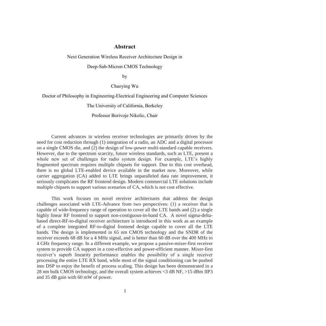
Abstract
Next Generation Wireless Receiver Architecture Design in
Deep-Sub-Micron CMOS Technology
by
Chaoying Wu
Doctor of Philosophy in Engineering-Electrical Engineering and Computer Sciences
The University of California, Berkeley
Professor Borivoje Nikolic, Chair
Current advances in wireless receiver technologies are primarily driven by the
need for cost reduction through (1) integration of a radio, an ADC and a digital processor
on a single CMOS die, and (2) the design of low-power multi-standard capable receivers.
However, due to the spectrum scarcity, future wireless standards, such as LTE, present a
whole new set of challenges for radio system design. For example, LTE’s highly
fragmented spectrum requires multiple chipsets for support. Due to this cost overhead,
there is no global LTE-enabled device available in the market now. Moreover, while
carrier aggregation (CA) added to LTE brings unparalleled data rate improvement, it
seriously complicates the RF frontend design. Modern commercial LTE solutions include
multiple chipsets to support various scenarios of CA, which is not cost effective.
This work focuses on novel receiver architectures that address the design
challenges associated with LTE-Advance from two perspectives: (1) a receiver that is
capable of wide-frequency range of operation to cover all the LTE bands and (2) a single
highly linear RF frontend to support non-contiguous-in-band CA. A novel sigma-delta-
based direct-RF-to-digital receiver architecture is introduced in this work as an example
of a complete integrated RF-to-digital frontend design capable to cover all the LTE
bands. The design is implemented in 65 nm CMOS technology and the SNDR of the
receiver exceeds 68 dB for a 4 MHz signal, and is better than 60 dB over the 400 MHz to
4 GHz frequency range. In a different example, we propose a passive-mixer-first receiver
system to provide CA support in a cost-effective and power-efficient manner. Mixer-first
receiver’s superb linearity performance enables the possibility of a single receiver
processing the entire LTE RX band, while most of the signal conditioning can be pushed
into DSP to enjoy the benefit of process scaling. This design has been demonstrated in a
28 nm bulk CMOS technology, and the overall system achieves <3 dB NF, >15 dBm IIP3
and 35 dB gain with 60 mW of power.
1
vi
Acknowledgements
I have had the honor to work and interact with a group of very intelligent and
talented individuals at Berkeley. Without them, my stay in Berkeley would not be as
memorable.
First and upmost, I can take this opportunity to express my gratitude to my
advisor, Professor Bora Nikolic, for his vision and his dedication to research.
I would like to thank members of my project group, Professor Ali Niknejad for
the most insightful discussions, Professor David Allstot for constant encouragement,
Professor Elad Alon for always upholding the highest standards.
I have had many lengthy discussions with Christopher Hull and Ken Nishimura
during my internships as well as formative stages of my research. My internship
experience with Intel and Agilent enriched my knowledge, and widened my view in
many perspective. I thank Haideh Khorramabadi, Tom Kwan and David Sobel for many
constructive suggestions on research and career. Also, I thank Michael Reiha for his
countless effort on teaching me how to properly write a scientific paper. I also appreciate
all the helps from Professor Jason Stauth and Professor Seth Sanders.
I was based in BWRC for the most part of my Ph.D. career. I consider it a
privilege to be associated with the center. The resource and level of collaboration is
unmatched. Senior students and staff laid the foundation that made my research possible.
I learned how to use the HFSS emulation platform from Lingkai Kong. I appreciate his
effort in listening to me and providing the best solutions. I thank Brian Richards for his
supports with my chip design. I was also lucky to have a period of overlap with Jiashu
Chen and Jun-Chau Chien, who shared their great depth of design experience. Many
thanks go to Yue Lu for always being patient with my questions and helps in emulation
and design. Special thanks go to Gary Kelson, Tom Boot, Kevin Zimmerman and other
staff members for making BWRC such a pleasant place to work.
The friendship of many peers in Berkeley is perhaps one of the best memories that
I will take with me of my graduate studies. I have very much enjoyed being part of
DCDG/Bora’s group. Zheng Guo, Seng-Oon Toh, Ji-Hoon Park, Dusan Stepanovic,
Vinayak Nagpal, Milos Jorgovanovic, Matt Weiner, Sharon Xiao, Katerina
Papadopoulou, Jawhwa Kwak and Brian Zimmer have made my stay very memorable.
For outside of the group, I appreciate Amin Arbabian’s perspective in life, career and in
research and most importantly I am thankful for his friendship throughout the years. I
thank Siva Thyagarajan for being a loyal friend and for giving me many constructive and
critical feedback and support on my research; I have benefited much from our

vii
discussions. I also thank Steven Callender and Shinwon Kang for discussions regarding
our common research interests.
Finally, my gratitude goes to my family, who has been a perpetual source of
comfort and encouragement. They taught me the values of life, the importance of
integrity and work ethics, which I only learn to appreciate gradually over time. They
always valued my honest effort, no matter how minuscule. They provided the best
cushion to allow me to recover from each setback and become more determined. I
dedicate this work to them for their love and support that made it possible.
viii
Table of Contents
List of Tables ...................................................................................................... xi
List of Figures ...................................................................................................... xii
Chapter 1 Introduction ......................................................................................1
1.1 Related Work ............................................................................................6
1.2 Thesis Organization ..................................................................................8
Chapter 2 Software-Defined Radio Receiver Design .....................................11
2.1 RF Receiver Design Principles ...............................................................11
2.2 RF Convertor Receiver Design ...............................................................14
2.2.1 Overview on ΔΣ ADC Design ....................................................15
2.2.2 ΔΣ ADC in RF Receivers ...........................................................19
2.3 Digital-Assist Receiver Architecture ......................................................20
2.3.1 Passive Mixer-First Receiver Design..........................................20
2.4 Understanding the Wireless Standards ...................................................21
2.5 Performance Comparison of Exisiting Designs ......................................31
2.5.1 Software-Defined Radio Implemenation ....................................35
Chapter 3 ΔΣ Receiver System Architecture .................................................36
3.1 Introduction .............................................................................................36
3.2 Receiver Architecture .............................................................................37
3.2.1 System Level Design ..................................................................37
3.2.2 Loop Filter Structure ...................................................................40
3.2.3 Jitter Sensitivity ..........................................................................46
3.2.4 Current-Mode-Integration Mixing/Sampling..............................52
3.3 Summary .................................................................................................59
Appendix A Derivation of Multi-Bit RZ and NRZ DAC Jitter Sensitivity ..60
Chapter 4 ΔΣ Receiver Experimental Prototype ...........................................63
4.1 Introduction to System Implementation..................................................63
ix
4.2 Circuit Design Details .............................................................................65
4.2.1 Sub-Channel Design ...................................................................65
4.2.2 Low Noise Transconductance Amplifier ....................................67
4.2.3 Feedback DAC Designs ..............................................................74
4.2.4 Comparator Design .....................................................................77
4.2.5 LO Generation and Distribution .................................................80
4.3 Measurement Results ..............................................................................82
4.4 Conclusion ..............................................................................................91
Chapter 5 Mixer-First Receiver Design Considerations ...............................92
5.1 Introduction to Passive CMOS Mixer.....................................................92
5.2 Passive-Mixer First Receiver Design......................................................93
5.3 Baseband Trans-Impedance Amplifier (BB-TIA) Design ......................97
5.3.1 Noise Analysis for BB-TIA ........................................................99
5.3.2 Analysis for BB-TIA Out-of-Band Linearity ...........................102
5.4 Harmonic Rejection System .................................................................105
5.4.1 Harmonic Folding and Noise Figure Performance ...................105
5.4.1 Harmonic Rejection System Design .........................................107
Appendix B Mixer Linearity Analysis ........................................................116
Chapter 6 Circuit Prototype for a Mixer-First Receiver Design ................125
6.1 Introduction ...........................................................................................125
6.2 System Overview ..................................................................................125
6.3 Circuit Design Details ...........................................................................127
6.4 Optimizing Noise Figure Performance .................................................133
6.5 Measurement Results ............................................................................136
6.6 Summary ...............................................................................................152
Chapter 7 Conclusion .....................................................................................153
7.1 Significant Contribution........................................................................154
7.2 Future Work ..........................................................................................155

x
Bibliography .......................................................................................................158
xi
List of Tables
Table 2.1: RF receiver performance summary ..............................................32
Table 2.2: A summary for modern multi-mode multi-radio designs ............34
Table 3.1: Comparision of Py Pyd on different levels of DACs .....................46
Table 3.2: SNR comprision between RZ and NRZ DACs with different DAC
levels ...........................................................................................47
Table 4.1: Parasitic capacitor extraction result for different capcaitor layout
topology ....................................................................................68
Table 4.2: Performance comparison table .....................................................87
Table 5.1: Gain allocation and Gm requirement for different value of RFB. ..98
Table 5.2: Filtering Versus out-of-band IIP3 ..............................................100
Table 6.1 Noise power breakdowns for noise integrated over different
bandwidth ..................................................................................120
Table 6.2 Comparison table with other state-of-art receiver designs .........137
Table 6.3 Comparison table with designs for LTE ....................................138
xii
List of Figures
Fig 1.1: Spectrum allocation for United States ...................................................2
Fig 1.2: The UK frequency allocations .............................................................3
Fig 1.3: Hong Kong frequency allocation chart .................................................4
Fig 1.4: Australian frequency allocation chart ....................................................4
Fig 2.1: The scenario of the near-far problem ..................................................11
Fig 2.2.a: A blocking mask for GSM ..................................................................12
Fig 2.2.b: A blocking mask for UMTS ................................................................12
Fig 2.3: Recent evolution of the RF receiver design ........................................14
Fig 2.4: A simple ΔΣ modulator .......................................................................16
Fig 2.5: Signal and noise transfer function of a second-order modulator .........16
Fig 2.6: Evolution of the wireless communication in the past thirty years ......23
Fig 2.7: Non-overlapping LO waveforms.........................................................18
Fig 2.8: LTE spectrum allocation across the world ..........................................24
Fig 2.9: Supporting LTE together with other wireless standards .....................24
Fig 2.10: Five different models of IPhone 5 for global support .........................25
Fig 2.11: Five sub-carrier carrier aggregation to generate a higher bandwidth ..26
Fig 2.12: LTE carrier aggregation between the licensed and unlicensed bands .27
Fig 2.13: System requirement for a device supporting LTE CA ........................27
Fig 2.14: Samples of the supported channels from a commercial design ...........28
Fig 2.15: Three different scenarios for carrier aggregations ..............................29
Fig 2.16: Channel bonding for two 20 MHz channels ........................................30
Fig 3.1: Band-pass ΔΣ modulator loop filter in Z transform ............................38
Fig 3.2: Band-pass feedback created with two SD Modulator .........................39
Fig 3.3: A second order CIFB ΔΣ loop filter ....................................................40
Fig 3.4: Signal and noise transfer functions of a second order modulator .......41
Fig 3.5: Simulation results with complex zeroes ..............................................41
Fig 3.6: A simplified ΔΣ loop filter ..................................................................42
Fig 3.7: Signal transfer function peaking in CIFF architecture ........................44
Fig 3.8: A simplified ΔΣ loop model for FIR DAC .........................................45
Fig 3.9: A simplified ΔΣ loop model with phase noise ....................................46
xiii
Fig 3.10: Simulated output spectrum with phase noise model ...........................47
Fig 3.11: Time domain output waveform for ΔΣ ADCs with different quantizer
levels .................................................................................................48
Fig 3.12: Comparison of jitter impact on RZ and NRZ DACs ...........................50
Fig 3.13: Equivalent sampling model in time domain ........................................53
Fig 3.14: Equivalent sampling model in frequency domain ...............................53
Fig 3.15: Effect of frequency domain of using sampling to downconvert RF signal
..........................................................................................................54
Fig 3.16: Equivalent mixing model in time domain ...........................................55
Fig 3.17: Equivalent mixing model in frequency domain ..................................55
Fig 3.18: Effect of frequency domain of using mixing to downconvert RF signal
..........................................................................................................56
Fig 3.19: Current-mode integration sampler with single-ended output ..............57
Fig 3.20: Equivalent model for CMIS to downconvert RF signal in frequency
domain ..............................................................................................58
Fig 4.1: Simplified block diagram of the entire receiver ..................................63
Fig 4.2: Simplified schematic of the I-channel .................................................65
Fig 4.3: Low noise trans-conductance front-end design with bias ...................67
Fig 4.4: Transformer-based output combining network ...................................68
Fig 4.5: Noise simulation result of LNTA under different blocker level .........69
Fig 4.6: LNTA linearity simulation results .......................................................70
Fig 4.7: Graphical explanation of the LNTA under large blocker transient .....70
Fig 4.8: Detail schematic and clocking scheme for FB-DAC1 ........................72
Fig 4.9: System model including the effects of feedback DAC finite output
resistance ...........................................................................................73
Fig 4.10: Schematic for the quantizer design .....................................................75
Fig 4.11: Quantizer area comparison with and without calibration ....................76
Fig 4.12: Quantizer area breakdown with calibration .........................................76
Fig 4.13: Quantizer power comparison with and without calibration ................77
Fig 4.14: LO generation and distribution network .............................................78
Fig 4.15: Chip microphotograph .........................................................................79
Fig 4.16: Measurement setup for data capturing and system control .................80
Fig 4.17: Measured SNR at 2 GHz carrier frequency.........................................81
xiv
Fig 4.18: Measured SNR and SNDR at 2 GHz carrier frequency ......................82
Fig 4.19: Output spectrum at 2 GHz center frequency with input signal offset by
1MHz ................................................................................................82
Fig 4.20: Flicker noise from LO chain upconversion and downconversion .......83
Fig 4.21: Two tone tests with 1 MHz tone spacing around 2 GHz center frequency
..........................................................................................................83
Fig 4.22: IIP3 versus two-tone spacing at 2 GHz ...............................................84
Fig 4.23: SNR, SNDR vs. Signal Bandwidth .....................................................84
Fig 4.24: SNDR versus carrier frequency ...........................................................85
Fig 4.25: Power breakdown for the entire receiver system ..............................86
Fig 5.1: Simplified circuit model of passive mixer ..........................................91
Fig 5.2: Non-overlapping LO waveforms.........................................................91
Fig 5.3: Passive Mixer-first receiver with baseband TIA .................................93
Fig 5.4: Equivalent noise model for mixer-first design ....................................93
Fig 5.5: Different amplifier structure candidates for BB-TIA design ..............94
Fig 5.6: Noise figure (NF) for OTA and Op-amp with different feedback Resistors
..........................................................................................................96
Fig 5.7: Noise figure with the second stage amplification stage ......................97
Fig 5.8: BB-TIA with CL and CFB ................................................................101
Fig 5.9: Input Impedance with CL and CFB. .................................................101
Fig 5.10: Harmonic noise folding .....................................................................103
Fig 5.11: The idea of harmonic rejection ..........................................................104
Fig 5.12: System level implementation of harmonic rejection .........................104
Fig 5.13: Oversampling and time domain interleaving sampling .....................105
Fig 5.14: Time-domain interleaving sampling with different duty cycle .........105
Fig 5.15: Aliasing content within one slower sampling path ...........................106
Fig 5.16: Aliasing contents in each of the paths ...............................................106
Fig 5.17: Imperfect alignment due to the presence of mismatch ......................108
Fig 5.18: Incomplete harmonic cancelation due phase and gain mismatch ......109
Fig 5.19: Performance limitation due to mismatches .......................................109
Fig 5.20: Behavior model for time-interleave system with phase and gain
mismatches......................................................................................109
Fig 5.21: Gain and phase mismatches degrade the HR performance ............110
xv
Fig 5.22: Phase mismatches simulation .............................................................. 111
Fig 5.23: HR ratio measured with 50%, 25% and 12.5% duty cycle LO ............. 111
Fig 5.24: LO with different duty cycle for harmonic rejection............................. 112
Fig 6.1: Top-level system overview for mixer-first design ................................ 114
Fig 6.2: Schematic for the mixer core and unit cell in the mixer DAC. ............. 114
Fig 6.3: Layout for the differential mixer cells ................................................... 115
Fig 6.4: Inverter-based amplifier design with CMFB and its bias scheme ......... 116
Fig 6.5: Instability of a two-stage amplifier design. ........................................... 117
Fig 6.6: AC-boosting compensation (ACBC) scheme ........................................ 118
Fig 6.7: Detail schematic design for second stage amplifier design ................... 118
Fig 6.8: Floor planning for the entire system ...................................................... 119
Fig 6.9: Noise power breakdown during large signal transient .......................... 121
Fig 6.10: Mixer noise power break down. ............................................................ 122
Fig 6.11: Chip Microphotograph .......................................................................... 123
Fig 6.12: LO leakage before calibration. .............................................................. 124
Fig 6.13: LO leakage after calibration. ................................................................. 125
Fig 6.14: S11 over wide range of frequencies ...................................................... 126
Fig 6.15: Measured noise figure performance from 250 MHz to 3.5 GHz .......... 127
Fig 6.16: Measured NF performance with different baseband bandwidth ........... 129
Fig 6.17: Noise figure measurement result with various blocker power level ..... 130
Fig 6.18: Test setup for measuring far-out IIP3 .................................................... 131
Fig 6.19: Test setup for measuring close-in IIP3 .................................................. 132
Fig 6.20: In-band and out-of-band IIP3 measured ................................................ 133
Fig 6.21: Measured P1dB for in-band and out-of-band ........................................ 134
Fig 6.22: Measured in-band P1dB ........................................................................ 135
Fig 6.23: Power break down for major circuit blocks .......................................... 136
Fig 7.1: Sigma delta receiver with interference cancellation .............................. 141

xvi
1
Chapter 1
Introduction
Wireless connectivity has shown its immense significance in the past decade. The
continued technology scaling behind the very large system integration (VLSI) has
enabled multi-radio system design for mobile applications, which has not been possible
in the past century. This highly integrated system on chip (SoC) solution not only allows
mobile devices to achieve smaller form factors, but also make the latest wireless
technologies more affordable and accessible than they ever were in the past. Coupled
with the unending desire for a faster data connection, the wireless connectivity continues
to grow, as new wireless standards are introduced to address different needs every year.
By now, a wide range of wireless standards exist. Each is highly optimized for power and
cost for its own applications, and hence they support different in data rate requirement
and cover different range.
It is challenging to support such a multitude of wireless standards with each of
them being so drastically different from another. To add to the matter, different countries
around the world allocate their spectrum in different ways, and even in the same country,
different service providers are operating at different frequency bands. A high-end cellular
handset device can support up to a dozen handful of different wireless standards such as
GSM, CDMA, UMTS, HSPA, WiFi, Bluetooth as well as LTE, and it is able to operate
over more than ten different frequency bands[1]. Up till now, transceiver ICs are often
designed with a particular wireless standard in mind, due to the huge difference in system
requirement between different standards. To achieve the desired support of the multitude
of wireless standards support, multiple chipsets are often required. Given the apparent
increase in the design complexity for wireless handset devices and the cost reduction
possibility offered by the continuous scaling of the modern CMOS technology, the
demand for a single uniform transceiver system which is capable for multi-standard and
multi-band operation is highly desired, but not yet available.
Moreover, spectrum scarcity is an increasingly important issue for the decade, and
therefore a flexible and dynamic spectrum allocation is preferable. Due to the
proliferation of the wireless standards in the past decade, a majority of the commercial
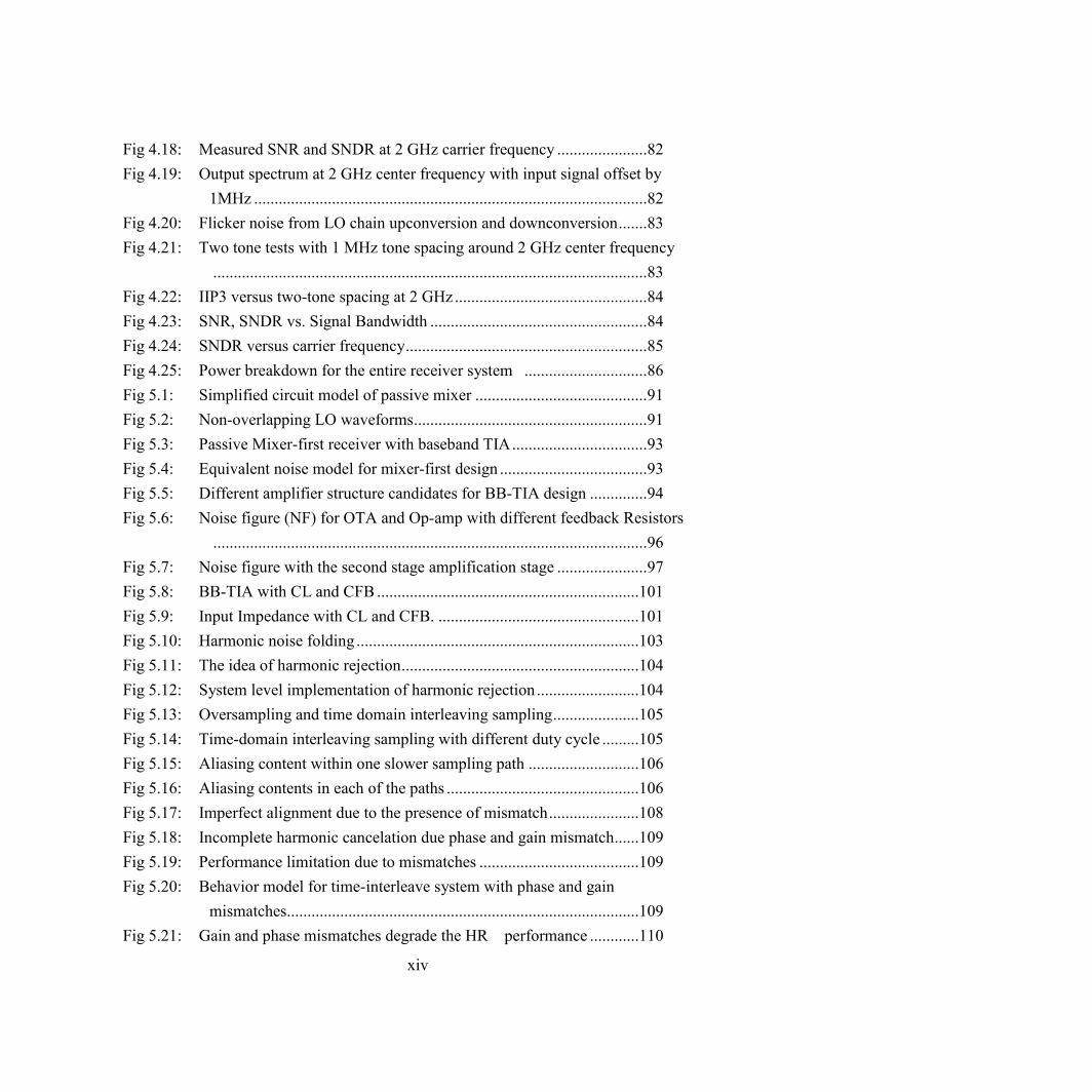
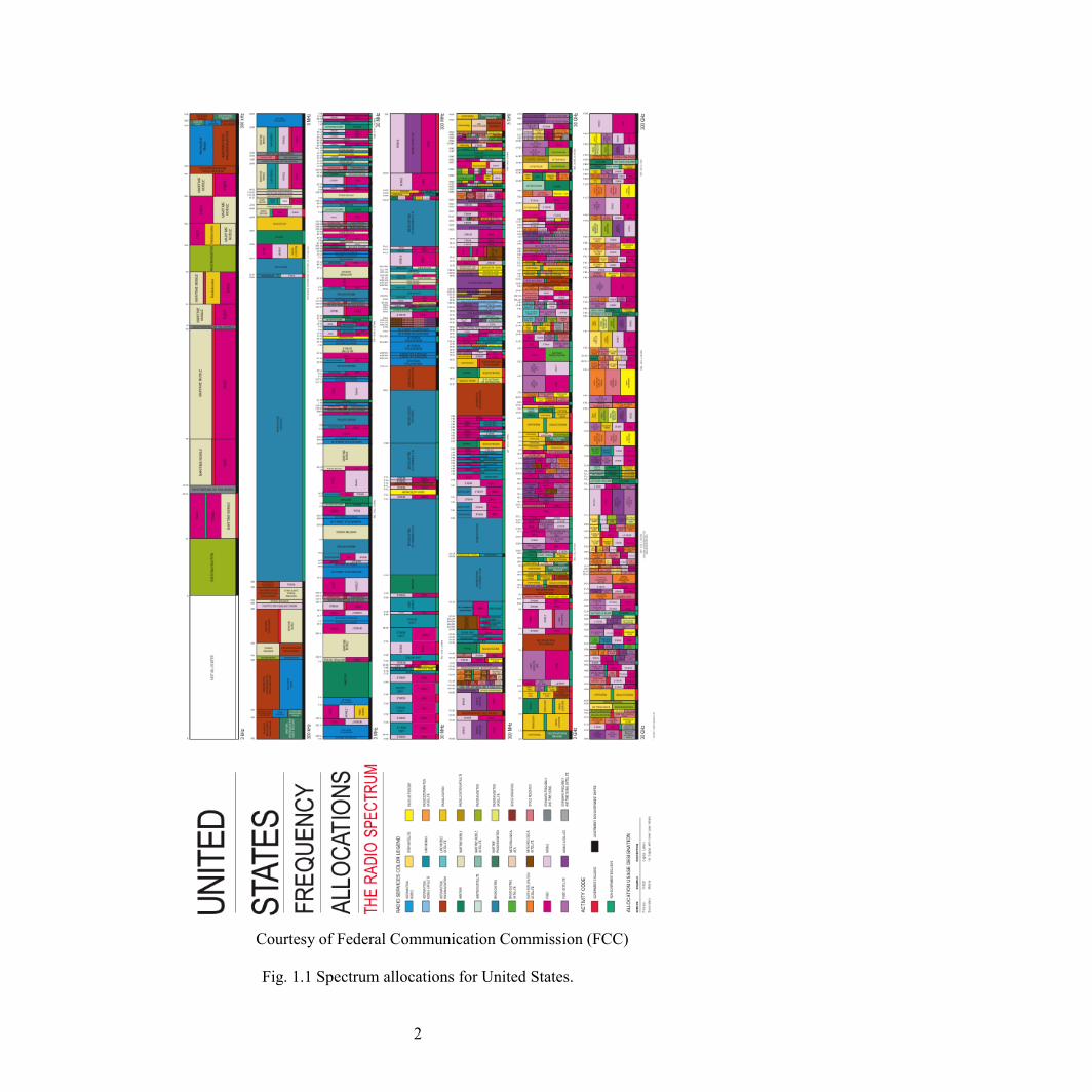
bands have been allocated to different standards (Fig. 1.1). As a result, the remaining
available frequency bands that can be allocated for future standards are quite limited,
while future wireless standards are still striving for a faster data rate and wider
bandwidth.
2
Courtesy of Federal Communication Commission (FCC)
Fig. 1.1 Spectrum allocations for United States.
3
The story of government spectrum licenses dated back to the 1920s [115], when
US official regulators realized that new transmitters might interfere with other system
operating in the radio spectrum. The result is that every wireless system required an
exclusive license issued by the government to operate; their operations in the radio
spectrum are closely monitored and governed by U.S. Federal Communication
Commission (FCC). After the introduction of the Advanced Mobile Phone System
(AMPS) in 1983 in Chicago, which marked the beginning of the personal wireless
application for civilians, it has been a thirty years of prosperity for the commercial
wireless communication. However, with virtually all usable radio frequencies issued to
different commercial operators and government branches, the inventory of wireless
spectrum is running low on the remaining available bands. The irony is that even though
wireless spectrum is something we cannot touch, smell, or see, it indeed is becoming one
of the most valuable nature resources known to the human kind.
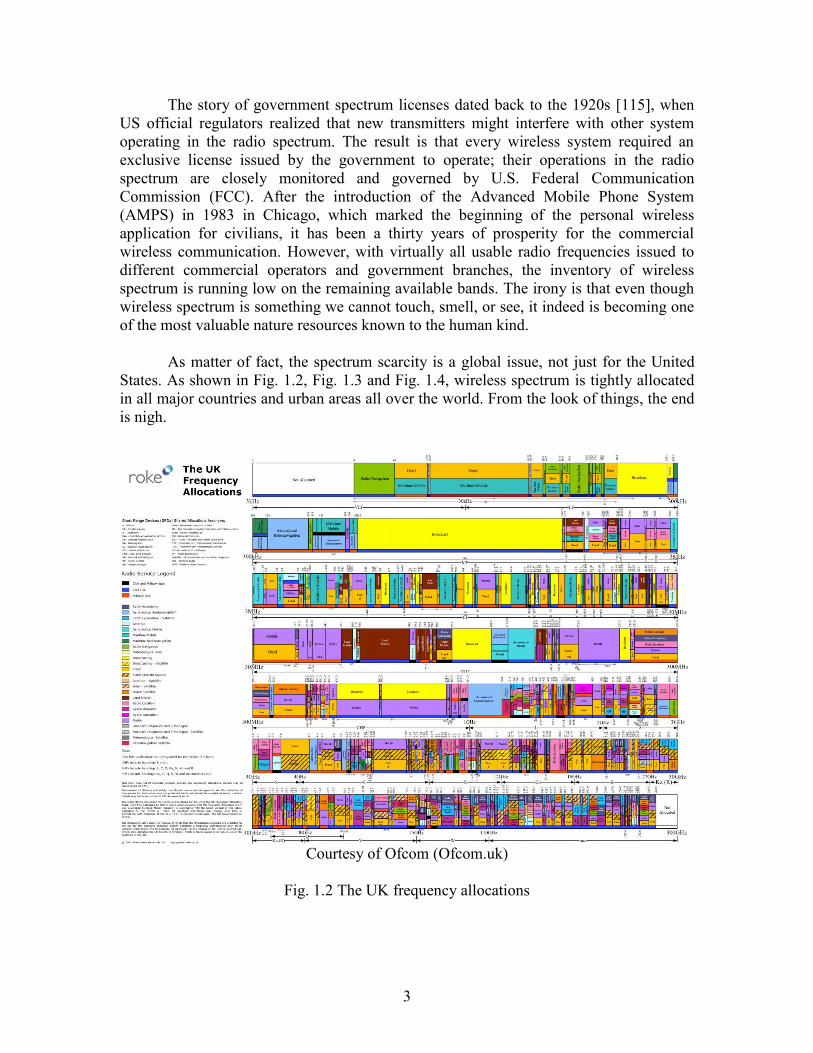
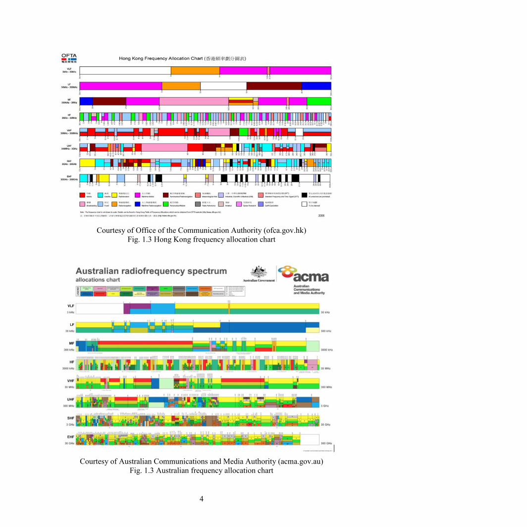
As matter of fact, the spectrum scarcity is a global issue, not just for the United
States. As shown in Fig. 1.2, Fig. 1.3 and Fig. 1.4, wireless spectrum is tightly allocated
in all major countries and urban areas all over the world. From the look of things, the end
is nigh.
Courtesy of Ofcom (Ofcom.uk)
Fig. 1.2 The UK frequency allocations
4
Courtesy of Office of the Communication Authority (ofca.gov.hk)
Fig. 1.3 Hong Kong frequency allocation chart
Courtesy of Australian Communications and Media Authority (acma.gov.au)
Fig. 1.3 Australian frequency allocation chart
5
Cognitive radio (CR) is one technology under research that could potentially
allow a more efficient use of the existing spectrum. While spectrum is auctioned off at
high price, researchers have noticed that most of the licensed frequency bands are being
under-utilized for most of the time [2], which suggest there is a potential to improve
efficiency of the spectrum usage by sharing it among other systems. The advantage of
cognitive radio is its feature of dynamic spectrum access (DSA), which allows different
system to look for the unused channels and time-share it.
Regulatory efforts from governments around the world also aim to solve the issue.
Cognitive radio is expected to operate in a large portion of the commercial spectrum in
the future. As for now, vacant channels have been or plan to be released by governments
for different applications. The new devices, known as TV band devices (TVBD) would
operate in those frequency bands. Japan, Singapore, the United Kingdom as well the as
the United States have been working on to support devices like this. For instance, the
European Conference of Postal and Telecommunications Administrations have opened
up the 470 to 790 MHz band for TVBD use.
In U.S, the FCC has established the fixed and the portable devices categories for
TVBDs. Fixed devices can transmit with a power up to 1 watt, and they may use any of
the vacant U.S. TV bands as 2, 5 to 36, and 38 to 51. On the other hand, the portable
devices shall operate in TV channels from 21 to 36 and from 38 to 51. The permitted
output is 100 mW EIRP, or at a reduced power level of 40 mW when there is an adjacent
TV channel.
While research and regulatory efforts aim to solve the issue of the spectrum
scarcity, the envisioned implementation of the CR poses a series of serious challenges on
the RF transmitter and receiver design. The RF transceiver system needs to be flexible
enough to adapt to different frequency band and different standards upon request, which
is a huge deviation from the conventional wireless design methodology, where RF
transceiver design is highly optimized by one set of application. On the other hand, a
faster and more affordable network is always desired, which puts a lot of pressure on the
future wireless standard in the absence of the CR. Before CR can be widely deployed, all
the future standards would have to struggle between the limited remaining spectrum and
the desire for higher data rate.
Long-Term Evolution (LTE) is the latest radio platform technology introduced to
the family of the commercial wireless systems. As the result of the increasing global
spectrum scarcity, LTE standard is a compromise that consists of total 43 separate bands
ranging from 450 MHz all the way up to 3.8GHz. All 43 bands of LTE are separated to
fit in the narrow available channels in different geographical regions, and the end result is
a highly fragmented spectrum over a wide frequency range, which makes LTE the most
difficult standard to provide world-wide support.
Another issue associated with the future wireless system is how to provide a
higher throughput with limited bandwidth available. A similar idea as CR has been
introduced to the latest wireless technologies, which is known as in-channel spectrum re-
6
allocation. The recent wireless standards, such as 802.11.ac and LTE all adopted similar
schemes. LTE Advanced introduces the idea of carrier aggregation, where multiple in-
channel sub-carriers can be allocated for the same user or different users in a wide range
of manners, while the 802.11.ac (5G WiFi) includes the idea of channel binding, where
the channel bandwidth allocated to a user can be expanded to achieve a much faster data
rate when it is possible.
A reconfigurable transceiver is desired because of its ease to cover wide range of
wireless standards and frequency bands, in particular it can be a cost-effective solution to
support the LTE fragmented spectrum. Moreover, it can be extended to support future
dynamic spectrum allocation, such as required by the cognitive radio. The final goal is a
single uniform transceiver system, which is sufficiently flexible to support the existing as
well as the future standards over a wide-range of frequency bands. The system would
ease on the difficulties to support multitude of existing standards as well as open up a
path for flexible spectrum allocation scheme for demanded to address the spectrum
scarcity issue.
1.1 Related Work
The idea of software-define radio (SDR) is first proposed by Joseph Mitola in
1992 [3]. A software-defined radio is a radio system such that most of its components are
implemented by means of software on a general purpose computing device or embedded
system. The ideal concept envisions a system which can monitor and transmit over the
entire RF spectrum. Since then, there are a few notable examples known as the
reconfigurable, or software-defined, RF receivers (SDR) such as references [4][5]
[6][7][17][27][30]. All the listed designs adapted the convectional chain of elements
design, where the systems begin with an RF amplification stage (LNA), followed by a
frequency conversion state (mixer). Then the down-converted signal is filtered by a high-
order low-pass filter prior to it reaches the ADC.
Throughout the years, there are a wide range of system implementation proposed
to fulfill the grand vision of SDR. In particular, one thing that stands out in the UCLA
design [5] is that it contains a low-power discrete-time low-pass filter. This filter makes
use of an old and yet well-known concept: the passive switched-capacitor filter, which is
popular choice for the baseband filter in RF receiver designs such as [5][7][8] and [9].
The passive switched-capacitor technique has several advantages, such as its precision in
the filter cut-off frequency, relaxed requirement on the amplifier settling time as opposed
to an active switched-capacitor filter design.
As demonstrated in [10], the passive switched-capacitor filter design can be better
combined with the idea of current mode integration sampling mixer. This sampling mixer
7
provides the necessary down-conversion feature for a RF receiver system, while avoiding
the otherwise power-hungry sample-and-hold circuit that is often required for any
discrete-time circuit. Since it was first introduced in 2000, the idea of sampling mixer are
widely adopted in a few different designs such as [7][8][5][11] and [12].
In this first design, a sampling mixer is used to down-convert the signal from
radio-frequency down to base band, and integrated the converted charge on the sampling
capacitor. The sample and held signal charge is then digitized by a fast-sampled ΔΣ
ADC. Most of the signal processing are removed from the analog domain and pushed
into the digital domain, to take full advantage of the technology scaling.
To be able to support the various existing and future standards, a high-resolution
and a high-speed ADC is always preferred for any software-defined radio system [3]. The
high-resolution conversion not only can cover the different SNR requirements posed by
the different wireless standards, but also ease the interference performance of the front-
end circuits. On the other hand, the high-speed feature helps to reduce noise folding and
blocker folding down to the band of interest, especially for a sub-sampling receiver
system such as [13][14] and [15]. The issue of such an ADC is that its design is not
feasible, given the limited power and area budget of a cellular device [16].
As proposed in [17], an alternative is a fast-sample, high-resolution but low-
signal-bandwidth ΔΣ ADC. Even though a high-speed ADC is preferable, wide-band
digitizing is not really necessary. As a matter of fact, most of the wireless standards have
data concentrated only in a narrow band centered around their carrier frequencies. ΔΣ
ADC is therefore perfect candidate for such an application. It samples the input RF signal
at a fast rate, in the case of [17] which would be the RF carrier frequency. This meets the
high-speed feature mentioned above. Moreover, ΔΣ ADC utilizes the large OSR between
the data bandwidth and its carrier frequency to produce the desired high resolution
conversion within the signal bandwidth, which is essential to cover the SNR requirements
for various wireless standards.
Historically, different ΔΣ ADC based converter designs have been reported in the
literature such as [17][18][19][20] and [21]. Some of the reported works have the mixer
embedded in the loop design [17][20][21]. However, besides [17], the other two designs
can only achieve limited bandwidths such as 40 KHz and 200 KHz, which are clearly not
enough to support modern wireless standards. The designs as [18][19] are structured
more like a conventional type of ΔΣ ADC with the exception that a mixer is included
ahead of the ADC. As will be discussed later in this work, embedding the mixer inside
the ΔΣ ADC loop filter can effectively improve the overall linearity performance, a better
linearity performance is always preferred for SDR sign.
On the other hand, passive-mixers based on CMOS technology can be dated back
in early 2000 [57][58]. The recent improvement the CMOS technology really empowers
the passive mixer, as it replaces the active mixer designs in industrial system and
academia endeavors [59][60]. Compared to the active mixers, passive mixer is known for
its bi-directionality. Equivalently speaking, the passive mixer lacks of the reverse
8
isolation. Bi-directionality makes the analysis for a passive mixer more difficult, so
engineering intuition is hard to obtain. Fortunately, recent research efforts such as [59]
show an in-depth analysis of the circuit. It has been shown that its two-way frequency
translation feature provides passive mixers with a series of benefits over active mixers,
therefore, new opportunities together with unique design challenges arise.
Recent research has shown that by utilizing a multiple non-overlapping LO
waveforms, the passive mixer designs can be better optimized compared with the use of a
more traditional sinusoidal or simple square-wave LO waveforms [58][60][63][64][65].
Each of the clock pulses drives different mixer switch. Together, a series of phase-shifted
baseband output can be generated, and they can later be summed with the baseband trans-
impedance amplifier (TIA) to reconstruct the complete baseband output.
The idea of passive mixer-first design is first proposed by Berkeley Sensor and
Actuator Lab in 2004 as a low-power RF frontend for sensor network applications [24].
Limited by the understanding on the passive mixer at the time, the idea was considered
too radical and didn’t fare too well. Six year after it was first introduced, it has been
brought back to the public attention by its original author, Alyosha Molnar and his
student Caroline Andrews in ISSCC 2008 [25]. Since then, the idea of the passive mixer-
first design has gaining a lot of attention.
1.2 Thesis Scope and Organization
This work focuses on the exploration of highly reconfigurable RF receiver
designs with the intention to cover multi-band and multi-standard operations. The stress
would be on the 0.4-4-GHz frequency-range where most of the commercial wireless
communication standards take places.
Flexibility and re-configurability of the RF receiver should be achieved with
minimum performance sacrifice as well as maintain the overall design in an economical
manners from the silicon area’s perspective. Thanks to the continuous technology
scaling, digital signal processing (DSP) is getting more powerful and more affordable
every day. One of the focuses of this work is to shift part of the signal processing features
from the analog domain into the digital world to enjoy the precision and the affordability
offered by the DSP core.
Two separate receiver architectures are proposed in this work. The first one is a
high performance analog-to-digital converter design aiming at directly digitizing the RF
signal and down-convert it to baseband in one step. In this proposed architecture, an
analog signal residing at the radio frequency is converted directly into the digital domain
using a second order down-converting sigma-delta (ΣΔ) modulator. The ΣΔ ADC
architecture is a good fit for such an application since it takes full advantage of the high
oversampling ratio (OSR) to provide a wide dynamic range in the frequency band of
9
interest. Channel selection and bandwidth adjustment is pushed into the digital domain to
enjoy the precision and affordability of the DSP offered by the latest CMOS technology
scaling. A direct-down-conversion receiver design eliminates problem of with image
frequency content folding which is always the issue for superheterodyne design.
A circuit prototype demonstrating the above concept has been designed and
measured. The test-chip prototype is able to achieve an SNDR of close to +70dB across a
4-MHz bandwidth with a programmable center frequency spanning from 400Mhz up to
4GHz. As will be illustrated in this work, the entire design is based on current mode
operation, and the tight integration of the ΣΔ receiver ensures the overall the system to
maintain a very good linearity performance. A wideband IIP3 better than +10dBm is
measured in this test-chip prototype.
A second architecture, based on the mixer-first design is proposed in this work,
where the first stage of amplification, which is considered as necessary for conventional
designs, is removed for better wide-band linearity performance. In this proposed
architecture, the RF signal is directly sent to the passive mixers, and it is then down-
converted to the baseband directly. A reasonable noise figure can be ensured through
careful sizing the passive mixer size as well as optimizing the baseband amplifier’s gain.
Without the LNA up front, the entire system achieves a better linearity performance over
a wide range of frequency both in-band and out-of-band. This is essential to support
carrier aggregation introduced in the LTE Advanced.
A passive-mixer-first receiver prototype is designed in 28 nm high-K metal-gate
CMOS technology. The frontend 5-bit mixer-DAC provides a wide-band tunable
impedance match to suppress the LO leakage. Baseband LNA together with the AC-
boosting compensation amplifier provides a 50 MHz baseband bandwidth, which
provides support for non-contiguous carrier aggregation for LTE in power efficient
manners. The overall design achieves < 3 dB NF, > 15 dBm IIP3 and 35 dB gain with 55
mW power.
Chapter 2 of this dissertation centers on the overview of the issues presented by
the upcoming standards. A set of system requirement is derived; a survey of the state-of-
art solutions from the conventional receiver design as well as band-pass ΔΣ ADCs is
presented. Finally a few practical performance issues are examined.
Chapter 3 of this dissertation focuses on the system level design of the ΔΣ. The
ΔΣ based receiver architecture is first introduced. Some of the highlighted analysis from
reference [44] is summarized, and new analysis which is essential for performance
improvement is also presented.
Chapter 4 of this dissertation discusses the detail implementation of the ΔΣ–based
receiver design. Details of a few core circuit blocks are revealed and explained. A novel
class-AB LNTA circuit is presented, along with the pertinent analysis. This chapter
concludes with ΔΣ receiver’s measurement results recorded from the test chips.
10
Chapter 5 of this dissertation addresses the system level trade-off for the mixer-
first design. The structure of a mixer-first receiver is first explained, followed all
pertinent analysis associated with the design.
Chapter 6 of this dissertation presents implementation detail of the mixer-first
design. Detail descriptions of the important circuit blocks are discussed, together with
detail analysis for the design. The latter part of this chapter is dedicated to the
measurement results from the test chips.
Chapter 7 of this dissertation summarizes the important contribution of this work
and suggested potential topics for future improvements and research.

11
Chapter 2
Software-defined Radio Receiver Design
This section starts with an introduction of general design principles of a RF
receiver. Derivations of an ADC specification for a receiver are then demonstrated. After
that, the basic of ΔΣ ADC is introduced. Specifications for a reconfigurable receiver are
then introduced with the intention to cover some of modern wireless standards. Finally, a
survey of state-of-art integrated circuit solutions is presented.
2.1 RF Receiver Design Principles
One well-known issue in the wireless receiver community is the near-far problem.
The case is depicted in Figure 2.1. It can be described as a device try to receive a weak
signal sent by a faraway signal source (system A) in the presence of a strong interference
presented by another nearby signal source (system B). Often times, the desired signal and
the interference might reside at different frequencies, but they may still be at a close
proximity in frequency. As the result, instead of detecting the desired signal, the device
might be overwhelmed by the undesired blocker, given the fact that the blocker might be
orders of magnitude larger than the desired signal.
The RF receiver has to be able to endure this scenario and maintain the link
robustly. In order to do this, a minimum amount of signal to noise ratio (SNR) has to be
maintained. The actual required number varies from one standard to another. This
minimum SNR does not always need to be positive. For example, some standards such as
CDMA can even function properly with a negative SNR down to certain number.
Fig. 2.1. The scenario of the near-far problem
12
Different from the ADC designers, RF community likes to characterize SNR
performance from the noise perspective. The metric used in this case is known as noise
figure. Noise measured at the RF receiver has three common sources: 1. the thermal
noise; 2. the thermal incident noise due to the antenna and 3. the added noise from the RF
receiver circuit. Out of these three noise components, the first two are unavoidable.
Therefore, the noise figure is mostly related to the receiver added noise. For the same
amount of the SNR desired, a receiver with lower noise figure would be more sensitive to
pick up a weaker signal, therefore perform better in the far-near scenario. The minimum
signal power level for a particular receiver that ensures correctly demodulation is defined
as the receiver sensitivity level.
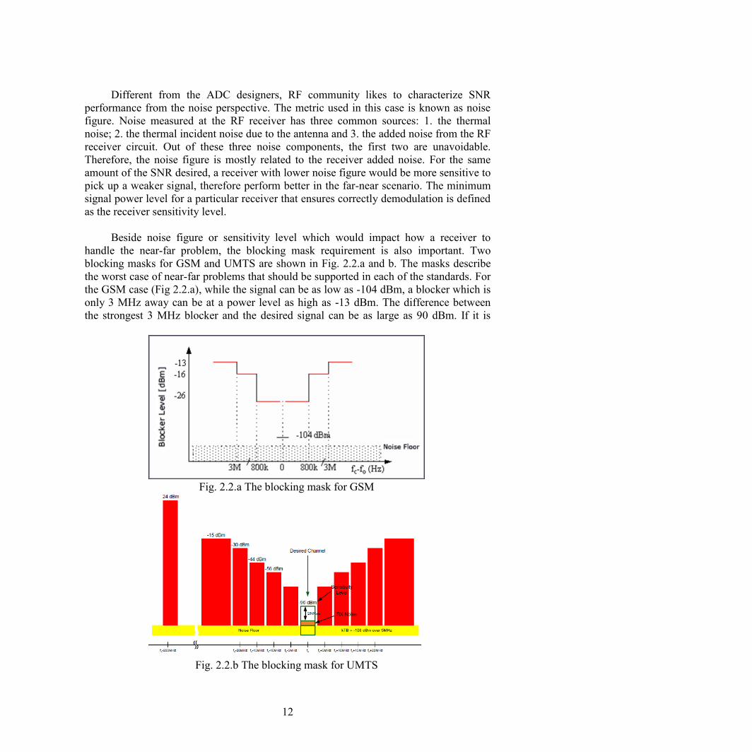
Beside noise figure or sensitivity level which would impact how a receiver to
handle the near-far problem, the blocking mask requirement is also important. Two
blocking masks for GSM and UMTS are shown in Fig. 2.2.a and b. The masks describe
the worst case of near-far problems that should be supported in each of the standards. For
the GSM case (Fig 2.2.a), while the signal can be as low as -104 dBm, a blocker which is
only 3 MHz away can be at a power level as high as -13 dBm. The difference between
the strongest 3 MHz blocker and the desired signal can be as large as 90 dBm. If it is
Fig. 2.2.a The blocking mask for GSM
Fig. 2.2.b The blocking mask for UMTS
13
translated to a voltage swing, the blocker would be on the order of 104 times larger than
the desired signal.
Compared Fig. 2.2.a and Fig 2.2.b, it should be apparent that GSM and UMTS are
quite different from each other. Not only the required receiver sensitivities differ by ~
10dBm, but the blocking masks are different too. Therefore, it poses serious challenges to
software-define radio system, as it needs to meet the sensitivity and the blocking mask
requirement for various standards.
Given this understanding, it helps to explore different strategies in partitioning the
analog and the digital components for the optimal implementation of a software-defined
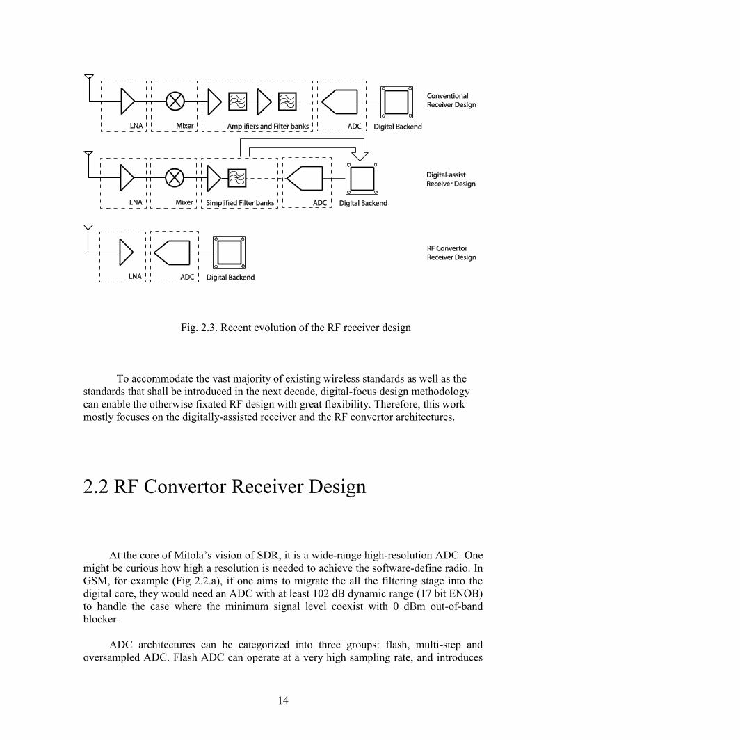
radio system. First off, a conventional type of the receiver structure is introduced.
Classical receiver design consist a series of amplification stages, filter stages and mixing
stages in cascade as shown in Fig. 2.3. For direct-conversion receiver implementation as
shown in Figure 2.3, the system has a LNA to provide early amplification which
improves the noise figure performance. A down-conversion mixer then translates the
signal content from the carrier frequency down to DC or to a low intermediate frequency
(IF). Depending on the actual implementation, the filters might occur prior or after the
mixing stage to meet the particular blocking mask requirement demanded by the
standard. Finally, there is an ADC digitizing the analog signal, and digital output would
then be sent to the DSP for demodulation and further processing. As the desired signal
travels down this mixed-signal path, it is amplified gradually until it satisfies the
minimum SNR requirement demanded by the demodulation process. On the other hand,
the blockers or interferences would be attenuated stage after stage so that the components
in the receiver chain would not be upset by their presence. As the combine result of these
two processes, receiver can handle the near-and-far problem with confidence, and the
received signal can demodulated successively even in the minimum signal level.
One major change in direction in the RF receiver design is in the filtering. The
channel selection filter, is migrated into the digital domain as shown in figure 2.3 thanks
to the technology scaling. Digital assisted design not only helps reduce the silicon area,
but also helps achieve a more flexible design. However, the amount of signal processing
can be shifted into the digital backend is dictated by the achievable dynamic range and
the sampling rate of the ADC. The larger the ADC’s dynamic range can be, more signal
conditioning can be pushed into the digital domain, and hence the RF frontend is more
flexible. From the sampling point of view, if an ADC can sample at faster rate, a less
stringent anti-aliasing filter is required. Taking these two points to extreme, it yields to
Mitola’s vision of the software-defined radio receiver.
14
Fig. 2.3. Recent evolution of the RF receiver design
To accommodate the vast majority of existing wireless standards as well as the
standards that shall be introduced in the next decade, digital-focus design methodology
can enable the otherwise fixated RF design with great flexibility. Therefore, this work
mostly focuses on the digitally-assisted receiver and the RF convertor architectures.
2.2 RF Convertor Receiver Design
At the core of Mitola’s vision of SDR, it is a wide-range high-resolution ADC. One
might be curious how high a resolution is needed to achieve the software-define radio. In
GSM, for example (Fig 2.2.a), if one aims to migrate the all the filtering stage into the
digital core, they would need an ADC with at least 102 dB dynamic range (17 bit ENOB)
to handle the case where the minimum signal level coexist with 0 dBm out-of-band
blocker.
ADC architectures can be categorized into three groups: flash, multi-step and
oversampled ADC. Flash ADC can operate at a very high sampling rate, and introduces

15
the lowest latency among all. However, its resolution is limited and its design is power
hungry. Multi-step ADC such as pipeline and SAR digitizes the input signal in a few
cycles. They are good fit for applications with medium resolution and medium bandwidth
requirement, but they fail to meet the speed and resolution requirements for SDR system.
For a Nyquist-rate ADC design, a one-bit resolution improvement requires four times
more power, therefore, designing a high-speed Nyquist-rate ADC whose resolution is
capable of meeting the near-far requirement is too power hungry to be practical. As the
result, Mitola’s vision of digitizing at the antenna is not realizable.
To circumvent this fundamental issue, one needs to recognize that the ADC doesn’t
need to maintain its high dynamic range over the entire half-Nyquist bandwidth. The high
dynamic range is needed only within the narrow band where the modulated signal
resides. For the rest of the Nyquist bandwidth, the ADC can have a more relaxed
dynamic range. The ADC still has to maintain a large full-scale range over a wide range
of frequencies to handle the out-of-band blocker. This makes oversampling ADC, in
particular ΔΣ ADC, a potent candidate for software-defined radio application.
2.2.1 Overview on ΔΣ ADC Design
ΔΣ ADC is most well-known for its high resolution achieved over a narrow signal
bandwidth in a power efficient manner. Moreover, it also ease on the front-end anti-
aliasing filter requirements, hence reduces the overall power consumptions. There are
many detail references on ΔΣ ADC in the literature [22][23]. For completeness of this
work, a brief overview of ΔΣ ADC is included here.
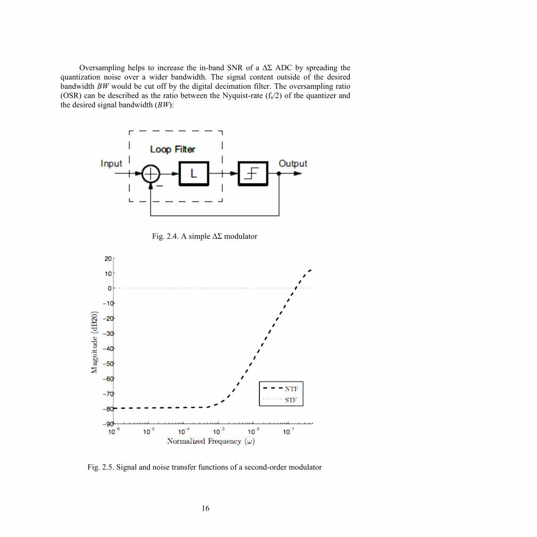
ΔΣ modulator as shown in figure 2.4 features two powerful concepts: oversampling
and noise-shaping. Taking advantage of these two concepts, ΔΣ ADC can achieve a high
resolution even with a one-bit quantizer design.
16
Oversampling helps to increase the in-band SNR of a ΔΣ ADC by spreading the
quantization noise over a wider bandwidth. The signal content outside of the desired
bandwidth BW would be cut off by the digital decimation filter. The oversampling ratio
(OSR) can be described as the ratio between the Nyquist-rate (fs/2) of the quantizer and
the desired signal bandwidth (BW):
Fig. 2.4. A simple ΔΣ modulator
Fig. 2.5. Signal and noise transfer functions of a second-order modulator
17
For a quantizer with N-bit resolution, its SNR is (1.76+6.02N) dB. Since the
quantization noise is spread over a wider bandwidth, if we assume the quantization noise
is white, then the overall in-band SNR with an oversampling ratio can be described as:
As OSR is doubled, the overall SNR would increase by 3 dB.
The overall SNR can be further improved by pushing most of the quantization noise
out of the band of interest, which is known as the noise shaping. Noise shaping is
implemented by enclosing a loop filter inside the ΔΣ modulator loop as shown in the
figure 2.4. This loop filter should have minimum impact on the desired signal, but it high-
pass filters the in-band quantization noise, and pushes them out of the band as
demonstrated in figure 2.5. The actual loop filter implementation varies from design to
design, and it can either take the form of a low-pass structure or a band-pass structure. By
combining the techniques of oversampling and noise shaping, a much larger SNR
improvement can be achieved
Without a loss in generality, assume a low-pass filter is chosen as the ΔΣ loop filter.
The loop filter should have minimum impact on the desired signal, therefore the signal
transfer function (STF) is flat in this case. The loop filter’s low-frequency gain forces the
feedback signal to follow the input signal with high fidelity. The quantization noise
content in those frequencies is rejected by the low-frequency gain of the entire loop
structure. For short, the large loop gain of the feedback system helps to suppress the in
band noise. As the loop gain diminishes at higher frequency, the effect of the noise
suppression degrades as well. Therefore the noise transfer function (NTF) rises as the
frequency increases, as shown in figure 2.5.
For example, in the case from figure 2.5, a second order low-pass filter is chosen as
the ΔΣ loop filter. The STF and the NTF can be described as:
(1)
(2)
18
The STF is truly flat over the entire frequency, and the NTF has a high-pass nature
compared to the low-pass loop filter. Given this particular nature of the NTF, the
quantization noise is lower at the low frequencies, and hence a higher dynamic range can
be assured there. Moreover, NTF has a second order high-pass response, therefore, the
out-of-band quantization noise rises with a 40dB-per-decade slope, which is typically
described as a second–order noise shaping. In such a way, the ΔΣ manages to achieve a
high resolution in a narrow frequency band, while maintaining a high-sampling frequency
which helps to ease the anti-aliasing filter design.
Higher-order ΔΣ ADC enjoys the benefit of higher order noise shaping, therefore,
to achieve the same resolution, lower OSR is required, which helps to reduce the power
consumption of the system and simplify the quantizer and feedback DAC design.
However, higher-order ΔΣ ADCs demand higher-order loop filter, which contains more
poles and zeroes. Just as every other feedback system, it is much harder to maintain the
overall stability when the system becomes more complicated. ADC designers often have
to trade off favorably between the orders of the system with a reasonable OSR. In
general, most of the commercial ΔΣ ADC designs refrain to an order less than five, due to
the stability and complexity reasons.
As mentioned above, ΔΣ ADC’s output spectrum contains not only the desired
signal, but also a wide-frequency of the shaped noise. This suggests its output needs to be
filtered and down-sampled before the digital signal processor can demodulate the desired
signal efficiently. The digital decimation filter can be implemented in the digital domain
without causing too much power consumption. Modern CMOS technology allows for a
very power and area-efficient implementation of such digital design. Even better, digital
decimation filter can scale with the process, which further reduces its impact on the
overall power and area budget.
(3)
(4)

19
2.2.2 ΔΣ ADC in RF Receivers
As discussed earlier, an ADC that meets the SDR requirements needs to have a
high resolution and fast sampling rate at the same time. ΔΣ ADC offers a unique
alternative, compared to other topologies to meet both of these two criteria, while
maintaining a reasonable power and cost budget. ΔΣ ADC is able to avoid the some of
the fundamental trade-offs facing by the Nyquist rate ADC designs.
ΔΣ modulator design is promising for RF receiver design is mostly due to its two
prominent features: oversampling and noise-shaping. Oversampling raises the Nyquist
rate, and hence it eases on the anti-aliasing filter design. For a Nyquist rate ADC design,
increasing the sampling-rate is really challenging, since this ADC needs maintain its
noise floor over the widened bandwidth. To add to the matter, as the ADC can handle a
wider range of input, it is susceptible for the out-of-band interferences, which could be a
few times or order of magnitude bigger than the desired signal. Therefore, the required
dynamic range and sampling speed requirement makes a Nyquist-ADC design highly
impractical.
It is really important to realize that high resolution conversion is not necessary over
the entire frequency range, but only for narrow frequency band of interest, where the
desired signal resides. For frequencies other than that band of interest, the ADC only
needs to tolerate a large input level such as that the large out-of-band blockers are not
going to rail out the ADC. Given these two important observations, ΔΣ ADC truly shines
in the SDR application, as it can provide a high dynamic range only over a narrow
frequency band, while maintaining a high sampling rate. The narrow-band high-
resolution conversion ensures the conversion process of the ΔΣ ADC is as efficient as
possible. Compared to Nyquist-rate designs, where all the signals (both in-band and out-
of-band) are still being converted in high resolution, large amount of the power is wasted
in converting signals which has little use for demodulation process. ΔΣ ADC data
conversion process is much more energy efficient.
Aliasing is a major issue that plagues any type of the ADC design. However, for RF
receiver design, an explicit anti-aliasing filter might not be necessary. First, RF
components such as antenna SAW filters, TR switches and duplexers all have limited
operational bandwidth. ΔΣ ADC’s sampling rate is often much higher than the narrow
band of interest, then, the first aliasing Nyquist zone is quite faraway. Hence, the limited
operational bandwidth of various RF components can serve as implicit filtering for
aliasing contents. Even better, bondwire has limited operation bandwidth as well, which
further helps to suppress the aliasing content. Moreover, as shall be discussed later in this
work, other techniques can effectively alleviate the issue of aliasing in an ADC-based RF
receiver design. Overall, the removal of an explicit analog anti-aliasing filter not only
helps to maintain a better power and area budget of the overall design, but it also enables
great flexibility of the design, as the signal bandwidth is no longer explicitly defined in
the analog domain. The final signal selection can be pushed into the digital domain, in the
20
form of the application of digital filters. Combined with a programmable digital system
such as FPGA, it allows a possibility of on-the-fly re-programming the digital filters to
accommodate the change of signal bandwidths and applications. This feature is very
amenable and appealing as a concept for reconfigurable RF receiver.
2.3 Digitally-Assisted Receiver Architecture
The beauty of the digitally-assisted Receiver is that a part of the filtering network
is shifted into the digital domain. The analog/RF components can be reduced to its
minimum to enhance the flexibility and better performance vs. power tradeoff for the
overall system. To carry this idea to the extreme, it will very well be an ideal ADC that
fits the idea of software-defined radio. Throughout the past decade, technology scaling
has been marching into the sub-micrometer region, and it enables devices with sizes 100th
of micrometers to come into production. At this point of time, realization of devices size
even down to single digit nanometer is not that far at all. This improvement in the process
shrinking not only makes the digital backend more capable and power efficient than any
time before, but also allows many mixed signal blocks, such as ADC, to evolve at the
same time. In particular, ADC design for wireless applications has experienced major
change in the past decade. In most of the wireless applications, the once dominant
Pipeline architecture has become obsolete. Its throne is now claimed by architectures
such as ΔΣ ADC and SAR ADC. SAR ADC architecture scales more naturally with the
technology shrinking, while the ΔΣ ADC draws great benefits from a more capable
digital backend enabled by the latest technology improvement. In the literature, SAR
ADCs and ΔΣ ADCs have been reported efficiency that is ten times better than Pipeline
ADCs. Because of the more powerful digital core as well as a more capable data
convertor, the conventional way of partitioning between the analog/RF domain and
digital domain is obsolete, and cannot provide the best performance vs. power tradeoff. In
the recent decade, a great amount of research effort has been made in reshaping the
boundary between the digital and analog/RF. Many analog/RF components, which used
to be deemed as essential or critical for the applications, have been removed from the
receiver chain successively. The overall result is a much simpler design with much better
power efficiency.
2.3.1 Passive Mixer-first Receiver Design
The passive mixer-first receiver design centers on the idea of the passive mixer,
which has been reported in 2000 [57][58]. For a fairly long time, active Gilbert mixers
have been the mainstay for the integrated receiver system, because of their gain
performance. However, they suffer from high flicker noise. Passive mixers, on the other
hand, has higher conversion losses but outstanding flicker noise performance [119][120].
Several studies have addressed passive mixer design convers in great detail from the
21
perspective of noise, dc offset, second-order distortion and third-order
distortion[120][121][122][123]. Over the years, it has become the mainstream design for
modern commercial integrated receiver systems [59][60].
Also, it has been shown that by utilizing a multiple non-overlapping LO
waveforms, the passive mixer designs can be further optimized [58][60][63][64][65].
Recent mixer-first receiver designs have demonstrated that the architecture can achieve
excellent noise and linearity performance: reference [25] has shown a sample design with
a record-high 25 dBm IIP3, while in [68] a mixer-first system with a 1.9 dB noise figure
is reported with the aid of noise cancellation.
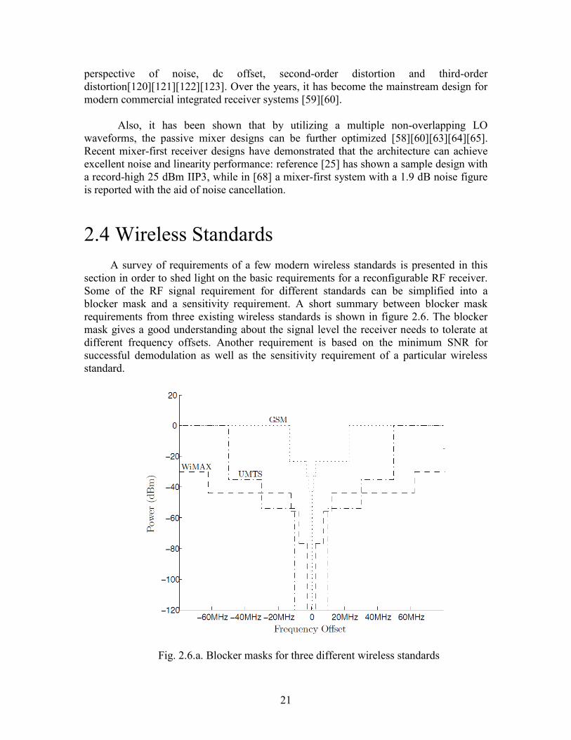
2.4 Wireless Standards
A survey of requirements of a few modern wireless standards is presented in this
section in order to shed light on the basic requirements for a reconfigurable RF receiver.
Some of the RF signal requirement for different standards can be simplified into a
blocker mask and a sensitivity requirement. A short summary between blocker mask
requirements from three existing wireless standards is shown in figure 2.6. The blocker
mask gives a good understanding about the signal level the receiver needs to tolerate at
different frequency offsets. Another requirement is based on the minimum SNR for
successful demodulation as well as the sensitivity requirement of a particular wireless
standard.
Fig. 2.6.a. Blocker masks for three different wireless standards
22
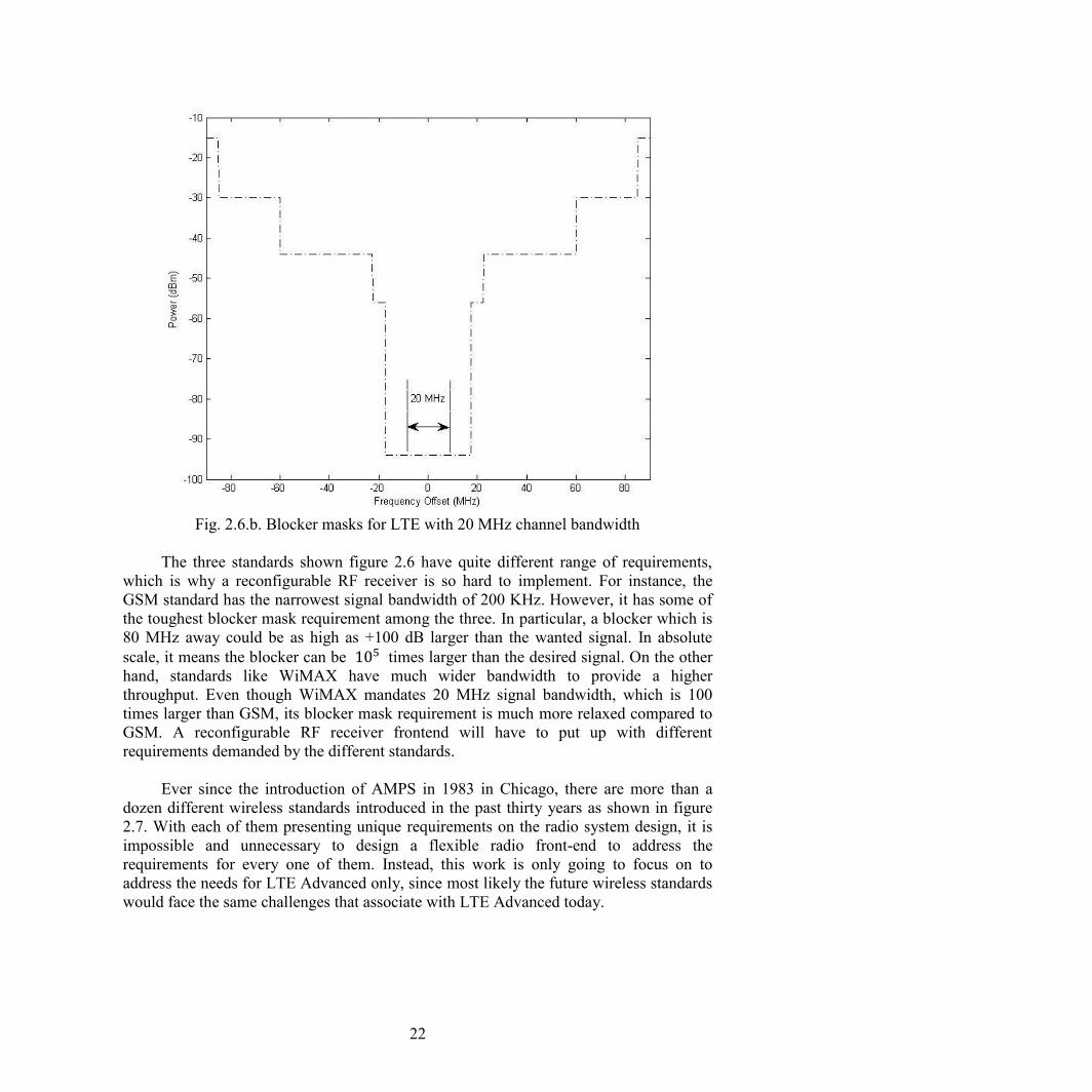
Fig. 2.6.b. Blocker masks for LTE with 20 MHz channel bandwidth
The three standards shown figure 2.6 have quite different range of requirements,
which is why a reconfigurable RF receiver is so hard to implement. For instance, the
GSM standard has the narrowest signal bandwidth of 200 KHz. However, it has some of
the toughest blocker mask requirement among the three. In particular, a blocker which is
80 MHz away could be as high as +100 dB larger than the wanted signal. In absolute
scale, it means the blocker can be times larger than the desired signal. On the other
hand, standards like WiMAX have much wider bandwidth to provide a higher
throughput. Even though WiMAX mandates 20 MHz signal bandwidth, which is 100
times larger than GSM, its blocker mask requirement is much more relaxed compared to
GSM. A reconfigurable RF receiver frontend will have to put up with different
requirements demanded by the different standards.
Ever since the introduction of AMPS in 1983 in Chicago, there are more than a
dozen different wireless standards introduced in the past thirty years as shown in figure
2.7. With each of them presenting unique requirements on the radio system design, it is
impossible and unnecessary to design a flexible radio front-end to address the
requirements for every one of them. Instead, this work is only going to focus on to
address the needs for LTE Advanced only, since most likely the future wireless standards
would face the same challenges that associate with LTE Advanced today.
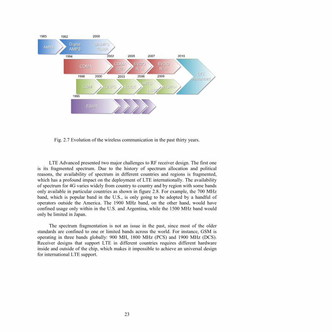
23
Fig. 2.7 Evolution of the wireless communication in the past thirty years.
LTE Advanced presented two major challenges to RF receiver design. The first one
is its fragmented spectrum. Due to the history of spectrum allocation and political
reasons, the availability of spectrum in different countries and regions is fragmented,
which has a profound impact on the deployment of LTE internationally. The availability
of spectrum for 4G varies widely from country to country and by region with some bands
only available in particular countries as shown in figure 2.8. For example, the 700 MHz
band, which is popular band in the U.S., is only going to be adopted by a handful of
operators outside the America. The 1900 MHz band, on the other hand, would have
confined usage only within in the U.S. and Argentina, while the 1500 MHz band would
only be limited in Japan.
The spectrum fragmentation is not an issue in the past, since most of the older
standards are confined to one or limited bands across the world. For instance, GSM is
operating in three bands globally: 900 MH, 1800 MHz (PCS) and 1900 MHz (DCS).
Receiver designs that support LTE in different countries requires different hardware
inside and outside of the chip, which makes it impossible to achieve an universal design
for international LTE support.
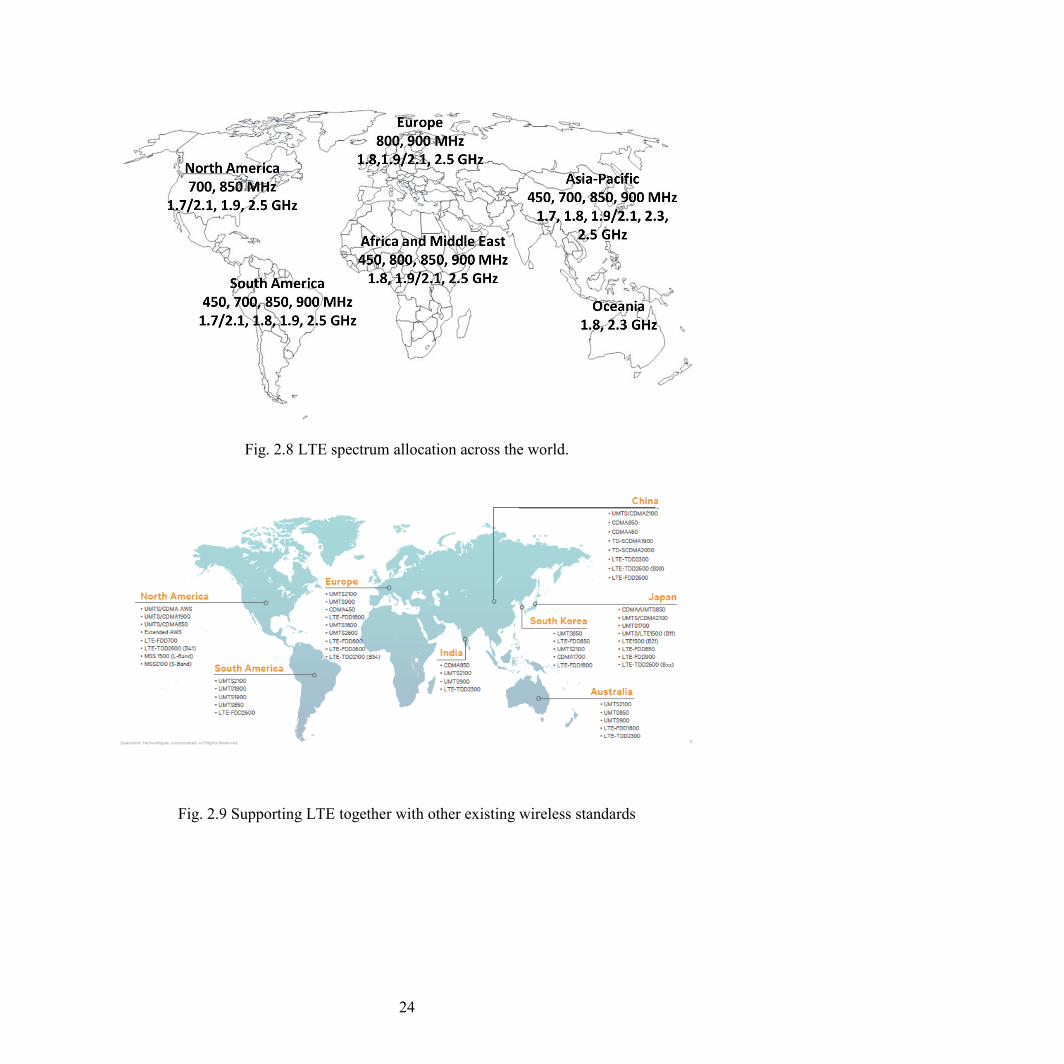
24
Fig. 2.8 LTE spectrum allocation across the world.
Fig. 2.9 Supporting LTE together with other existing wireless standards
25
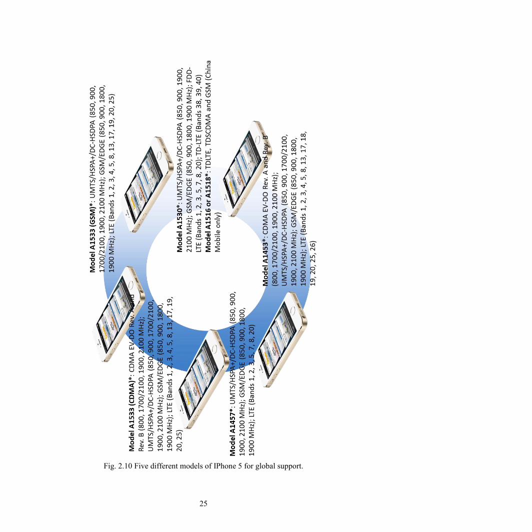
Fig. 2.10 Five different models of IPhone 5 for global support.

26
The problem gets even worse, when we consider the backward compatibility for
legacy wireless standards. Figure 2.9 shows an example of what different wireless
standards need to be supported for different part of the world. There are a total of over 40
different RF bands required. As the result, mobile device manufacturers are facing
serious challenges in supporting LTE. The highly fragmented spectrum requirement
makes it impossible for standardizing devices for a global market. Virtually all countries
regulate their radio spectrum in a different way and large portions of the spectrum that
could be aggregated for LTE are already in use for other devices or services. Therefore,
given the technology limitation, one device for one dedicated region seems to be the cell-
phone manufactures best strategy so far. For example, the iPhone 5 has five different
models to provide the support for different regions and different carriers as shown in
figure 2.10. For the reason given above, there are two models dedicated to the U.S.
market alone to provide coverage for AT&T and Verizon Wireless.
LTE Advanced provides additional improvement in user data rates through carrier
aggregation (CA). LTE Advanced can aggregate up to five carriers (up to 100 MHz
bandwidth) to a single user and increase capacity for different applications as illustrated
in figure 2.11. As a first step, the current LTE Advanced (Cat 4) can support the
aggregation of two 10 MHz carriers, which allows a peak 150 Mbps data rate.
Fig. 2.11 Five sub-carrier carrier aggregation to generate a higher bandwidth.
27
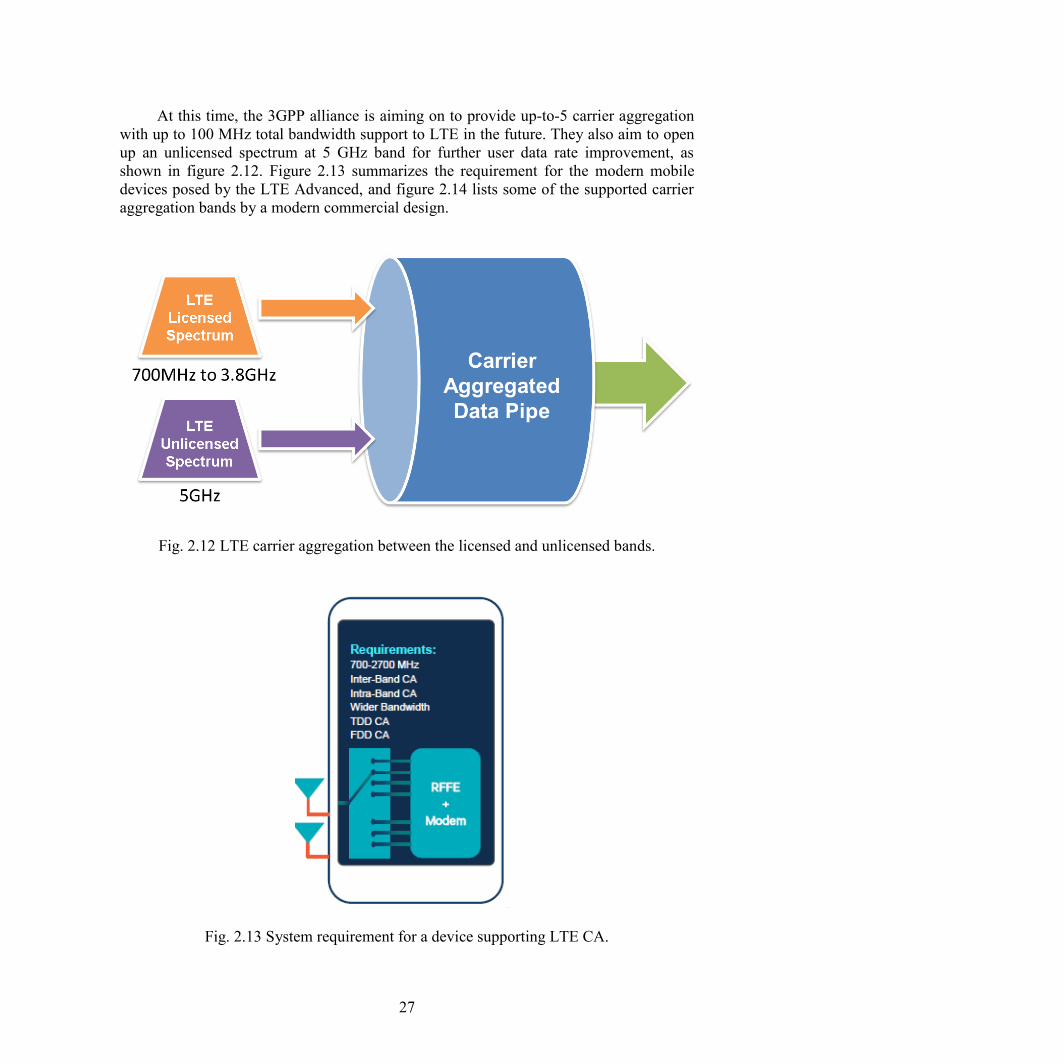
At this time, the 3GPP alliance is aiming on to provide up-to-5 carrier aggregation
with up to 100 MHz total bandwidth support to LTE in the future. They also aim to open
up an unlicensed spectrum at 5 GHz band for further user data rate improvement, as
shown in figure 2.12. Figure 2.13 summarizes the requirement for the modern mobile
devices posed by the LTE Advanced, and figure 2.14 lists some of the supported carrier
aggregation bands by a modern commercial design.
Fig. 2.12 LTE carrier aggregation between the licensed and unlicensed bands.
Fig. 2.13 System requirement for a device supporting LTE CA.
28
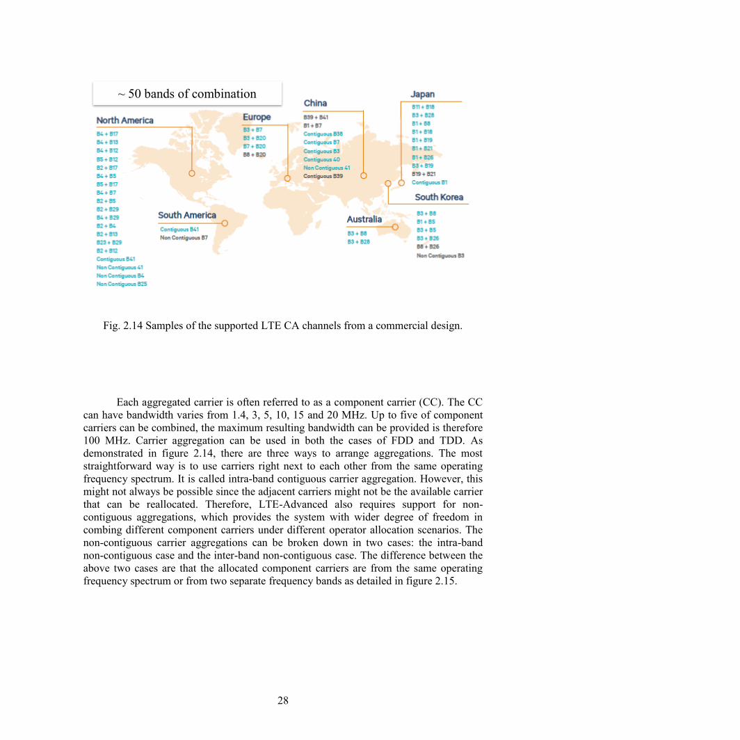
Fig. 2.14 Samples of the supported LTE CA channels from a commercial design.
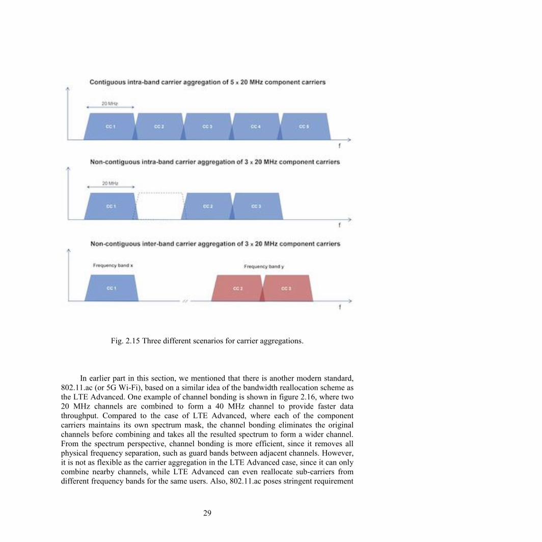
Each aggregated carrier is often referred to as a component carrier (CC). The CC
can have bandwidth varies from 1.4, 3, 5, 10, 15 and 20 MHz. Up to five of component
carriers can be combined, the maximum resulting bandwidth can be provided is therefore
100 MHz. Carrier aggregation can be used in both the cases of FDD and TDD. As
demonstrated in figure 2.14, there are three ways to arrange aggregations. The most
straightforward way is to use carriers right next to each other from the same operating
frequency spectrum. It is called intra-band contiguous carrier aggregation. However, this
might not always be possible since the adjacent carriers might not be the available carrier
that can be reallocated. Therefore, LTE-Advanced also requires support for non-
contiguous aggregations, which provides the system with wider degree of freedom in
combing different component carriers under different operator allocation scenarios. The
non-contiguous carrier aggregations can be broken down in two cases: the intra-band
non-contiguous case and the inter-band non-contiguous case. The difference between the
above two cases are that the allocated component carriers are from the same operating
frequency spectrum or from two separate frequency bands as detailed in figure 2.15.
~ 50 bands of combination
29
Fig. 2.15 Three different scenarios for carrier aggregations.
In earlier part in this section, we mentioned that there is another modern standard,
802.11.ac (or 5G Wi-Fi), based on a similar idea of the bandwidth reallocation scheme as
the LTE Advanced. One example of channel bonding is shown in figure 2.16, where two
20 MHz channels are combined to form a 40 MHz channel to provide faster data
throughput. Compared to the case of LTE Advanced, where each of the component
carriers maintains its own spectrum mask, the channel bonding eliminates the original
channels before combining and takes all the resulted spectrum to form a wider channel.
From the spectrum perspective, channel bonding is more efficient, since it removes all
physical frequency separation, such as guard bands between adjacent channels. However,
it is not as flexible as the carrier aggregation in the LTE Advanced case, since it can only
combine nearby channels, while LTE Advanced can even reallocate sub-carriers from
different frequency bands for the same users. Also, 802.11.ac poses stringent requirement
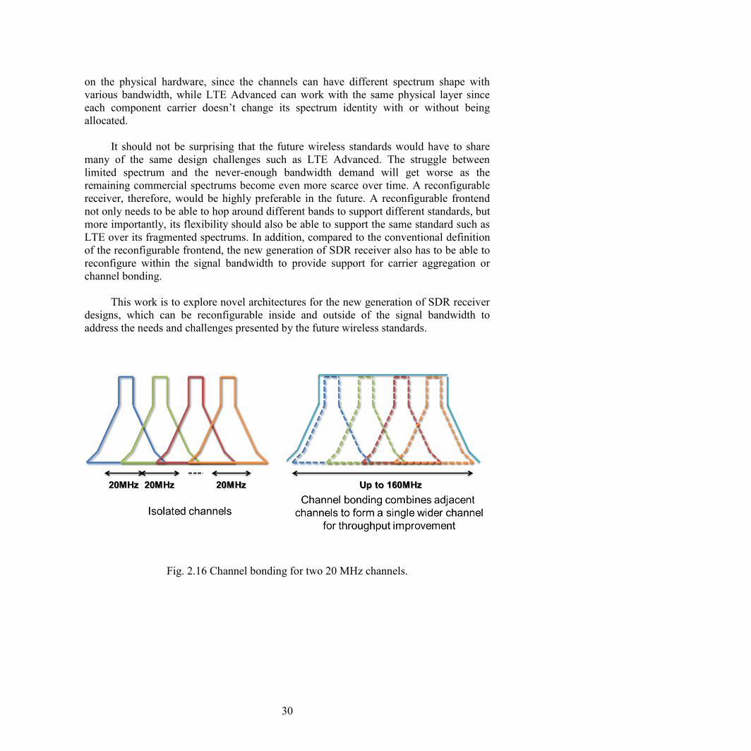
30
on the physical hardware, since the channels can have different spectrum shape with
various bandwidth, while LTE Advanced can work with the same physical layer since
each component carrier doesn’t change its spectrum identity with or without being
allocated.
It should not be surprising that the future wireless standards would have to share
many of the same design challenges such as LTE Advanced. The struggle between
limited spectrum and the never-enough bandwidth demand will get worse as the
remaining commercial spectrums become even more scarce over time. A reconfigurable
receiver, therefore, would be highly preferable in the future. A reconfigurable frontend
not only needs to be able to hop around different bands to support different standards, but
more importantly, its flexibility should also be able to support the same standard such as
LTE over its fragmented spectrums. In addition, compared to the conventional definition
of the reconfigurable frontend, the new generation of SDR receiver also has to be able to
reconfigure within the signal bandwidth to provide support for carrier aggregation or
channel bonding.
This work is to explore novel architectures for the new generation of SDR receiver
designs, which can be reconfigurable inside and outside of the signal bandwidth to
address the needs and challenges presented by the future wireless standards.
Fig. 2.16 Channel bonding for two 20 MHz channels.
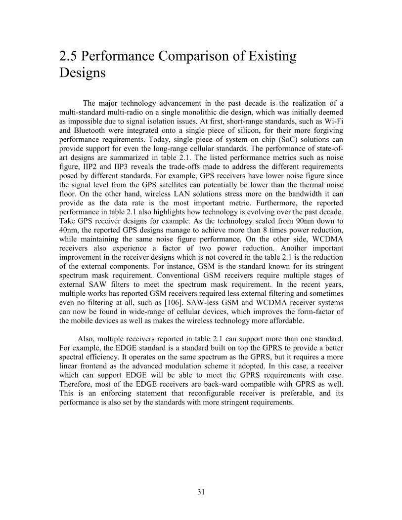
31
2.5 Performance Comparison of Existing
Designs
The major technology advancement in the past decade is the realization of a
multi-standard multi-radio on a single monolithic die design, which was initially deemed
as impossible due to signal isolation issues. At first, short-range standards, such as Wi-Fi
and Bluetooth were integrated onto a single piece of silicon, for their more forgiving
performance requirements. Today, single piece of system on chip (SoC) solutions can
provide support for even the long-range cellular standards. The performance of state-of-
art designs are summarized in table 2.1. The listed performance metrics such as noise
figure, IIP2 and IIP3 reveals the trade-offs made to address the different requirements
posed by different standards. For example, GPS receivers have lower noise figure since
the signal level from the GPS satellites can potentially be lower than the thermal noise
floor. On the other hand, wireless LAN solutions stress more on the bandwidth it can
provide as the data rate is the most important metric. Furthermore, the reported
performance in table 2.1 also highlights how technology is evolving over the past decade.
Take GPS receiver designs for example. As the technology scaled from 90nm down to
40nm, the reported GPS designs manage to achieve more than 8 times power reduction,
while maintaining the same noise figure performance. On the other side, WCDMA
receivers also experience a factor of two power reduction. Another important
improvement in the receiver designs which is not covered in the table 2.1 is the reduction
of the external components. For instance, GSM is the standard known for its stringent
spectrum mask requirement. Conventional GSM receivers require multiple stages of
external SAW filters to meet the spectrum mask requirement. In the recent years,
multiple works has reported GSM receivers required less external filtering and sometimes
even no filtering at all, such as [106]. SAW-less GSM and WCDMA receiver systems
can now be found in wide-range of cellular devices, which improves the form-factor of
the mobile devices as well as makes the wireless technology more affordable.
Also, multiple receivers reported in table 2.1 can support more than one standard.
For example, the EDGE standard is a standard built on top the GPRS to provide a better
spectral efficiency. It operates on the same spectrum as the GPRS, but it requires a more
linear frontend as the advanced modulation scheme it adopted. In this case, a receiver
which can support EDGE will be able to meet the GPRS requirements with ease.
Therefore, most of the EDGE receivers are back-ward compatible with GPRS as well.
This is an enforcing statement that reconfigurable receiver is preferable, and its
performance is also set by the standards with more stringent requirements.
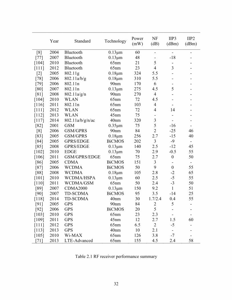
32
Year Standard Technology Power
(mW)
NF
(dB)
IIP3
(dBm)
IIP2
(dBm)
[8] 2004 Bluetooth 0.13μm 60 - - -
[77] 2007 Bluetooth 0.13μm 48 - -18 -
[104] 2010 Bluetooth 65nm 21 5 - -
[111] 2012 Bluetooth 65nm 23 4 3 -
[2] 2005 802.11g 0.18μm 324 5.5 - -
[78] 2006 802.11a/b/g 0.18μm 310 5.5 - -
[79] 2006 802.11n 90nm 170 6 - -
[80] 2007 802.11n 0.13μm 275 4.5 5 -
[81] 2008 802.11a/g/n 90nm 270 4 - -
[104] 2010 WLAN 65nm 72 4.5 - -
[116] 2011 802.11n 65nm 103 4 - -
[111] 2012 WLAN 65nm 72 4 14 -
[112] 2013 WLAN 45nm 75 - - -
[117] 2014 802.11a/b/g/n/ac 40nm 320 3 - -
[82] 2001 GSM 0.35μm 75 5 -16 -
[8] 2006 GSM/GPRS 90nm 84 2 -25 46
[83] 2005 GSM/GPRS 0.18μm 256 2.7 -15 40
[84] 2005 GPRS/EDGE BiCMOS 202 3 -9 -
[85] 2008 GPRS/EDGE 0.13μm 140 2.5 -12 45
[102] 2010 EDGE 0.13μm 70 2.9 -0.5 55
[106] 2011 GSM/GPRS/EDGE 65nm 75 2.7 0 50
[86] 2005 CDMA BiCMOS 151 3 - -
[87] 2006 WCDMA BiCMOS 50 9 0 55
[88] 2008 WCDMA 0.18μm 105 2.8 -2 65
[101] 2010 WCDMA/HSPA 0.13μm 60 2.5 -5 55
[110] 2011 WCDMA/GSM 65nm 50 2.4 -3 50
[89] 2007 CDMA2000 0.13μm 150 9.2 1 51
[90] 2007 TD-SCDMA BiCMOS 95 3.5 -14 25
[118] 2014 TD-SCDMA 40nm 30 1.7/2.4 0.4 55
[91] 2005 GPS 90nm 84 2 5 -
[92] 2006 GPS BiCMOS 20 5 - -
[103] 2010 GPS 65nm 23 2.3 - -
[109] 2011 GPS 45nm 12 2.7 1.5 60
[111] 2012 GPS 65nm 6.5 2 -5 -
[113] 2013 GPS 40nm 10 2.1 - -
[105] 2010 Wi-MAX 65nm 126 3.8 -7 -
[71] 2013 LTE-Advanced 65nm 155 4.5 2.4 58
Table 2.1 RF receiver performance summary
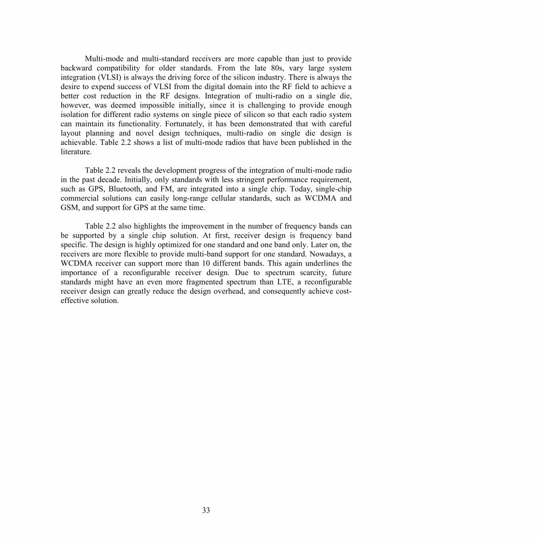
33
Multi-mode and multi-standard receivers are more capable than just to provide
backward compatibility for older standards. From the late 80s, vary large system
integration (VLSI) is always the driving force of the silicon industry. There is always the
desire to expend success of VLSI from the digital domain into the RF field to achieve a
better cost reduction in the RF designs. Integration of multi-radio on a single die,
however, was deemed impossible initially, since it is challenging to provide enough
isolation for different radio systems on single piece of silicon so that each radio system
can maintain its functionality. Fortunately, it has been demonstrated that with careful
layout planning and novel design techniques, multi-radio on single die design is
achievable. Table 2.2 shows a list of multi-mode radios that have been published in the
literature.
Table 2.2 reveals the development progress of the integration of multi-mode radio
in the past decade. Initially, only standards with less stringent performance requirement,
such as GPS, Bluetooth, and FM, are integrated into a single chip. Today, single-chip
commercial solutions can easily long-range cellular standards, such as WCDMA and
GSM, and support for GPS at the same time.
Table 2.2 also highlights the improvement in the number of frequency bands can
be supported by a single chip solution. At first, receiver design is frequency band
specific. The design is highly optimized for one standard and one band only. Later on, the
receivers are more flexible to provide multi-band support for one standard. Nowadays, a
WCDMA receiver can support more than 10 different bands. This again underlines the
importance of a reconfigurable receiver design. Due to spectrum scarcity, future
standards might have an even more fragmented spectrum than LTE, a reconfigurable
receiver design can greatly reduce the design overhead, and consequently achieve cost-
effective solution.
34
Entry Supported Standards Frequency Bands
[93] Broadcom BRCM 2075 Bluetooth (EDR)
GPS
FM
1
1
1
[94] Broadcom BRCM 4329 802.11n
Bluetooth (EDR)
FM
2
1
1
[104] Broadcom BRCM (2010) 802.11a/b/g/n
Bluetooth (EDR)
FM
2
1
1
[95] Marvell (2009) 802.11
WiMAX
1
1
[117] Marvell (2014) 3-stream 802.11a/b/g/n/ac
MIMO
6
[96] Freescale WCDMA/HSDPA
GSM/GPRS/EDGE
10
4
[97] TI GSM/GPRS/EDGE
CDMA2000
3
1
[112] TI (2013) 802.11n 2X2 b/g-band
802.11n 2X2 a-band
2
1
[98] Skyworks WCDMA/HSDPA/HSUPA
GSM/GPRS/EDGE
11
4
[99] Qualcomm (2009) WCDMA/HSDPA/HSUPA
GSM/GPRS/EDGE
GPS
10
4
1
[108] Qualcomm (2011) WCDMA/HSDPA/HSUPA
GSM/GPRS/EDGE
GPS
8
4
1
[116] Atheros (2011) 3 Stream 802.11n MIMO 6
[107] ST-Ericsson (2011) WCDMA
EDGE
9
4
[111] MediaTek (2012) WiFi a/b/g/n
Bluetooth
FM
GPS
-
-
-
-
[118] MediaTek (2014) 2G/3G TD-SCDMA 7
[71] Ericsson (2013) LTE Advanced
with up to 3 carrier
aggregations
2
Table 2.2. A summary for modern multi-mode multi-radio designs.
35
2.5.1 Software-Defined Radio Implementation
Last but not the least, there are also a number of demonstrations of software-
defined radio implementations reported in the literature, such as [102][27][66]. All the
designs have flexible forward signal paths that can be reconfigured in different ways. All
of the designs employ a single-down-conversion architecture followed by a series of
baseband filters where the filters’ corner frequencies can be adjusted to support different
modulation scheme used by the different standards.
36
Chapter 3
ΔΣ Receiver System Architecture
3.1. Introduction
Continued evolution of wideband wireless communications drives the need for
flexible receivers capable of multi-mode, multi-standard operation [27][28]. A universal
4G-LTE device, for example, is anticipated to operate from 450 MHz to 3800 MHz with
varying bandwidths. A downconverting analog-to-digital converter (ADC) is an
architecture capable of such operation [29][30]. By embedding the mixer inside the
feedback loop, a highly linear design is achievable. By utilizing a low-noise
transconductance amplifier (LNTA) in front of the ADC, this architecture can perform a
low noise direct RF-to-digital conversion. The center frequency is tuned by an external
oscillator, and the bandwidth is set by the decimation filter. With large dynamic range,
this architecture enables the ADC to migrate closer to the antenna, enabling many signal
conditioning features to be implemented in the digital domain, thus benefiting from
technology scaling.
While the direct-conversion architecture is still prevalent in commercial mobile
handsets, significant research effort has been shifted towards novel schemes that employ
bandpass or downconverting ADCs. Previous implementations of downconverting
receivers with switched-capacitor loop filters have demonstrated wide-tuning range or
high dynamic range, but not both [29][30]. In general, the dynamic range has been
limited by the clock jitter injected at high frequencies from the feedback digital-to-analog
converter (DAC). Jitter directly degrades the SNDR of the receiver, since it cannot be
distinguished from input noise. A non-return-to-zero (NRZ) signal waveform helps
reduce the jitter sensitivity by reducing the transitions, while a multi-level DAC improves
the jitter immunity by reducing the transition steps. However, both techniques are
challenging to implement at high frequencies. This thesis demonstrates a system that
achieves a high dynamic range together with a wide-tuning range, enabled by the
implementation of a four-level NRZ DAC. The overall system linearity is further
enhanced by a highly-linear class-AB LNTA.
This chapter is organized as follows. Section 3.2 discusses various architecture
design tradeoffs in order to motivate the choices made in this design. Section 3.3 presents
37
circuit implementation details, and Section 3.4 presents measurement results. The chapter
is concluded in Section 3.5.
3.2 Receiver Architecture
In the following discussion, various system architectures are evaluated and
compared, and the impact of clock jitter is studied and analyzied. In addition, a
behavioral model of a current-mode integration sampler (CMIS) mixer is derived.
Finally, an architecture capable of addressing the desired specifications is proposed.
3.2.1 System Level Design
To meet the requirements of software-defined radio (SDR) applications, an ADC
has to meet two major challenges. The first is that its dynamic range has to be large
enough to process the input signal together with the blockers. The other is that it needs to
downconvert the input signal from the carrier frequency to baseband. A bandpass ΔΣ
ADC Fig. 1 is seemingly an ideal candidate for this application. However its design
requires resonators with high quality factors, which are difficult to realize in CMOS
technology. Passive resonator designs offer higher Q, but come with a large area
overhead and limited tuning range. On the other hand, active resonators are tunable but
suffer from limited quality factors. In addition, active designs lead to large power
overhead and limit the system’s linearity.
An alternative design of a bandpass ΔΣ system is proposed in [32]. By summing the
feedback signals from the two interleaved channels, it forms a bandpass feedback
structure as illustrated in Fig. 2(a). Taking advantage the idea of current mode integration
sampling which would be elaborated later, the sampler in Fig. 3.2(a) can be transformed
into a mixer and be moved inside of the ΔΣ loop as in Fig. 3.2(b). The bandpass feedback
suppresses the swing at the RF nodes, and enhances the linearity of both the LNTA as
well as the baseband ΔΣ ADCs). The two channels of the ΔΣ ADCs also serve to
oversample the input data by a factor of two, thus providing a 3dB SNR improvement.
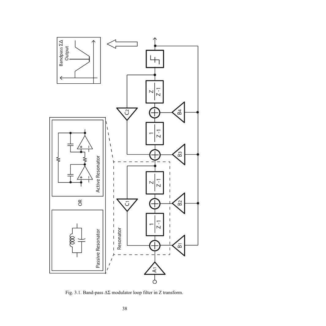
38
Fig. 3.1. Band-pass ΔΣ modulator loop filter in Z transform.
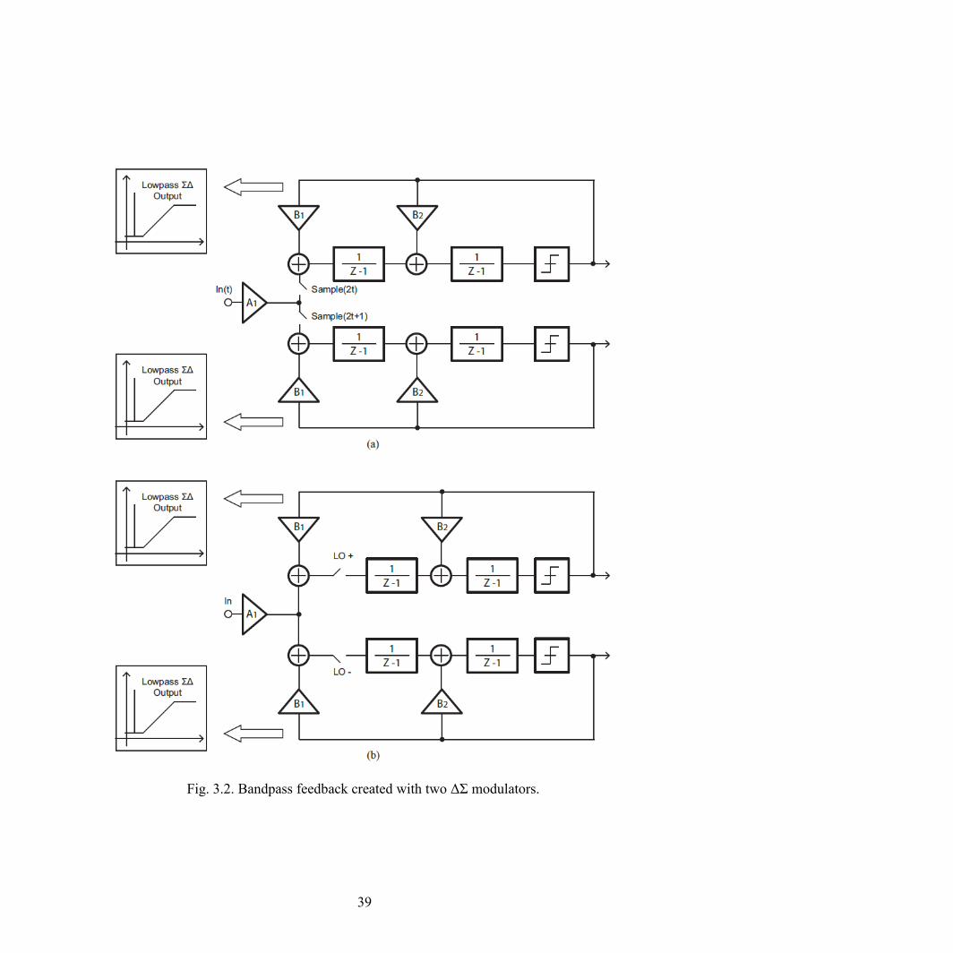
39
Fig. 3.2. Bandpass feedback created with two ΔΣ modulators.
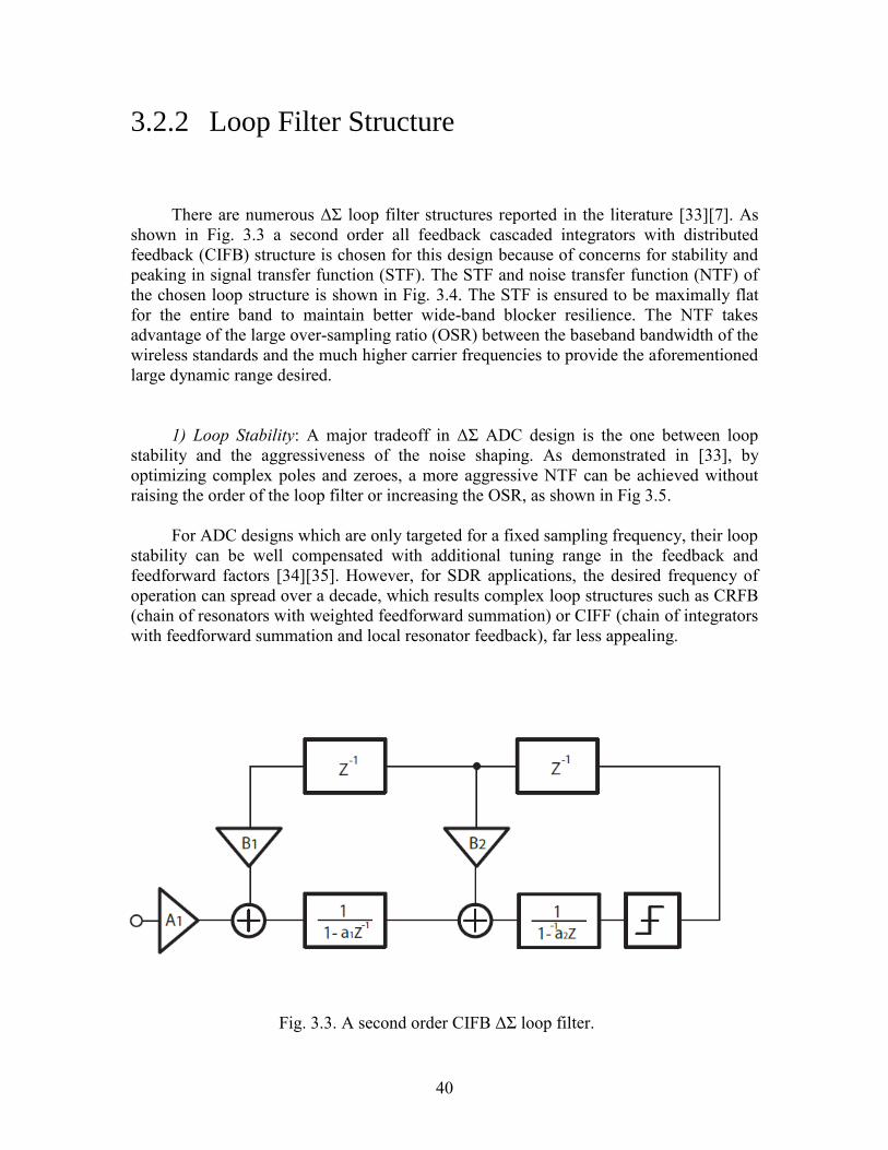
40
3.2.2 Loop Filter Structure
There are numerous ΔΣ loop filter structures reported in the literature [33][7]. As
shown in Fig. 3.3 a second order all feedback cascaded integrators with distributed
feedback (CIFB) structure is chosen for this design because of concerns for stability and
peaking in signal transfer function (STF). The STF and noise transfer function (NTF) of
the chosen loop structure is shown in Fig. 3.4. The STF is ensured to be maximally flat
for the entire band to maintain better wide-band blocker resilience. The NTF takes
advantage of the large over-sampling ratio (OSR) between the baseband bandwidth of the
wireless standards and the much higher carrier frequencies to provide the aforementioned
large dynamic range desired.
1) Loop Stability: A major tradeoff in ΔΣ ADC design is the one between loop
stability and the aggressiveness of the noise shaping. As demonstrated in [33], by
optimizing complex poles and zeroes, a more aggressive NTF can be achieved without
raising the order of the loop filter or increasing the OSR, as shown in Fig 3.5.
For ADC designs which are only targeted for a fixed sampling frequency, their loop
stability can be well compensated with additional tuning range in the feedback and
feedforward factors [34][35]. However, for SDR applications, the desired frequency of
operation can spread over a decade, which results complex loop structures such as CRFB
(chain of resonators with weighted feedforward summation) or CIFF (chain of integrators
with feedforward summation and local resonator feedback), far less appealing.
Fig. 3.3. A second order CIFB ΔΣ loop filter.
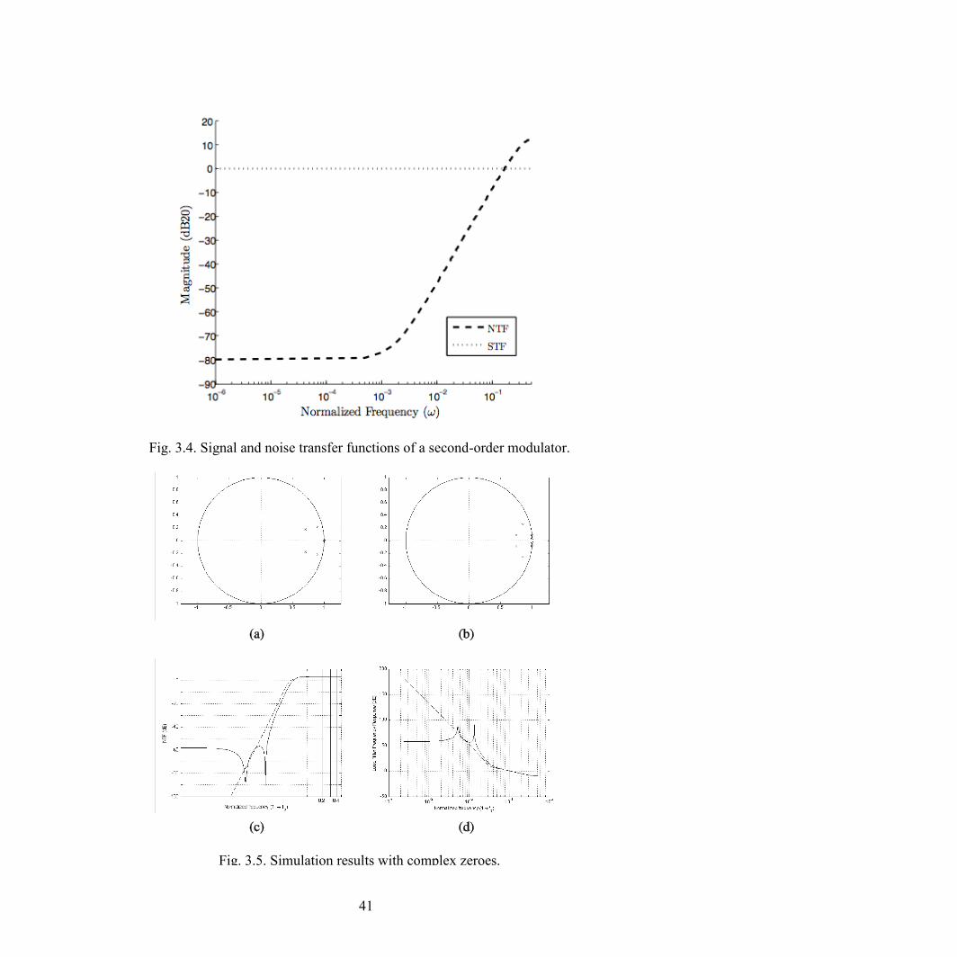
41
Fig. 3.4. Signal and noise transfer functions of a second-order modulator.
Fig. 3.5. Simulation results with complex zeroes.
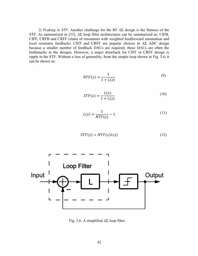
42
2) Peaking in STF: Another challenge for the RF ΔΣ design is the flatness of the
STF. As summarized in [33], ΔΣ loop filter architectures can be summarized as: CIFB,
CIFF, CRFB and CRFF (chain of resonators with weighted feedforward summation and
local resonator feedback). CIFF and CRFF are popular choices in ΔΣ ADC design
because a smaller number of feedback DACs are required; these DACs are often the
bottlenecks in the designs. However, a major drawback for CIFF or CRFF design is
ripple in the STF. Without a loss of generality, from the simple loop shown in Fig. 3.6, it
can be shown as:
Fig. 3.6. A simplified ΔΣ loop filter.
(9)
(10)
(11)
(12)
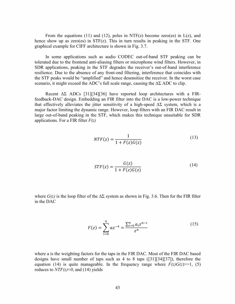
43
From the equations (11) and (12), poles in NTF(z) become zero(es) in L(z), and
hence show up as zero(es) in STF(z). This in turn results in peaking in the STF. One
graphical example for CIFF architecture is shown in Fig. 3.7.
In some applications such as audio CODEC out-of-band STF peaking can be
tolerated due to the frontend anti-aliasing filters or microphone wind filters. However, in
SDR applications, peaking in the STF degrades the receiver’s out-of-band interference
resilience. Due to the absence of any front-end filtering, interference that coincides with
the STF peaks would be “amplified” and hence desensitize the receiver. In the worst case
scenario, it might exceed the ADC’s full scale range, causing the ΔΣ ADC to clip.
Recent ΔΣ ADCs [31][34][36] have reported loop architectures with a FIR-
feedback-DAC design. Embedding an FIR filter into the DAC is a low-power technique
that effectively alleviates the jitter sensitivity of a high-speed ΔΣ system, which is a
major factor limiting the dynamic range. However, loop filters with an FIR DAC result in
large out-of-band peaking in the STF, which makes this technique unsuitable for SDR
applications. For a FIR filter F(z)
where G(z) is the loop filter of the ΔΣ system as shown in Fig. 3.6. Then for the FIR filter
in the DAC
∑
∑
where a is the weighting factors for the taps in the FIR DAC. Most of the FIR DAC based
designs have small number of taps such as 4 to 8 taps ([31][34][37]), therefore the
equation (14) is quite manageable. In the frequency range where F(z)G(z)>>1, (5)
reduces to NTF(z)≈0, and (14) yields
(13)
(14)
(15)
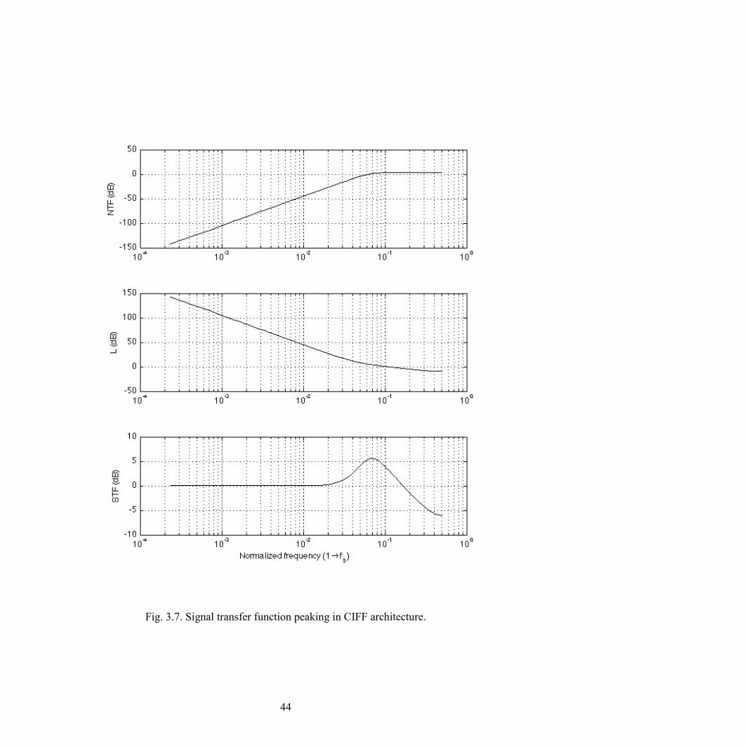
44
Fig. 3.7. Signal transfer function peaking in CIFF architecture.
45
In general, F(z)G(z)>>1at low frequency, since NTF(z) should filter out most of the
quantization noise at the low frequency. On the other hand, STF would be flat if F(z) is
just a short. Or by (14), then
∑
Since F(z) is a FIR function, it has nulls at different frequencies. By (17), these
nulls results in peaking in the STF. The actual height of such peaks relates to the loop
structure as well as the number of taps in the FIR filter. In [34][36], peaking levels higher
than 10 dB have been reported with 4-tap and 8-tap.
The STF and NTF of the chosen second-order all feedback CIFB structure is shown
in Fig. 3.3. The STF is flat for the entire bandwidth to ensure better blocker resilience.
Fig. 3.8. A simplified ΔΣ loop model for FIR DAC.
(16)
(17)
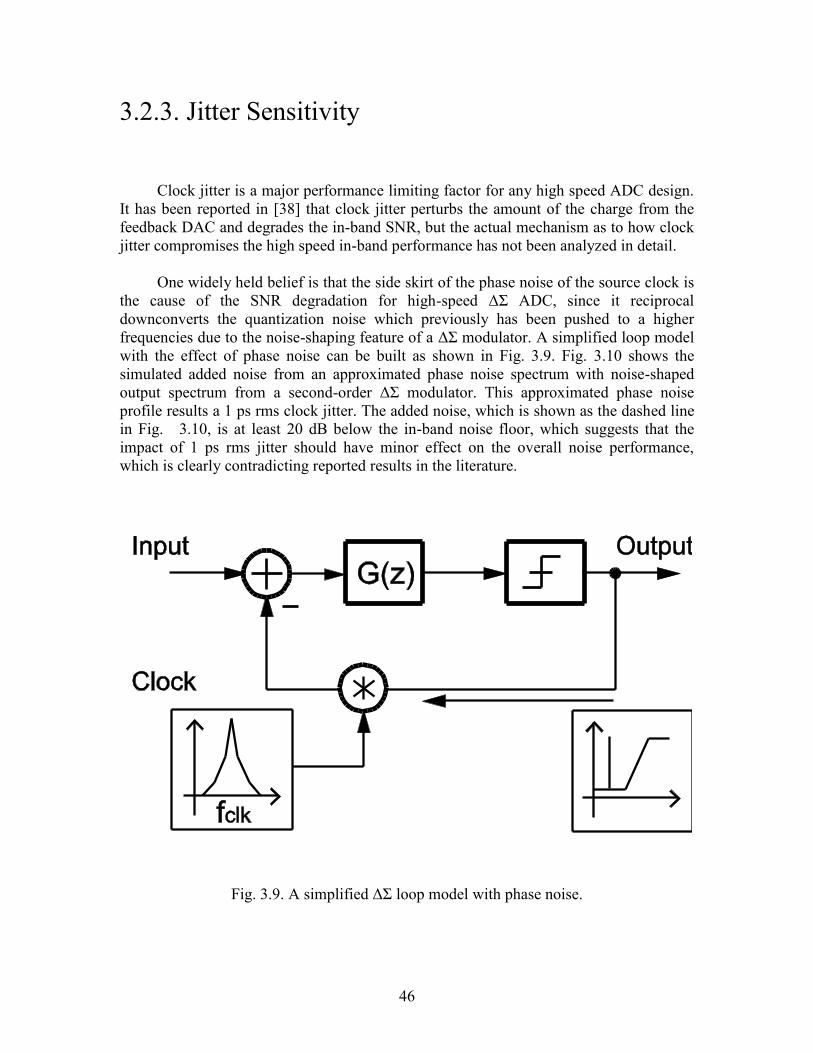
46
3.2.3. Jitter Sensitivity
Clock jitter is a major performance limiting factor for any high speed ADC design.
It has been reported in [38] that clock jitter perturbs the amount of the charge from the
feedback DAC and degrades the in-band SNR, but the actual mechanism as to how clock
jitter compromises the high speed in-band performance has not been analyzed in detail.
One widely held belief is that the side skirt of the phase noise of the source clock is
the cause of the SNR degradation for high-speed ΔΣ ADC, since it reciprocal
downconverts the quantization noise which previously has been pushed to a higher
frequencies due to the noise-shaping feature of a ΔΣ modulator. A simplified loop model
with the effect of phase noise can be built as shown in Fig. 3.9. Fig. 3.10 shows the
simulated added noise from an approximated phase noise spectrum with noise-shaped
output spectrum from a second-order ΔΣ modulator. This approximated phase noise
profile results a 1 ps rms clock jitter. The added noise, which is shown as the dashed line
in Fig. 3.10, is at least 20 dB below the in-band noise floor, which suggests that the
impact of 1 ps rms jitter should have minor effect on the overall noise performance,
which is clearly contradicting reported results in the literature.
Fig. 3.9. A simplified ΔΣ loop model with phase noise.

47
The physical origin of the jitter sensitivity of high-speed systems is the nonlinear
nature of the loop. A ΔΣ modulator can provide a dynamic range far exceeding the limit
of its low-resolution quantizer. In the time domain, the ΔΣ’s output is a pulse-density-
modulated (PDM) bit sequence as shown in Fig. 3.11. The PDM nature of the bit
sequence provides an additional dimension to encode data, so a ΔΣ ADC’s dynamic
range is not limited by its quantizer. When lower resolution is designated for the
quantizer, the modulator has to modulate the output density more aggressively to
maintain the same dynamic range compared to the case when the quanziter has higher
resolution. This result is more frequent switching between different levels in the output
sequence.
Fig. 3.10. Simulated output spectrum with phase noise model.
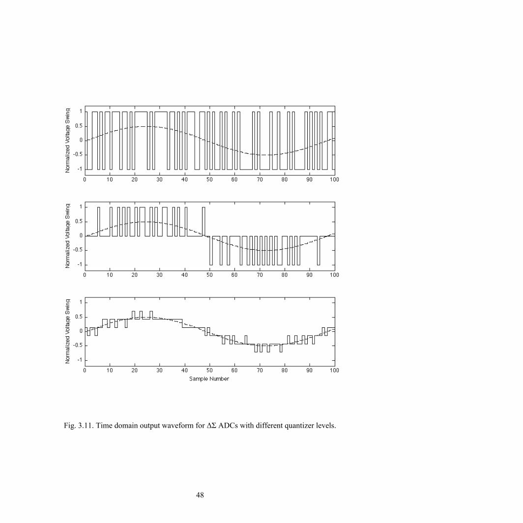
48
Fig. 3.11. Time domain output waveform for ΔΣ ADCs with different quantizer levels.
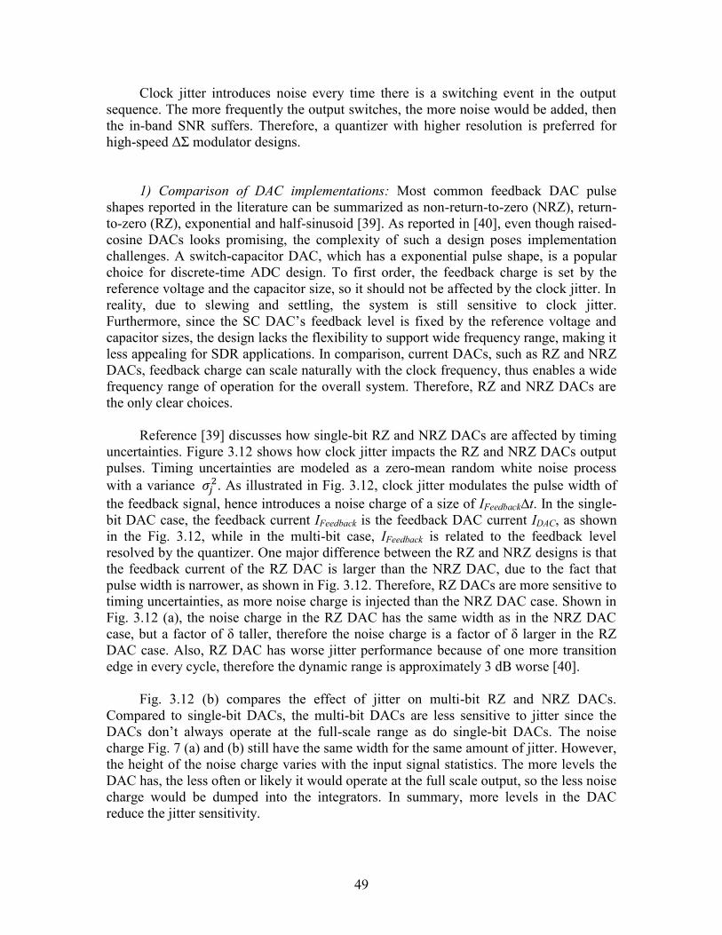
49
Clock jitter introduces noise every time there is a switching event in the output
sequence. The more frequently the output switches, the more noise would be added, then
the in-band SNR suffers. Therefore, a quantizer with higher resolution is preferred for
high-speed ΔΣ modulator designs.
1) Comparison of DAC implementations: Most common feedback DAC pulse
shapes reported in the literature can be summarized as non-return-to-zero (NRZ), return-
to-zero (RZ), exponential and half-sinusoid [39]. As reported in [40], even though raised-
cosine DACs looks promising, the complexity of such a design poses implementation
challenges. A switch-capacitor DAC, which has a exponential pulse shape, is a popular
choice for discrete-time ADC design. To first order, the feedback charge is set by the
reference voltage and the capacitor size, so it should not be affected by the clock jitter. In
reality, due to slewing and settling, the system is still sensitive to clock jitter.
Furthermore, since the SC DAC’s feedback level is fixed by the reference voltage and
capacitor sizes, the design lacks the flexibility to support wide frequency range, making it
less appealing for SDR applications. In comparison, current DACs, such as RZ and NRZ
DACs, feedback charge can scale naturally with the clock frequency, thus enables a wide
frequency range of operation for the overall system. Therefore, RZ and NRZ DACs are
the only clear choices.
Reference [39] discusses how single-bit RZ and NRZ DACs are affected by timing
uncertainties. Figure 3.12 shows how clock jitter impacts the RZ and NRZ DACs output
pulses. Timing uncertainties are modeled as a zero-mean random white noise process
with a variance . As illustrated in Fig. 3.12, clock jitter modulates the pulse width of
the feedback signal, hence introduces a noise charge of a size of IFeedback∆t. In the single-
bit DAC case, the feedback current IFeedback is the feedback DAC current IDAC, as shown
in the Fig. 3.12, while in the multi-bit case, IFeedback is related to the feedback level
resolved by the quantizer. One major difference between the RZ and NRZ designs is that
the feedback current of the RZ DAC is larger than the NRZ DAC, due to the fact that
pulse width is narrower, as shown in Fig. 3.12. Therefore, RZ DACs are more sensitive to
timing uncertainties, as more noise charge is injected than the NRZ DAC case. Shown in
Fig. 3.12 (a), the noise charge in the RZ DAC has the same width as in the NRZ DAC
case, but a factor of δ taller, therefore the noise charge is a factor of δ larger in the RZ
DAC case. Also, RZ DAC has worse jitter performance because of one more transition
edge in every cycle, therefore the dynamic range is approximately 3 dB worse [40].
Fig. 3.12 (b) compares the effect of jitter on multi-bit RZ and NRZ DACs.
Compared to single-bit DACs, the multi-bit DACs are less sensitive to jitter since the
DACs don’t always operate at the full-scale range as do single-bit DACs. The noise
charge Fig. 7 (a) and (b) still have the same width for the same amount of jitter. However,
the height of the noise charge varies with the input signal statistics. The more levels the
DAC has, the less often or likely it would operate at the full scale output, so the less noise
charge would be dumped into the integrators. In summary, more levels in the DAC
reduce the jitter sensitivity.
50
Fig. 3.12. Comparison of jitter impact on RZ and NRZ DACs.
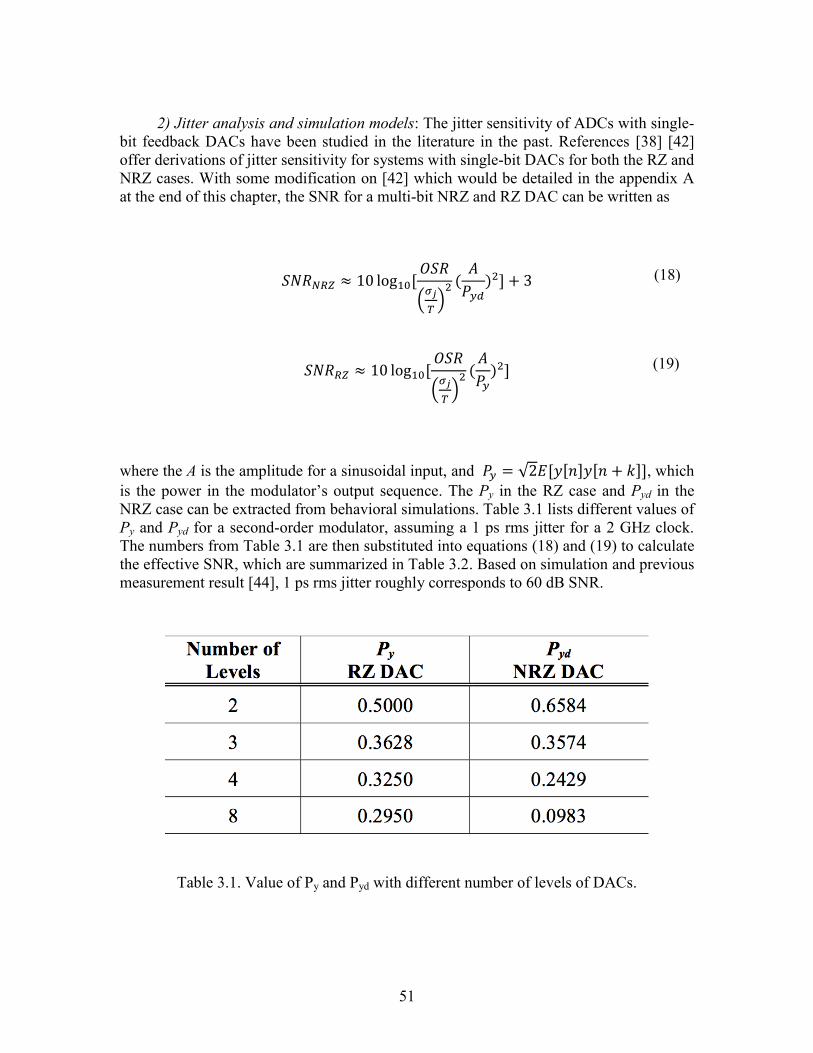
51
2) Jitter analysis and simulation models: The jitter sensitivity of ADCs with single-
bit feedback DACs have been studied in the literature in the past. References [38] [42]
offer derivations of jitter sensitivity for systems with single-bit DACs for both the RZ and
NRZ cases. With some modification on [42] which would be detailed in the appendix A
at the end of this chapter, the SNR for a multi-bit NRZ and RZ DAC can be written as
(
)
(
)
where the A is the amplitude for a sinusoidal input, and √ , which
is the power in the modulator’s output sequence. The Py in the RZ case and Pyd in the
NRZ case can be extracted from behavioral simulations. Table 3.1 lists different values of
Py and Pyd for a second-order modulator, assuming a 1 ps rms jitter for a 2 GHz clock.
The numbers from Table 3.1 are then substituted into equations (18) and (19) to calculate
the effective SNR, which are summarized in Table 3.2. Based on simulation and previous
measurement result [44], 1 ps rms jitter roughly corresponds to 60 dB SNR.
Table 3.1. Value of Py and Pyd with different number of levels of DACs.
(18)
(19)
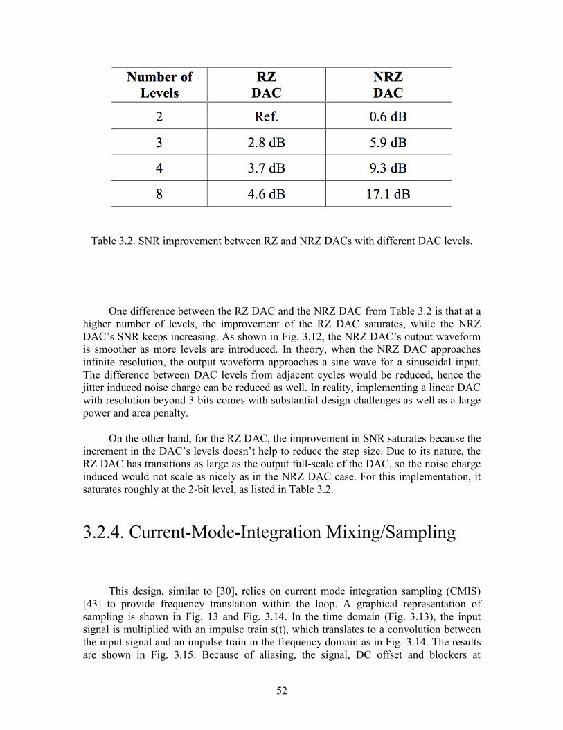
52
One difference between the RZ DAC and the NRZ DAC from Table 3.2 is that at a
higher number of levels, the improvement of the RZ DAC saturates, while the NRZ
DAC’s SNR keeps increasing. As shown in Fig. 3.12, the NRZ DAC’s output waveform
is smoother as more levels are introduced. In theory, when the NRZ DAC approaches
infinite resolution, the output waveform approaches a sine wave for a sinusoidal input.
The difference between DAC levels from adjacent cycles would be reduced, hence the
jitter induced noise charge can be reduced as well. In reality, implementing a linear DAC
with resolution beyond 3 bits comes with substantial design challenges as well as a large
power and area penalty.
On the other hand, for the RZ DAC, the improvement in SNR saturates because the
increment in the DAC’s levels doesn’t help to reduce the step size. Due to its nature, the
RZ DAC has transitions as large as the output full-scale of the DAC, so the noise charge
induced would not scale as nicely as in the NRZ DAC case. For this implementation, it
saturates roughly at the 2-bit level, as listed in Table 3.2.
3.2.4. Current-Mode-Integration Mixing/Sampling
This design, similar to [30], relies on current mode integration sampling (CMIS)
[43] to provide frequency translation within the loop. A graphical representation of
sampling is shown in Fig. 13 and Fig. 3.14. In the time domain (Fig. 3.13), the input
signal is multiplied with an impulse train s(t), which translates to a convolution between
the input signal and an impulse train in the frequency domain as in Fig. 3.14. The results
are shown in Fig. 3.15. Because of aliasing, the signal, DC offset and blockers at
Table 3.2. SNR improvement between RZ and NRZ DACs with different DAC levels.
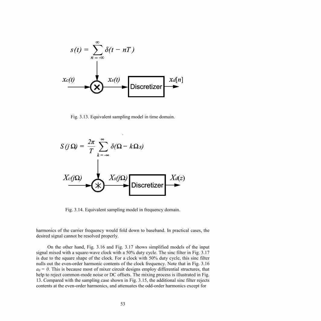
53
harmonics of the carrier frequency would fold down to baseband. In practical cases, the
desired signal cannot be resolved properly.
On the other hand, Fig. 3.16 and Fig. 3.17 shows simplified models of the input
signal mixed with a square-wave clock with a 50% duty cycle. The sinc filter in Fig. 3.17
is due to the square shape of the clock. For a clock with 50% duty cycle, this sinc filter
nulls out the even-order harmonic contents of the clock frequency. Note that in Fig. 3.16
a0 = 0. This is because most of mixer circuit designs employ differential structures, that
help to reject common-mode noise or DC offsets. The mixing process is illustrated in Fig.
13. Compared with the sampling case shown in Fig. 3.15, the additional sinc filter rejects
contents at the even-order harmonics, and attenuates the odd-order harmonics except for
Fig. 3.13. Equivalent sampling model in time domain.
.
Fig. 3.14. Equivalent sampling model in frequency domain.
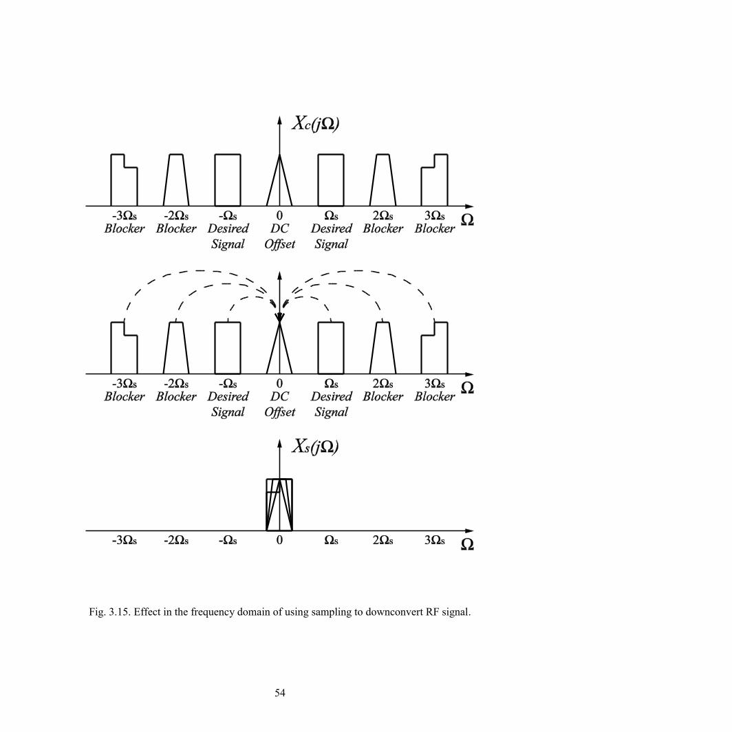
54
Fig. 3.15. Effect in the frequency domain of using sampling to downconvert RF signal.
.
55
the one at DC. It can be shown that the attenuation at is
, which is commonly
described as conversion loss in the RF-community. Fig. 3.18 also exposes that the
scheme is susceptible to higher order odd-order harmonics, such as the third-order
harmonic shown here, when mixing with a 50% duty-cycle clock.
Fig. 3.16. Equivalent mixing model in time domain.
.
Fig. 3.17. Equivalent mixing model in frequency domain.
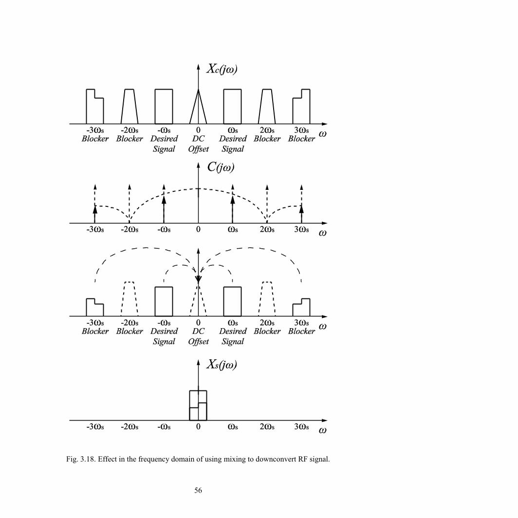
56
Fig. 3.18. Effect in the frequency domain of using mixing to downconvert RF signal.
.
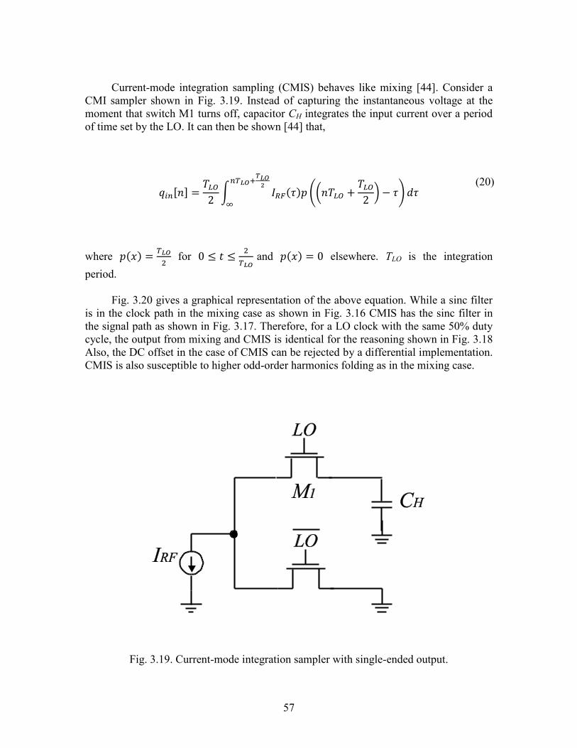
57
Current-mode integration sampling (CMIS) behaves like mixing [44]. Consider a
CMI sampler shown in Fig. 3.19. Instead of capturing the instantaneous voltage at the
moment that switch M1 turns off, capacitor CH integrates the input current over a period
of time set by the LO. It can then be shown [44] that,
∫ ((
) )
where
for
and elsewhere. TLO is the integration
period.
Fig. 3.20 gives a graphical representation of the above equation. While a sinc filter
is in the clock path in the mixing case as shown in Fig. 3.16 CMIS has the sinc filter in
the signal path as shown in Fig. 3.17. Therefore, for a LO clock with the same 50% duty
cycle, the output from mixing and CMIS is identical for the reasoning shown in Fig. 3.18
Also, the DC offset in the case of CMIS can be rejected by a differential implementation.
CMIS is also susceptible to higher odd-order harmonics folding as in the mixing case.
Fig. 3.19. Current-mode integration sampler with single-ended output.
(20)
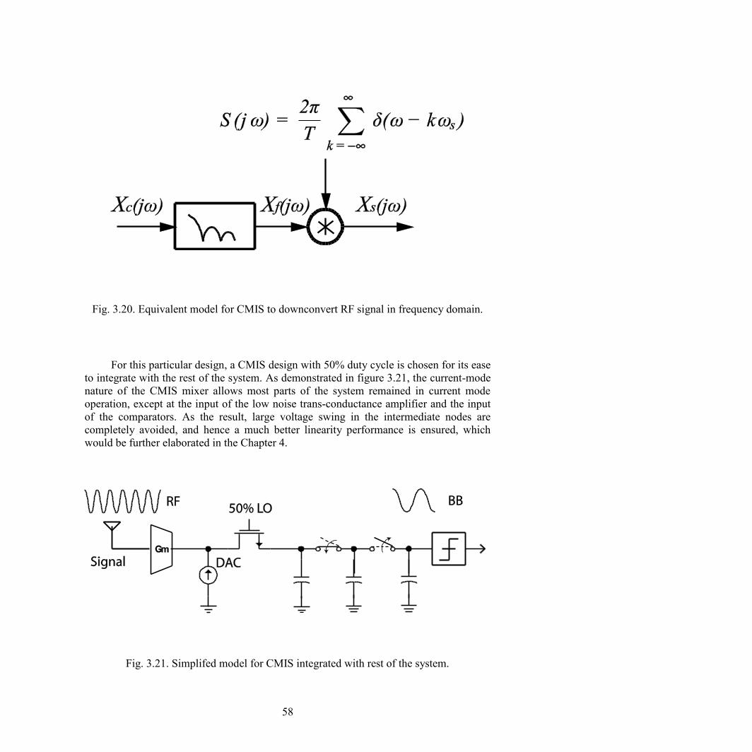
58
For this particular design, a CMIS design with 50% duty cycle is chosen for its ease
to integrate with the rest of the system. As demonstrated in figure 3.21, the current-mode
nature of the CMIS mixer allows most parts of the system remained in current mode
operation, except at the input of the low noise trans-conductance amplifier and the input
of the comparators. As the result, large voltage swing in the intermediate nodes are
completely avoided, and hence a much better linearity performance is ensured, which
would be further elaborated in the Chapter 4.
Fig. 3.21. Simplifed model for CMIS integrated with rest of the system.
Fig. 3.20. Equivalent model for CMIS to downconvert RF signal in frequency domain.
59
3.2.5. Summary
A four channel second-order ADC with CIFB all-feedback loop structure has been
chosen for this work in order to achieve a maximally flat STF response and flexibility to
support a wide frequency range. Also, a 2-bit NRZ DAC is selected for better jitter
immunity and lower power consumption compared to higher resolution options. Finally,
each of the ADCs is implemented as discrete-time as in [30] with a CMIS mixer
employed. The discrete-time design allows the CMIS mixers to be seamlessly integrated,
and helps to reduce the complexity for a system intended to operate over a wide range of
frequency.
60
Appendix A
Derivation OF Multi-Bit RZ and NRZ DAC Jitter
Sensitivity
The jitter sensitivity of ΔΣ ADCs with single-bit feedback DACs have been well
studied in the literature in the past. For this work, a modified derivation from [40] can
address the multi-bit feedback case. For any ΔΣ system in the jitter-free case, it is can be
shown as
Yo(z) is the output free from jitter, and X(z) is the input. Qo(z) is the quantization noise.
HNTF and HSTF stand for the noise transfer function and the signal transfer function.
With the impact of the clock jitter, the above equation can be rewritten as
where is the feedback signal modulated by the jitter, and Y(z) and Q(z) stands for
the output and the quantization noise with the effect of the clock jitter.
To extract the overall effect of the jitter,
(21)
(22)
(23)
61
where is the jitter-induced additional quantization noise. Within the low frequency
in-band, is suppressed by the huge loop gain from the noise transfer function,
therefore, its effect can be neglected. Therefore the above equation simplifies into
From (24), the output jitter-induced noise PSD can be described as
| |
is the discrete-time Fourier transform (DTFT) of the autocorrelation of .
Given the fact that the clock jitter is uncorrelated with the quantized output, then
where . j[n] is the small perturbation around the ideal
clock edge induced by the jitter. Let , then , therefore,
where Pyd is the autocorrelation between different yd[n]. Pyd is the key in describing a ΔΣ
modulator’s performance under the impact of the clock jitter. From the early discussion,
it has been shown that the performance under the jitter is related to the loop dynamic,
input signal statistic and the system’s nonlinear nature. Pyd helps to capture all of these
essential pieces of information for the jitter analysis of a ΔΣ system.
From (25) and (27), the jitter-induced in-band noise PSD is
| |
(24)
(25)
(26)
(27)
(28)
62
Following the analysis shown in the appendix in [42], near the center of the
passband, the signal transfer function can be expressed as
| |
|
|
Since the interest here is the low-frequency in-band, the
.
Therefore, the overall in-band jitter-induced noise power is then given by
Equation (30) suggests that the clock jitter is not noise shaped but simply spreading
by OSR, due to the fact that the jitter is injected through the first DAC. The loop filter
would treat it in the same way as it does to the input signal, therefore, the jitter noise is
not noise shaped. Finally, the SNR of a ΔΣ modulator with a multi-bit NRZ DAC with a
sinusoidal input with amplitude A can be shown as
(
)
For the RZ DAC case, equation (27) can be rewritten as
where √ , which is the power in the modulator’s output sequence.
And the rest of the analysis will follow what has been shown above. Then
(
)
(29)
(30)
(31)
(32)
(33)
63
Chapter 4
Experimental Prototype
4.1. Introduction to System Implementation
The overall architecture of the receiver is shown in Fig. 4.1. For the sake of clarity,
the system diagram is shown as single-ended, while the actual design is fully differential.
The ΔΣ receiver includes both I and Q channels. A low noise transconducatance amplifier
(LNTA) in each channel converts the input RF voltage into an output RF current. A
programmable gain of 20 dB is implemented by changing the bias current in both the
LNTA and the feedback DACs. As shown in Fig. 4.1, the output of the LNTA is then
split into two interleaved paths for I and Q channels, each of which contains a pair of
passive mixers, which are implemented as a pair of CMIS switches, The signal is then
processed by a second-order loop filter implemented using a passive switched-capacitor
network. A two-bit quantizer is digitizing the filtered signal and its output is fed back to
the RF summing node.
With two channels of ΔΣ ADC’s RF feedback signal, an effective bandpass
feedback is created at the summing node. This multi-bit bandpass feedback suppresses
the RF voltage swing; consequently, it improves the overall linearity performance. In
comparison to [31][30], the two-bit network effectively reduces the swing at RF node by
a factor of three. However, due to the lack of front-end gain, the reduced swing in the
system posed a serious design challenge on the comparator design, which will be
thoroughly discussed in this section. The entire system takes in an external clock
operating at twice the speed of the carrier frequency. All the necessary clock phases
needed are then generated internally.
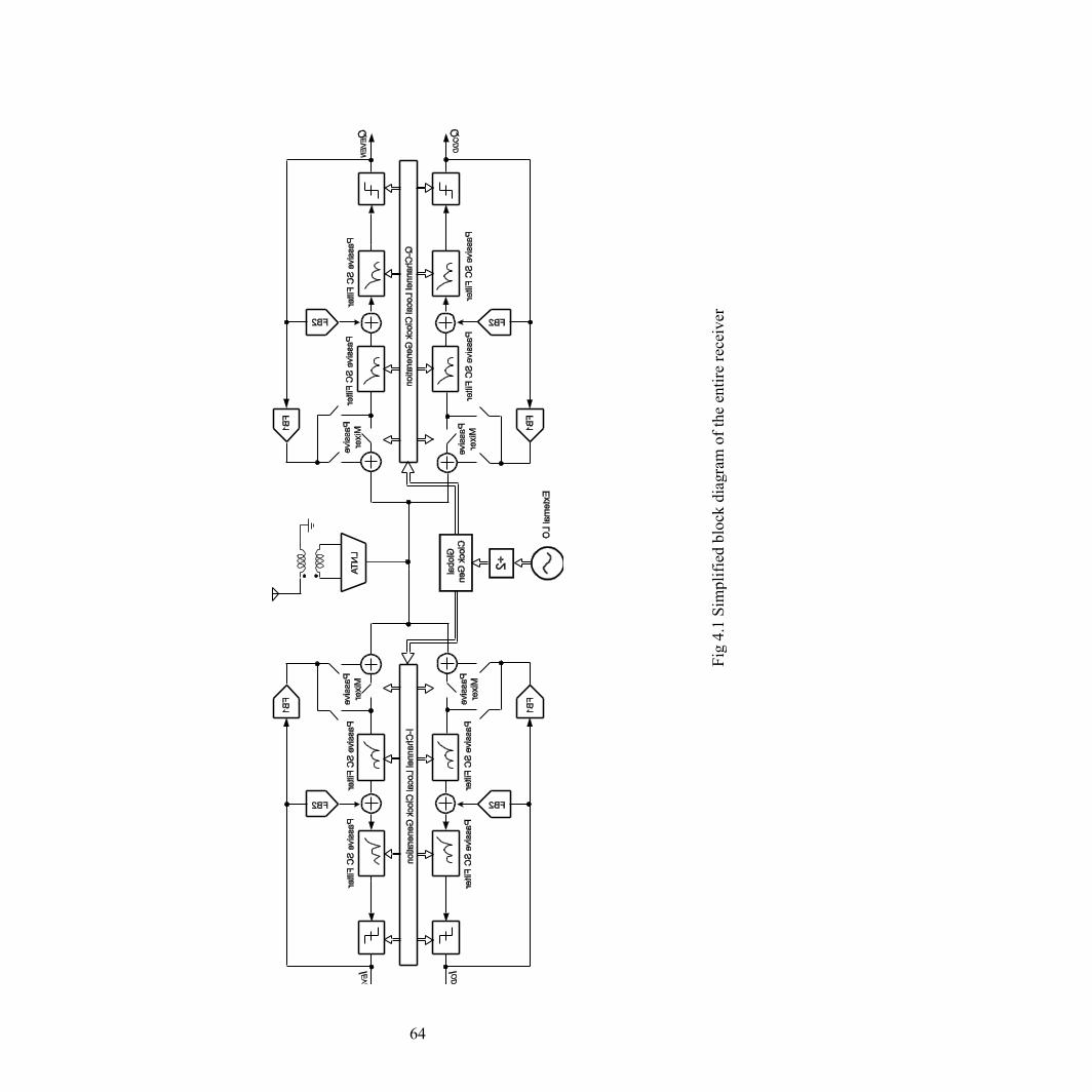
64
Fig
4.1
Sim
pli
fied
blo
ck d
iagra
m o
f th
e en
tire
rec
eiver
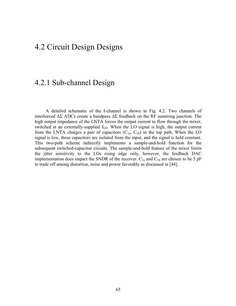
65
4.2 Circuit Design Designs
4.2.1 Sub-channel Design
A detailed schematic of the I-channel is shown in Fig. 4.2. Two channels of
interleaved ΔΣ ADCs create a bandpass ΔΣ feedback on the RF summing junction. The
high output impedance of the LNTA forces the output current to flow through the mixer,
switched at an externally-supplied fLO. When the LO signal is high, the output current
from the LNTA charges a pair of capacitors (C1a, C1b) in the top path. When the LO
signal is low, these capacitors are isolated from the input, and the signal is held constant.
This two-path scheme indirectly implements a sample-and-hold function for the
subsequent switched-capacitor circuits. The sample-and-hold feature of the mixer limits
the jitter sensitivity to the LOs rising edge only, however, the feedback DAC
implementation does impact the SNDR of the receiver. C1a and C1b are chosen to be 5 pF
to trade off among distortion, noise and power favorably as discussed in [44].
66
Fig. 4.2. Simplified schematic of the I-channel.
.

67
4.2.2 Low Noise Transconductance Amplifier
Fig. 4.3 illustrates the design of the front-end LNTA. A class-AB dual common
gate (CG) amplifier provides both wide-band input matching and good linearity. To
improve both noise performance and power efficiency, the gm of the four tail current
sources are reused by AC-coupling the RF input signal to their respective gates. The
input common-mode voltage is set by two replica biases that mimic the biasing
conditions of the NMOS CG and the PMOS CG. The LNTAs differential outputs are AC-
coupled to the mixer switches, and the output common mode voltage is set by a common-
mode feedback amplifier connected to the mixers. The LNTA provides a
transconductance gain of up to 20 dB from a 1.5 V supply with the CMIS circuits. The
key feature is that the entire system is based on current mode operation. All the internal
nodes are at low impedance (enforced by the cascode devices) except for the output
nodes, whose swing is suppressed by the low impedance enforced by the global loop.
One major issue with such a design is how to combine the output current. Since
there are two pairs of output currents flowing out of the LNTA, no conventional
techniques can be used. One possibility is to borrow the idea of distributive active
transformer (DAT) from [16] to create an active transformer current summation network
as shown in Fig. 4.4. One nice benefit of transformer-based output combining network is
that the transformer network itself, with proper design, can absorb the parasitic capacitor
loadings on each side, therefore, it can potentially achieve a low-loss signal combining.
Moreover, the common-mode voltage can be easily defined by connecting a desired bias
voltage to the center tap on the secondary winding. However, software-define radio
system need to operate at a low frequency range, where the transformer design could cost
a huge area overhead. In addition, because of the insertion loss requirement, a
transformer network could only support a rather limited frequency range. This makes
transformer-based design less appealing for software define radio application, where a
wide range of frequency of operation is a must. The transformer structure shown in Fig.
4.4 has a size of 200 μm by 200 μm. It can only support a tunable range up to 500 MHz
centering around 2 GHz, which is clearly not enough for software-define radio
application.
As the result, a capacitor-coupling network is used. To carefully manage the
insertion loss, different capacitor layout structures have been studied. Iterations on
different layout structures and their extraction results have suggested that avoiding the
first and second layers of metal provides the best tradeoff between area overhead and the
overall insertion loss. Detail analysis results are listed in Table 4.1. The extracted
parasitic capacitor results are also further verified with the aid of 3D simulation cad tools
such as EMX, which is also listed in Table 4.1.
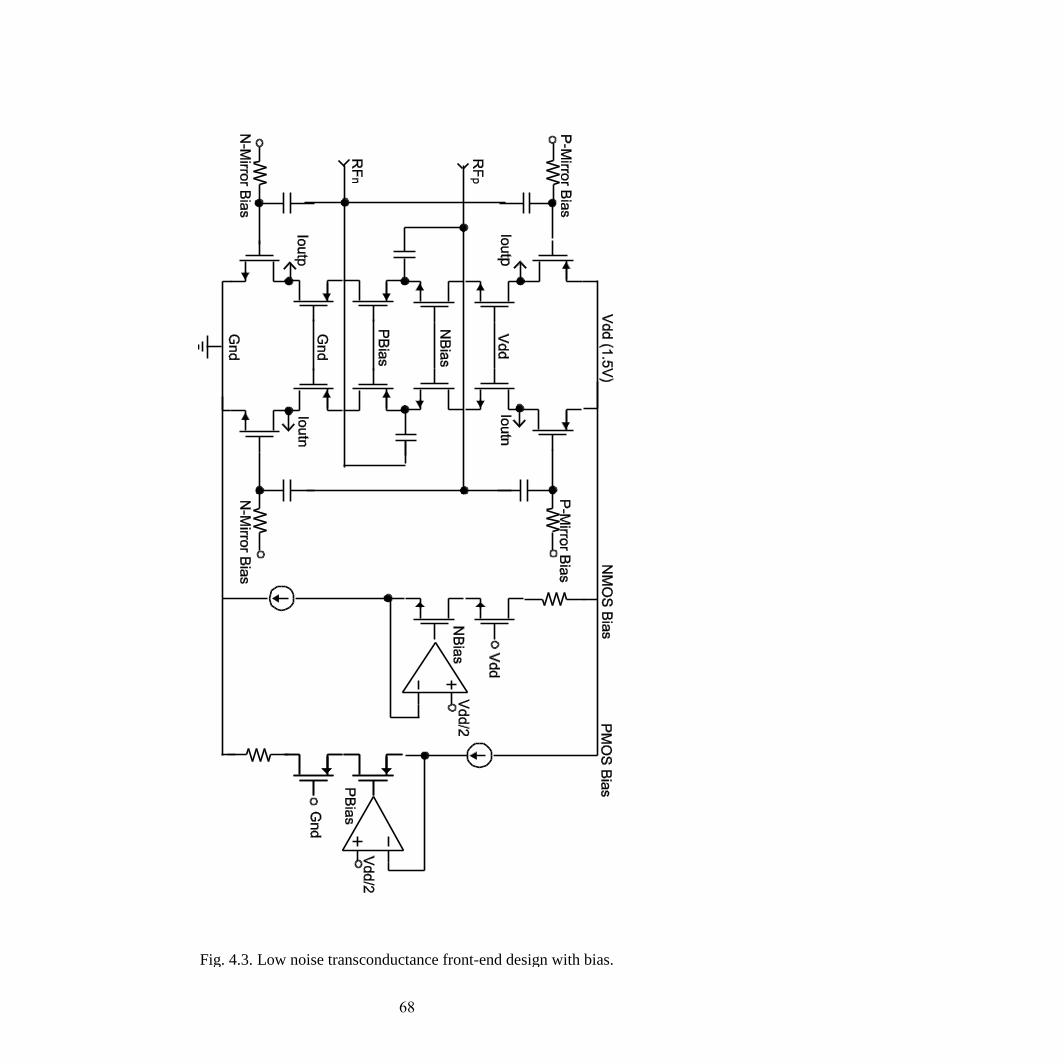
68
Fig. 4.3. Low noise transconductance front-end design with bias.
.
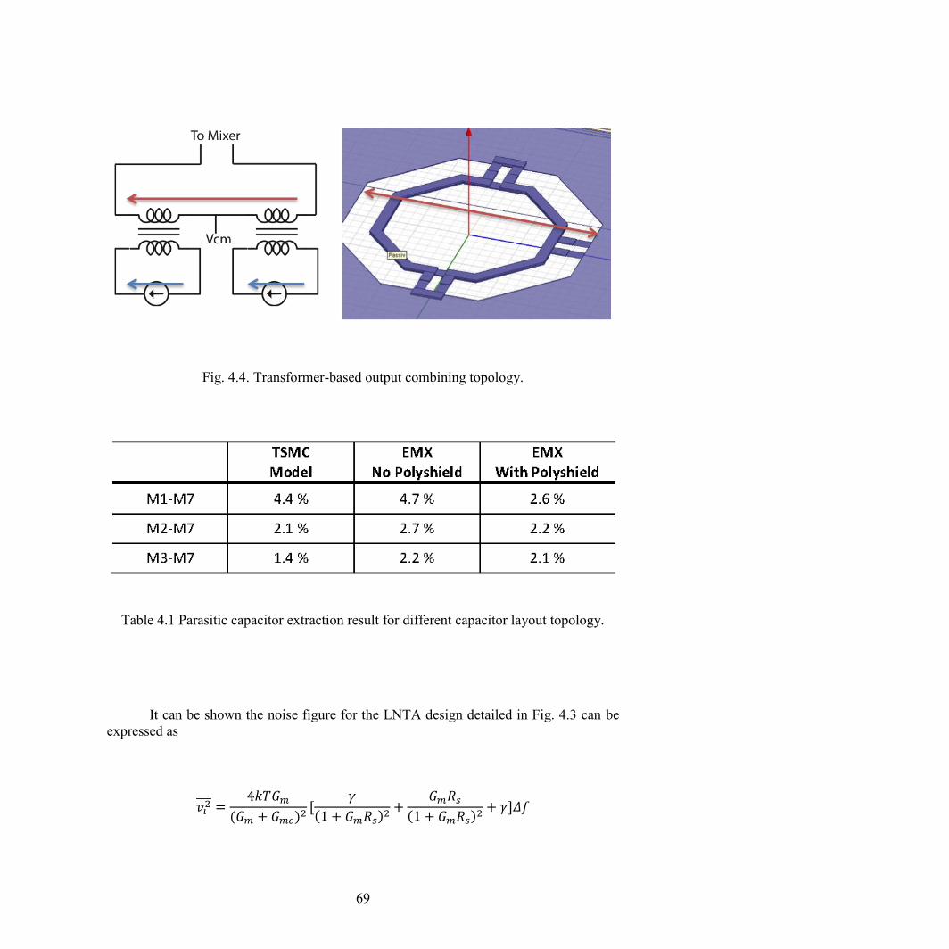
69
It can be shown the noise figure for the LNTA design detailed in Fig. 4.3 can be
expressed as
Fig. 4.4. Transformer-based output combining topology.
Table 4.1 Parasitic capacitor extraction result for different capacitor layout topology.

70
where Gm = gmn + gmp is the overall trans-conductance of the common-source stages, and
Gmc = gmnc + gmpc is the overall trans-conductance for the common gate stages. Rs stands
for the loading impedance presented from the next stage.
Fig. 4.5. 3-dimentional NF plot and 2-dimentional NF contour.
(34)
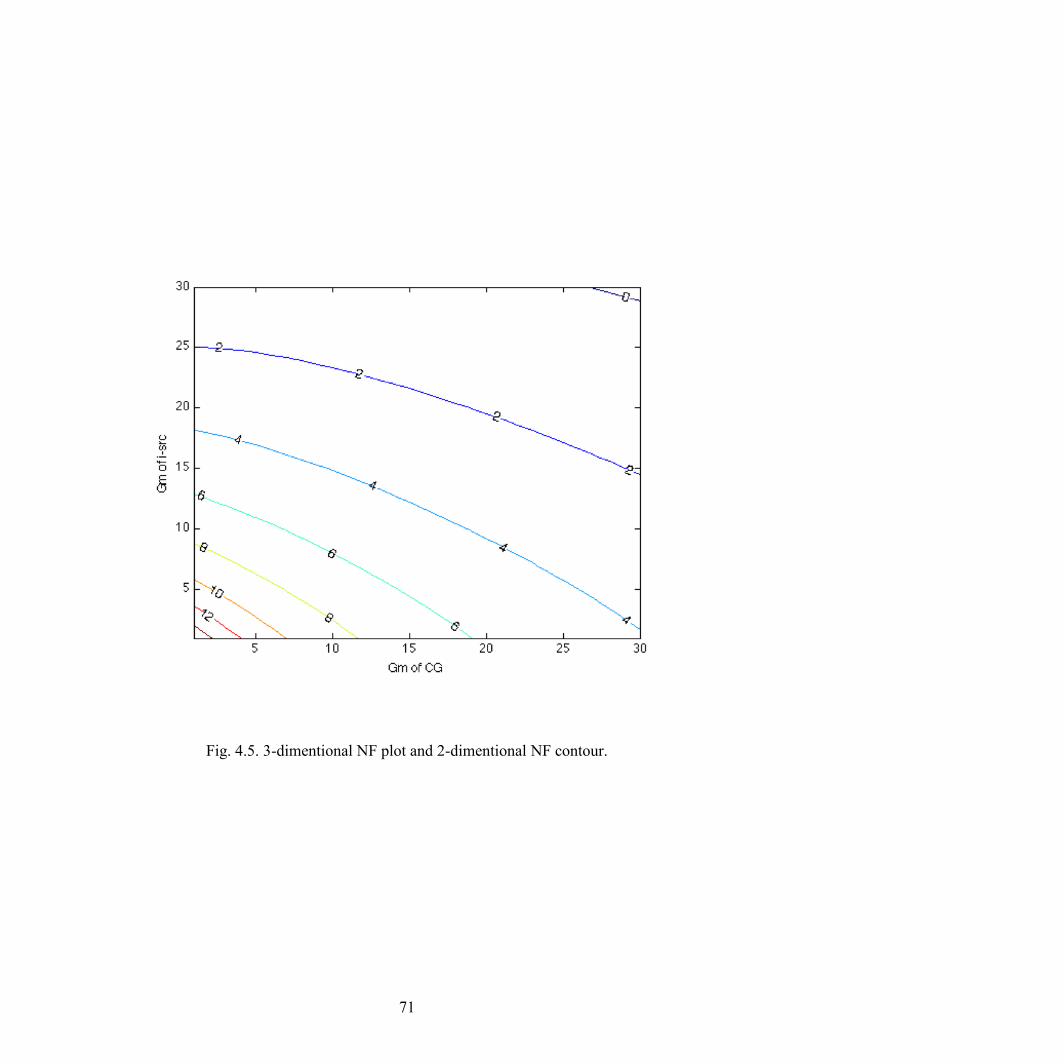
71
Fig. 4.5. 3-dimentional NF plot and 2-dimentional NF contour.
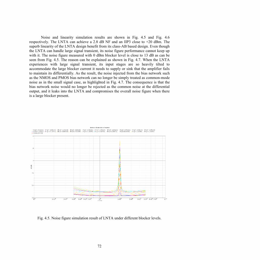
72
Noise and linearity simulation results are shown in Fig. 4.5 and Fig. 4.6
respectively. The LNTA can achieve a 2.8 dB NF and an IIP3 close to +20 dBm. The
superb linearity of the LNTA design benefit from its class-AB based design. Even though
the LNTA can handle large signal transient, its noise figure performance cannot keep up
with it. The noise figure measured with 0 dBm blocker level is close to 13 dB as can be
seen from Fig. 4.5. The reason can be explained as shown in Fig. 4.7. When the LNTA
experiences with large signal transient, its input stages are so heavily tilted to
accommodate the large blocker current it needs to supply or sink that the amplifier fails
to maintain its differentially. As the result, the noise injected from the bias network such
as the NMOS and PMOS bias network can no longer be simply treated as common-mode
noise as in the small signal case, as highlighted in Fig. 4.7. The consequence is that the
bias network noise would no longer be rejected as the common noise at the differential
output, and it leaks into the LNTA and compromises the overall noise figure when there
is a large blocker present.
Fig. 4.5. Noise figure simulation result of LNTA under different blocker levels.
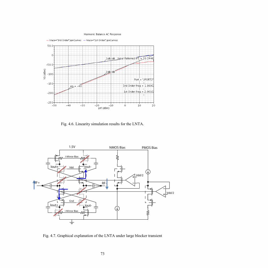
73
Fig. 4.6. Linearity simulation results for the LNTA.
Fig. 4.7. Graphical explanation of the LNTA under large blocker transient
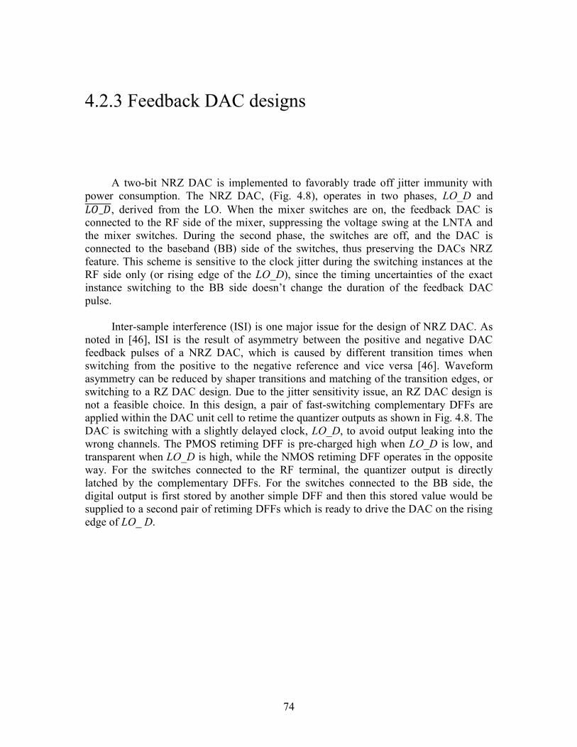
74
4.2.3 Feedback DAC designs
A two-bit NRZ DAC is implemented to favorably trade off jitter immunity with
power consumption. The NRZ DAC, (Fig. 4.8), operates in two phases, LO_D and
, derived from the LO. When the mixer switches are on, the feedback DAC is
connected to the RF side of the mixer, suppressing the voltage swing at the LNTA and
the mixer switches. During the second phase, the switches are off, and the DAC is
connected to the baseband (BB) side of the switches, thus preserving the DACs NRZ
feature. This scheme is sensitive to the clock jitter during the switching instances at the
RF side only (or rising edge of the LO_D), since the timing uncertainties of the exact
instance switching to the BB side doesn’t change the duration of the feedback DAC
pulse.
Inter-sample interference (ISI) is one major issue for the design of NRZ DAC. As
noted in [46], ISI is the result of asymmetry between the positive and negative DAC
feedback pulses of a NRZ DAC, which is caused by different transition times when
switching from the positive to the negative reference and vice versa [46]. Waveform
asymmetry can be reduced by shaper transitions and matching of the transition edges, or
switching to a RZ DAC design. Due to the jitter sensitivity issue, an RZ DAC design is
not a feasible choice. In this design, a pair of fast-switching complementary DFFs are
applied within the DAC unit cell to retime the quantizer outputs as shown in Fig. 4.8. The
DAC is switching with a slightly delayed clock, LO_D, to avoid output leaking into the
wrong channels. The PMOS retiming DFF is pre-charged high when LO_D is low, and
transparent when LO_D is high, while the NMOS retiming DFF operates in the opposite
way. For the switches connected to the RF terminal, the quantizer output is directly
latched by the complementary DFFs. For the switches connected to the BB side, the
digital output is first stored by another simple DFF and then this stored value would be
supplied to a second pair of retiming DFFs which is ready to drive the DAC on the rising
edge of LO_ D.
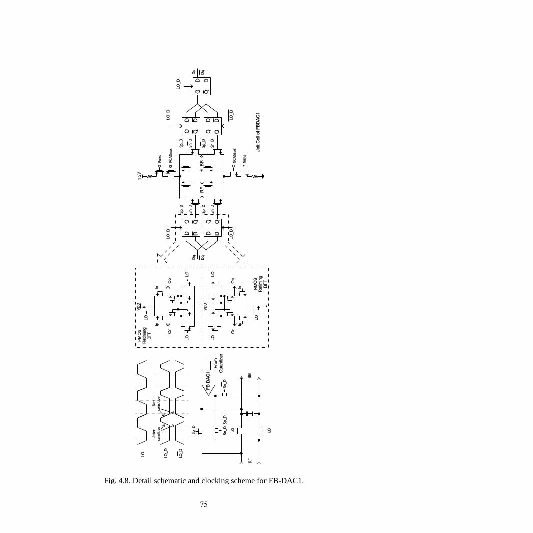
75
Fig. 4.8. Detail schematic and clocking scheme for FB-DAC1.
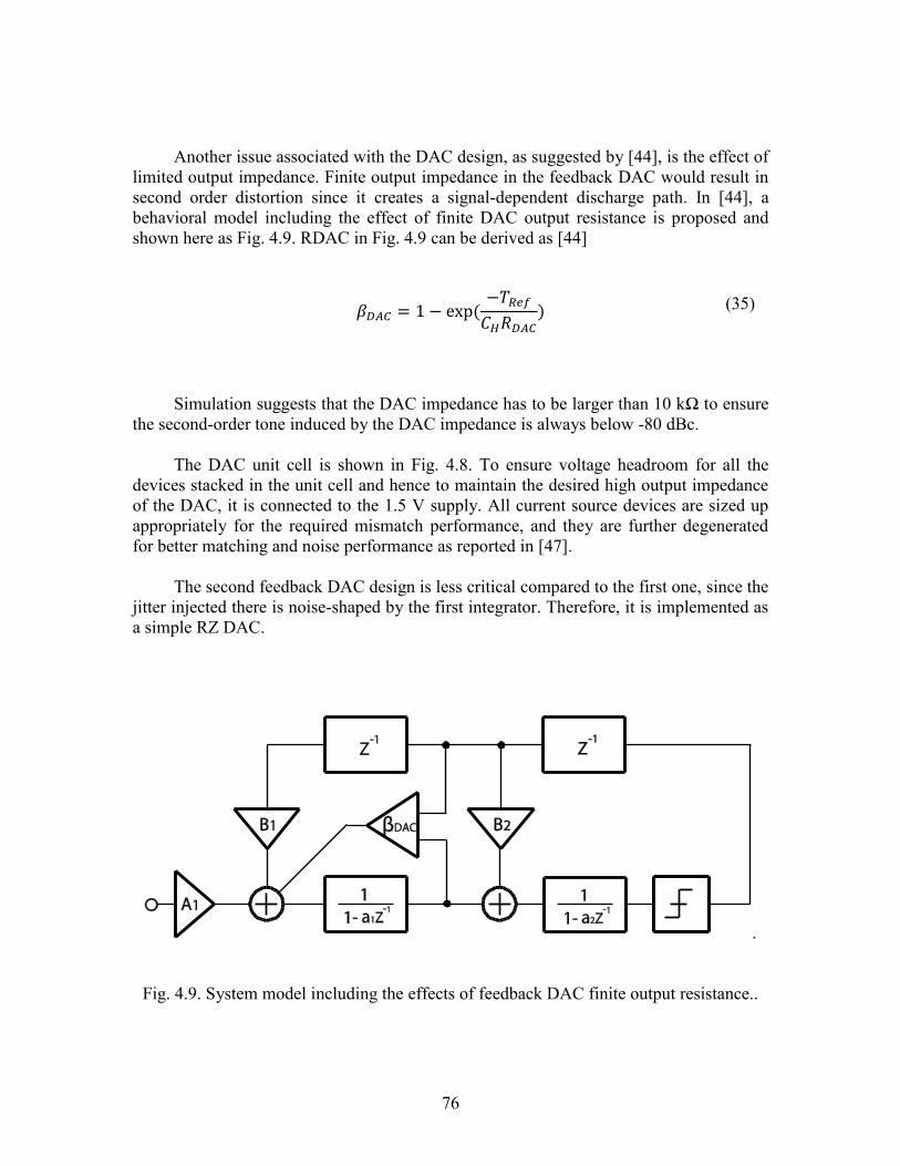
76
Another issue associated with the DAC design, as suggested by [44], is the effect of
limited output impedance. Finite output impedance in the feedback DAC would result in
second order distortion since it creates a signal-dependent discharge path. In [44], a
behavioral model including the effect of finite DAC output resistance is proposed and
shown here as Fig. 4.9. RDAC in Fig. 4.9 can be derived as [44]
Simulation suggests that the DAC impedance has to be larger than 10 kΩ to ensure
the second-order tone induced by the DAC impedance is always below -80 dBc.
The DAC unit cell is shown in Fig. 4.8. To ensure voltage headroom for all the
devices stacked in the unit cell and hence to maintain the desired high output impedance
of the DAC, it is connected to the 1.5 V supply. All current source devices are sized up
appropriately for the required mismatch performance, and they are further degenerated
for better matching and noise performance as reported in [47].
The second feedback DAC design is less critical compared to the first one, since the
jitter injected there is noise-shaped by the first integrator. Therefore, it is implemented as
a simple RZ DAC.
.
Fig. 4.9. System model including the effects of feedback DAC finite output resistance..
(35)
77
4.2.4. Comparator Design
The comparator design is quite challenging due to the speed and precision
requirements. The comparator requires a short decision time (200 ps), a small input-
referred noise level (200 mV), and low power consumption (4 mW at 2 GHz). As shown
in Fig. 4.10, the comparator core is implemented using a calibrated pre-amplifier
followed by a sense-amplifier-based latch. The pre-amplifier helps to ease the stringent
input-referred noise and mismatch requirements (0.5 mV) posed on the comparator, due
to the lack of front-end gain in the system. The mismatch of the core comparators is
further suppressed through an integrated calibration DAC to avoid using excessively
large devices. To calibrate the mismatch, the comparators’ inputs are first disconnected
from the loop and tied to a on-chip reference ladder. Then, the optimum codes for each
comparator can be found by sweeping through the DAC. Finally, the comparators are
connected back to the loop. This is a one time process, and is robust over different
frequencies.
To reduce the jitter sensitivity, more feedback levels are preferable. However, it
also poses a more stringent requirement on the comparators’ mismatch performance. Fig.
4.11 compares the quantizer area with respect to the resolution in the quantizer. To meet
the mismatch requirement, the comparators need to be excessively large in conventional
design. With calibration, the quantizer can be four times smaller.
To better understand the area overhead of the calibrated quantizer, its area
breakdown is shown in Fig. 4.12. At the one bit level, the size of the decoder dominates.
At higher resolution, the area of the calibration DAC dominates. At the 2 bit level, the
decoder has a similar size as the calibration DAC. It is also worth noting that a 3-bit
quantizer has a size that is 10 times larger than a 2-bit quantizer, even with the
calibration. For the current design, the quantizer occupies around 10% of the overall area.
If a 3-bit design is adopted, the quantizer would have a comparable size to the current
system.
Another benefit with calibration is power saving as shown in Fig. 4.13. Without
calibration, each comparator cell scales up exponentially with resolution to meet the
stringent mismatch requirements. Meanwhile, more unit cells are needed. Hence, the
switching power increases more rapidly. With calibration, more cells are still needed, but
each cell stays the same size; only the size of the calibration DAC increases
exponentially. Therefore, power overhead is less severe than the un-calibrated case.
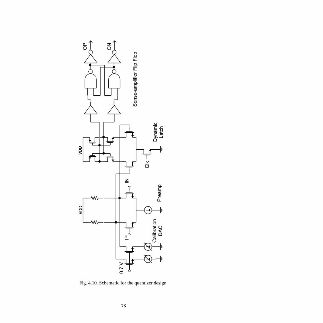
78
Fig. 4.10. Schematic for the quantizer design.
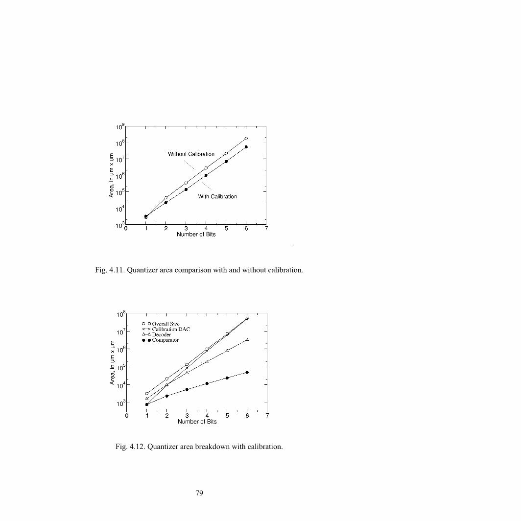
79
.
Fig. 4.11. Quantizer area comparison with and without calibration.
Fig. 4.12. Quantizer area breakdown with calibration.
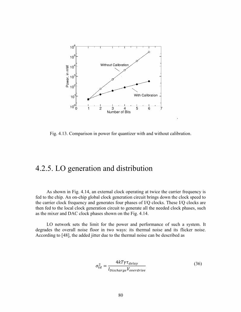
80
4.2.5. LO generation and distribution
As shown in Fig. 4.14, an external clock operating at twice the carrier frequency is
fed to the chip. An on-chip global clock generation circuit brings down the clock speed to
the carrier clock frequency and generates four phases of I/Q clocks. These I/Q clocks are
then fed to the local clock generation circuit to generate all the needed clock phases, such
as the mixer and DAC clock phases shown on the Fig. 4.14.
LO network sets the limit for the power and performance of such a system. It
degrades the overall noise floor in two ways: its thermal noise and its flicker noise.
According to [48], the added jitter due to the thermal noise can be described as
.
Fig. 4.13. Comparison in power for quantizer with and without calibration.
(36)
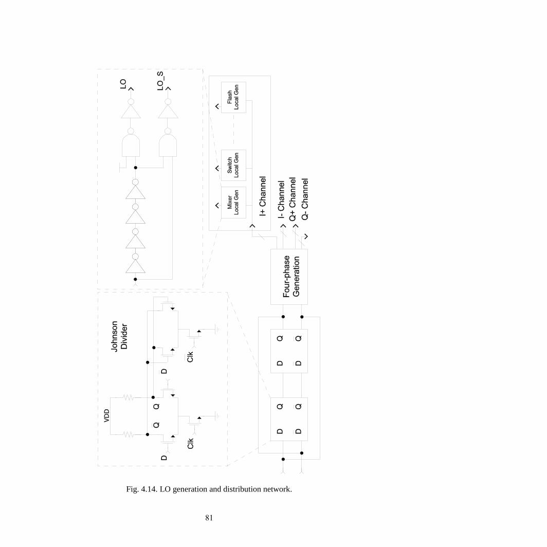
81
Fig. 4.14. LO generation and distribution network.

82
This suggests the added jitter can only be reduced by sizing up the discharge
current and reducing the delay time, which is just sizing up the devices. For short, sizing
up the devices would improve both its edge rate and its flicker noise performance, but it
comes with large power penalty. Noise simulations on the Mixer and the first feedback
DAC paths have revealed that the added jitter is 920 fs with 9 mW power consumption
under 2 GHz operation. The effect of the flicker noise will be later discussed in the next
section.
4.3. Measurement
The chip is implemented in TSMC’s 65nm GP technology. The chip
photomicrograph is shown in Fig. 4.15, highlighting that the receiver occupies an area of
850 m x 650 m, including the calibration DACs for the comparators as well as the local
bypass capacitance.
.
Fig. 4.15. Chip Microphotograph.
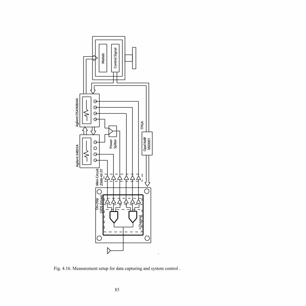
83
.
Fig. 4.16. Measurement setup for data capturing and system control .
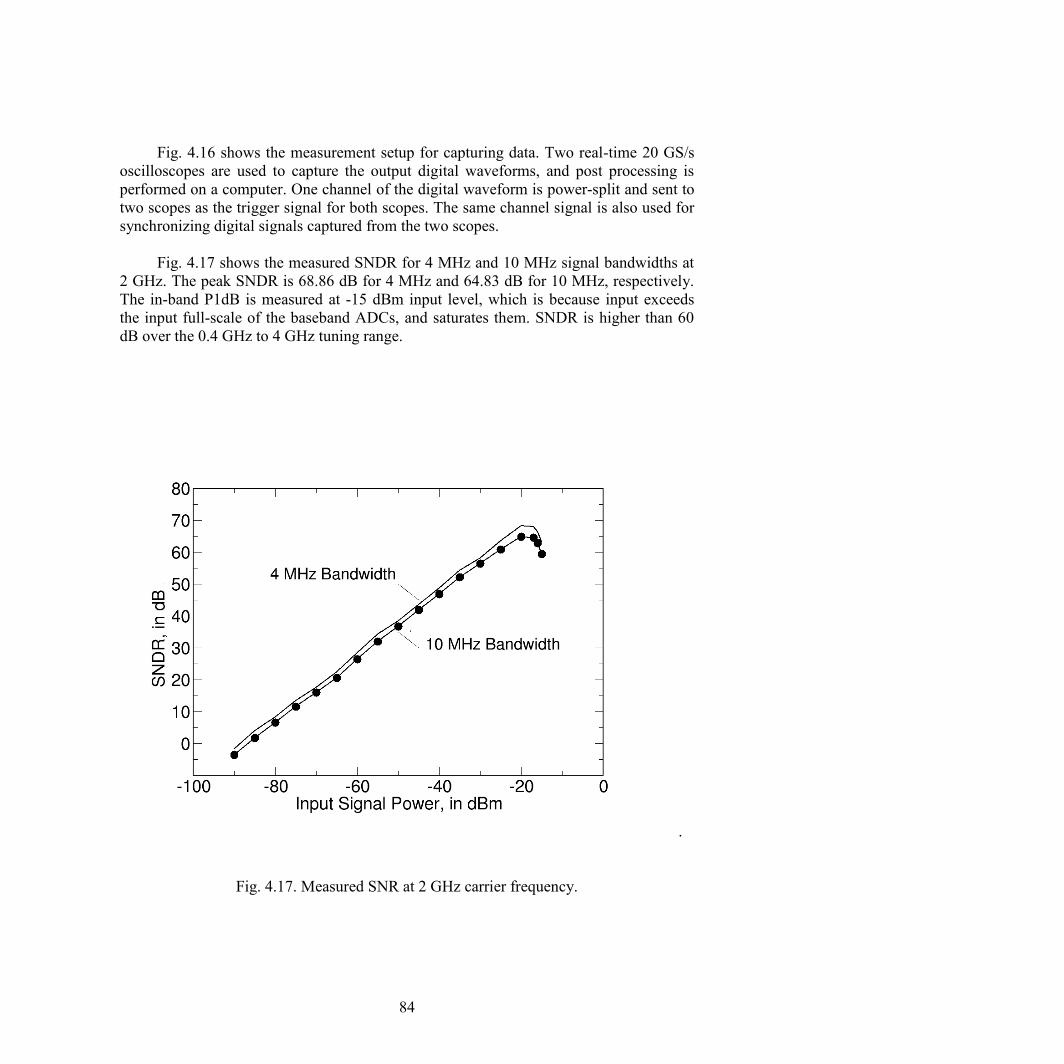
84
Fig. 4.16 shows the measurement setup for capturing data. Two real-time 20 GS/s
oscilloscopes are used to capture the output digital waveforms, and post processing is
performed on a computer. One channel of the digital waveform is power-split and sent to
two scopes as the trigger signal for both scopes. The same channel signal is also used for
synchronizing digital signals captured from the two scopes.
Fig. 4.17 shows the measured SNDR for 4 MHz and 10 MHz signal bandwidths at
2 GHz. The peak SNDR is 68.86 dB for 4 MHz and 64.83 dB for 10 MHz, respectively.
The in-band P1dB is measured at -15 dBm input level, which is because input exceeds
the input full-scale of the baseband ADCs, and saturates them. SNDR is higher than 60
dB over the 0.4 GHz to 4 GHz tuning range.
.
Fig. 4.17. Measured SNR at 2 GHz carrier frequency.
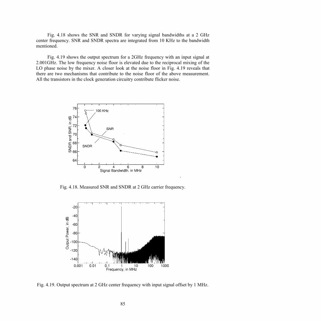
85
Fig. 4.18 shows the SNR and SNDR for varying signal bandwidths at a 2 GHz
center frequency. SNR and SNDR spectra are integrated from 10 KHz to the bandwidth
mentioned.
Fig. 4.19 shows the output spectrum for a 2GHz frequency with an input signal at
2.001GHz. The low frequency noise floor is elevated due to the reciprocal mixing of the
LO phase noise by the mixer. A closer look at the noise floor in Fig. 4.19 reveals that
there are two mechanisms that contribute to the noise floor of the above measurement.
All the transistors in the clock generation circuitry contribute flicker noise.
.
Fig. 4.18. Measured SNR and SNDR at 2 GHz carrier frequency.
Fig. 4.19. Output spectrum at 2 GHz center frequency with input signal offset by 1 MHz.
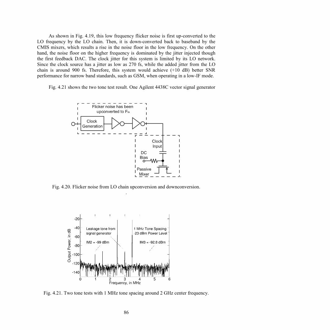
86
As shown in Fig. 4.19, this low frequency flicker noise is first up-converted to the
LO frequency by the LO chain. Then, it is down-converted back to baseband by the
CMIS mixers, which results a rise in the noise floor in the low frequency. On the other
hand, the noise floor on the higher frequency is dominated by the jitter injected though
the first feedback DAC. The clock jitter for this system is limited by its LO network.
Since the clock source has a jitter as low as 270 fs, while the added jitter from the LO
chain is around 900 fs. Therefore, this system would achieve (+10 dB) better SNR
performance for narrow band standards, such as GSM, when operating in a low-IF mode.
Fig. 4.21 shows the two tone test result. One Agilent 4438C vector signal generator
.
Fig. 4.20. Flicker noise from LO chain upconversion and downconversion.
.
Fig. 4.21. Two tone tests with 1 MHz tone spacing around 2 GHz center frequency.
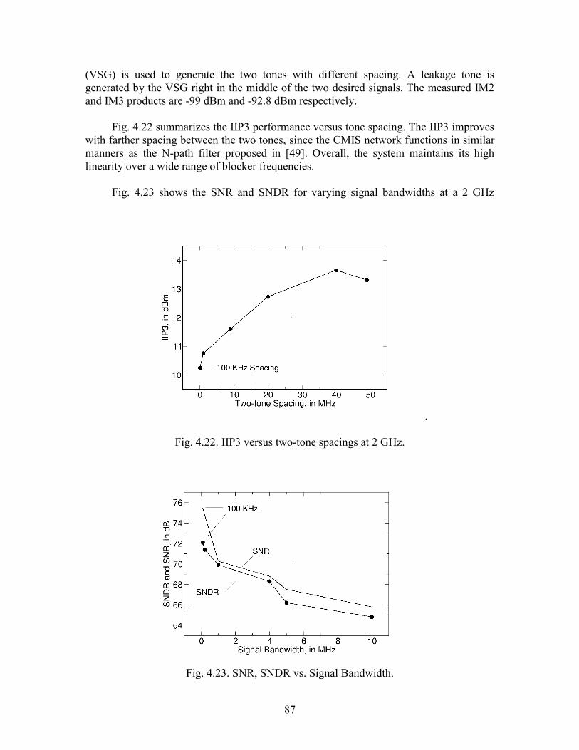
87
(VSG) is used to generate the two tones with different spacing. A leakage tone is
generated by the VSG right in the middle of the two desired signals. The measured IM2
and IM3 products are -99 dBm and -92.8 dBm respectively.
Fig. 4.22 summarizes the IIP3 performance versus tone spacing. The IIP3 improves
with farther spacing between the two tones, since the CMIS network functions in similar
manners as the N-path filter proposed in [49]. Overall, the system maintains its high
linearity over a wide range of blocker frequencies.
Fig. 4.23 shows the SNR and SNDR for varying signal bandwidths at a 2 GHz
.
Fig. 4.22. IIP3 versus two-tone spacings at 2 GHz.
Fig. 4.23. SNR, SNDR vs. Signal Bandwidth.
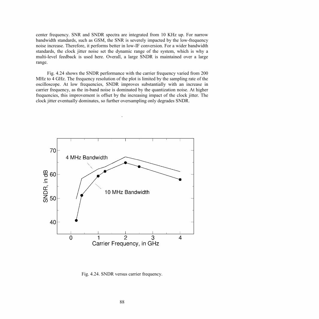
88
center frequency. SNR and SNDR spectra are integrated from 10 KHz up. For narrow
bandwidth standards, such as GSM, the SNR is severely impacted by the low-frequency
noise increase. Therefore, it performs better in low-IF conversion. For a wider bandwidth
standards, the clock jitter noise set the dynamic range of the system, which is why a
multi-level feedback is used here. Overall, a large SNDR is maintained over a large
range.
Fig. 4.24 shows the SNDR performance with the carrier frequency varied from 200
MHz to 4 GHz. The frequency resolution of the plot is limited by the sampling rate of the
oscilloscope. At low frequencies, SNDR improves substantially with an increase in
carrier frequency, as the in-band noise is dominated by the quantization noise. At higher
frequencies, this improvement is offset by the increasing impact of the clock jitter. The
clock jitter eventually dominates, so further oversampling only degrades SNDR.
.
Fig. 4.24. SNDR versus carrier frequency.
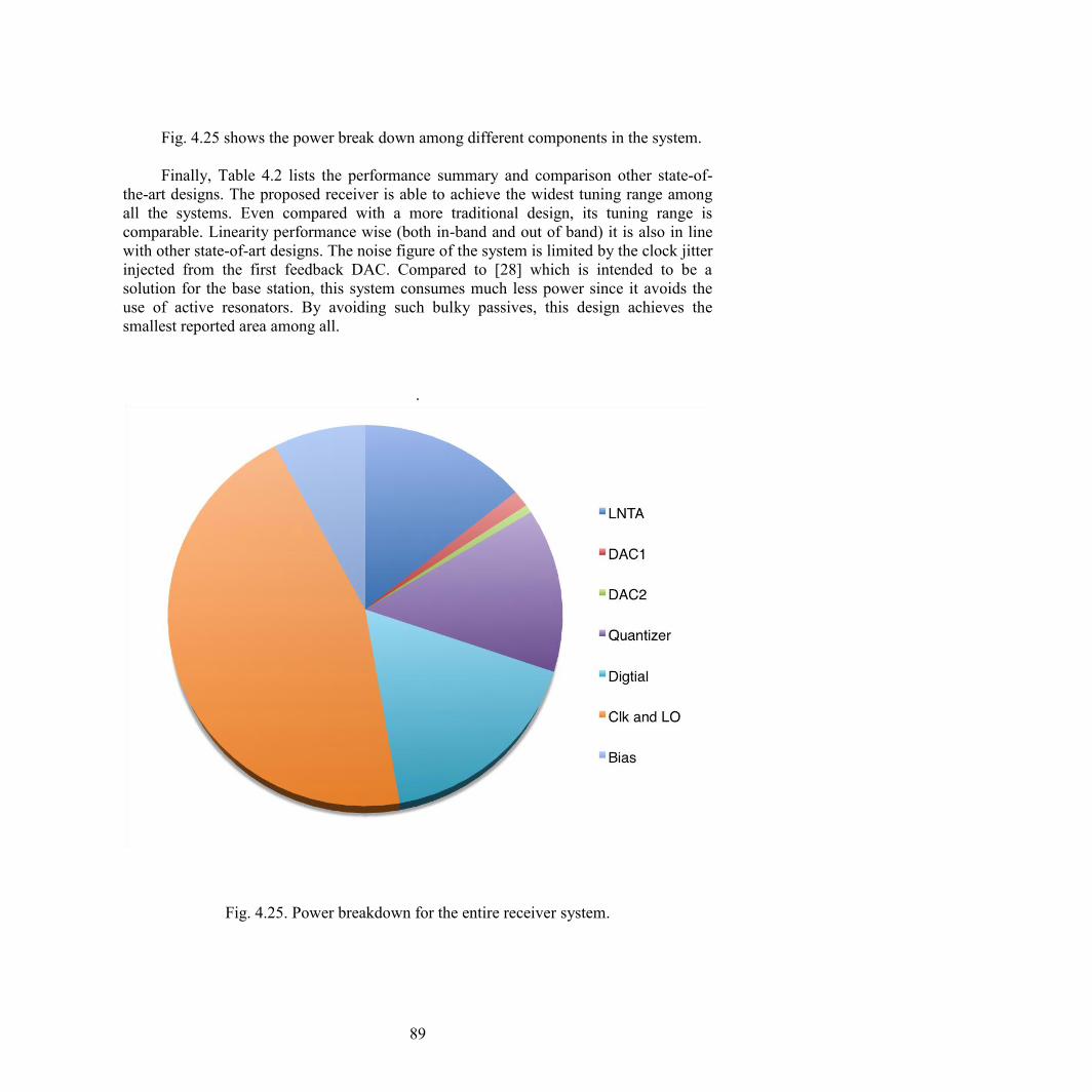
89
Fig. 4.25 shows the power break down among different components in the system.
Finally, Table 4.2 lists the performance summary and comparison other state-of-
the-art designs. The proposed receiver is able to achieve the widest tuning range among
all the systems. Even compared with a more traditional design, its tuning range is
comparable. Linearity performance wise (both in-band and out of band) it is also in line
with other state-of-art designs. The noise figure of the system is limited by the clock jitter
injected from the first feedback DAC. Compared to [28] which is intended to be a
solution for the base station, this system consumes much less power since it avoids the
use of active resonators. By avoiding such bulky passives, this design achieves the
smallest reported area among all.
.
Fig. 4.25. Power breakdown for the entire receiver system.
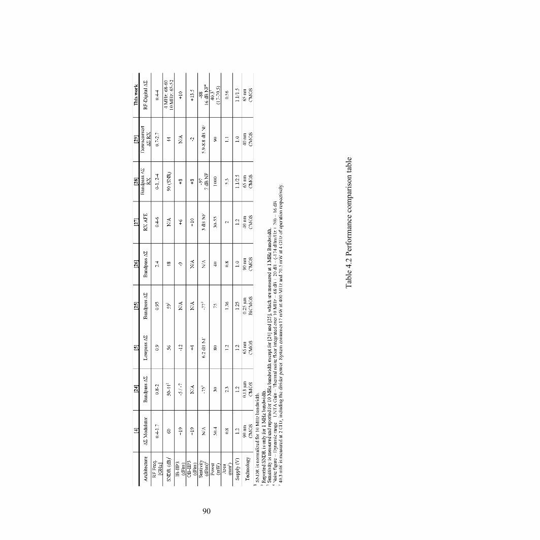
90
Tab
le 4
.2 P
erfo
rman
ce c
om
par
ison t
able
91
4.4. CONCLUSION
This chapter presents an experimental prototype ADC based receiver design that
supports a frequency of operation from 400 MHz to 4000 MHz, which covers the entire
LTE bands worldwide. An NRZ feedback DAC design reduces the jitter sensitivity of the
system, and aids in achieving a high SNDR over the frequency range of interest. It
provides a large dynamic range with a low power consumption. It meets the three major
criteria of the SDR systems. Without any bulky passives, the design maintains its small
footprint, while digital-oriented design methodology enables a truly flexible receiver that
is able to adapt to different standards with change of a couple control bits. Finally, the
solution can scale naturally with technology.
92
Chapter 5
Mixer-First Receiver Design Considerations
5.1 Introduction to the Passive CMOS Mixer
Contradicting the conventional belief that analog/RF circuitry does not scale well
with shrinking technology, the CMOS passive mixer is one of the few RF components
that have most benefited from the process scaling. Passive mixers based on CMOS
technology has been proposed earlier [57][58]. However, they did not attract much
attention until the CMOS technology marched into the deep sub-micron region in the late
2000’s. The recent improvements to CMOS technology empower the passive mixer
designs, as they supersede active mixers designs in industrial designs and academia
endeavors [59][60]. Compared to its active mixing peer, a passive mixer has one
additional feature which is known as bi-directionality. Ironically, this unique property
used to be considered major downside for the passive mixer, since it lacks the reverse
isolation (S21=S12) as most of the conventional RF circuits can provide. Furthermore, bi-
directionality makes the analysis for a passive mixer so obscure that for a fairly long
time, engineering intuition was hard to obtain. Fortunately, recent research efforts such as
[59] have cleared up the obstacles. It has been shown by multiple sources that this two-
way frequency translation feature of passive mixers provides a series of benefits over
active mixers, therefore, new opportunities together with unique design challenges arise.
There are two primary differences between a passive mixer and an active mixer
design. One is the feature of bi-directionality. Due to the absence of reverse isolation,
passive mixers can down-convert the RF signal to the baseband and at the same time up-
convert the baseband signal to the RF band. When the passive mixer switches turn on, the
switches are transparent, only presenting their on-impedance, and they don’t favor one
port over the other. This is in contrast to case of an active mixer, where the Gilbert cells
behave as the common-gate amplifiers. The passive feature of the passive mixer has long
been considered a disadvantage, since the mixer cannot provide any power gain, thus
limiting the overall system’s noise performance. Moreover, the absence of reverse
isolation in a passive mixer often brought up concerns about the robustness of the design.
Interestingly, scientific research sometimes takes an unexpected turn, and this “annoying”
transparency feature has turned out to be the very reason that the passive mixer is so
popular now. The transparent feature allows the signal to translate to different
frequencies, as well as allows for impedance frequency translation.
93
Another major difference between a passive mixer and an active mixer is the
absence of DC bias current. The absence of the DC bias current takes away the origin of
the low-frequency flicker noise. Therefore, with proper design, RF system with
embedded passive mixers can achieve much better tradeoff between power and
performance compared to designs adopting active mixers.
Recent research has shown that by utilizing multiple non-overlapping LO
waveforms, the passive mixer designs can be better optimized compared with the use of a
more traditional sinusoidal or simple square-wave LO waveforms [58][60][63][64][65].
Each of the clock pulses drives a different mixer switch. Together, a series of phase-
shifted baseband outputs can be generated, and they can later be summed with the
baseband trans-impedance amplifier (TIA) to reconstruct the complete baseband output.
5.2 Passive Mixer-First Receiver Design Basics
Back in Chapter 2, the concept of digitally-assisted RF receiver design has been
introduced. These designs aim to minimize the component count of the RF front-end
design. The passive mixer-first receiver architectures stands at the forefront of the
movement towards minimalism in design methodology, which draws upon innovations
based on recent studies on the passive mixer. A mixer-first system can be simply
described as a receiver topology without the RF amplification stage (LNA or LNTA).
Recent research effort has demystified the passive mixer, and the idea of the passive
mixer-first design has gained a lot of momentum in different kinds of wireless
applications.
To understand the idea of passive-mixer first receiver designs, it is better to start
with explaining how a multi-phase passive mixer network operates. Fig. 5.1 shows a
simple circuit model for a 4-phase passive mixer network, and Fig. 5.2 shows the four
clock waveforms driving each of the four phases in a passive mixer system. One
fundamental
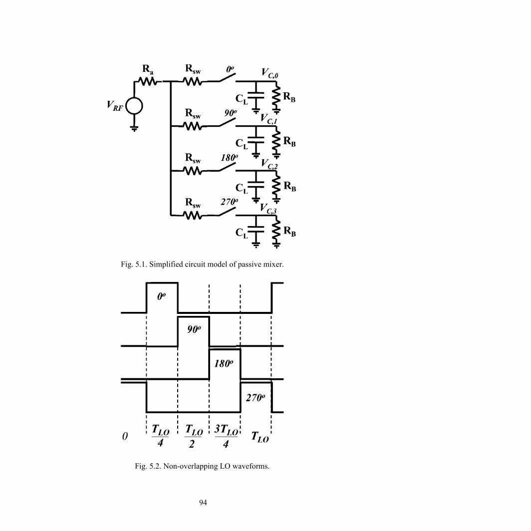
94
Fig. 5.1. Simplified circuit model of passive mixer.
Fig. 5.2. Non-overlapping LO waveforms.
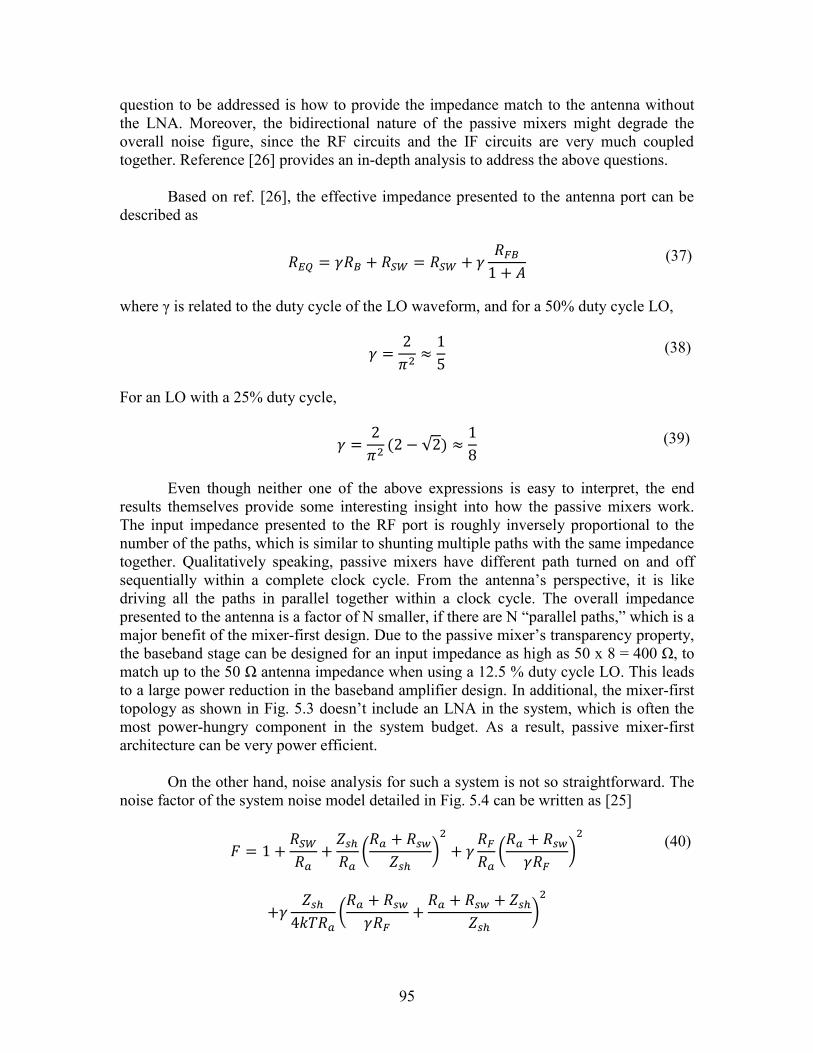
95
question to be addressed is how to provide the impedance match to the antenna without
the LNA. Moreover, the bidirectional nature of the passive mixers might degrade the
overall noise figure, since the RF circuits and the IF circuits are very much coupled
together. Reference [26] provides an in-depth analysis to address the above questions.
Based on ref. [26], the effective impedance presented to the antenna port can be
described as
where γ is related to the duty cycle of the LO waveform, and for a 50% duty cycle LO,
For an LO with a 25% duty cycle,
√
Even though neither one of the above expressions is easy to interpret, the end
results themselves provide some interesting insight into how the passive mixers work.
The input impedance presented to the RF port is roughly inversely proportional to the
number of the paths, which is similar to shunting multiple paths with the same impedance
together. Qualitatively speaking, passive mixers have different path turned on and off
sequentially within a complete clock cycle. From the antenna’s perspective, it is like
driving all the paths in parallel together within a clock cycle. The overall impedance
presented to the antenna is a factor of N smaller, if there are N “parallel paths,” which is a
major benefit of the mixer-first design. Due to the passive mixer’s transparency property,
the baseband stage can be designed for an input impedance as high as 50 x 8 = 400 Ω, to
match up to the 50 Ω antenna impedance when using a 12.5 % duty cycle LO. This leads
to a large power reduction in the baseband amplifier design. In additional, the mixer-first
topology as shown in Fig. 5.3 doesn’t include an LNA in the system, which is often the
most power-hungry component in the system budget. As a result, passive mixer-first
architecture can be very power efficient.
On the other hand, noise analysis for such a system is not so straightforward. The
noise factor of the system noise model detailed in Fig. 5.4 can be written as [25]
(
)
(
)
(
)
(37)
(38)
(39)
(40)
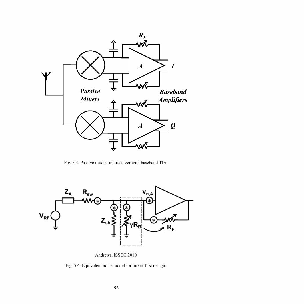
96
Fig. 5.3. Passive mixer-first receiver with baseband TIA.
Andrews, ISSCC 2010
Fig. 5.4. Equivalent noise model for mixer-first design.
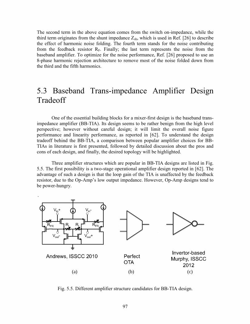
97
The second term in the above equation comes from the switch on-impedance, while the
third term originates from the shunt impedance Zsh, which is used in Ref. [26] to describe
the effect of harmonic noise folding. The fourth term stands for the noise contributing
from the feedback resistor RF. Finally; the last term represents the noise from the
baseband amplifier. To optimize for the noise performance, Ref. [26] proposed to use an
8-phase harmonic rejection architecture to remove most of the noise folded down from
the third and the fifth harmonics.
5.3 Baseband Trans-impedance Amplifier Design
Tradeoff
One of the essential building blocks for a mixer-first design is the baseband trans-
impedance amplifier (BB-TIA). Its design seems to be rather benign from the high level
perspective; however without careful design; it will limit the overall noise figure
performance and linearity performance, as reported in [62]. To understand the design
tradeoff behind the BB-TIA, a comparison between popular amplifier choices for BB-
TIAs in literature is first presented, followed by detailed discussion about the pros and
cons of each design, and finally, the desired topology will be highlighted.
Three amplifier structures which are popular in BB-TIA designs are listed in Fig.
5.5. The first possibility is a two-stage operational amplifier design reported in [62]. The
advantage of such a design is that the loop gain of the TIA is unaffected by the feedback
resistor, due to the Op-Amp’s low output impedance. However, Op-Amp designs tend to
be power-hungry.
.
(a) (b) (c)
Fig. 5.5. Different amplifier structure candidates for BB-TIA design.
98
An operational transconductance amplifier (OTA) as shown in Fig. 5.5, on the
other hand, would be loaded by the feedback resistors, assuming its output impedance is
much larger than the feedback resistors. In this case, the loop gain is set by the feedback
resistors. However, for CMOS technology in the deep sub-micron region, the devices’
output impedance is quite limited, and hence the loop gain of the BB-TIA is set by the
shunt impedance between feedback resistors and the output impedance of the OTA. As
shown later in this section, this does have a negative effect on the overall noise
performance due to the gm noise component.
An inverter-based TIA design was recently reported in [68]. An inverter-based
amplifier design has some really interesting properties due to its mid-range output
impedance. With a large feedback resistor, the design behaves like an op-amp, while the
inverter-based amplifier behaves like an OTA with a smaller feedback resistor.
Moreover, the inverter-based amplifier can provide a large dynamic current in the
presence of a blocker to maintain its linearity performance over a large signal transient.
Based on the derivations for a general shunt-shunt feedback network from [73], it
can be shown that the input impedance of an Op-Amp based TIA like [62] can be
expressed as
By a similar analysis, it can be shown that the OTA-based TIA’s input impedance
can be expressed as
For an inverter-based TIA design, the input impedance can be described as
||
(41)
(42)
(43)
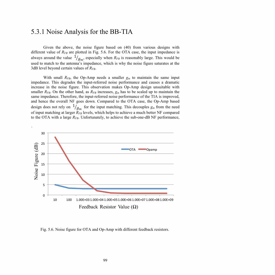
99
5.3.1 Noise Analysis for the BB-TIA
Given the above, the noise figure based on (40) from various designs with
different value of RFB are plotted in Fig. 5.6. For the OTA case, the input impedance is
always around the value
⁄ , especially when RFB is reasonably large. This would be
used to match to the antenna’s impedance, which is why the noise figure saturates at the
3dB level beyond certain values of RFB.
With small RFB, the Op-Amp needs a smaller gm to maintain the same input
impedance. This degrades the input-referred noise performance and causes a dramatic
increase in the noise figure. This observation makes Op-Amp design unsuitable with
smaller RFB. On the other hand, as RFB increases, gm has to be scaled up to maintain the
same impedance. Therefore, the input-referred noise performance of the TIA is improved,
and hence the overall NF goes down. Compared to the OTA case, the Op-Amp based
design does not rely on
⁄ for the input matching. This decouples gm from the need
of input matching at larger RFB levels, which helps to achieve a much better NF compared
to the OTA with a large RFB. Unfortunately, to achieve the sub-one-dB NF performance,
.
Fig. 5.6. Noise figure for OTA and Op-Amp with different feedback resistors.
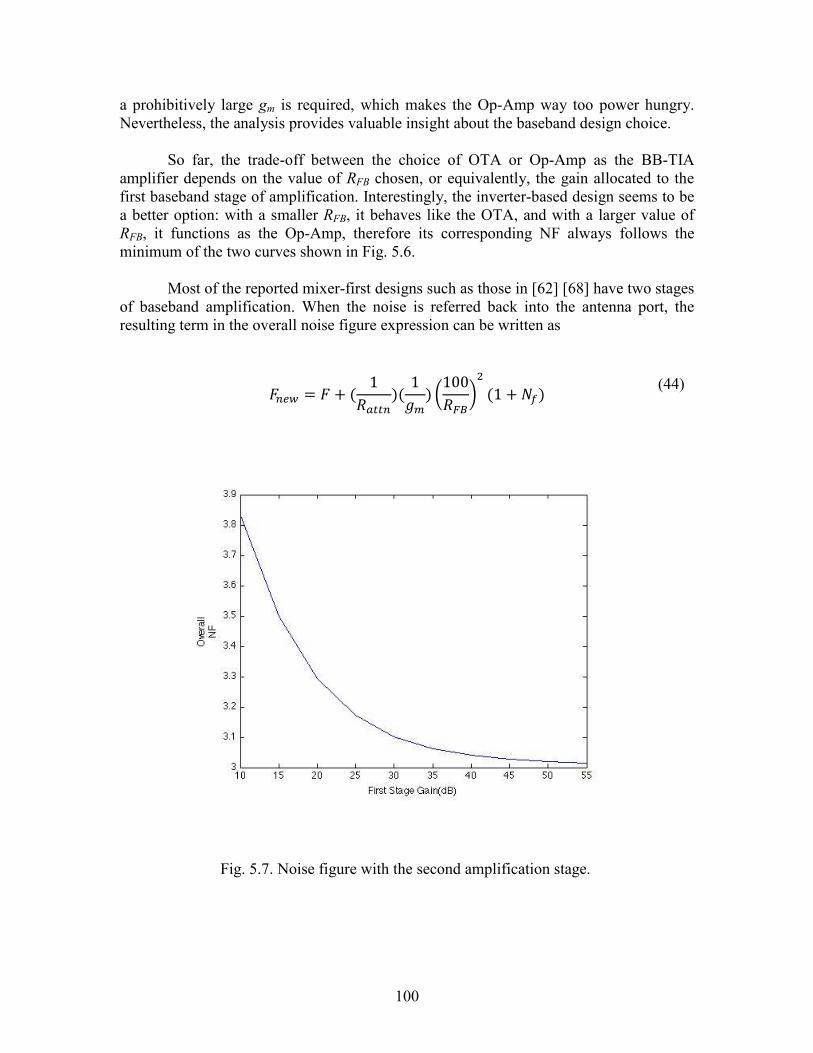
100
a prohibitively large gm is required, which makes the Op-Amp way too power hungry.
Nevertheless, the analysis provides valuable insight about the baseband design choice.
So far, the trade-off between the choice of OTA or Op-Amp as the BB-TIA
amplifier depends on the value of RFB chosen, or equivalently, the gain allocated to the
first baseband stage of amplification. Interestingly, the inverter-based design seems to be
a better option: with a smaller RFB, it behaves like the OTA, and with a larger value of
RFB, it functions as the Op-Amp, therefore its corresponding NF always follows the
minimum of the two curves shown in Fig. 5.6.
Most of the reported mixer-first designs such as those in [62] [68] have two stages
of baseband amplification. When the noise is referred back into the antenna port, the
resulting term in the overall noise figure expression can be written as
(
)
Fig. 5.7. Noise figure with the second amplification stage.
(44)
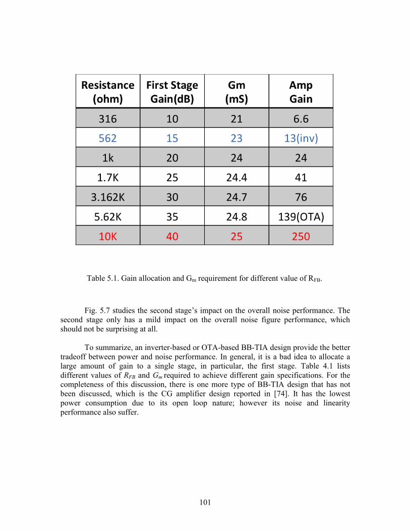
101
Fig. 5.7 studies the second stage’s impact on the overall noise performance. The
second stage only has a mild impact on the overall noise figure performance, which
should not be surprising at all.
To summarize, an inverter-based or OTA-based BB-TIA design provide the better
tradeoff between power and noise performance. In general, it is a bad idea to allocate a
large amount of gain to a single stage, in particular, the first stage. Table 4.1 lists
different values of RFB and Gm required to achieve different gain specifications. For the
completeness of this discussion, there is one more type of BB-TIA design that has not
been discussed, which is the CG amplifier design reported in [74]. It has the lowest
power consumption due to its open loop nature; however its noise and linearity
performance also suffer.
Table 5.1. Gain allocation and Gm requirement for different value of RFB.
102
5.3.1 Analysis for BB-TIA Out-of-Band Linearity
Out-of-band (OOB) linearity performance is one of the key performance metrics
in describing the receiver’s blocker resilience. As a receiver has no control over its input
statistics, when the receiver is jammed by a large interference in a nearby frequency, the
receiver is expected to still maintain its functionality with minimum performance
degradation. This really stresses the importance of the out-of-band linearity performance
of a receiver.
Most of the time, baseband amplifiers set the linearity limits. Due to the mixer-
first design’s simple topology, the BB-TIA is the first stage to provide amplification;
therefore it is also the first stage to experience linearity degradation. The passive CMOS
mixer switches, to the first order, are functioning as switches. The signal voltages on the
two ends of the switches are retained to their minimum since the switches do not provide
any power gain. Therefore, the switches tend to have a good linearity performance.
To improve the out-of-band linearity performance, reducing the OOB blocker as
early as possible is essential. Recent passive mixer-first designs [62] [68] rely heavily on
CL in Fig. 5.1 for attenuating the blocker right after down-conversion so that the large
blocker does not make its way into the BB-TIA or the rest of the system. Hence, a good
OOB linearity performance can be preserved.
However, the possible frequency locations of the blockers vary drastically from
one standard to another. For some standards, such as GSM, a reasonably large
interference presented at 40 MHz away from the carrier frequency might easily saturate
the receiver system. To accommodate a relatively close-in jammer, the CL required for
the passive-mixer-first design might be prohibitively large. Ref [62] has reported of using
a CL as large as 100 pF, which results in a large area overhead and, hence, a large silicon
production cost.
To quantify the issue, a design example of the mixer-first design is provided.
Assume the baseband amplifier has an in-band IIP3 of -20 dBm, and the CMOS mixer
switches have an on-impedance of 20 Ω. Table 5.2 shows the relationship between OOB
filtering and OOB IIP3
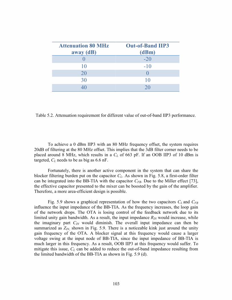
103
To achieve a 0 dBm IIP3 with an 80 MHz frequency offset, the system requires
20dB of filtering at the 80 MHz offset. This implies that the 3dB filter corner needs to be
placed around 8 MHz, which results in a CL of 663 pF. If an OOB IIP3 of 10 dBm is
targeted, CL needs to be as big as 6.6 nF.
Fortunately, there is another active component in the system that can share the
blocker filtering burden put on the capacitor CL. As shown in Fig. 5.8, a first-order filter
can be integrated into the BB-TIA with the capacitor CFB. Due to the Miller effect [73],
the effective capacitor presented to the mixer can be boosted by the gain of the amplifier.
Therefore, a more area-efficient design is possible.
Fig. 5.9 shows a graphical representation of how the two capacitors CL and CFB
influence the input impedance of the BB-TIA. As the frequency increases, the loop gain
of the network drops. The OTA is losing control of the feedback network due to its
limited unity gain bandwidth. As a result, the input impedance RIN would increase, while
the imaginary part CIN would diminish. The overall input impedance can then be
summarized as ZIN, shown in Fig. 5.9. There is a noticeable kink just around the unity
gain frequency of the OTA. A blocker signal at this frequency would cause a larger
voltage swing at the input node of BB-TIA, since the input impedance of BB-TIA is
much larger in this frequency. As a result, OOB IIP3 at this frequency would suffer. To
mitigate this issue, CL can be added to reduce the out-of-band impedance resulting from
the limited bandwidth of the BB-TIA as shown in Fig. 5.9 (d).
Attenuation 80 MHz
away (dB)
Out-of-Band IIP3
(dBm)
0 -20
10 -10
20 0
30 10
40 20
Table 5.2. Attenuation requirement for different value of out-of-band IIP3 performance.
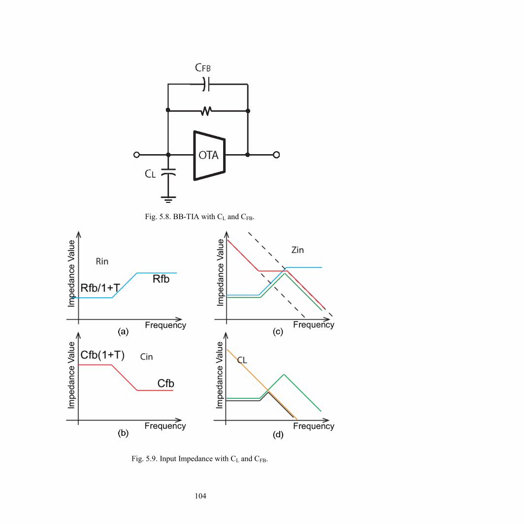
104
Fig. 5.8. BB-TIA with CL and CFB.
Fig. 5.9. Input Impedance with CL and CFB.
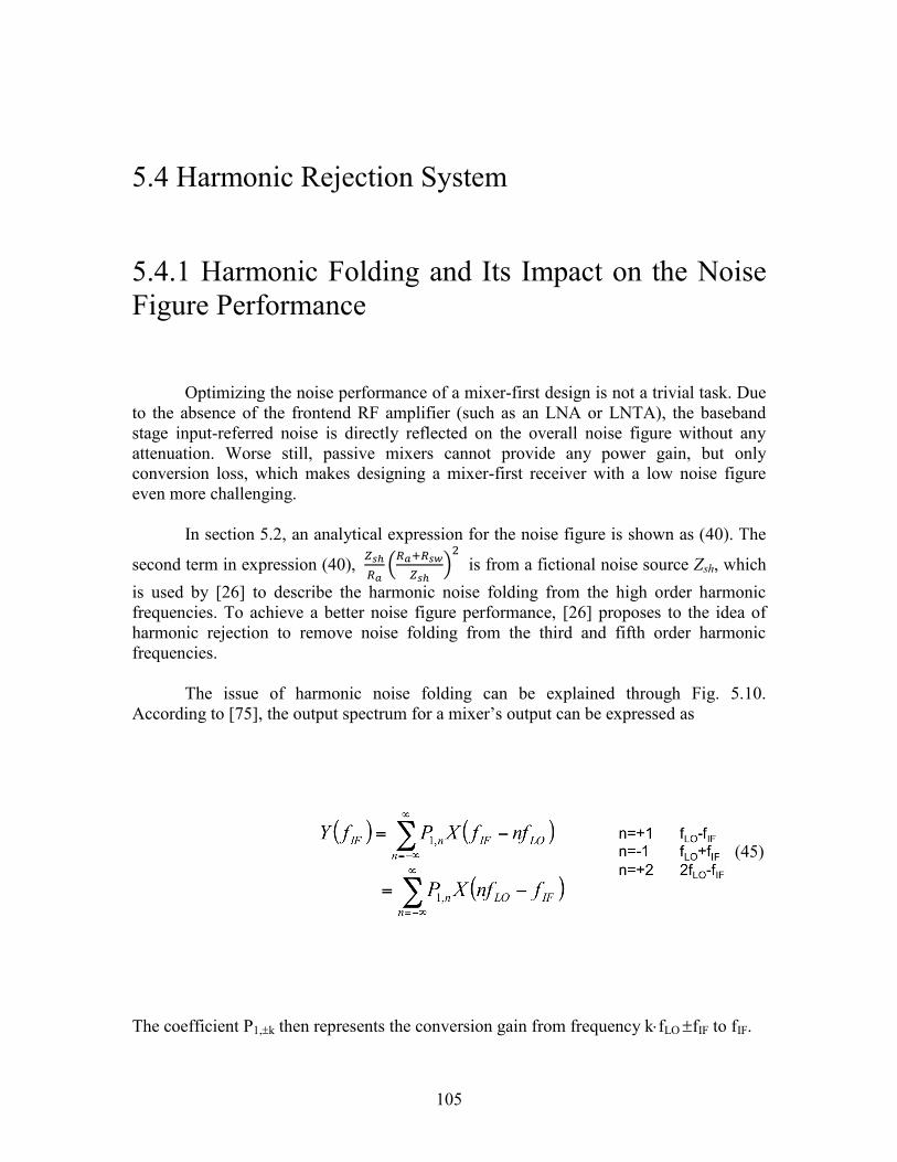
105
5.4 Harmonic Rejection System
5.4.1 Harmonic Folding and Its Impact on the Noise
Figure Performance
Optimizing the noise performance of a mixer-first design is not a trivial task. Due
to the absence of the frontend RF amplifier (such as an LNA or LNTA), the baseband
stage input-referred noise is directly reflected on the overall noise figure without any
attenuation. Worse still, passive mixers cannot provide any power gain, but only
conversion loss, which makes designing a mixer-first receiver with a low noise figure
even more challenging.
In section 5.2, an analytical expression for the noise figure is shown as (40). The
second term in expression (40),
(
)
is from a fictional noise source Zsh, which
is used by [26] to describe the harmonic noise folding from the high order harmonic
frequencies. To achieve a better noise figure performance, [26] proposes to the idea of
harmonic rejection to remove noise folding from the third and fifth order harmonic
frequencies.
The issue of harmonic noise folding can be explained through Fig. 5.10.
According to [75], the output spectrum for a mixer’s output can be expressed as
The coefficient P1,k then represents the conversion gain from frequency kfLO fIF to fIF.
(45)
106
Through some manipulation of the above equations [75], it can be shown that if
(white), then
∫
∑| |
Where, for a square wave p1(t), .
The noise for the first pair of sidebands (fLOfIF) accounts for
of the overall noise. The noise from the third pair (3fLOfIF) accounts for
of the total noise. The remaining harmonics account for the rest of the noise, which
is around 10%. This suggests that removing the noise folding from the third and fifth
harmonics can improve the system noise figure performance.
Fig. 5.10.Harmonic noise folding.
(46)
(47)
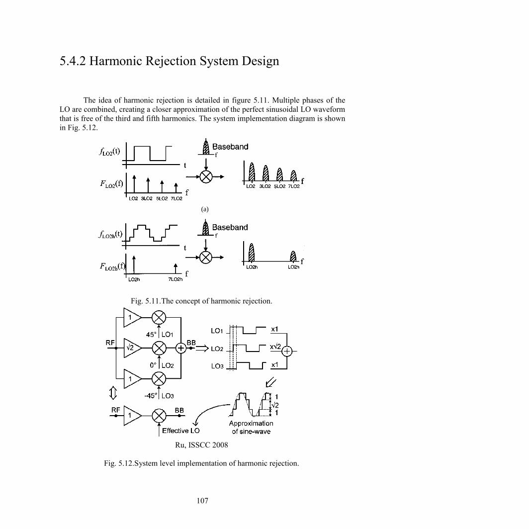
107
5.4.2 Harmonic Rejection System Design
The idea of harmonic rejection is detailed in figure 5.11. Multiple phases of the
LO are combined, creating a closer approximation of the perfect sinusoidal LO waveform
that is free of the third and fifth harmonics. The system implementation diagram is shown
in Fig. 5.12.
Fig. 5.11.The concept of harmonic rejection.
Ru, ISSCC 2008
Fig. 5.12.System level implementation of harmonic rejection.
2006 IEEE JOURNAL OF SOLID-STATE CIRCUITS, VOL. 36, NO. 12, DECEMBER 2001
(a)
(b)
Fig. 5. (a) Conventional switching mixer. (b) Harmonic-rejectionfundamentals.
Fig. 6. Harmonic-rejection signal generation.
at seven times the fundamental frequency, the first significant
copy of the upconverted baseband signal is also located at
seven times the fundamental frequency. Consequently, the IF
filtering requirement is greatly relaxed, leading to removal of
the IF filter. The next challenge was to generate while
maintaining the advantages of using a current-commutating
switching mixer. Current-commutating switching mixers allow
for a relatively low LO swing, which is critical for integration
using low- components.
To generate , three square waves are summed as
shown in Fig. 6. To accurately represent a quantized sinusoid,
the magnitude of is scaled by . To better understand
the rejection of the third and fifth harmonics, it is instructive
to expand the three square waves using a Fourier series. The
Fourier series representation of the three square waves up to the
fifth-order component is given by
(1)
(2)
(a)
(b)
Fig. 7. Harmonic-rejection with mismatch. (a) For third harmonic. (b) For fifthharmonic.
(3)
Summing the three ideal square waves with scaled by
results in the total rejection of the third and fifth harmonics.
However, similar to a single-sideband mixer, gain and phase
mismatch result in nonideal cancellation of the third and fifth
harmonics. The rejection of the third and fifth harmonic are
given by
(4)
(5)
where is the gain mismatch and is the phase mismatch.
The rejection depends strongly on the phase error in the original
signal. Shown in Fig. 7 is the harmonic rejection plotted as a
function of phase error for different gain errors. Fig. 7(a) shows
the rejection of the third harmonic while Fig. 7(b) shows the
rejection of the fifth harmonic. Note that as the phase and gain
error increase the rejection of the third harmonic approaches
9.5 dBc while the rejection of the fifth harmonic approaches
14 dBc, which are the levels of an ideal square wave. For one-
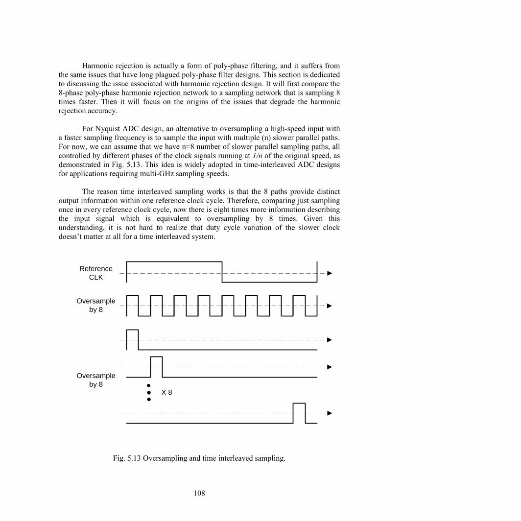
108
Harmonic rejection is actually a form of poly-phase filtering, and it suffers from
the same issues that have long plagued poly-phase filter designs. This section is dedicated
to discussing the issue associated with harmonic rejection design. It will first compare the
8-phase poly-phase harmonic rejection network to a sampling network that is sampling 8
times faster. Then it will focus on the origins of the issues that degrade the harmonic
rejection accuracy.
For Nyquist ADC design, an alternative to oversampling a high-speed input with
a faster sampling frequency is to sample the input with multiple (n) slower parallel paths.
For now, we can assume that we have n=8 number of slower parallel sampling paths, all
controlled by different phases of the clock signals running at 1/n of the original speed, as
demonstrated in Fig. 5.13. This idea is widely adopted in time-interleaved ADC designs
for applications requiring multi-GHz sampling speeds.
The reason time interleaved sampling works is that the 8 paths provide distinct
output information within one reference clock cycle. Therefore, comparing just sampling
once in every reference clock cycle, now there is eight times more information describing
the input signal which is equivalent to oversampling by 8 times. Given this
understanding, it is not hard to realize that duty cycle variation of the slower clock
doesn’t matter at all for a time interleaved system.
Fig. 5.13 Oversampling and time interleaved sampling.
X 8
Reference
CLK
Oversample
by 8
Oversample
by 8
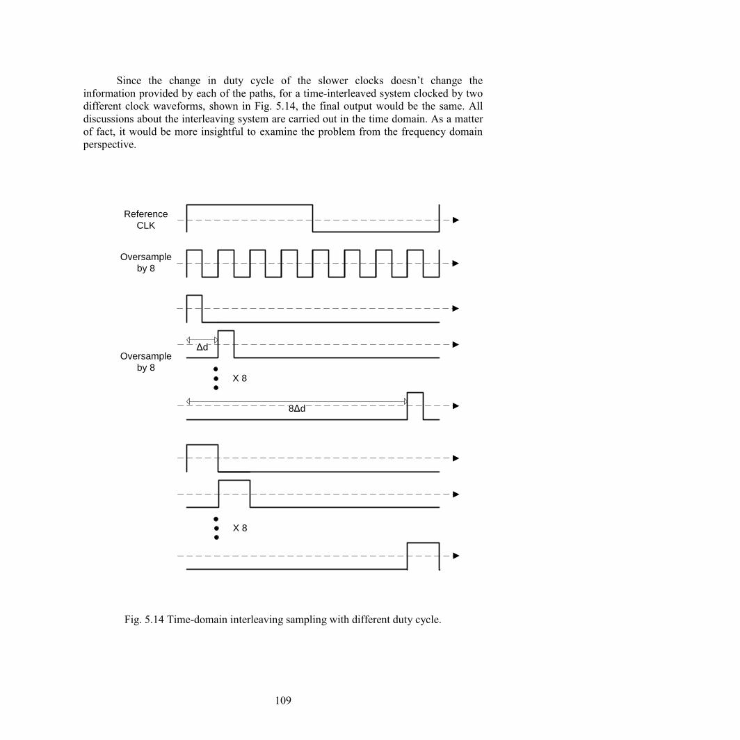
109
Since the change in duty cycle of the slower clocks doesn’t change the
information provided by each of the paths, for a time-interleaved system clocked by two
different clock waveforms, shown in Fig. 5.14, the final output would be the same. All
discussions about the interleaving system are carried out in the time domain. As a matter
of fact, it would be more insightful to examine the problem from the frequency domain
perspective.
Fig. 5.14 Time-domain interleaving sampling with different duty cycle.
X 8
Reference
CLK
Oversample
by 8
Oversample
by 8
X 8
Δd
8Δd
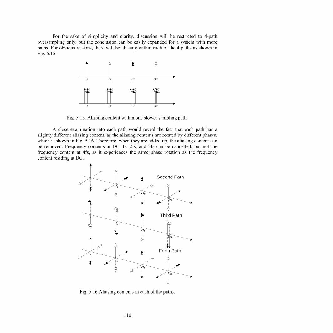
110
For the sake of simplicity and clarity, discussion will be restricted to 4-path
oversampling only, but the conclusion can be easily expanded for a system with more
paths. For obvious reasons, there will be aliasing within each of the 4 paths as shown in
Fig. 5.15.
Fig. 5.15. Aliasing content within one slower sampling path.
A close examination into each path would reveal the fact that each path has a
slightly different aliasing content, as the aliasing contents are rotated by different phases,
which is shown in Fig. 5.16. Therefore, when they are added up, the aliasing content can
be removed. Frequency contents at DC, fs, 2fs, and 3fs can be cancelled, but not the
frequency content at 4fs, as it experiences the same phase rotation as the frequency
content residing at DC.
Fig. 5.16 Aliasing contents in each of the paths.
0 fs 2fs 3fs
0 fs 2fs 3fs
0
fs
2fs
3fs
Third Path
0
fs
2fs
3fs
Second Path
0
fs
2fs
3fs
Forth Path
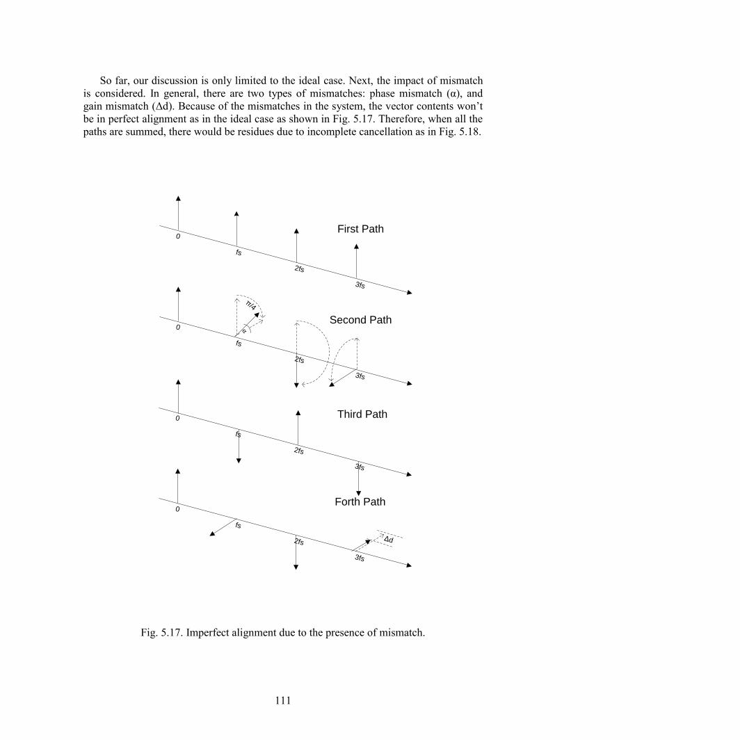
111
So far, our discussion is only limited to the ideal case. Next, the impact of mismatch
is considered. In general, there are two types of mismatches: phase mismatch (α), and
gain mismatch (Δd). Because of the mismatches in the system, the vector contents won’t
be in perfect alignment as in the ideal case as shown in Fig. 5.17. Therefore, when all the
paths are summed, there would be residues due to incomplete cancellation as in Fig. 5.18.
Fig. 5.17. Imperfect alignment due to the presence of mismatch.
0
fs
2fs
3fs
Third Path
0
fs
2fs
3fs
Second Path
0
fs
2fs
3fs
Forth Path
0
fs
2fs
3fs
First Path
π/4
α
Δd

112
Fig. 5.18 Incomplete harmonic cancelation due to phase and gain mismatch.
Mismatch limits the overall performance (in the case of an ADC, they result in
distortion tones) as demonstrated in Fig. 5.19. In general, the resolution is limited to 6-8
bits due to the limited matching between components such as capacitors and resistors (
1% element mismatch translates to ~ 40 dB harmonic rejection performance). More paths
might help, since the mismatches among all paths tend to average out, but this comes
with a huge power and area penalty. Fig. 5.20 provides a behavioral model for studying
atime-interleave system under phase and gain mismatches.
Fig. 5.19 Performance limitation due to mismatches.
0
fs
2fs
3fs
Sum of 4 Paths
Δd
0 fs 2fs 3fs 4fs 5fs 6fs
0 fs 2fs 3fs 4fs 5fs 6fs
0 fs 2fs 3fs 4fs 5fs 6fs
Typical DT
Sampling
Oversampled
by 4
Residue due
to mismatch
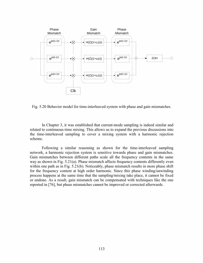
113
Fig. 5.20 Behavior model for time-interleaved system with phase and gain mismatches.
In Chapter 3, it was established that current-mode sampling is indeed similar and
related to continuous-time mixing. This allows us to expand the previous discussions into
the time-interleaved sampling to cover a mixing system with a harmonic rejection
scheme.
Following a similar reasoning as shown for the time-interleaved sampling
network, a harmonic rejection system is sensitive towards phase and gain mismatches.
Gain mismatches between different paths scale all the frequency contents in the same
way as shown in Fig. 5.21(a). Phase mismatch affects frequency contents differently even
within one path as in Fig. 5.21(b). Noticeably, phase mismatch results in more phase shift
for the frequency content at high order harmonic. Since this phase winding/unwinding
process happens at the same time that the sampling/mixing take place, it cannot be fixed
or undone. As a result, gain mismatch can be compensated with techniques like the one
reported in [76], but phase mismatches cannot be improved or corrected afterwards.
ejw(1-1)τ
H(Z)(1+ε1(z)) ejw(1-1)τ
ejw(i-1)τ
H(Z)(1+εi(z)) ejw(i-1)τ
ejw(n-1)τ
H(Z)(1+εn(z)) ejw(n-1)τ
ZOH
Clk
Phase
Mismatch
Gain
Mismatch
Phase
Mismatch
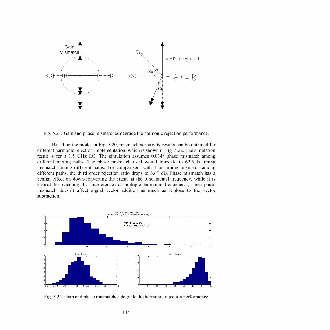
114
Fig. 5.21. Gain and phase mismatches degrade the harmonic rejection performance.
Based on the model in Fig. 5.20, mismatch sensitivity results can be obtained for
different harmonic rejection implementation, which is shown in Fig. 5.22. The simulation
result is for a 1.5 GHz LO. The simulation assumes 0.034° phase mismatch among
different mixing paths. The phase mismatch used would translate to 62.5 fs timing
mismatch among different paths. For comparison, with 1 ps timing mismatch among
different paths, the third order rejection ratio drops to 33.7 dB. Phase mismatch has a
benign effect on down-converting the signal at the fundamental frequency, while it is
critical for rejecting the interferences at multiple harmonic frequencies, since phase
mismatch doesn’t affect signal vector addition as much as it does to the vector
subtraction.
Fig. 5.22. Gain and phase mismatches degrade the harmonic rejection performance
Gain
Mismatch
3αα
2α
α – Phase Mismatch
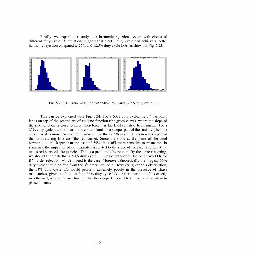
115
Finally, we expand our study to a harmonic rejection system with clocks of
different duty cycles. Simulations suggest that a 50% duty cycle can achieve a better
harmonic rejection compared to 25% and 12.5% duty cycle LOs, as shown in Fig. 5.23.
Fig. 5.23. HR ratio measured with 50%, 25% and 12.5% duty cycle LO
This can be explained with Fig. 5.24. For a 50% duty cycle, the 3rd
harmonic
lands on top of the second arc of the sinc function (the green curve), where the slope of
the sinc function is close to zero. Therefore, it is the least sensitive to mismatch. For a
25% duty cycle, the third harmonic content lands in a steeper part of the first arc (the blue
curve), so it is more sensitive to mismatch. For the 12.5% case, it lands in a steep part of
the far-stretching first arc (the red curve). Since the slope at the point of the third
harmonic is still larger than the case of 50%, it is still more sensitive to mismatch. In
summary, the impact of phase mismatch is related to the slope of the sinc function at the
undesired harmonic frequencies. This is a profound observation. By the same reasoning,
we should anticipate that a 50% duty cycle LO would outperform the other two LOs for
fifth order rejection, which indeed is the case. Moreover, theoretically the magical 33%
duty cycle should be free from the 3rd
order harmonic. However, given this observation,
the 33% duty cycle LO would perform extremely poorly in the presence of phase
mismatches, given the fact that for a 33% duty cycle LO the third harmonic falls exactly
into the null, where the sinc function has the steepest slope. Thus, it is more sensitive to
phase mismatch.
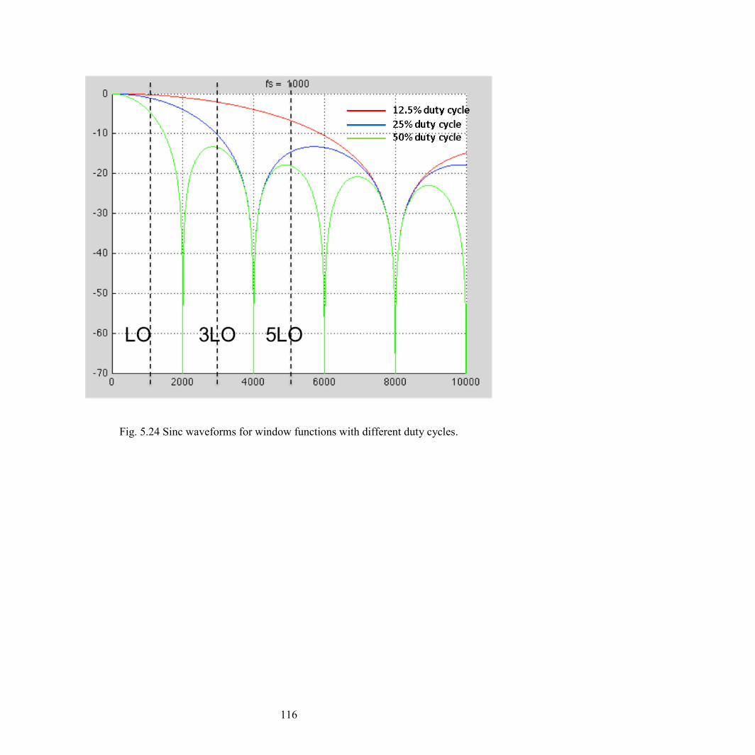
116
Fig. 5.24 Sinc waveforms for window functions with different duty cycles.
117
CHAPTER 5 APPENDIX:
Mixer Linearity Analysis
Reference [114] shows a general Volterra analysis for double balanced passive
mixer with 50% duty clock. This section intends to extend it to cover the HR case. The
signal current content can be expressed as
where the vd and vs are the drain and source voltages respectively of the transistor device.
The input and output voltages can be expressed as a converging Volterra series of the
source current iRF. It follows,
where Hns and Hnd are the according nth-order Volterra kernels for the drain and the
source nodes of the passive mixer, respectively. The voltage swing at the source node can
be written as
118
The first-order Volterra kernels for the source node can be written as
For the drain node, it can be shown as
The in the above equation is the frequency conversion loss due to the mixing
operation, which is related to duty cycle of LO. For a 50% duty cycle clock it can be
shown as
. While for 25% and 12.5% duty cycle it can be shown as
and
√ . Then, the first-order Volterra kernels at the drain node can be expressed as
The second order kernels for the drain and source nodes can be
( )( )

119
In a similar fashion, the second order Volterra kenerls can then be shown as
The third order of Volterra kernerls can be shown as
Now the discussion can be further extended to derive the expressions for IIP2 and IIP3
for a mixer first design. It can be shown that
120
( )
Also, reference [114] introduces a new metric XM IIP3 for three tone case, by a similar
steps, it can be expressed as
Now, let’s introduce the effect of the source and load impedance which would have a
serious impact on mixer’ linearity performance.
∑
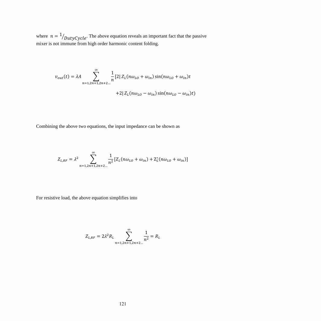
121
where ⁄ . The above equation reveals an important fact that the passive
mixer is not immune from high order harmonic content folding.
∑
|
|
Combining the above two equations, the input impedance can be shown as
∑
For resistive load, the above equation simplifies into
∑
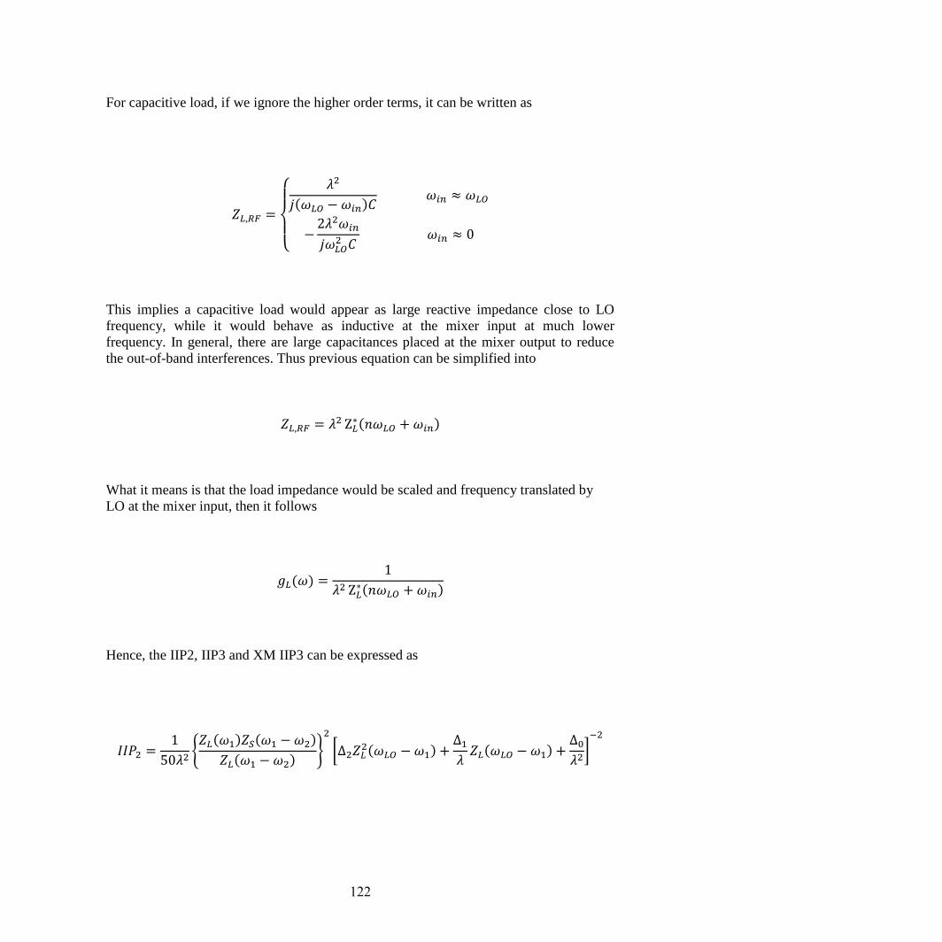
122
For capacitive load, if we ignore the higher order terms, it can be written as
This implies a capacitive load would appear as large reactive impedance close to LO
frequency, while it would behave as inductive at the mixer input at much lower
frequency. In general, there are large capacitances placed at the mixer output to reduce
the out-of-band interferences. Thus previous equation can be simplified into
What it means is that the load impedance would be scaled and frequency translated by
LO at the mixer input, then it follows
Hence, the IIP2, IIP3 and XM IIP3 can be expressed as
[
]
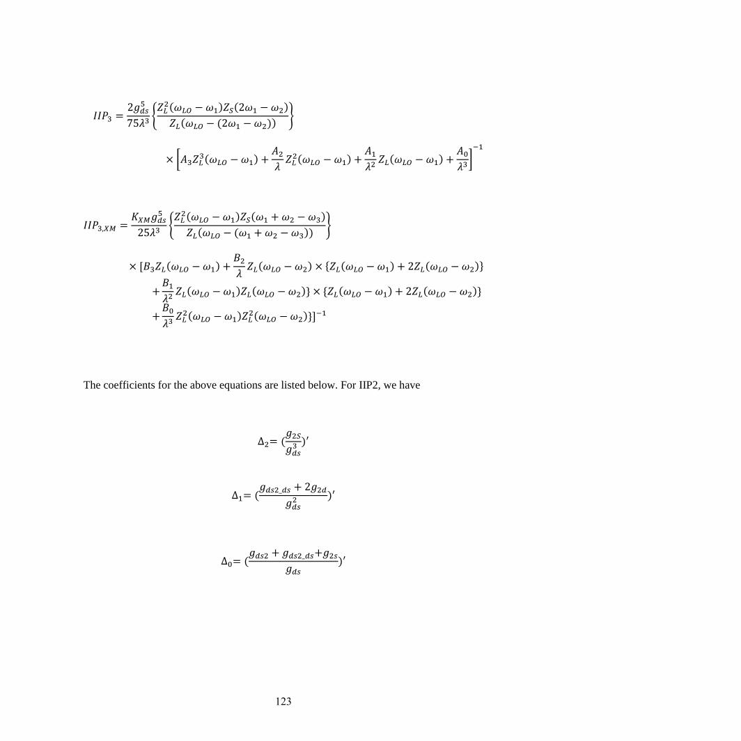
123
[
]
The coefficients for the above equations are listed below. For IIP2, we have
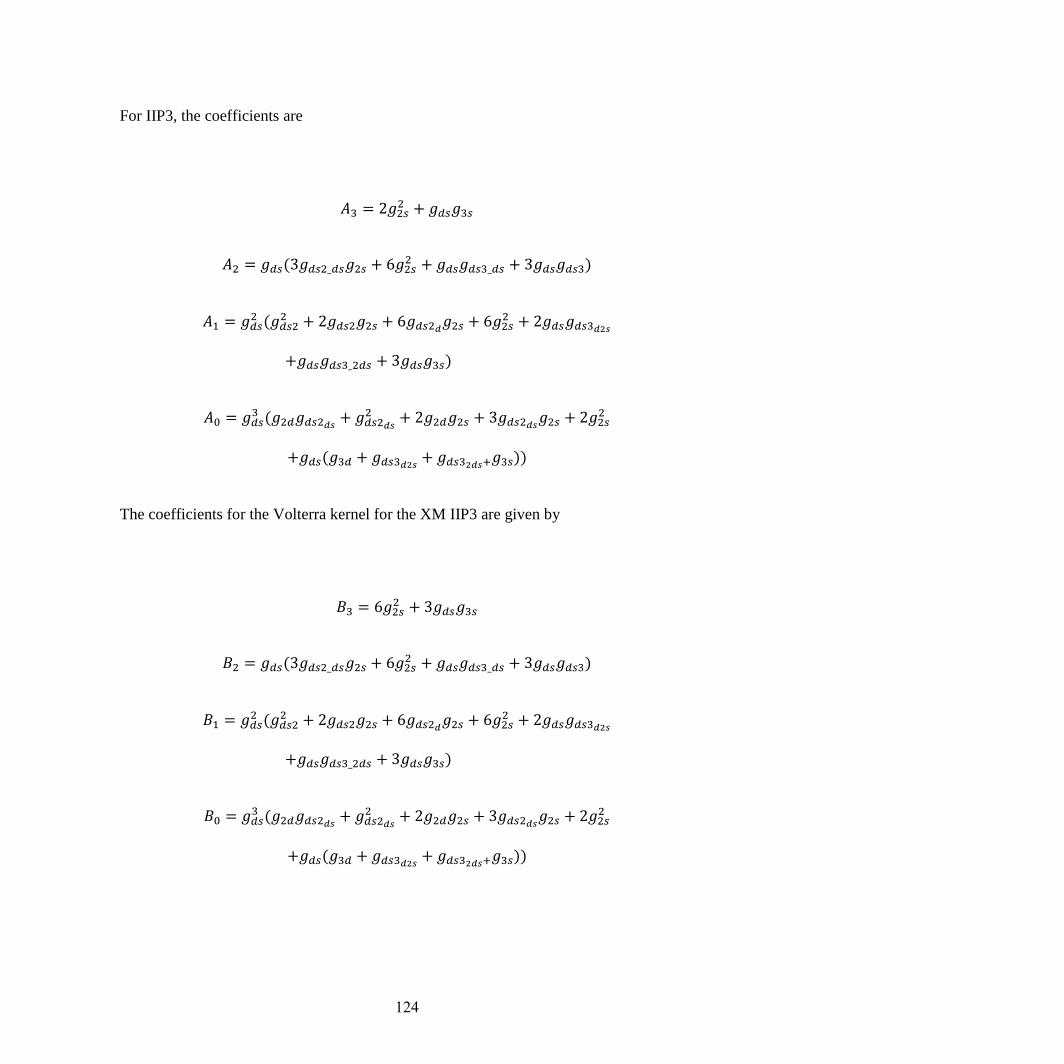
124
For IIP3, the coefficients are
The coefficients for the Volterra kernel for the XM IIP3 are given by
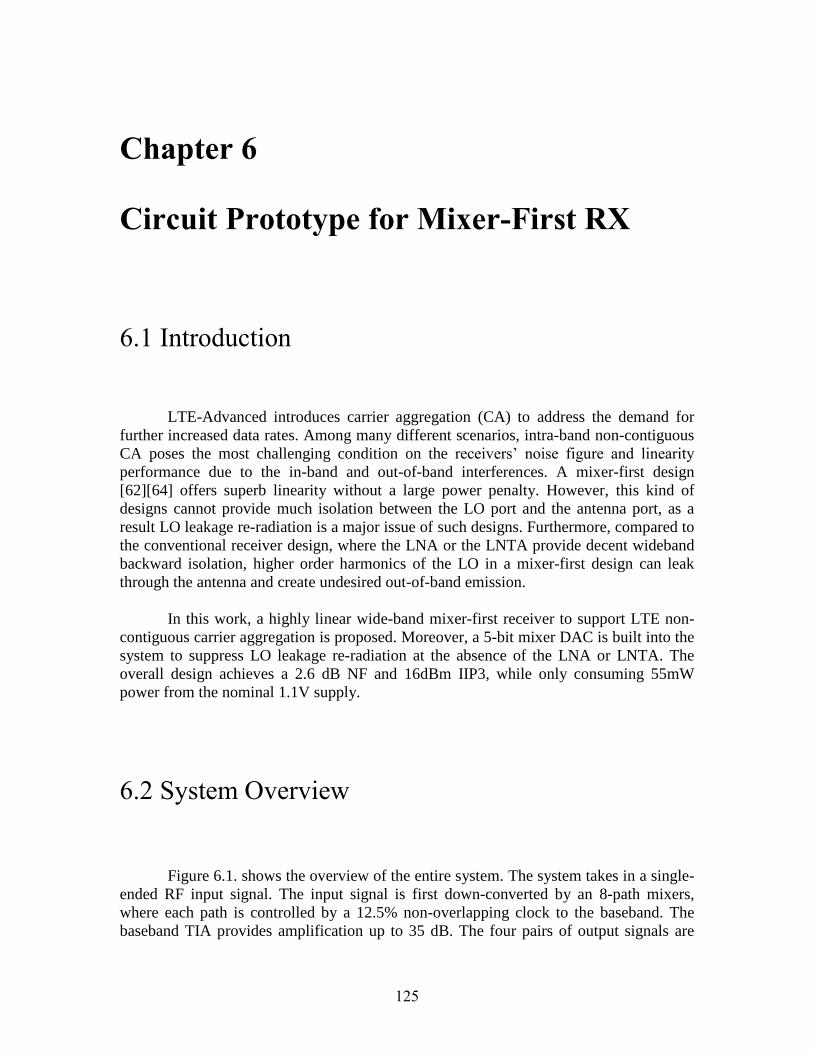
125
Chapter 6
Circuit Prototype for Mixer-First RX
6.1 Introduction
LTE-Advanced introduces carrier aggregation (CA) to address the demand for
further increased data rates. Among many different scenarios, intra-band non-contiguous
CA poses the most challenging condition on the receivers’ noise figure and linearity
performance due to the in-band and out-of-band interferences. A mixer-first design
[62][64] offers superb linearity without a large power penalty. However, this kind of
designs cannot provide much isolation between the LO port and the antenna port, as a
result LO leakage re-radiation is a major issue of such designs. Furthermore, compared to
the conventional receiver design, where the LNA or the LNTA provide decent wideband
backward isolation, higher order harmonics of the LO in a mixer-first design can leak
through the antenna and create undesired out-of-band emission.
In this work, a highly linear wide-band mixer-first receiver to support LTE non-
contiguous carrier aggregation is proposed. Moreover, a 5-bit mixer DAC is built into the
system to suppress LO leakage re-radiation at the absence of the LNA or LNTA. The
overall design achieves a 2.6 dB NF and 16dBm IIP3, while only consuming 55mW
power from the nominal 1.1V supply.
6.2 System Overview
Figure 6.1. shows the overview of the entire system. The system takes in a single-
ended RF input signal. The input signal is first down-converted by an 8-path mixers,
where each path is controlled by a 12.5% non-overlapping clock to the baseband. The
baseband TIA provides amplification up to 35 dB. The four pairs of output signals are
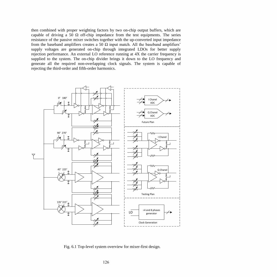
126
then combined with proper weighting factors by two on-chip output buffers, which are
capable of driving a 50 Ω off-chip impedance from the test equipments. The series
resistance of the passive mixer switches together with the up-converted input impedance
from the baseband amplifiers creates a 50 Ω input match. All the baseband amplifiers’
supply voltages are generated on-chip through integrated LDOs for better supply
rejection performance. An external LO reference running at 4X the carrier frequency is
supplied to the system. The on-chip divider brings it down to the LO frequency and
generate all the required non-overlapping clock signals. The system is capable of
rejecting the third-order and fifth-order harmonics.
Fig. 6.1 Top-level system overview for mixer-first design.
0° 180°
90° 270°
45° 225°
135° 315°
I Chanel
Q Chanel
÷4 and 8 phases generatorLO
I ChanelADC
Q ChanelADC
Future Plan
Testing Plan
Clock Generation
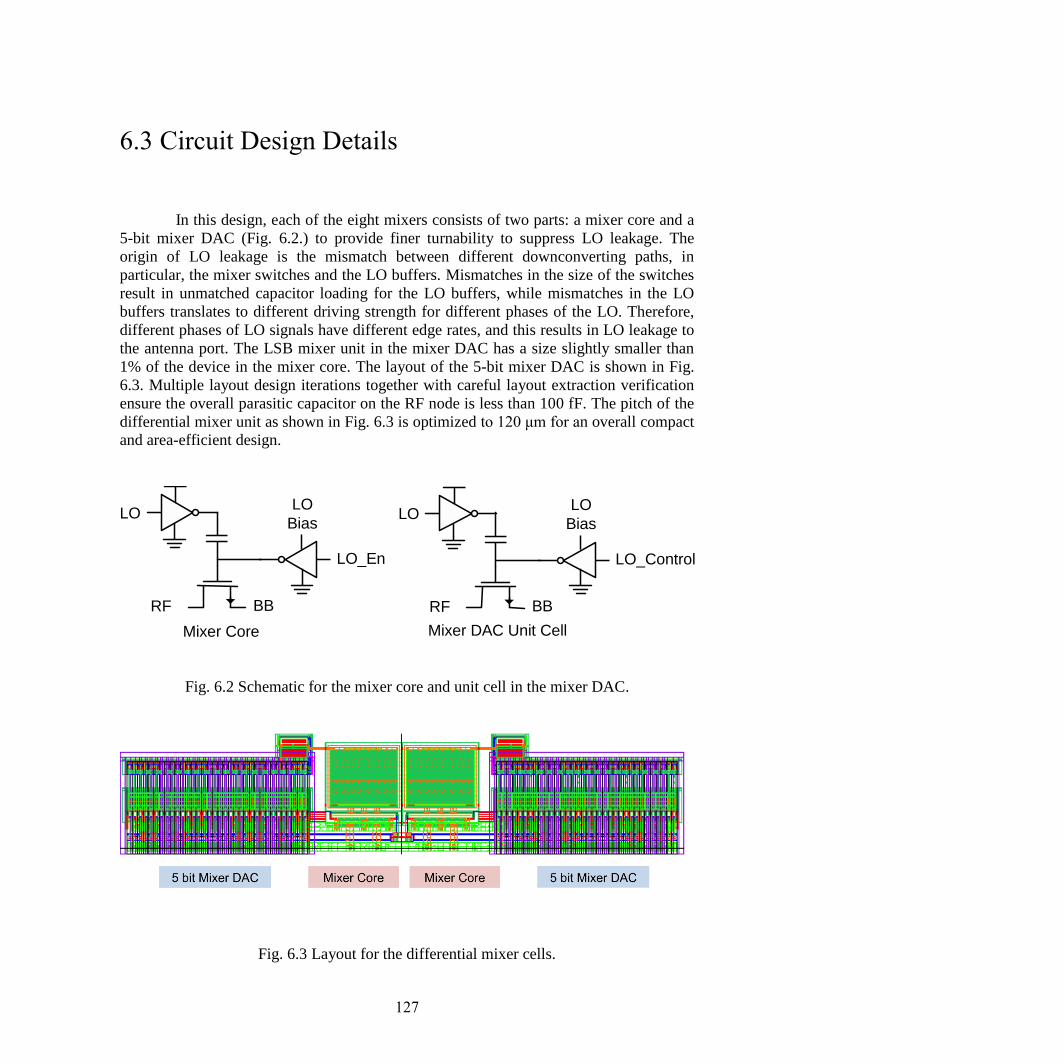
127
6.3 Circuit Design Details
In this design, each of the eight mixers consists of two parts: a mixer core and a
5-bit mixer DAC (Fig. 6.2.) to provide finer turnability to suppress LO leakage. The
origin of LO leakage is the mismatch between different downconverting paths, in
particular, the mixer switches and the LO buffers. Mismatches in the size of the switches
result in unmatched capacitor loading for the LO buffers, while mismatches in the LO
buffers translates to different driving strength for different phases of the LO. Therefore,
different phases of LO signals have different edge rates, and this results in LO leakage to
the antenna port. The LSB mixer unit in the mixer DAC has a size slightly smaller than
1% of the device in the mixer core. The layout of the 5-bit mixer DAC is shown in Fig.
6.3. Multiple layout design iterations together with careful layout extraction verification
ensure the overall parasitic capacitor on the RF node is less than 100 fF. The pitch of the
differential mixer unit as shown in Fig. 6.3 is optimized to 120 μm for an overall compact
and area-efficient design.
Fig. 6.2 Schematic for the mixer core and unit cell in the mixer DAC.
Fig. 6.3 Layout for the differential mixer cells.
LOLO
Bias
RF BB
LO_En
LOLO
Bias
RF BB
LO_Control
Mixer Core Mixer DAC Unit Cell
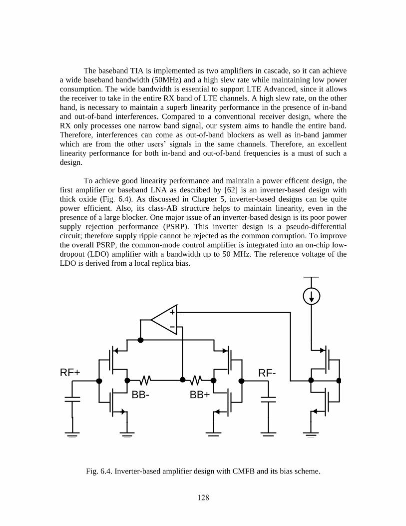
128
The baseband TIA is implemented as two amplifiers in cascade, so it can achieve
a wide baseband bandwidth (50MHz) and a high slew rate while maintaining low power
consumption. The wide bandwidth is essential to support LTE Advanced, since it allows
the receiver to take in the entire RX band of LTE channels. A high slew rate, on the other
hand, is necessary to maintain a superb linearity performance in the presence of in-band
and out-of-band interferences. Compared to a conventional receiver design, where the
RX only processes one narrow band signal, our system aims to handle the entire band.
Therefore, interferences can come as out-of-band blockers as well as in-band jammer
which are from the other users’ signals in the same channels. Therefore, an excellent
linearity performance for both in-band and out-of-band frequencies is a must of such a
design.
To achieve good linearity performance and maintain a power efficent design, the
first amplifier or baseband LNA as described by [62] is an inverter-based design with
thick oxide (Fig. 6.4). As discussed in Chapter 5, inverter-based designs can be quite
power efficient. Also, its class-AB structure helps to maintain linearity, even in the
presence of a large blocker. One major issue of an inverter-based design is its poor power
supply rejection performance (PSRP). This inverter design is a pseudo-differential
circuit; therefore supply ripple cannot be rejected as the common corruption. To improve
the overall PSRP, the common-mode control amplifier is integrated into an on-chip low-
dropout (LDO) amplifier with a bandwidth up to 50 MHz. The reference voltage of the
LDO is derived from a local replica bias.
Fig. 6.4. Inverter-based amplifier design with CMFB and its bias scheme.
RF+ RF-
BB- BB+

129
The second amplifier prefers a high gain and a wide bandwidth for accuracy and
linearity performance. These are quite challenging to achieve for deep sub-micron CMOS
technology, since the supply is limited to 1.1V. Two-stage amplifier design can meet the
gain requirement with ease but the bandwidth and the slew rate performance suffer due to
the size of the compensation capacitors. Moreover, two-stage amplifier design suffers
from a common mode instability issue due to the low supply. Figure 6.5(a)(b) and (c)
demonstrate this issue. Figure 6.5(a) shows a simple two-stage amplifier with Miller
compensation capacitors. The two-stage amplifier is configured with Shunt-Shunt
feedback to function as a trans-impedance amplifier. A common-mode feedback
amplifier detects the output common mode voltage and feeds the control signal back to
the NMOS loads in the first stage to regulate the common-mode bias conditions.
Due to the low supply, only limited headroom can be allocated for the tail current
source, which leads to a poor gds, as shown in Fig. 6.5(b). The issue of headroom
shortage further forces the input pair and the tail current source to operate with small
overdrive voltages, leading to large transistor size. This results in a large parasitic
capacitor connected to the virtual ground node. Large parasitic capacitor on the virtual
ground together with the smaller gds lower the impedance seen by the two input pair
devices. This degrades the common-mode rejection at the first stage of the amplifier as it
increases the common-mode gain of the differential pair. In the two stage amplifier
shown in Fig. 6.5 (a), the two inverted gain stage in series creates an undesired wideband
common-mode positive feedback as shown in Fig. 6.5(b). In the usual case, this
undesired positive loop tends to have a gain less than one, due to the fact that input pair
common-mode gain is heavily degenerated by the tail current source’s output impedance.
However, as discussed above, the first stage common-mode gain in this case is actually
large, and hence the undesired positive feedback would have a strong negative effect on
the overall common-mode stability.
In general, the desirable built-in common-mode control loop, as shown in Fig.
6.5(b) tends to be narrow band due to reasons explained in [73]. Therefore, in low
frequency, where the desired negative common-mode loop is still strong, the common-
mode signal is well-regulated. However, the undesired positive feedback will take over
beyond unity gain frequency of the common-mode loop, where the desired negative
common-mode loop begins to fade away as shown in Fig. 6.5(c). As a result, the phase
margin of the common-mode loop degrades significantly. In summary, it is difficult to
realize a robust two-stage amplifier design over processes and corners in a deep sub-
micron CMOS technology due to the limited supply headroom.
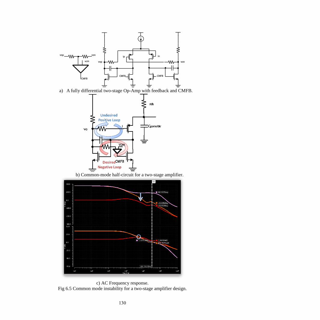
130
a) A fully differential two-stage Op-Amp with feedback and CMFB.
b) Common-mode half-circuit for a two-stage amplifier.
c) AC Frequency response.
Fig 6.5 Common mode instability for a two-stage amplifier design.
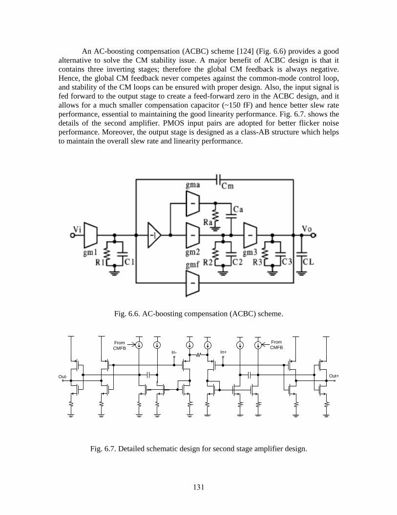
131
An AC-boosting compensation (ACBC) scheme [124] (Fig. 6.6) provides a good
alternative to solve the CM stability issue. A major benefit of ACBC design is that it
contains three inverting stages; therefore the global CM feedback is always negative.
Hence, the global CM feedback never competes against the common-mode control loop,
and stability of the CM loops can be ensured with proper design. Also, the input signal is
fed forward to the output stage to create a feed-forward zero in the ACBC design, and it
allows for a much smaller compensation capacitor (~150 fF) and hence better slew rate
performance, essential to maintaining the good linearity performance. Fig. 6.7. shows the
details of the second amplifier. PMOS input pairs are adopted for better flicker noise
performance. Moreover, the output stage is designed as a class-AB structure which helps
to maintain the overall slew rate and linearity performance.
Fig. 6.6. AC-boosting compensation (ACBC) scheme.
Fig. 6.7. Detailed schematic design for second stage amplifier design.
Out- Out+
In- In+
From
CMFB
From
CMFB
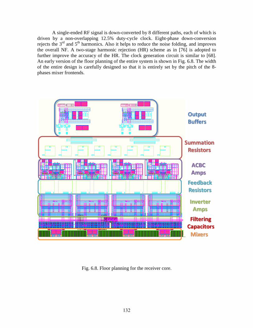
132
A single-ended RF signal is down-converted by 8 different paths, each of which is
driven by a non-overlapping 12.5% duty-cycle clock. Eight-phase down-conversion
rejects the 3rd
and 5th
harmonics. Also it helps to reduce the noise folding, and improves
the overall NF. A two-stage harmonic rejection (HR) scheme as in [76] is adopted to
further improve the accuracy of the HR. The clock generation circuit is similar to [68].
An early version of the floor planning of the entire system is shown in Fig. 6.8. The width
of the entire design is carefully designed so that it is entirely set by the pitch of the 8-
phases mixer frontends.
Fig. 6.8. Floor planning for the receiver core.
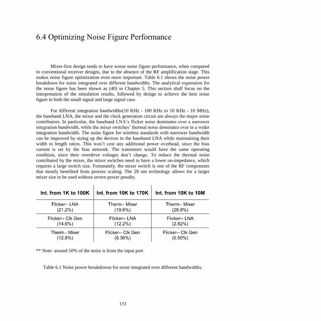
133
6.4 Optimizing Noise Figure Performance
Mixer-first design tends to have worse noise figure performance, when compared
to conventional receiver designs, due to the absence of the RF amplification stage. This
makes noise figure optimization even more important. Table 6.1 shows the noise power
breakdown for noise integrated over different bandwidths. The analytical expression for
the noise figure has been shown as (40) in Chapter 5. This section shall focus on the
interpretation of the simulation results, followed by design to achieve the best noise
figure in both the small signal and large signal case.
For different integration bandwidths(10 KHz - 100 KHz to 10 KHz - 10 MHz),
the baseband LNA, the mixer and the clock generation circuit are always the major noise
contributors. In particular, the baseband LNA’s flicker noise dominates over a narrower
integration bandwidth, while the mixer switches’ thermal noise dominates over in a wider
integration bandwidth. The noise figure for wireless standards with narrower bandwidth
can be improved by sizing up the devices in the baseband LNA while maintaining their
width to length ratios. This won’t cost any additional power overhead, since the bias
current is set by the bias network. The transistors would have the same operating
condition, since their overdrive voltages don’t change. To reduce the thermal noise
contributed by the mixer, the mixer switches need to have a lower on-impedance, which
requires a large switch size. Fortunately, the mixer switch is one of the RF components
that mostly benefited from process scaling. The 28 nm technology allows for a larger
mixer size to be used without severe power penalty.
** Note: around 50% of the noise is from the input port
Table 6.1 Noise power breakdowns for noise integrated over different bandwidths.
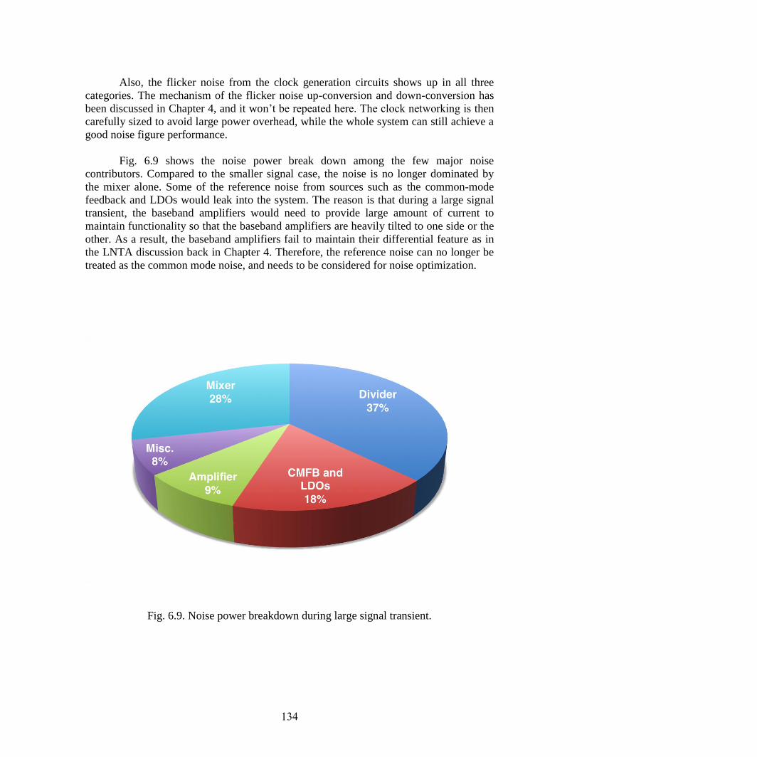
134
Also, the flicker noise from the clock generation circuits shows up in all three
categories. The mechanism of the flicker noise up-conversion and down-conversion has
been discussed in Chapter 4, and it won’t be repeated here. The clock networking is then
carefully sized to avoid large power overhead, while the whole system can still achieve a
good noise figure performance.
Fig. 6.9 shows the noise power break down among the few major noise
contributors. Compared to the smaller signal case, the noise is no longer dominated by
the mixer alone. Some of the reference noise from sources such as the common-mode
feedback and LDOs would leak into the system. The reason is that during a large signal
transient, the baseband amplifiers would need to provide large amount of current to
maintain functionality so that the baseband amplifiers are heavily tilted to one side or the
other. As a result, the baseband amplifiers fail to maintain their differential feature as in
the LNTA discussion back in Chapter 4. Therefore, the reference noise can no longer be
treated as the common mode noise, and needs to be considered for noise optimization.
Fig. 6.9. Noise power breakdown during large signal transient.
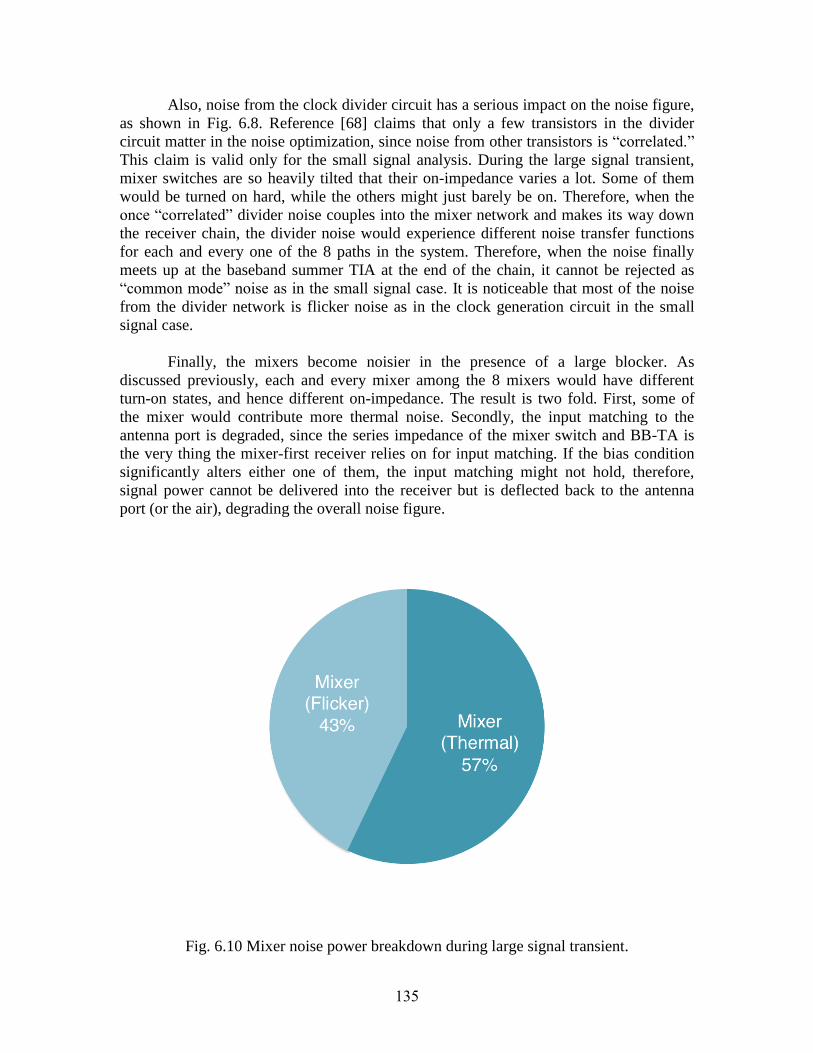
135
Also, noise from the clock divider circuit has a serious impact on the noise figure,
as shown in Fig. 6.8. Reference [68] claims that only a few transistors in the divider
circuit matter in the noise optimization, since noise from other transistors is “correlated.”
This claim is valid only for the small signal analysis. During the large signal transient,
mixer switches are so heavily tilted that their on-impedance varies a lot. Some of them
would be turned on hard, while the others might just barely be on. Therefore, when the
once “correlated” divider noise couples into the mixer network and makes its way down
the receiver chain, the divider noise would experience different noise transfer functions
for each and every one of the 8 paths in the system. Therefore, when the noise finally
meets up at the baseband summer TIA at the end of the chain, it cannot be rejected as
“common mode” noise as in the small signal case. It is noticeable that most of the noise
from the divider network is flicker noise as in the clock generation circuit in the small
signal case.
Finally, the mixers become noisier in the presence of a large blocker. As
discussed previously, each and every mixer among the 8 mixers would have different
turn-on states, and hence different on-impedance. The result is two fold. First, some of
the mixer would contribute more thermal noise. Secondly, the input matching to the
antenna port is degraded, since the series impedance of the mixer switch and BB-TA is
the very thing the mixer-first receiver relies on for input matching. If the bias condition
significantly alters either one of them, the input matching might not hold, therefore,
signal power cannot be delivered into the receiver but is deflected back to the antenna
port (or the air), degrading the overall noise figure.
Fig. 6.10 Mixer noise power breakdown during large signal transient.
136
Fig. 6.10 demonstrates one important point in optimizing the mixer for large
signal transient in a receiver like this. More than 40% of the noise from the mixers is
flicker noise, which is not present at all in the small signal case. It has been established
back in Chapter 5 that passive mixers doesn’t require a DC-bias current, and hence they
are free of flicker noise. These seemingly contradictory simulation results might cause
some confusion to arise. In the small signal case, the input signal is so small that it
doesn’t disrupt the normal biasing condition of the entire system. Hence, the mixer
transistors don’t generate any flicker noise. During the large signal transient, the receiver
is so heavily tilted to one direction or the other that there will indeed be a DC current
passing through the mixers when the switches are turned on. Therefore, optimizing the
mixers’ flicker noise performance is as important as optimizing their thermal noise
number for a mixer-first receiver design.
6.5 Measurement Results
The chip is sponsored by the Intel Corporation and fabricated by TSMC. The
design is implemented in a general-purpose high-k metal gate 28nm technology with
1.1V nominal supply voltage. The chip micro-photograph is shown in Fig. 6.11. The core
area of the design is 460 μm by 500 μm. This includes the 8 paths of passive mixer cells
(each contains a mixer core and a 5-bit mixer DAC), four channels of baseband
amplification stages, a clock generation circuit for the 8 phases of non-overlapping LO
signals, all the local LDOs for the first and second stage of amplifiers together with the
digital control unit. The local LDOs are implemented with 1.8V thick-oxide transistors,
and they are connected to the high supply voltage. They are designed with the intention to
operate over a wide range of supply voltages (1.5V-1.9V).
For testing purpose, two baseband output buffers are also integrated onto the same
silicon, They are powered with a high supply voltage (1.5 V – 2 V). These two output
buffers are capable of driving an off-chip 50 Ω impedance presented by the test
equipment, which greatly reduces the complexity of testing.

137
Fig. 6.11 Chip Microphotograph.
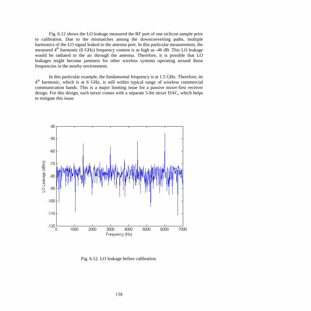
138
Fig. 6.12 shows the LO leakage measured the RF port of one siclicon sample prior
to calibration. Due to the mismatches among the downconverting paths, multiple
harmonics of the LO signal leaked to the antenna port. In this particular measurement, the
measured 4th
harmonic (6 GHz) frequency content is as high as -46 dB. This LO leakage
would be radiated to the air through the antenna. Therefore, it is possible that LO
leakages might become jammers for other wireless systems operating around those
frequencies in the nearby environment.
In this particular example, the fundamental frequency is at 1.5 GHz. Therefore, its
4th
harmonic, which is at 6 GHz, is still within typical range of wireless commercial
communication bands. This is a major limiting issue for a passive mixer-first receiver
design. For this design, each mixer comes with a separate 5-bit mixer DAC, which helps
to mitigate this issue.
Fig. 6.12. LO leakage before calibration.
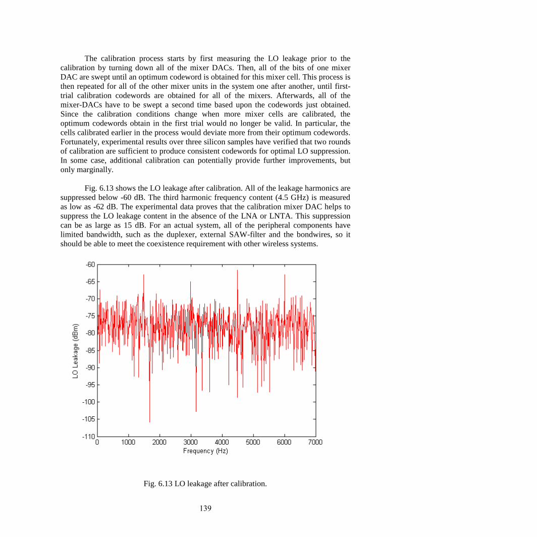
139
The calibration process starts by first measuring the LO leakage prior to the
calibration by turning down all of the mixer DACs. Then, all of the bits of one mixer
DAC are swept until an optimum codeword is obtained for this mixer cell. This process is
then repeated for all of the other mixer units in the system one after another, until first-
trial calibration codewords are obtained for all of the mixers. Afterwards, all of the
mixer-DACs have to be swept a second time based upon the codewords just obtained.
Since the calibration conditions change when more mixer cells are calibrated, the
optimum codewords obtain in the first trial would no longer be valid. In particular, the
cells calibrated earlier in the process would deviate more from their optimum codewords.
Fortunately, experimental results over three silicon samples have verified that two rounds
of calibration are sufficient to produce consistent codewords for optimal LO suppression.
In some case, additional calibration can potentially provide further improvements, but
only marginally.
Fig. 6.13 shows the LO leakage after calibration. All of the leakage harmonics are
suppressed below -60 dB. The third harmonic frequency content (4.5 GHz) is measured
as low as -62 dB. The experimental data proves that the calibration mixer DAC helps to
suppress the LO leakage content in the absence of the LNA or LNTA. This suppression
can be as large as 15 dB. For an actual system, all of the peripheral components have
limited bandwidth, such as the duplexer, external SAW-filter and the bondwires, so it
should be able to meet the coexistence requirement with other wireless systems.
Fig. 6.13 LO leakage after calibration.
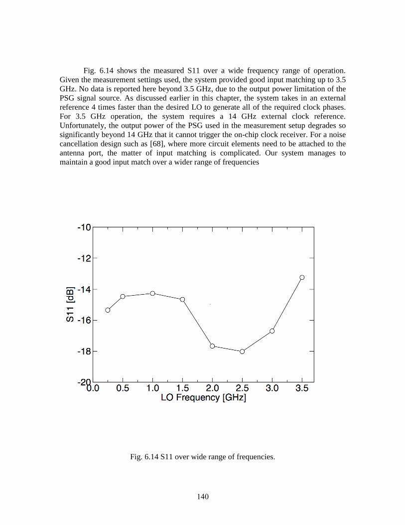
140
Fig. 6.14 shows the measured S11 over a wide frequency range of operation.
Given the measurement settings used, the system provided good input matching up to 3.5
GHz. No data is reported here beyond 3.5 GHz, due to the output power limitation of the
PSG signal source. As discussed earlier in this chapter, the system takes in an external
reference 4 times faster than the desired LO to generate all of the required clock phases.
For 3.5 GHz operation, the system requires a 14 GHz external clock reference.
Unfortunately, the output power of the PSG used in the measurement setup degrades so
significantly beyond 14 GHz that it cannot trigger the on-chip clock receiver. For a noise
cancellation design such as [68], where more circuit elements need to be attached to the
antenna port, the matter of input matching is complicated. Our system manages to
maintain a good input match over a wider range of frequencies
Fig. 6.14 S11 over wide range of frequencies.
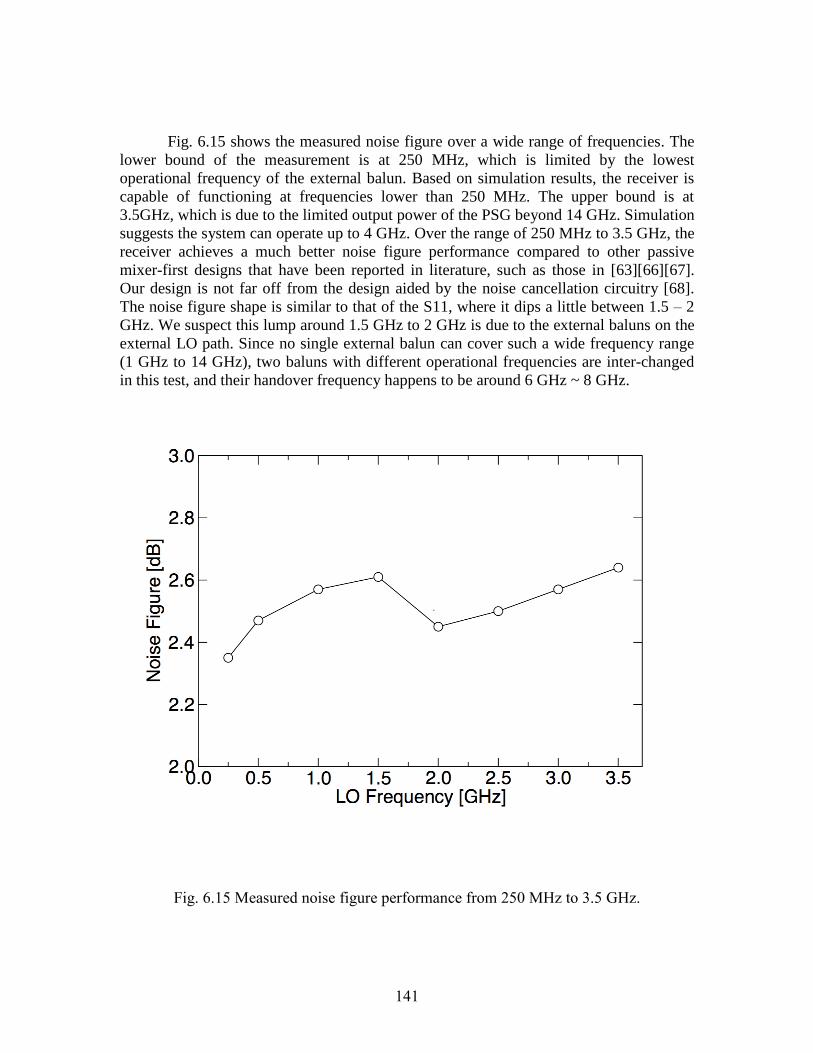
141
Fig. 6.15 shows the measured noise figure over a wide range of frequencies. The
lower bound of the measurement is at 250 MHz, which is limited by the lowest
operational frequency of the external balun. Based on simulation results, the receiver is
capable of functioning at frequencies lower than 250 MHz. The upper bound is at
3.5GHz, which is due to the limited output power of the PSG beyond 14 GHz. Simulation
suggests the system can operate up to 4 GHz. Over the range of 250 MHz to 3.5 GHz, the
receiver achieves a much better noise figure performance compared to other passive
mixer-first designs that have been reported in literature, such as those in [63][66][67].
Our design is not far off from the design aided by the noise cancellation circuitry [68].
The noise figure shape is similar to that of the S11, where it dips a little between 1.5 – 2
GHz. We suspect this lump around 1.5 GHz to 2 GHz is due to the external baluns on the
external LO path. Since no single external balun can cover such a wide frequency range
(1 GHz to 14 GHz), two baluns with different operational frequencies are inter-changed
in this test, and their handover frequency happens to be around 6 GHz ~ 8 GHz.
Fig. 6.15 Measured noise figure performance from 250 MHz to 3.5 GHz.
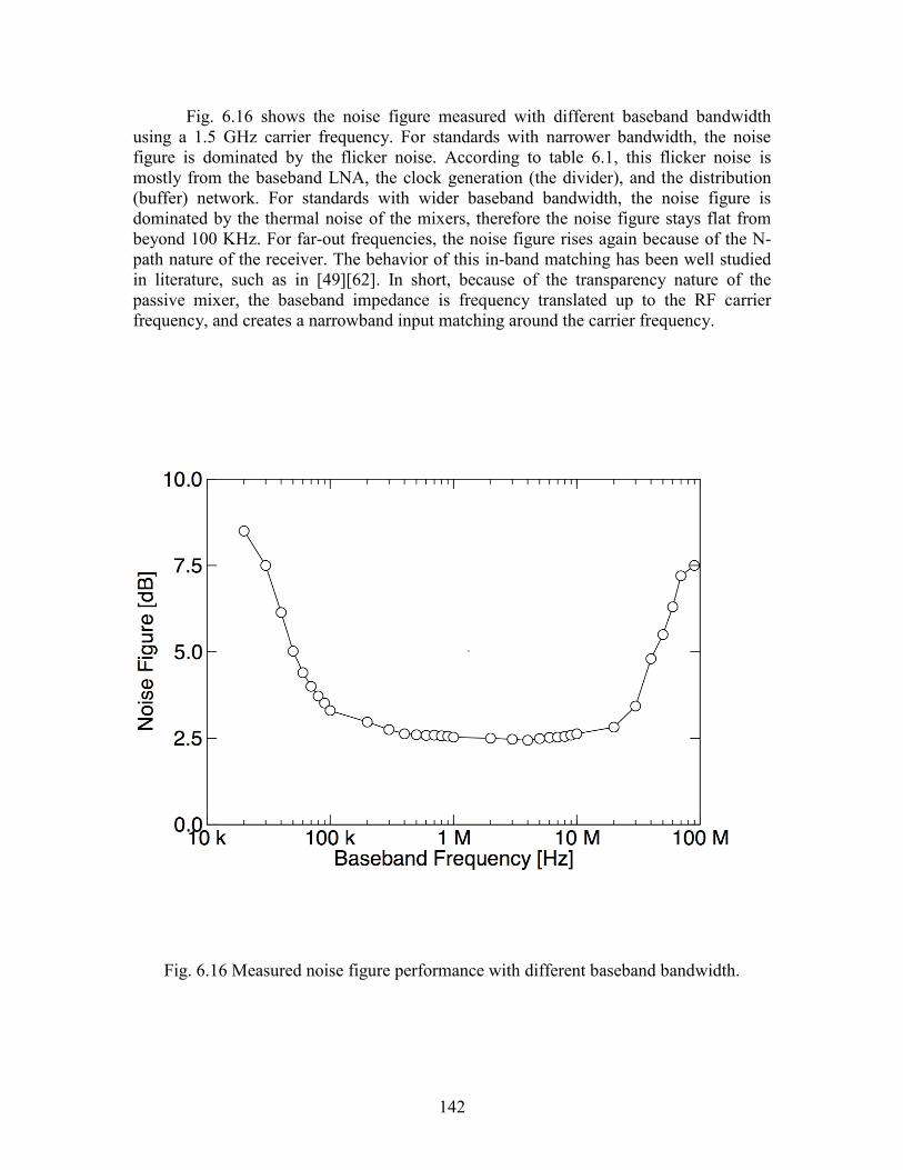
142
Fig. 6.16 shows the noise figure measured with different baseband bandwidth
using a 1.5 GHz carrier frequency. For standards with narrower bandwidth, the noise
figure is dominated by the flicker noise. According to table 6.1, this flicker noise is
mostly from the baseband LNA, the clock generation (the divider), and the distribution
(buffer) network. For standards with wider baseband bandwidth, the noise figure is
dominated by the thermal noise of the mixers, therefore the noise figure stays flat from
beyond 100 KHz. For far-out frequencies, the noise figure rises again because of the N-
path nature of the receiver. The behavior of this in-band matching has been well studied
in literature, such as in [49][62]. In short, because of the transparency nature of the
passive mixer, the baseband impedance is frequency translated up to the RF carrier
frequency, and creates a narrowband input matching around the carrier frequency.
Fig. 6.16 Measured noise figure performance with different baseband bandwidth.
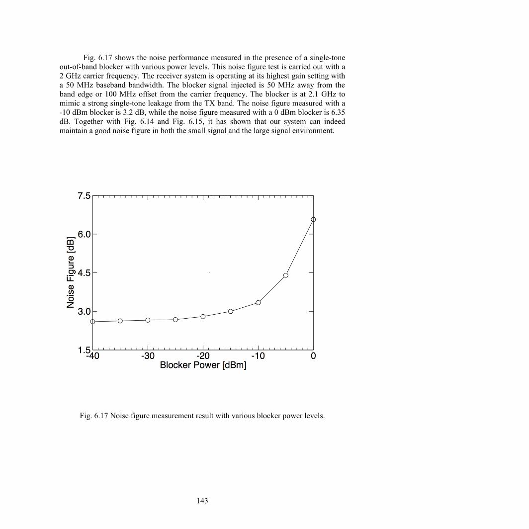
143
Fig. 6.17 shows the noise performance measured in the presence of a single-tone
out-of-band blocker with various power levels. This noise figure test is carried out with a
2 GHz carrier frequency. The receiver system is operating at its highest gain setting with
a 50 MHz baseband bandwidth. The blocker signal injected is 50 MHz away from the
band edge or 100 MHz offset from the carrier frequency. The blocker is at 2.1 GHz to
mimic a strong single-tone leakage from the TX band. The noise figure measured with a
-10 dBm blocker is 3.2 dB, while the noise figure measured with a 0 dBm blocker is 6.35
dB. Together with Fig. 6.14 and Fig. 6.15, it has shown that our system can indeed
maintain a good noise figure in both the small signal and the large signal environment.
Fig. 6.17 Noise figure measurement result with various blocker power levels.
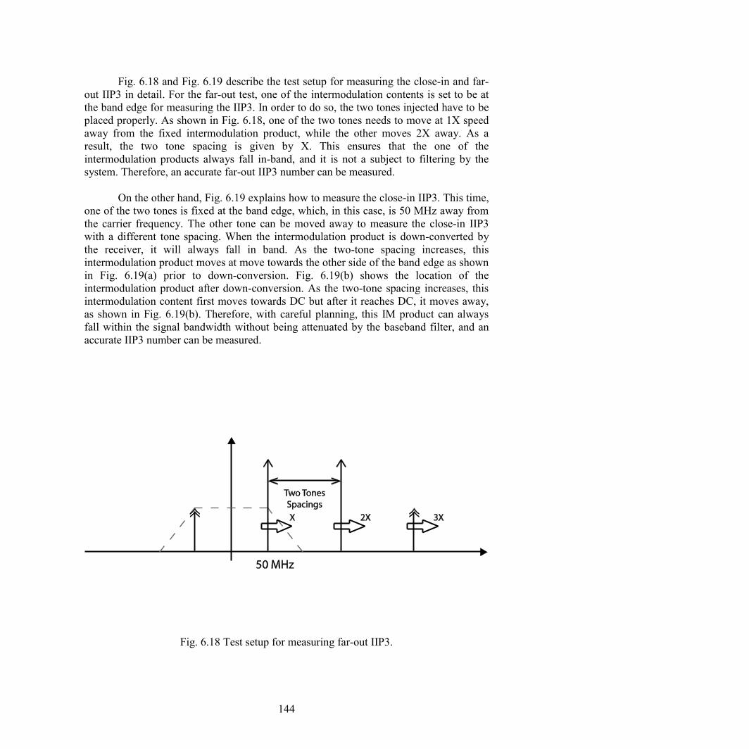
144
Fig. 6.18 and Fig. 6.19 describe the test setup for measuring the close-in and far-
out IIP3 in detail. For the far-out test, one of the intermodulation contents is set to be at
the band edge for measuring the IIP3. In order to do so, the two tones injected have to be
placed properly. As shown in Fig. 6.18, one of the two tones needs to move at 1X speed
away from the fixed intermodulation product, while the other moves 2X away. As a
result, the two tone spacing is given by X. This ensures that the one of the
intermodulation products always fall in-band, and it is not a subject to filtering by the
system. Therefore, an accurate far-out IIP3 number can be measured.
On the other hand, Fig. 6.19 explains how to measure the close-in IIP3. This time,
one of the two tones is fixed at the band edge, which, in this case, is 50 MHz away from
the carrier frequency. The other tone can be moved away to measure the close-in IIP3
with a different tone spacing. When the intermodulation product is down-converted by
the receiver, it will always fall in band. As the two-tone spacing increases, this
intermodulation product moves at move towards the other side of the band edge as shown
in Fig. 6.19(a) prior to down-conversion. Fig. 6.19(b) shows the location of the
intermodulation product after down-conversion. As the two-tone spacing increases, this
intermodulation content first moves towards DC but after it reaches DC, it moves away,
as shown in Fig. 6.19(b). Therefore, with careful planning, this IM product can always
fall within the signal bandwidth without being attenuated by the baseband filter, and an
accurate IIP3 number can be measured.
Fig. 6.18 Test setup for measuring far-out IIP3.
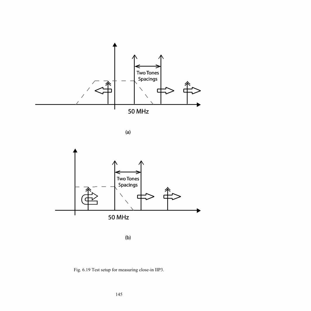
145
Fig. 6.19 Test setup for measuring close-in IIP3.

146
Fig. 6.20 shows the measured IIP3 from close-in and far-out tests around a 2 GHz
carrier frequency. The white dots are data points collected from the close-in test, while
the black points are from the far-out test. The receiver achieves a > +6.4 dBm IIP3 within
the 3dB corner frequency consistently. Moreover, the system achieves an out-of-band
IIP3 as high as +20.5 dBm with a 250 MHz tone spacing. The IIP3 measured with a 50
MHz tone spacing (one tone at 2.05GHz, while the other sits at 2.10 GHz) is +15.4 dBm.
This is for the test case where the close-in TX leakage could degrade the receiver’s
performance. The IIP3 is flat close-in, since the linearity is mostly dominated by the
baseband amplifiers’ linearity performance. As the two tone spacing increases, the IIP3
improves since one of the tones is moving out of band. Eventually, the IIP3 saturates,
since the linearity at that point is limited by performance of the intrinsic mixer switches.
Fig. 6.20 In-band and out-of-band IIP3 measured.
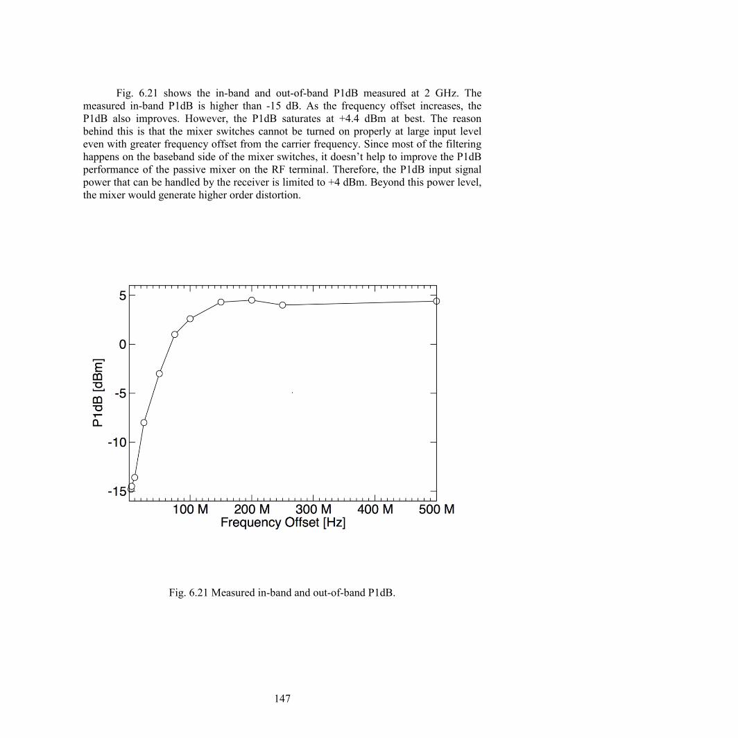
147
Fig. 6.21 shows the in-band and out-of-band P1dB measured at 2 GHz. The
measured in-band P1dB is higher than -15 dB. As the frequency offset increases, the
P1dB also improves. However, the P1dB saturates at +4.4 dBm at best. The reason
behind this is that the mixer switches cannot be turned on properly at large input level
even with greater frequency offset from the carrier frequency. Since most of the filtering
happens on the baseband side of the mixer switches, it doesn’t help to improve the P1dB
performance of the passive mixer on the RF terminal. Therefore, the P1dB input signal
power that can be handled by the receiver is limited to +4 dBm. Beyond this power level,
the mixer would generate higher order distortion.
Fig. 6.21 Measured in-band and out-of-band P1dB.
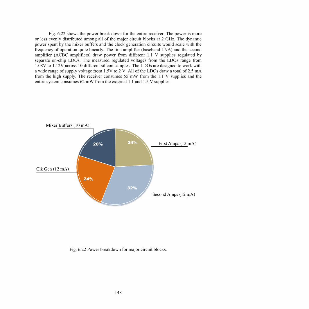
148
Fig. 6.22 shows the power break down for the entire receiver. The power is more
or less evenly distributed among all of the major circuit blocks at 2 GHz. The dynamic
power spent by the mixer buffers and the clock generation circuits would scale with the
frequency of operation quite linearly. The first amplifier (baseband LNA) and the second
amplifier (ACBC amplifiers) draw power from different 1.1 V supplies regulated by
separate on-chip LDOs. The measured regulated voltages from the LDOs range from
1.08V to 1.12V across 10 different silicon samples. The LDOs are designed to work with
a wide range of supply voltage from 1.5V to 2 V. All of the LDOs draw a total of 2.5 mA
from the high supply. The receiver consumes 55 mW from the 1.1 V supplies and the
entire system consumes 62 mW from the external 1.1 and 1.5 V supplies.
Fig. 6.22 Power breakdown for major circuit blocks.

149
Table 6.2 compares our work with other state-of-the-art receivers implemented in
different architectures. Compared to the other mixer-first receiver designs, our system
manages to achieve the widest frequency range, benefiting from the 28 nm technology.
Compared to the other state-of-the-art research, our system achieves the widest baseband
bandwidth. Also, it maintains a competitive IIP3 performance if it is not better than the
others. Even compared to the design with noise cancellation [68], our work is not far off:
the measured small signal noise figure is around 2.5 dB while the noise cancellation
design can achieve a sub 2 dB noise figure. Moreover, the measured noise figure with an
out-of-band 0 dBm blocker present is 6.4 dB including the noise contributed by the five
LDOs, compared with 4.1 dB for a design with noise cancellation. On the other hand, our
design with integrated LDOs still takes less than half of the area, and consumes less
power compared to [68].
Compared to recent research works for the LTE-A standards, our work manages
to cover a wide frequency range of operation. It achieves a better noise figure, and it is
more linear within the signal bandwidth and out of the signal bandwidth. Also, it achieves
a footprint that is far smaller than existing designs, and consumes much less power.
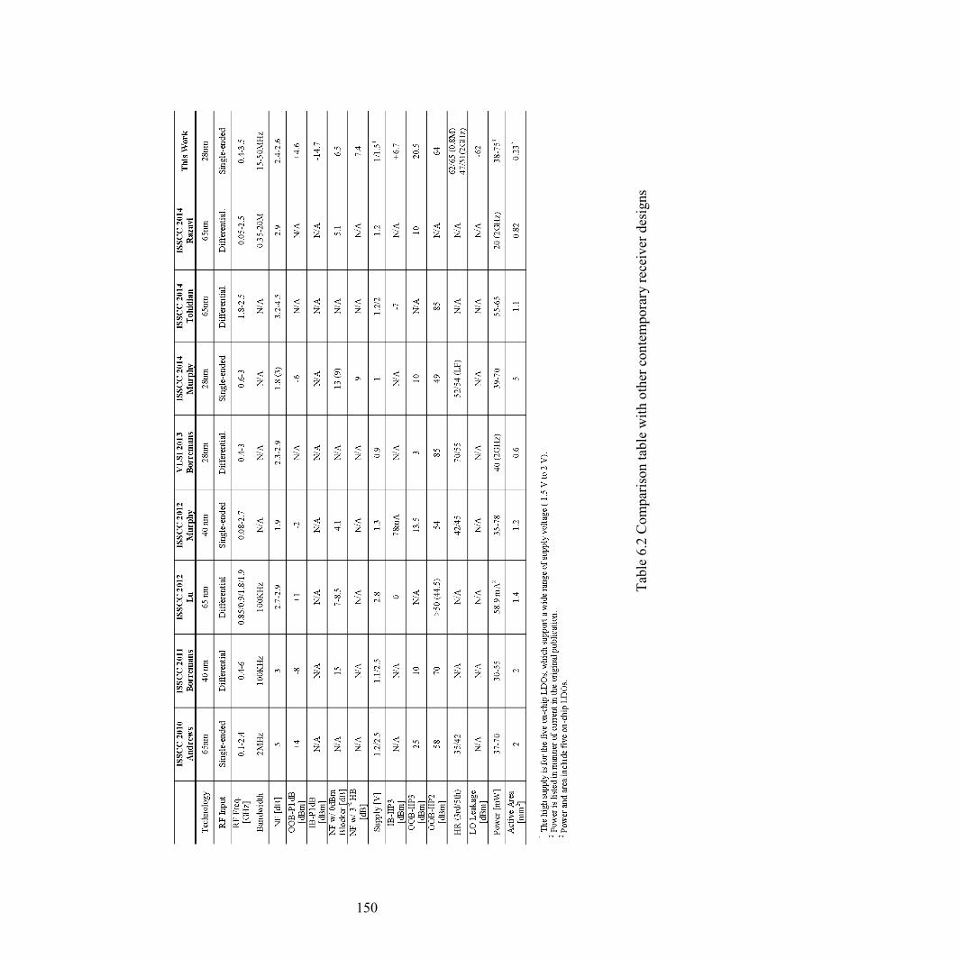
150
Tab
le 6
.2 C
om
par
ison t
able
wit
h o
ther
conte
mpora
ry r
ecei
ver
des
igns
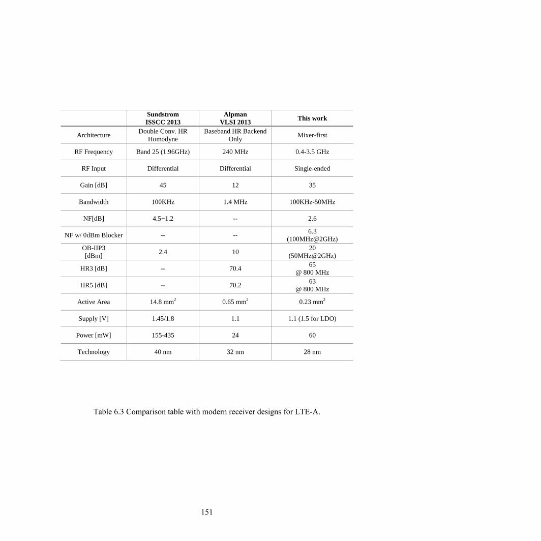
151
Sundstrom
ISSCC 2013
Alpman
VLSI 2013 This work
Architecture Double Conv. HR
Homodyne
Baseband HR Backend
Only Mixer-first
RF Frequency Band 25 (1.96GHz) 240 MHz 0.4-3.5 GHz
RF Input Differential Differential Single-ended
Gain [dB] 45 12 35
Bandwidth 100KHz 1.4 MHz 100KHz-50MHz
NF[dB] 4.5+1.2 -- 2.6
NF w/ 0dBm Blocker -- -- 6.3
(100MHz@2GHz)
OB-IIP3
[dBm] 2.4 10
20
(50MHz@2GHz)
HR3 [dB] -- 70.4 65
@ 800 MHz
HR5 [dB] -- 70.2 63
@ 800 MHz
Active Area 14.8 mm2 0.65 mm
2 0.23 mm
2
Supply [V] 1.45/1.8 1.1 1.1 (1.5 for LDO)
Power [mW] 155-435 24 60
Technology 40 nm 32 nm 28 nm
Table 6.3 Comparison table with modern receiver designs for LTE-A.
152
6.6 Summary
A passive-mixer-first receiver designed in 28 nm CMOS is presented in this
chapter, where the frontend 5-bit mixer-DAC provides a wide-band tunable impedance
match to suppress the LO leakage. The baseband LNA together with the AC-boosting
compensation amplifier provides a 50MHz baseband bandwidth. This provides power-
efficient support for non-contiguous carrier aggregation in LTE. The circuit achieves
<3dB NF, >15dBm IIP3 and 35dB gain with 55mW power.
153
Chapter 7
Conclusion
In this work, we demonstrated two receiver designs to address two different aspects
of future wireless standards. First off, an experimental prototype ADC based receiver
design is presented as a direct RF-to-digital converter for software defined radio
application. The large difference between the baseband bandwidth and the carrier
frequency provide the large oversampling ratio necessary to avoid noise folding. The
noise shaping feature provided by the ΔΣ modulator supplies a high-resolution
conversion only in the frequency range of interest such that the desired high-speed and
high-resolution conversion can be carried out in a power efficient manner. The integrated
CMIS mixer performs the frequency translation in a simple yet elegant manner, which
allows the mixer to be easily implemented and better integrated for such a design.
The prototype design supports a frequency of operation from 400 MHz to 4000
MHz, which covers all LTE bands worldwide. An NRZ feedback DAC design reduces
the jitter sensitivity of the system, and aids in achieving a high SNDR over the frequency
range of interest. It provides a large dynamic range with low power consumption. It
meets the three major criteria of SDR systems. Without any bulky passives, the design
maintains a small footprint, while a digitally-oriented design methodology enables a truly
flexible receiver that is able to adapt to different standards with the change of a few
control bits. Finally, the solution can scale naturally with technology.
The second design addresses the challenges presented by carrier aggregation
where a passive-mixer-first receiver design is proposed. Avoiding the front-end gain
element, such as an LNA or LNTA, the mixer and the baseband circuits only need to
process a small signal swing, which helps to maintain the overall linearity. This superb
linearity performance makes such a design a perfect candidate for applications like LTE
Advanced, where the interferences can come within or out of the receiver bands. The
wide-band tunable mixer DAC helps to suppress the LO leakage due to the absence of
any reverse isolation of the front end. Moreover, careful noise analysis for both the small
signal case and the large signal case allows the receiver to achieve a competitive noise
figure compared to conventional designs even with at the absence of the RF gain stage.
An experimental prototype implemented in 28 nm CMOS is presented, where the
frontend 5-bit mixer-DAC provides a wide-band tunable impedance match to suppress
the LO leakage. The baseband LNA and the AC-boosting compensation amplifier
provide a 50MHz baseband bandwidth, which provides support for non-contiguous
carrier aggregation for LTE in power efficient manners. The circuit achieves <3dB NF,
>15dBm IIP3 and 35dB gain with 55mW power.

154
7.1 Significant Contributions
The key accomplishments of this research are:
Designed a direct RF to digital ΔΣ converter supporting over a decade of
operating frequencies (400 MHz to 4 GHz), which is better than any related work
(such as band-pass ΔΣ, RF-ADC or ΔΣ down-converter) reported until now.
Proposed and implemented a novel feedback DAC switching scheme to alleviate
the impact of clock jitter for a multi-gigahertz ΔΣ modulator design.
Designed a novel low-power highly linear class-AB low-noise trans-conductance
amplifier (LNTA) with wide-band input matching.
Conducted both analytical and numerical analysis on the high-speed ΔΣ
modulator jitter sensitivity issue, and verified the result with actual silicon
samples.
Proposed and verified techniques effectively mitigating the jitter sensitivity issue
for a high-speed ΔΣ modulator design.
Designed a highly linear passive mixer-first receiver with up to 50 MHz baseband
bandwidth with integrated LDO design.
Proposed and designed a 5-bit mixer calibration DAC for LO leakage suppression.
7.1 Future Work
We suggest several directions for futher research and improvement of our work:
Improving the operational fequency of the current ΔΣ converter by re-designing
the comparator with a two-way time-interleaved design, which is common in
high-speed serializer and de-serializer designs.
Increasing the front-end gain in the ΔΣ converter design to achieve a better noise
155
figure for the overall system.
An implementation of noise cancelling circuits around the mixer-first design to
achieve an even better noise figure performance.
Attempting a different TX signal injection point the into the mixer-first design to
achieve better TX resilience.
Developing a calibration algorithm for LO leakage suppression.
Combining the ΔΣ converter and the passive-mixer’s transparency property to
achieve a design that is capable of direct down-conversion, while still being
resilient to large blockers, as shown in Fig. 7.1.
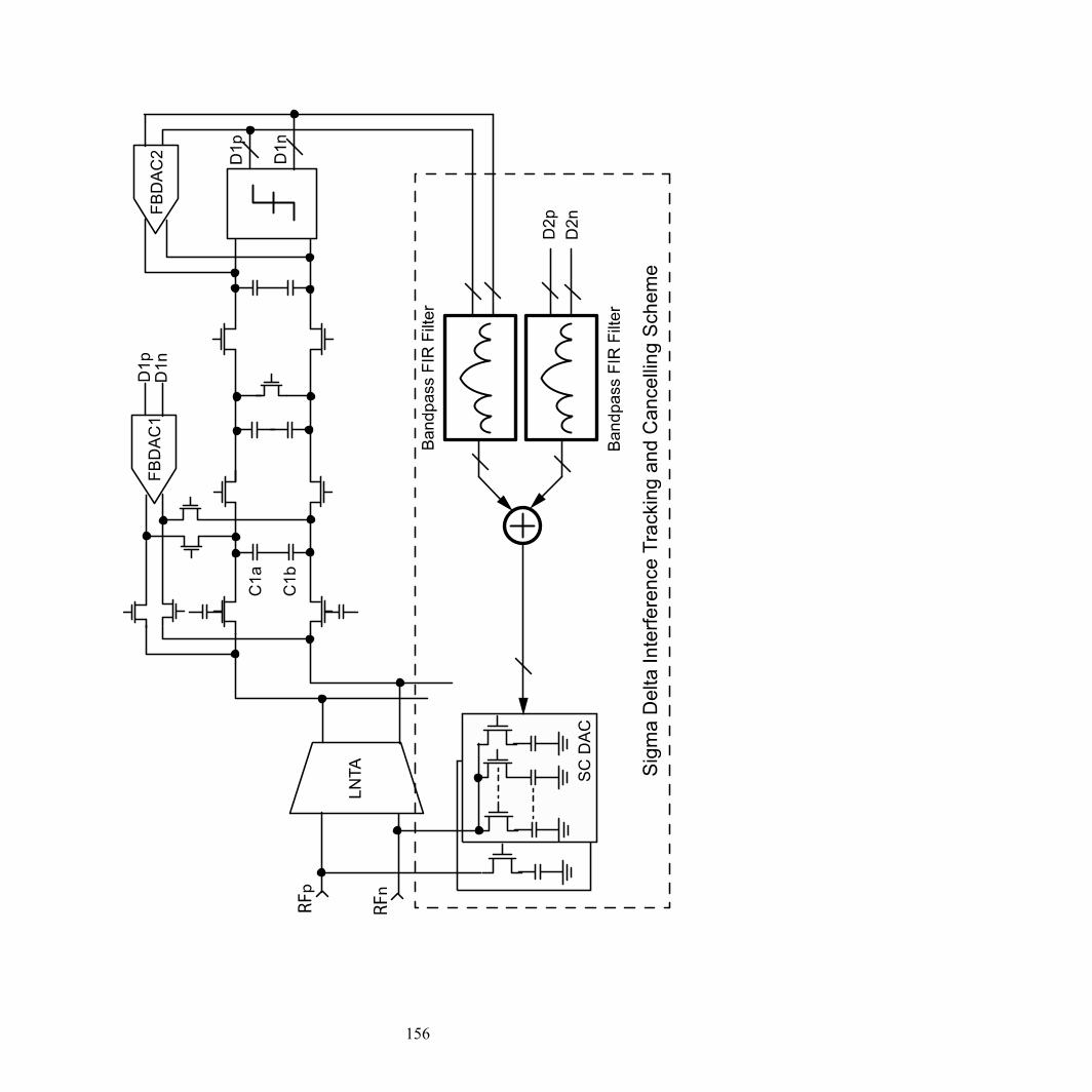
156
157
孤独に歩め…悪をなさず 求めるところは少なく…林の中の象のように
---『ダンマパダ』, 23章にある一節(330節)
158
Bibliography
[1] Apple Iphone 5c technical spec. Web.
[2] M. McHenry, D. McCloskey, D. Roberson, and J. MacDonald. Spectrum occupancy
Measurements. Chicago, Illinois, November 16-18, 2005. Web.
[3] J. Mitola, Software Radio: Survey, Critical Evaluation and Future Directions,
Proceedings of National Telesystems Conference. IEEE Press, May 1992.
[4] V. Giannini, P. Nuzzo, C. Soens, K. Vengattaramane, M. Steyaert, J. Ryckaert, M.
Gooul, B. Debaillie, J. Van Driessche, J. Cranickx, and M. Ingles. A 2mm2 0.1-to-
5GHz SDR Receiver in 45nm Digital CMOS. In International Solid-State Circuits
Conference, pages 408–409, 2009.
[5] R. Bagheri, A. Mirzaei, A. Chehrazi, M. Heidari, M. Lee, M. Mikhemar, W. Tang,
and A. Abidi. An 800-MHz-6-GHz Software-Defined Wireless Receiver in 90-nm
CMOS. IEEE Journal of Solid State Circuits, 41(12):2860–2876, December 2006.
[6] E. Org, R. Cyr, G. Dawe, and J. Kilpatrick. Software Defined Radio Architectures
for Mobile Commercial Applications. [online].
[7] K. Muhammad, D. Leipold, B. Staszewski, Y.-C. Ho, C. Hung, K. Maggio, C.
Fernando, T. Jung, J. Wallberg, J.-S. Koh, S. John, I. Deng, O. Moreira, R.
Staszewski, R. Katz and O. Friedman. A Discrete-Time Bluetooth Receiver in a
0.13um Digital CMOS Process. In Solid-State Circuits Conference, 2004. Digest of
Technical Papers. ISSCC. 2004 IEEE International, pages 268 Vol. 1, Feb. 2004
[8] K. Muhammad, Y.-C. Ho, J. Mayhugh, T.L., C.-M. Hung, T. Jung, I. Elahi, C. Lin, I.
Deng, C. Fernando, J. Wallberg, S. Vemulapalli, S. Larson, T. Murphy, D. Leipold,
P. Cruise, J. Jaenig, M,-C Lee, Staszewski, R.B., R. Staszewski and K. Maggio. The
first fully integrated quad-band GSM/GPRS receiver in a 90-nm digital CMOS
Process. IEEE Journal of Solid State Circuits, 41:1772-1783, August 2006.
[9] H. Lakdawala, J. Zhan, A. Ravi, S. Anderson, B. Carlton, R. Nicholls, N. Yaghini,
R. Bishop, S. Taylor, and K. Soumyanath. Multi-Band (1-6GHz), Sampled,
Sliding- IF Receiver with Discrete-Time Filtering in 90nm Digital CMOS Process.
In VLSI Circuits, 2006. Digest of Technical Papers. 2006 Symposium on, pages
230–231, 0-0 2006.
[10] J. Yuan. A charge sampling mixer with embedded filter function for wireless
applications. In Proc. 2nd, Int. Conf. Microwave and Millimeter Wave Technology,
pages 315–318, Beijing, China, 2000
159
[11] S. Karvonen, T. Riley, and J. Kostamovaara. A cmos quadrature charge-domain
sampling circuit with 66-db sfdr up to 100 mhz. Circuits and Systems I: Regular
Papers, IEEE Transactions on, 52(2):292–304, Feb. 2005.
[12] S. Karvonen, T. Riley, and J. Kostamovaara. Charge-domain fir sampler with pro-
grammable filtering coefficients. Circuits and Systems II: Express Briefs, IEEE
Transactions on, 53(3):192–196, March 2006.
[13] S. Karvonen, T. Riley, and J. Kostamovaara. A Low Noise Quadrature
Subsampling Mixer. In Circuits and Systems, 2001. ISCAS 2001. The 2001 IEEE
International Symposium on, volume 4, pages 790–793 vol. 4, May 2001.
[14] S. Lindfors, A. Parssinen, and K. Halonen. A 3-V 230-MHz CMOS decimation
sub-sampler. IEEE Transactions on Circuits and Systems - II, 50(3): 105–117,
March 2003.
[15] H. Pekau and J. Haslett. A 2.4 GHz cmos Sub-Sampling Mixer with Integrated
Filtering. Solid-State Circuits, IEEE Journal of, 40(11): 2159–2166, Nov. 2005.
[16] R. Schreier. ADCs and DACs: Marching Towards the Antenna. GIRAFE Forum in
International Solid State Circuits Conference, February 2003.
[17] R. Winoto and B. Nikolic ,A highly reconfigurable 400–1700MHz receiver using a
down-converting sigma-delta A/D with 59-dB SNR and 57-dB SFDR over 4-MHz
bandwidth, VLSI Circuits, 2009 Symposium, Page(s): 142 – 143
[18] L. Breems, E. van der Zwan, and J. Huijsing. A 1.8-mW CMOS sigma-delta
modulator with integrated mixer for A/D conversion of IF signals. Solid-State
Circuits, IEEE Journal of, 35(4): 468–475, Apr 2000
[19] F. Chen and B. Leung. A 0.25-mW Low-Pass Passive Sigma-Delta Modulator with
Built-in Mixer for a 10-MHz IF Input. Solid-State Circuits, IEEE Journal of,
32(6):774–782, Jun 1997.
[20] A. Namdar and B. Leung. A 400-MHz, 12-bit, 18-mW, IF Digitizer with Mixer
Inside a Sigma-Delta Modulator Loop. Solid-State Circuits, IEEE Journal of,
34(12):1765– 1776, Dec 1999.
[21] H. Tao and J. Khoury. A 400-Ms/s Frequency Translating Bandpass Sigma-Delta
Modulator. Solid-State Circuits, IEEE Journal of, 34(12):1741–1752, Dec 1999
[22] S. R. Norsworthy, R. Schreier, and G. C. Temes. Delta-Sigma data converters:
Theory, design, and simulation. IEEE Press, 1997.
[23] M. Ortmanns and F. Gerfers. Continuous-time sigma-delta A/D conversion:
Fundamentals, performance limits and robust implementations. Springer, 2006.
[24] A. Molnar, B. Lu, S. Lanzisera, B. Cook, and K. Pister, “An ultralow power 900

160
MHz RF transceiver for wireless sesor networks,” in Proc. IEEE Custom Integr.
Circuits Conf., Oct. 2004, pp 401-404.
[25] C. Andrews and A. Molnar “A Passive Mixer-First Receiver with Digitally
Controlled and Widely Tunable RF Interface”, IEEE Journal of Solid-State Circuits,
vol. 45, no. 12, December 2010.
[26] C. Andrews and A. Molnar “Implication of Passive Mixer Transparency for
Impedance Matching and Noise figure in Passive Mixer-first Receivers”, IEEE
Trans on Circuits and System-I, vol. 57, no. 12, December 2010.
[27] A. A. Abidi,“Software-defined radio receiver: Dream to reality”, IEEE
Communications Magazine, pp. 111-118, 2006.
[28] F. Rivet, Y. Deval, J-B. Begueret, D. Dallet, P. Cathelin, D. Belot, “The
experimental demonstration of a SASP-based full Software Radio Receiver”, IEEE
J. Solid-State Circuits, vol. 45, no. 6, pp. 979-988, Jun. 2010
[29] F. Chen and B. Leung, “A 0.25-mW low-pass passive sigma-delta modulator with
built-in mixer for a 10-MHz IF input”, IEEE J. Solid-State Circuits, vol. 32, no. 6,
pp. 774-782, Jun. 1997.
[30] R. Winoto and B. Nikolic, “A highly reconfigurable 4001700MHz receiver using a
down-converting sigma-delta A/D with 59-dB SNR and 57-dB SFDR over 4-MHz
bandwidth”, IEEE Symposium on VLSI Circuits, pp. 142-143, Jun. 2009.
[31] K. Koli, J. Jussila, P. Sivonen, S. Kallioninen and A. Parssinen, “A 900 MHz Direct
Receiver in 65nm CMOS”, in IEEE ISSCC Dig. Tech. Papers, Feb 2010, pp 64-65.
[32] A. K. Ong and B. A. Wooley, “A Two-path Bandpass ΔΣ Modulator for Digital IF
Extraction at 20 MHz”, IEEE J. Solid-State Circuits, vol. 32, no. 12, pp. 1920-1934,
Aug. 1997.
[33] R. Schreier and G. C. Temes, Understanding Delta-Sigma Data Converters. New
York: IEEE 2005.
[34] J. Gealow, M. Ashburn, C. H. Lou, S. Ho, P. Riehl, A. Shabra, J. Silva and Q. Yu,
“A 2.8 mW ΔΣ ADC with 83 dB DR and 1.92 MHz BW Using FIR Outer Feedback
and TIA-Biased Integrator”, IEEE Symposium on VLSI Circuits, pp. 42-43, Jun.
2011.
[35] Y. S. Shu, J. Y. Tsai, P. Chen, T. Y. Lo and P. C. Chiu, “A 28 fJ/conv CT ΔΣ
Modulator with 78 dB DR and 18 MHz BW in 28 nm CMOS Using a Highly
Digital Multibit Quantizer”, in IEEE ISSCC Dig. Tech. Papers, Feb, 2013, pp 268-
269.
[36] P. Shettigar and S. Pavan, “A 15 mW 3.6 GS/s CT ΔΣ ADC with 36 MHz
Bandwidth and 83 dB DR in 90 nm CMOS”, in IEEE ISSCC Dig. Tech. Papers,
161
Feb, 2012, pp 156-157.
[37] P. Shettigar and S. Pavan, “Design Techniques for Wideband Single-Bit
Continuous-Time ΔΣ Modulators with FIR Feedback DACs”, IEEE J. Solid-State
Circuits, vol. 47, no. 12, pp. 2865-2879, Dec 2012.
[38] J. A. Cherry and W. M. Snelgrove, “Clock Jitter and Quantizer Metability in
Continous-Time Delta-Sigma Modulators”, IEEE Tran. Circuits Syst. II, Analog
digit. Signal Process., vol. 46, no. 6 pp. 661-676, Jun 1999.
[39] PG. R. Silva, L. J. Breems, KA. A. Makinwa, R. Roovers and J. H. Huijsing, “An
IF-to-Baseband ΔΣ Modulator for AM/FM/IBOC Radio Receiver with 118 dB
Dynamic Range”, IEEE J. Solid-State Circuits, vol. 42, no. 5 pp. 1076-1089, Dec
2007.
[40] N. Beilleau, H. Aboushady, F. Montaudon and A. Cathelin, “A 1.3V 26mW 3.2GS/s
undersampled LC bandpass ADC for a SDR ISM-band receiver in 130nm CMOS”,
IEEE RFIC Symposium, pp. 383-386, Jun. 2009.
[41] B. Ovidiu and J. H. Huijsing, “Systematic design of Sigma-Delta analog-to-digital
converters”, Boston: Kluwer Academic Publishers, 2004.
[42] H. Tao, L. Toth and J. M. Khoury, “Analysis of timing jitter in bandpass sigma-
delta modulators”, IEEE Tran. Circuits Syst. II, Analog digit. Signal Process. vol.
46, no. 8 pp. 991-1001, Aug 1999.
[43] J. Yuan, “A charge sampling mixer with embedded filter function for wireless
applications”, in Proc. 2nd, Int. Conf. Microwave and Millimeter Wave Technology,
pages 315318, Beijing, China, 2000.
[44] R. Winoto, Downconverting Sigma-Delta A/D Converter for a Reconfigurable RF
Receiver, Technical Report, EECS Department, University of California, Berkeley.
2009
[45] I. Aoki, S.D. Kee, D.B. Rutledge, A. Hajimiri, “Distributed active transformer-a
new power-combining and impedance-transformation technique”, IEEE Tran.
Microwave Theory and Techniques, vol. 50, no. 1 pp. 316-331, 2002.
[46] L. Breems and J.H. Huijsing, “Cotinous-Time Sigma-Delta Modulation for A/D
Conversion in Radio Receivers”, Kluwer Academic, Boston, MA, 2002.
[47] M. Bolatkale, L.J. Breems, R. Rutten, K.A.A. Makinwa, “A 4-GHz Continuous-
Time D! ADC with 70-dB DR and -74 dBFS THD in 125-MHz BW, IEEE Journal
of Solid State Vol. 46, Issue. 12, Dec, 2011.
[48] A. Abidi, “Phase Noise and Jitter in CMOS Ring Oscillator, IEEE Journal of Solid
State Vol. 41, Issue. 8, Aug, 2006.

162
[49] A. Mirzaei and H. Darabi, “Analysis of Imperfections on Performance of 4-Phase
Passive-Mixer-Based High-Q Bandpass Filters in SAW-Less Receivers”, IEEE Tran.
Circuits Syst. I, Analog digit. Signal Process., vol. 58, no. 5 pp. 879-892, May 2011.
[50] S. Gupta, D. Gangopadhyay, H. Lakdawala, J.C. Rudell and D.J. Allstot, “A QPLL-
timed direct-RF sampling band-pass ADC with a 1.2 GHz tuning range in 0.13 m
CMOS,” Proc. IEEE Radio Frequency Integrated Circuits Symp., pp.25 -28 2008
[51] K. Koli, J. Jussila, P. Sivonen, S. Kallioinen, and A. Parssinen “A 900MHz direct
receiver in 65nm CMOS, ” in IEEE ISSCC Dig. Tech. Papers, Feb 2010, pp 64-65.
[52] B.K. Thandri and J. Silva-Martinez, “A 63 dB SNR, 75-mW Bandpass RF ΔΣ ADC
at 950 MHz Using 3.8-GHz Clock in 0.25-m SiGe BiCMOS Technology” IEEE J.
Solid-State Circuits, vol. 42, no. 2, pp. 269-279, Feb. 2007.
[53] J. Ryckaert, J. Borremans, B. Verbruggen, L. Bos, C. Armiento, J. Craninckx and G.
Van der Plas, “A 2.4 GHz Low-Power Sixth-Order RF Bandpass ΔΣ Converter in
CMOS” IEEE J. Solid-State Circuits, vol. 44, no. 11, pp. 2873-2880, Nov. 2009.
[54] J. Borremans, G. Mandal, V. Giannini, T. Sano, M. Ingels, B. Verbruggen and J.
Craninckx, “A 40nm CMOS highly linear 0.4-to-6GHz receiver resilient to 0dBm
out-of-band blockers” in IEEE ISSCC Dig. Tech. Papers, Feb 2011, pp 62-64.
[55] H. Shibata, R. Schreier, W. Yang, A. Shaikh, D. Paterson, T.C. Caldwell, D. Alldred
and P. Lai “A DC-to-1 GHz Tunable RF ΔΣ ADC Achieving DR = 74 dB and BW =
150 MHz at f0 = 450 MHz Using 550 mW,” IEEE J. Solid-State Circuits, vol. 47,
no. 12, pp 2888-2897, Dec 2012.
[56] M. Englund, K.B. Ostman, O. Viitala, M. Kaltiokallio, Kari. Stadius, K. Koli and J.
Ryynanen “A programmable 0.7-to-2.7 GHz Direct ΔΣ receiver in 40 nm CMOS,”
IEEE ISSCC Digest, pp 470-471, Feb 2014.
[57] Geffroy, V.; De Astis, G.; Bergeault, E “RF mixers using standard digital CMOS
0.35 μm process” Microwave Symposium Digest, vol. 1, 2001,pp. 83–86.
[58] D. Tayloe. “A Low-noise, High-performance Zero IF Quadrature Detector/
Preamplifier” RF Design, Mar. 2003,
[59] A. Mirzaei, H. Darabi, J. Leete, X. Chen, K. Juan, and A. Yazdi, “Analysis and
optimization of current-driven passive mixers in narrowband direct conversion
receivers,” IEEE J.Solid-State Circuits, pp. 2678–2688, Oct. 2009.
[60] N. Kim, L. Larson, and V. Aparin, “A highly linear SAW-less CMOS receiver using
a mixer with embedded Tx filtering for CDMA,” IEEE J.Solid-State Circuits, pp.
2126–2137, Aug. 2009.
[61] M. Soer, E. Klumperink, Z. Ru, F.E. van Vliet, and B. Nauta, “A 0.2-to-2.0GHz
65nm CMOS receiver without LNA achieving 11dbm IIP3 and 6.5 dB NF,” IEEE

163
ISSCC Dig. Tech. Papers, vol. 52, Feb. 2009, pp. 222-223.
[62] C. Andrews and A.C. Molnar, “A Passive Mixer-First Receiver with Digitally
Controlled and Widely Tunable RF Interface,” IEEE J. Solid-State Circuits, vol. 45,
2010.
[63] C. Andrews and A.C. Molnar, “Implications of Passive Mixer Transparency for
Impedance Matching and Noise Figure in Passive Mixer-First Receivers,”
Transactions on Circuits and Systems I: Regular Papers,, vol.57, 2010.
[64] H. Khatri, L. Liu, T. Chang, P. Gudem, and L. Larson, “A SAW-less CDMA
receiver front-end with single-ended LNA and single-balanced mixer with 25%
duty-cycle LO in 65nm CMOS,” IEEE Radio FrequencyIntegrated Circuits Symp.,
pp. 13–16, Jun. 2009.
[65] Soer, M.C.M.; Klumperink, E.A.M.; de Boer, P.-T.; van Vliet, F.E.; Nauta,
B.,”Unified Frequency-Domain Analysis of Switched-Series- RC Passive Mixers
and Samplers ” Circuits and Systems I: Regular Papers, IEEE Transactions on, Vol.
57, pp. 2618-2631, 2010
[66] J. Borremans, et al. “A 40nm CMOS highly linear 0.4-to-6GHz receiver resilient to
0dBm out-of-band blockers,” ISSCC 2011.
[67] I.S. –C.Lu, et al. “A SAW-less GSM/GPRS/EDGE receiver embedded in a 65nm
CMOS SOC,” ISSCC 2011
[68] D. Murphy, A.A Hafez, A. Mirzaei, M. Mikhemar, H. Darabi, M.F. Chang and A.A.
Abidi “A Blocker-Tolerant Wideband Noise-Cancelling Receiver with a 2dB Noise
Figure,” ISSCC 2012.
[69] C. Liu and M Damgaard, “IP2 & IP3 Nonlinearity Spec for 3G/WCDMA
Receivers,” High Frequency Electronics, June 2009.
[70] X. Peng and W. Sansen, “AC Boos8ng Compensa8on Scheme for Low-Power
Mul8stage Amplifiers,” JSCC Vol 39, NO. 11, Nov, 2004
[71] L. Sundstrom, et al., “A Receiver for LTE Rel-11 and Beyond Suppor8ng Non-
Con8guous Carrier Aggrega8on,” ISSCC 2013
[72] E. Alpman, et al., “Two-Channel Receiver Back-End Using Sta8cally Calibrated
HRM with > 70dB 3rd and the harmonic Rejec8on for Carrier Aggrega8on in 32nm
CMOS,” VLSI 2013
[73] P.G. Gray, P.J. Hurst, S.H. Lewis and R.G. Meyer “Analysis and Design of Analog
Integrated Circuit” Wiley; 5th
Edition, Jan, 2009.
[74] M. Mikhemar, A. Mirzaei, A. Hadji-Abdolhamid, J. Chiu and H. Darabi “A 13.5mA
sub-2.5dB NF multi-band receiver,” VLSI Circuit Symposium 2012. Page(s): 82-83
164
[75] A. Niknejad, EE242 Advanced Analog/RF Circuit Design Lecture slides, UC
Berkeley, 2007
[76] Z. Ru, E.A.M. Klumperink, C.E. Saavedra, B. Nauta, “A 300–800 MH Tunable
Filter and Linearized LNA Applied in a Low-Noise Harmonic-Rejection RF-
Sampling Receiver,” Solid-State Circuits, IEEE Journal of Volume: 45 , Issue: 5
Publication Year: 2010, Page(s): 967- 978.
[77] B. Marholev, M. Pan, E. Chien, L. Zhang, R. Roufoogaran, S. Wu, I. Bhatti, T.- H.
Lin, M. Kappes, S. Khorram, S. Anand, A. Zolfaghari, J. Castaneda, C. Chien, B.
Ibrahim, H. Jensen, H. Kim, P. Lettieri, S. Mak, J. Lin, Y. Wong, R. Lee, M. Syed,
M. Rofougaran, and A. Rofougaran. A Single-Chip Bluetooth EDR Device in
0.13μm CMOS. In Solid-State Circuits Conference, 2007. ISSCC 2007. Digest of
Technical Papers. IEEE International, pages 558–759, Feb. 2007.
[78] L. Nathawad, D. Weber, S. Abdollahi, P. Chen, S. Enam, B. Kaczynski, A.
Kheirkhahi, M. Lee, S. Limotyrakis, K. Onodera, K. Vleugels, M. Zargari, and B.
Wooley. An IEEE 802.11a/b/g SoC for Embedded WLAN Applications. In Solid-
State Circuits Conference, 2006. ISSCC 2006. Digest of Technical Papers. IEEE
In- ternational, pages 1430–1439, Feb. 2006.
[79] Y. Palaskas, A. Ravi, S. Pellerano, B. Carlton, M. Elmala, R. Bishop, G. Banerjee,
R. Nicholls, S. Ling, S. Taylor, and K. Soumyanath. A 5GHz 108Mb/s 2x2 MIMO
Transceiver with Fully Integrated +16dBm PAs in 90nm CMOS. In Solid-State Cir-
cuits Conference, 2006. ISSCC 2006. Digest of Technical Papers. IEEE
International, pages 1420–1429, Feb. 2006.
[80] A. Behzad, K. Carter, E. Chien, S. Wu, M. Pan, C. Lee, T. Li, J. Leete, S. Au, M.
Kappes, Z. Zhou, D. Ojo, L. Zhang, A. Zolfaghari, J. Castanada, H. Darabi, B.
Yeung, R. Rofougaran, M. Rofougaran, J. Trachewsky, T. Moorti, R. Gaikwad, A.
Bagchi, J. Rael, and B. Marhoiev. A Fully Integrated MIMO Multi-Band Direct-
Conversion CMOS Transceiver for WLAN Applications (802.11n). In Solid-State
Cir- cuits Conference, 2007. ISSCC 2007. Digest of Technical Papers. IEEE
International, pages 560–622, Feb. 2007.
[81] O. Degani, M. Ruberto, E. Cohen, Y. Eilat, B. Jann, F. Cossoy, N. Telzhensky, T.
Maimon, G. Normatov, R. Banin, O. Ashkenazi, A. Ben Bassat, S. Zaguri, G. Hara,
M. Zajac, E. Shaviv, S. Wail, A. Fridman, R. Lin, and S. Gross. A 1x2 MIMO
Multi-Band CMOS Transceiver with an Integrated Front-End in 90nm CMOS for
802.11a/g/n WLAN Applications. In Solid-State Circuits Conference, 2008. ISSCC
2008. Digest of Technical Papers. IEEE International, pages 356–619, Feb. 2008.
[82] S. Tadjpour, E. Cijvat, E. Hegazi, and A. Abidi. A 900-MHz Dual-Conversion
Low-IF GSM Receiver in 0.35μm CMOS. Solid-State Circuits, IEEE Journal of,
36(12):1992– 2002, Dec 2001.
[83] O. Erdogan, R. Gupta, D. Yee, J. Rudell, J.-S. Ko, R. Brockenbrough, S.-O. Lee, E.
Lei, J. L. Tham, H. Wu, C. Conroy, and B. Kim. A Single-Chip Quad-Band
165
GSM/GPRS Transceiver in 0.18 μm Standard CMOS. In Solid-State Circuits Con-
ference, 2005. Digest of Technical Papers. ISSCC. 2005 IEEE International, pages
318–601 Vol. 1, Feb. 2005.
[84] Y. Le Guillou, O. Gaborieau, P. Gamand, M. Isberg, P. Jakobsson, L. Jonsson, D.
Le Deaut, H. Marie, S. Mattisson, L. Monge, T. Olsson, S. Prouet, and T. Tired.
Highly Integrated Direct Conversion Receiver for GSM/GPRS/EDGE with On-
Chip 84-dB Dynamic Range Continuous-Time ADC. Solid-State Circuits, IEEE
Jour- nal of, 40(2):403–411, Feb. 2005.
[85] H. Darabi, A. Zolfaghari, H. Jensen, J. Leete, B. Mohammadi, J. Chiu, T. Li, Z.
Zhou, P. Lettieri, Y. Chang, A. Hadji, P. Chang, M. Nariman, I. Bhatti, A. Medi, L.
Serrano, J. Welz, K. Shoarinejad, S. Hasan, J. Castaneda, J. Kim, H. Tran, P.
Kilcoyne, R. Chen, B. Lee, B. Zhao, B. Ibrahim, M. Rofougaran, and A.
Rofougaran. A Fully Integrated Quad-Band GPRS/EDGE Radio in 0.13μm CMOS.
In Solid-State Circuits Conference, 2008. ISSCC 2008. Digest of Technical Papers.
IEEE International, pages 206–607, Feb. 2008.
[86] V. Aparin, N. Kim, G. Brown, Y. Wu, A. Cicalini, S. Kwok, and C. Persico. A
Fully- Integrated Highly Linear Zero-IF CMOS Cellular CDMA Receiver. In Solid-
State Circuits Conference, 2005. Digest of Technical Papers. ISSCC. 2005 IEEE
Interna- tional, pages 324–601 Vol. 1, Feb. 2005.
[87] D. Kaczman, M. Shah, N. Godambe, M. Alam, H. Guimaraes, L. Han, M.
Rachedine, D. Cashen, W. Getka, C. Dozier, W. Shepherd, and K. Couglar. A
Single-Chip Tri- Band (2100, 1900, 850/800 MHz) WCDMA/HSDPA Cellular
Transceiver. Solid-State Circuits, IEEE Journal of, 41(5):1122–1132, May 2006.
[88] B. Tenbroek, J. Strange, D. Nalbantis, C. Jones, P. Fowers, S. Brett, C. Beghein,
and F. Be↵a. Single-Chip Tri-Band WCDMA/HSDPA Transceiver without
External SAW Filters and with Integrated TX Power Control. In Solid-State
Circuits Conference, 2008. ISSCC 2008. Digest of Technical Papers. IEEE
International, pages 202–607, Feb. 2008.
[89] J. Zipper, R. Vazny, L. Maurer, M. Wilhelm, T. Greifeneder, and A. Holm. A single-
Chip Dual-Band CDMA2000 Transceiver in 0.13μm CMOS. In Solid-State Circuits
Conference, 2007. ISSCC 2007. Digest of Technical Papers. IEEE International,
pages 342–607, Feb. 2007.
[90] Z. Li, W. Ni, J. Ma, M. Li, D. Ma, D. Zhao, J. Mehta, D. Hartman, X. Wang, K. O,
and K. Che. A Dual-Band CMOS Transceiver for 3G TD-SCDMA. In Solid-State
Circuits Conference, 2007. ISSCC 2007. Digest of Technical Papers. IEEE
International, pages 344–607, Feb. 2007.
[91] D. Sahu, A. Das, Y. Darwhekar, S. Ganesan, G. Rajendran, R. Kumar, B. Chan-
drashekar, A. Ghosh, A. Gaurav, T. Krishnaswamy, A. Goyal, S.
Bhagavatheeswaran, K. M. Low, N. Yanduru, S. Dhamankar, and S. Venkatraman.
166
A 90nm CMOS Single- Chip GPS Receiver with 5dBm out-of-band IIP3 2.0dB
NF. In Solid-State Circuits Conference, 2005. Digest of Technical Papers. ISSCC.
2005 IEEE International, pages 308–600 Vol. 1, Feb. 2005.
[92] V. Delia Torre, M. Conta, R. Chokkalingam, G. Cusmai, P. Rossi, and R. Svelto. A
20mW 3.24mm2 Fully Integrated GPS Radio for Cell-Phones. In Solid-State
Circuits Conference, 2006. ISSCC 2006. Digest of Technical Papers. IEEE
International, pages 1902–1911, Feb. 2006.
[93] Broadcom Corp. BRCM2075 Product Brief.
[94] Broadcom Corp. BRCM4329 Product Brief.
[95] L. Lin, N. Wongkomet, Y. D., C. Lin, M. He, B. Nissim, S. Lyuee, P. Yu, T. Sepke,
S. Shekarchian, L. Tee, P. Muller, J. Tam, and T. Cho. A Fully Integrated 2x2
MIMO Dual-Band Dual-Mode Direct-Conversion CMOS Transceiver for
WiMAX/WLAN Applications. In International Solid-State Circuits, 2009.
[96] D. Kaczman, M. Shah, M. Alam, M. Rachedine, D. Cashen, L. Han, and A. Ragha-
van. A SingleChip 10-Band WCDMA/HSDPA 4-Band GSM/EDGE SAW-less
CMOS Receiver with DigRF 3G Interface and +90 dBm IIP2. Solid-State Circuits,
IEEE Journal of, 44(3):718–739, March 2009.
[97] B. Bakkaloglu, P. Fontaine, A. Mohieldin, S. Peng, S. J. Fang, and F. Dulger. A
1.5- V multi-mode quad-band RF receiver for GSM/EDGE/CDMA2K in 90-nm
digital CMOS process. Solid-State Circuits, IEEE Journal of, 41(5):1149–1159,
May 2006.
[98] T. Sowlati, J. Agarwal, J. Cho, T. Obkircher, and M. El Said. Single-Chip Multi-
band WCDMA/HSDPA/HSUPA/EGPRS Tranceiver with Diversity Receiver and
3G DigRF Interface without SAW Filters in Transmitter/3G Receiver Paths. In
Interna- tional Solid State Circuits Conference, pages 116–117, 2009.
[99] A. Hadjichristos, A. Cassia, H. Kim, and C. Park. Single-Chip RF CMOS
UMTS/EGSM Transceiver with Integrated Receive Diversity and GPS. In Inter-
national Solid-State Circuits Conference, pages 118–119, 2009.
[100] V. Giannini, P. Nuzzo, C. Soens, K. Vengattaramane, M. Steyaert, J. Ryckaert, M.
Goffioul, B. Debaillie, J. Van Driessche, J. Craninckx and M. Ingels, "A 2mm2 0.1-
to-5GHz SDR receiver in 45nm digital CMOS," In International Solid-State
Circuits Conference, pages 409–410, 2009.
[101] Q. Huang, J. Rogin, X. Chen, D. Tschopp, T. Burger, T. Christen, D.
Papadopoulos, I. Kouchev, C. Martelli, T. Dellsperger, "A tri-band SAW-less
WCDMA/HSPA RF CMOS transceiver with on-chip DC-DC converter
connectable to battery," In International Solid-State Circuits Conference, pages 60–
61, 2010.
167
[102] T. Dellsperger, D. Tschopp, J. Rogin, Y. Chen, T. Burger and Q. Huang"A quad-
band class-39 RF CMOS receiver for evolved EDGE," In International Solid-State
Circuits Conference, pages 56–57, 2010.
[103] H. Moon, L. Sangyoub, S. Heo, H. Yu, J. Yu, J. Chang, S. Choi, B. Park "A 23mW
fully integrated GPS receiver with robust interferer rejection in 65nm CMOS," In
International Solid-State Circuits Conference, pages 68–69, 2010.
[104] C. Lee, A. Behzad, B. Marholev, V. Magoon, I. Bhatti; Li, D. ; Bothra, S. ; Afsahi,
A. ; Ojo, D. ; Roufoogaran, R. ; Li, T. ; Yuyu Chang ; Rao, K.R. ; Au, S. ;
Seetharam, P. ; Carter, K. ; Rael, J. ; MacIntosh, M. ; Lee, B. ; Rofougaran, M. ;
Rofougaran, R. ; Hadji-Abdolhamid, A. ; Nariman, M. ; Khorram, S. ; Anand, S. ;
Chien, E. ; Wu, S. ; Barrett, C. ; Lijun Zhang ; Zolfaghari, A. ; Darabi, H. ;
Sarfaraz, A. ; Ibrahim, B. ; Gonikberg, M. ; Forbes, M. ; Fraser, C. ; Gutierrez, L. ;
Gonikberg, Y. ; Hafizi, M. ; Mak, S. ; Castaneda, J. ; Kim, K. ; Zhenhua Liu ;
Bouras, S. ; Chien, K. ; Chandrasekhar, V. ; Chang, P. ; Li, E. ; Zhimin Zhao "A
multistandard, multiband SoC with integrated BT, FM, WLAN radios and
integrated power amplifier, " In International Solid-State Circuits Conference,
pages 455–456, 2010.
[105] Deguchi, J. ; Miyashita, D. ; Ogasawara, Y. ; Takemura, G. ; Iwanaga, M. ; Sami,
K. ; Ito, R. ; Wadatsumi, J. ; Tsuda, Y. ; Oda, S. ; Kawaguchi, S. ; Itoh, N. ;
Hamada, M. "A fully integrated 2×1 dual-band direct-conversion transceiver with
dual-mode fractional divider and noise-shaping TIA for mobile WiMAX SoC in
65nm CMOS," In International Solid-State Circuits Conference, pages 456–457,
2010.
[106] Lu, I.S. ; Chi-Yao Yu ; Yen-Horng Chen ; Lan-Chou Cho ; Sun, C.E. ; Chih-Chun
Tang ; Chien, G. "A SAW-less GSM/GPRS/EDGE receiver embedded in a 65nm
CMOS SoC," In International Solid-State Circuits Conference, pages 356–357,
2011.
[107] Nilsson, M. ; Mattisson, S. ; Klemmer, N. ; Anderson, M. ; Arnborg, T. ; Caputa, P.
; Ek, S. ; Lin Fan ; Fredriksson, H. ; Garrigues, F. ; Geis, H. ; Hagberg, H. ;
Hedestig, J. ; Hu Huang ; Kagan, Y. ; Karlsson, N. ; Kinzel, H. ; Mattsson, T. ;
Mills, T. ; Fenghao Mu ; Mårtensson, A. ; Nicklasson, L. ; Oredsson, F. ; Ozdemir,
U. ; Park, F. ; Pettersson, T. ; P hlsson, T. ; P lsson, M. ; Ramon, S. ; Sandgren, M.
; Sandrup, P. ; Stenman, A. ; Strandberg, R. ; Sundstr m, L. ; Tillman, F. ; Tired, T.
; Uppathil, S. ; Walukas, J. ; Westesson, E. ; Xuhao Zhang ; Andreani, P. "A 9-band
WCDMA/EDGE transceiver supporting HSPA evolution," In International Solid-
State Circuits Conference, pages 354–355, 2011.
[108] Cicalini, A. ; Aniruddhan, Sankaran ; Apte, R. ; Bossu, F. ; Choksi, O. ; Filipovic,
D. ; Godbole, K. ; Tsai-Pi Hung ; Komninakis, C. ; Maldonado, D. ; Narathong, C. ;
Nejati, B. ; O'Shea, D. ; Xiaohong Quan ; Rangarajan, R. ; Sankaranarayanan, J. ;
See, A. ; Sridhara, R. ; Bo Sun ; Wenjun Su ; van Zalinge, K. ; Gang Zhang ;
Sahota, K. "A 65nm CMOS SoC with embedded HSDPA/EDGE transceiver,
168
digital baseband and multimedia processor," In International Solid-State Circuits
Conference, pages 366–367, 2011.
[109] X. He and H. Kundr "A compact SAW-less multiband WCDMA/GPS receiver
front-end with translational loop for input matching," In International Solid-State
Circuits Conference, pages 373–374, 2011.
[110] Beffa, F. ; Tze Yee Sin ; Tanzil, A. ; Ivory, D. ; Tenbroek, B. ; Strange, J. ; Ali-
Ahmad, W. "A receiver for WCDMA/EDGE mobile phones with inductorless
front-end in 65nm CMOS," In International Solid-State Circuits Conference, pages
370–371, 2011.
[111] Yuan-Hung Chung; Min Chen ; Wei-Kai Hong ; Jie-Wei Lai ; Sheng-Jau Wong ;
Chien-Wei Kuan ; Hong-Lin Chu ; Chihun Lee ; Chih-Fan Liao ; Hsuan-Yu Liu ;
Hong-Kai Hsu ; Li-Chun Ko ; Kuo-Hao Chen ; Chao-Hsin Lu ; Tsung-Ming Chen ;
YuLi Hsueh ; Chunwei Chang ; Yi-Hsien Cho ; Chih-Hsien Shen ; Yuan Sun ; Eng-
Chuan Low ; Xudong Jiang ; Deyong Hu ; Weimin Shu ; Jhy-Rong Chen ; Jui-Lin
Hsu ; Chia-Jui Hsu ; Zhan, J.-H.C. ; Shana'A, O. ; Guang-Kaai Dehng ; Chien, G.
"A 4-in-1 (WiFi/BT/FM/GPS) connectivity SoC with enhanced co-existence
performance in 65nm CMOS," In International Solid-State Circuits Conference,
pages 172–174, 2012.
[112] Kumar, R.; Krishnaswamy, T. ; Rajendran, G. ; Sahu, D. ; Sivadas, A. ; Nandigam,
M. ; Ganeshan, S. ; Datla, S. ; Kudari, A. ; Bhasin, H. ; Agrawal, M. ; Narayan, S. ;
Dharwekar, Y. ; Garg, R. ; Edayath, V. ; Suseela, T. ; Jayaram, V. ; Ram, S. ;
Murugan, V. ; Kumar, A. ; Mukherjee, S. ; Dixit, N. ; Nussbaum, E. ; Dror, J. ;
Ginzburg, N. ; EvenChen, A. ; Maruani, A. ; Sankaran, S. ; Srinivasan, V. ;
Rentala, V. "A fully integrated 2×2 b/g and 1×2 a-band MIMO WLAN SoC in
45nm CMOS for multi-radio IC," In International Solid-State Circuits Conference,
pages 328–329, 2013.
[113] Chun Geik Tan; Fei Song ; Tieng Yi Choke ; Ming Kong ; De-Cheng Song ; Chee-
Hong Yong ; Weimin Shu ; Zong Hua You ; Yi-Hsien Lin ; Shanaa, O. "A
universal GNSS (GPS/Galileo/Glonass/Beidou) SoC with a 0.25mm2 radio in
40nm CMOS," In International Solid-State Circuits Conference, pages 334–335,
2013.
[114] H. Khatri, P.S. Gudem and L.E. Larson, “Distortion in Current Commutating
Passive CMOS Downconversion Mixers,” IEEE Transaction on MTT, Vol, 57, No.
11, Nov. 2009.
[115] Federal Communication Commission. “History of Communications,” Last modified
November,11, 2005. http://transition.fcc.gov/omd/history/
[116] Abdollahi-Alibeik, S. ; Weber, D. ; Dogan, H. ; Si, W.W. ;Baytekin, B. ; Komijani,
A. ; Chang, R. ; Vakili-Amini, B. ;MeeLan Lee ; Gan, H. ; Rajavi, Y. ; Samavati,
H. ;Kaczynski, B. ; Sang-Min Lee ; Limotyrakis, S. ;Hyunsik Park ; Chen,
P. ; Park, P. ; Chen, M.S. ; Chang, A.; Oh, Y. ; Yang, J.J. ; Lin, E.C. ; Nathawad,
169
L. ; Onodera, K.; Terrovitis, M. ; Mendis, S. ; Kai Shi ; Mehta, S. ;Zargari, M. ; Su,
D. “A 65nm dual-band 3-stream 802.11n MIMO WLAN SoC,” In International
Solid-State Circuits Conference, pages 170–172, 2011.
[117] Ming He ; Winoto, R. ; Xiang Gao ; Loeb, W. ; Signoff, D. ;Wai Lau ; Yuan
Lu ; Donghong Cui ; Kun-Seok Lee ;Sai-Wang Tam ; Godoy, P. ; Yung
Chen ; Sanghoon Joo ;Hu, C. ; Paramanandam, A.A. ; Xiaoyue Wang ;Chi-Hung
Lin ; Li Lin, “A 40nm Dual-Band 3-stream 802.11a/g/n/ac MIMO WLAN SoC
with 1.1Gb/s Over the Air Throughput,” In International Solid-State Circuits
Conference, pages 350–351, 2014.
[118] Ming-Da Tsai ; Chih-Fan Liao ; Chi-Yun Wang ; Yi-Bin Lee ;Tzeng, B. ; Guang-
Kaai Dehng, “A Multi-Band Inductor-Less SAW-Less 2G/3G-TD-SCDMA
Cellular Recevier in 40nm CMOS,” In International Solid-State Circuits
Conference, pages 354–355, 2014.
[119] T. Lee, The Design of CMOS Radio-Frequency Integrated Circuits. Cambridge,
U.K.: Cambridge Univ. Press, 2004.
[120] S. Zhou and M.-C. Chang, “A CMOS passive mixer with low flicker noise for low-
power direct-conversion receiver,” IEEE J. Solid-State Circuits, vol. 40, no. 5, pp.
1084–1093, May 2005.
[121] D. Manstretta and F. Svelto, “Analysis and optimization of IIP2 in CMOS direct
down-converters,” in Proc. IEEE Custom Integrated Circuits Conf., 2002, pp. 243–
246.
[122] M. Lehne, J. Stonick, and U. Moon, “An adaptive offset cancellation mixer for
direct conversion receivers in 2.4 GHz CMOS,” in Proc. IEEE Int. Circuits Syst.
Symp., 2000, vol. 1, pp. 319–322.
[123] W. Redman-White and D. M. W. Leenaerts, “1/f noise in passive CMOS mixers
for low and zero IF integrated receivers,” in Proc. IEEE Eur. Solid-State Circuits
Conf., Sep. 18–20, 2001, pp. 41–44
[124] W. Sansen, Analog Design Essentials. Dordrecht, The Netherlands: Springer, 2006.