Embed Size (px)
Citation preview
Next Generation MEMS ManufacturingThe ConFab 2017
Alissa M. Fitzgerald, Ph.D., Founder & Managing Member

Overview
• About AMFitzgerald
• Retrospective: MEMS technology history and markets
• Next generation MEMS processes and devices
• A dilemma for foundries and MEMS startups
The ConFab 2017, San Diego, CA © AMFitzgerald 2017Page 2
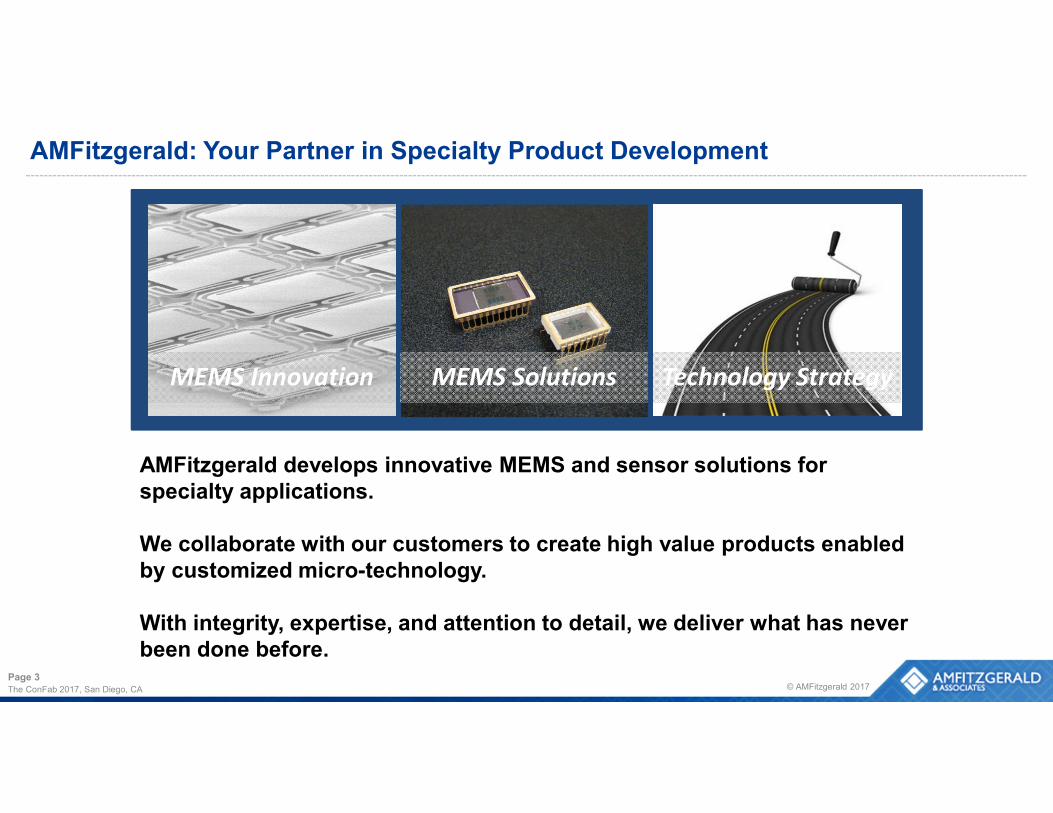
AMFitzgerald: Your Partner in Specialty Product Development
© AMFitzgerald 2017Page 3
MEMS Innovation MEMS Solutions Technology Strategy
The ConFab 2017, San Diego, CA
AMFitzgerald develops innovative MEMS and sensor solutions for specialty applications.
We collaborate with our customers to create high value products enabled by customized micro-technology.
With integrity, expertise, and attention to detail, we deliver what has never been done before.
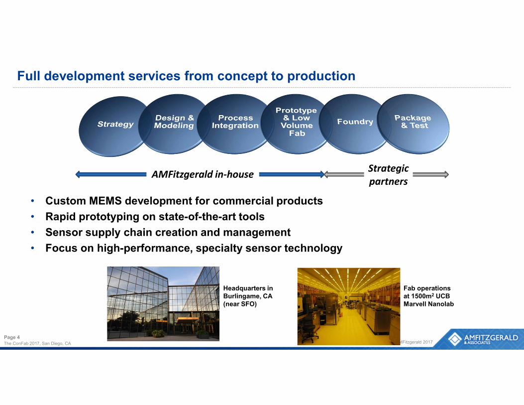
• Custom MEMS development for commercial products
• Rapid prototyping on state-of-the-art tools
• Sensor supply chain creation and management
• Focus on high-performance, specialty sensor technology
© AMFitzgerald 2017
AMFitzgerald in-houseStrategic partners
Full development services from concept to production
Page 4The ConFab 2017, San Diego, CA
Fab operations at 1500m2 UCB Marvell Nanolab
Headquarters in Burlingame, CA (near SFO)
© AMFitzgerald 2017Page 5
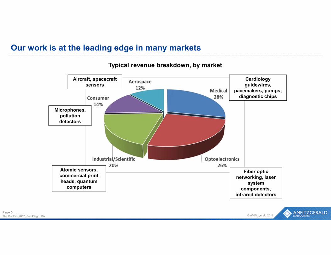
Our work is at the leading edge in many markets
The ConFab 2017, San Diego, CA
Typical revenue breakdown, by market
Cardiology guidewires,
pacemakers, pumps; diagnostic chips
Fiber optic networking, laser
system components,
infrared detectors
Atomic sensors, commercial print heads, quantum
computers
Microphones, pollution detectors
Aircraft, spacecraft sensors

MEMS Retrospective, 1980-2010
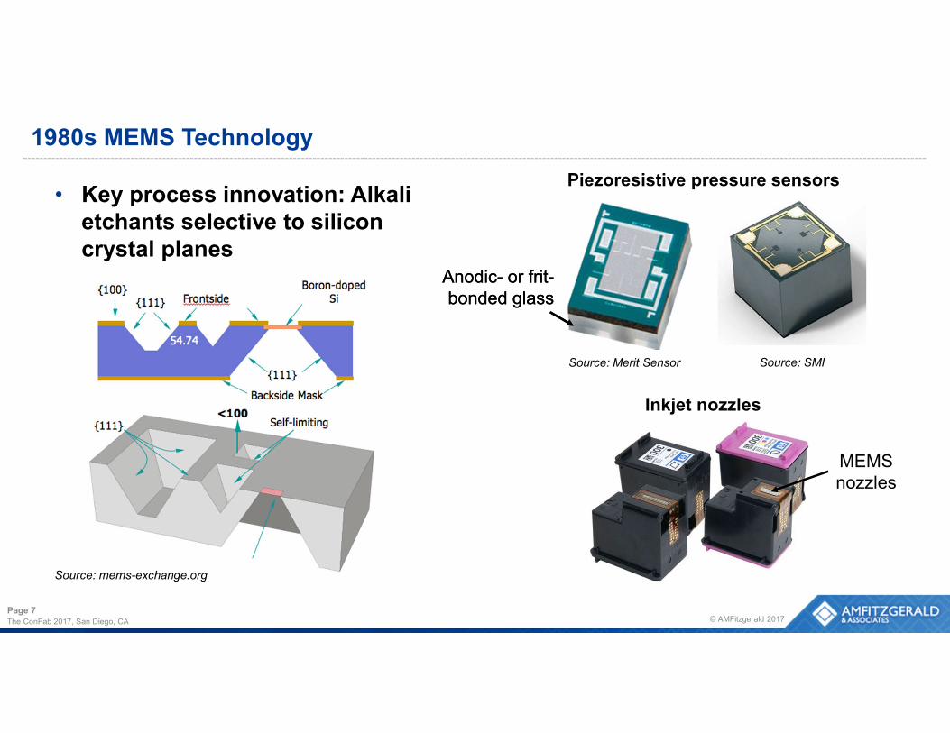
1980s MEMS Technology
• Key process innovation: Alkali etchants selective to silicon crystal planes
The ConFab 2017, San Diego, CA © AMFitzgerald 2017Page 7
Source: mems-exchange.org
Source: Merit Sensor Source: SMI
Anodic- or frit-bonded glass
Piezoresistive pressure sensors
Inkjet nozzles
Anodic- or frit-bonded glass
MEMS nozzles

1990s MEMS Technology
• Key process innovation: CMOS-like MEMS, using sacrificial etch of layers
The ConFab 2017, San Diego, CA © AMFitzgerald 2017Page 8
Sacrificial etch frees thin film mechanical structures
Analog Devices ADXL50
TI Digital Light Projection (DLP)
MEMS
BiCMOSreadout circuitry
Pixel array
Accelerometer

1990s-2000s MEMS Technology
• Key process innovation: Deep reactive ion etch (DRIE), or “the Bosch process”
• CMOS-friendly piezoelectric: AlN
The ConFab 2017, San Diego, CA © AMFitzgerald 2017Page 9
DRIE
ST C5L24AAMFitzgerald
Avago Film Bulk Acoustic Resonator (FBAR)
“Comb drive” shapes used in many MEMS accelerometers, gyroscopes, actuators
>20:1 aspect ratio

MEMS industry dynamics
The ConFab 2017, San Diego, CA © AMFitzgerald 2017Page 10
Annual sales,
USD M$
1000
500
200
100
“Major Players”
Dominate the twohigh volume
markets: consumer and automotive
“The Long Tail”
The other 400+ MEMS companies with emerging
technologies
Company ranking by annual sales
#1 #30
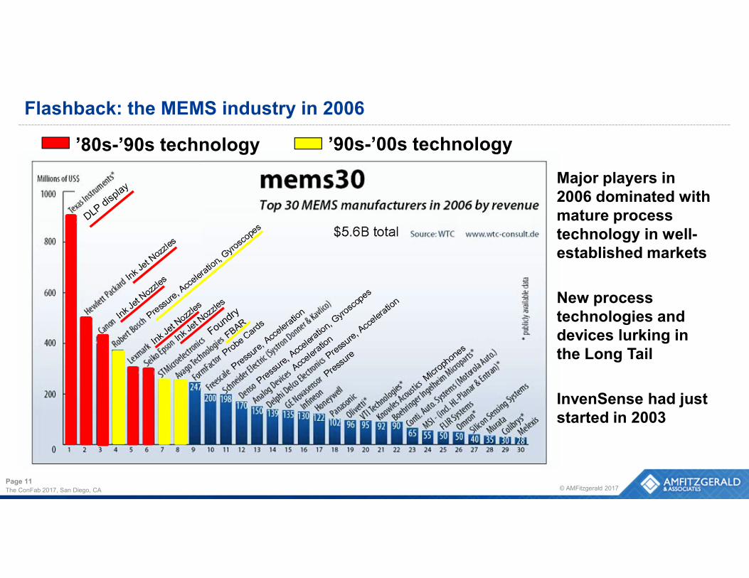
Flashback: the MEMS industry in 2006
The ConFab 2017, San Diego, CA © AMFitzgerald 2017Page 11
’80s-’90s technology ’90s-’00s technology
Major players in 2006 dominated with mature process technology in well-established markets
New processtechnologies and devices lurking in the Long Tail
InvenSense had just started in 2003
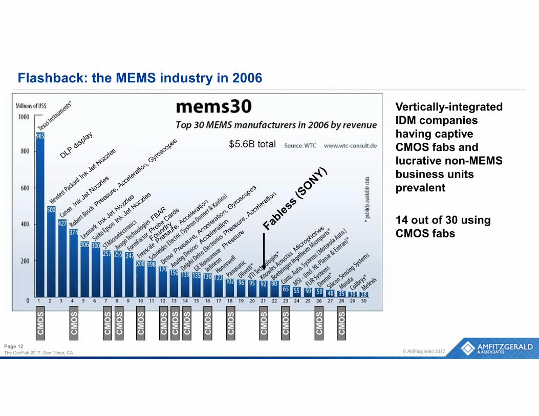
Flashback: the MEMS industry in 2006
The ConFab 2017, San Diego, CA © AMFitzgerald 2017Page 12
Vertically-integrated IDM companies having captive CMOS fabs and lucrative non-MEMS business units prevalent
14 out of 30 using CMOS fabs
CM
OS
CM
OS
CM
OS
CM
OS
CM
OS
CM
OS
CM
OS
CM
OS
CM
OS
CM
OS
CM
OS
CM
OS
CM
OS
CM
OS
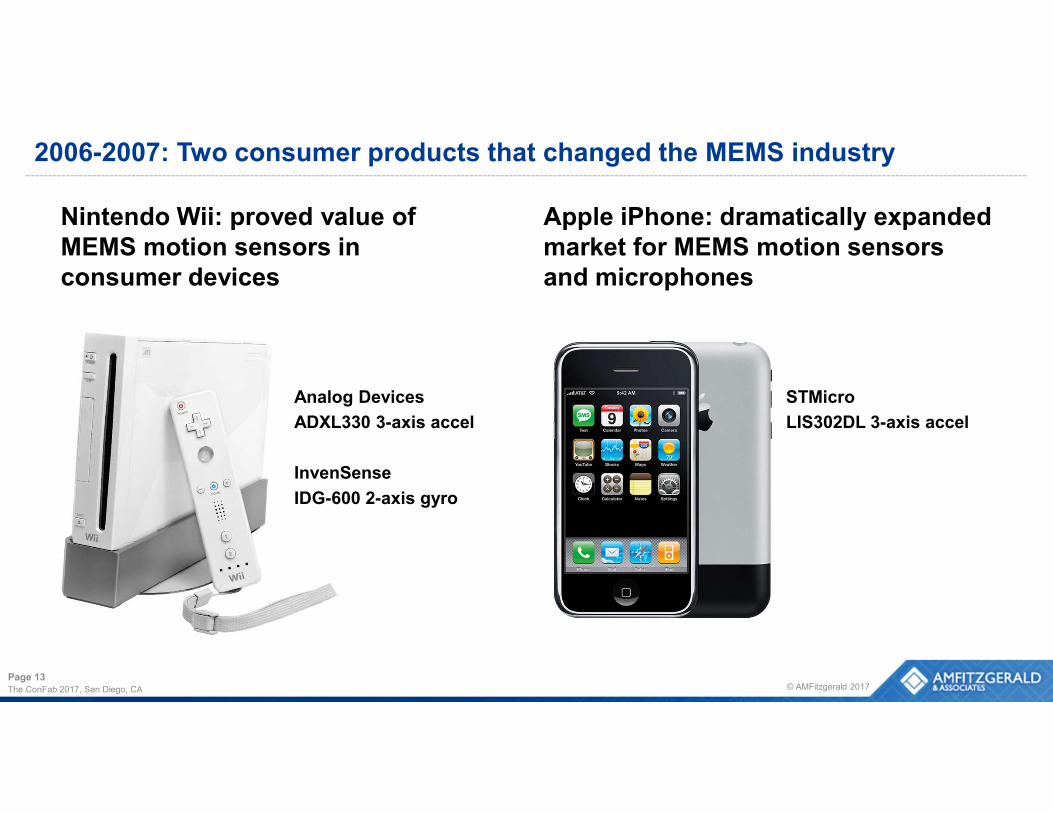
2006-2007: Two consumer products that changed the MEMS industry
Nintendo Wii: proved value of MEMS motion sensors in consumer devices
Apple iPhone: dramatically expanded market for MEMS motion sensors and microphones
The ConFab 2017, San Diego, CA © AMFitzgerald 2017Page 13
Analog Devices
ADXL330 3-axis accel
InvenSense
IDG-600 2-axis gyro
STMicro
LIS302DL 3-axis accel
2000s-2010s MEMS Technology
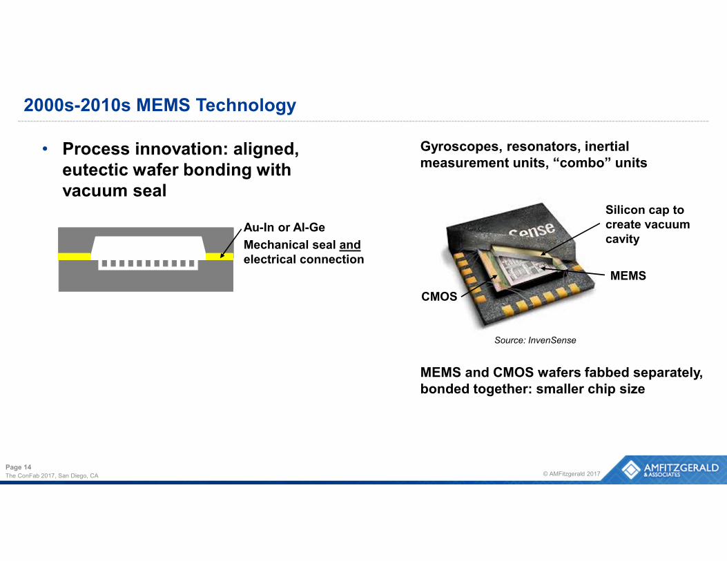
• Process innovation: aligned, eutectic wafer bonding with vacuum seal
The ConFab 2017, San Diego, CA © AMFitzgerald 2017Page 14
Au-In or Al-Ge
Mechanical seal and electrical connection
Silicon cap to create vacuum cavity
CMOS
MEMS
MEMS and CMOS wafers fabbed separately, bonded together: smaller chip size
Gyroscopes, resonators, inertial measurement units, “combo” units
Source: InvenSense

Seven years later: MEMS market transformed
The ConFab 2017, San Diego, CA © AMFitzgerald 2017Page 15
Winners: companies having MEMS for smartphones
Lexmark – off the chart
Epson – last place
90s-00s tech
80s-90s tech
00s-10s tech, from the Long Tail
Early adopters of next gen MEMS manufacturing became the big winners
• Big risks, big payoffs
– STMicroelectronics builds the first dedicated 200mm MEMS fab in 2005
– Bosch opens its 200mm MEMS fab in 2010, not too late
• Dedicated MEMS fabs helped give ST and Bosch market power
– Freedom to innovate without CMOS material restrictions
– Quickly expanded product lines
The ConFab 2017, San Diego, CA © AMFitzgerald 2017Page 16
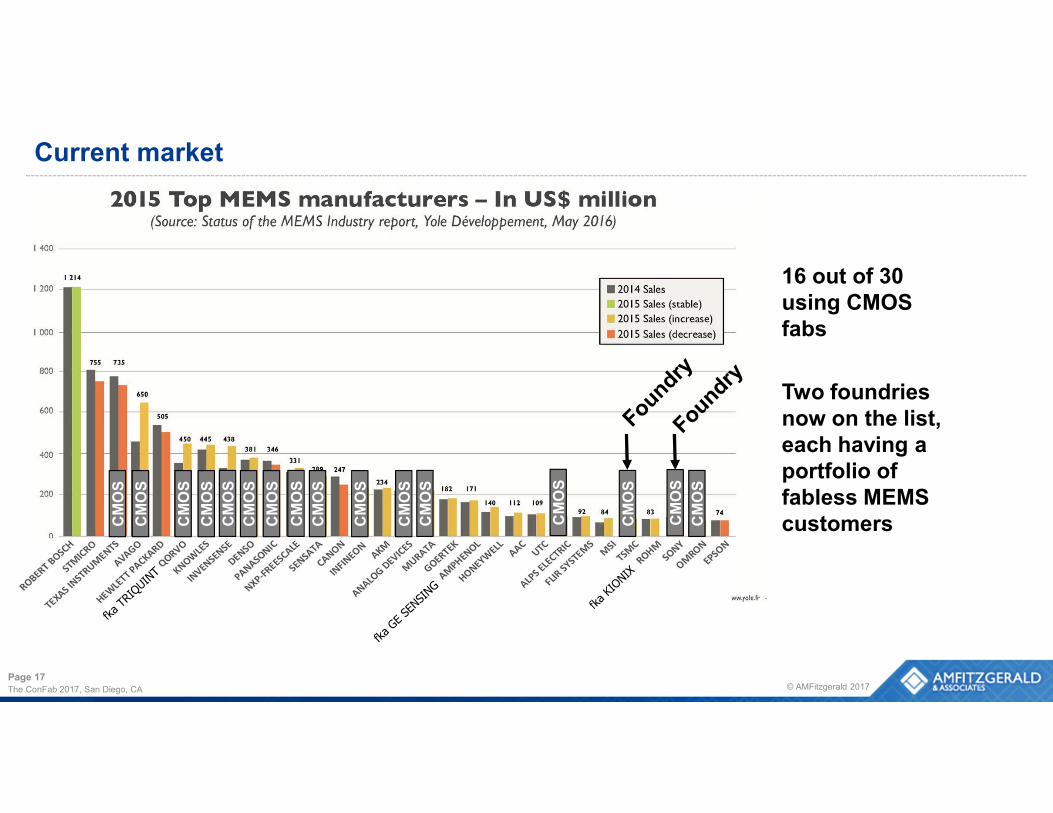
Current market
The ConFab 2017, San Diego, CA © AMFitzgerald 2017Page 17
16 out of 30 using CMOS fabs
Two foundries now on the list, each having a portfolio of fabless MEMS customersC
MO
S
CM
OS
CM
OS
CM
OS
CM
OS
CM
OS
CM
OS
CM
OS
CM
OS
CM
OS
CM
OS
CM
OS
CM
OS
CM
OS
CM
OS
CM
OS
MEMS retrospective insights
• Process innovation drives MEMS device innovation
• CMOS fabs have played a key role in MEMS since the 1990s
– Semiconductor industry infrastructure needed to meet end-user demands for cost, volume, and quality
• Today: MEMS + high volume → 200mm and CMOS-compatibility
– Unless you have your own captive MEMS fab
• New entrants come from the Long Tail, with new technology
The ConFab 2017, San Diego, CA © AMFitzgerald 2017Page 18
Next Generation MEMS, 2010-“MEMS Millennials”
Next generation MEMS are coming from academia, not industrial R&D
• Most new MEMS devices are being developed in research facilities, where process freedom exists
• New designs leverage new materials and processes
– Many innovations were not developed with CMOS-compatibility in mind
• Technology commercialization path: startup company or spin-out
• Meanwhile, most IDMs have been expanding their product lines through M&A, not research
The ConFab 2017, San Diego, CA © AMFitzgerald 2017Page 20

Next generation: Piezoelectric (PZT) MEMS
• Wide range of sensors and actuators possible using piezoelectrics
– AlN resonators and microphones established, due to CMOS-compatibility
• Process innovation: significant recent advances in thin film PZT deposition tools
• Major interest in PZT for superior d33 compared to AlN
– PZT is not CMOS-compatible
The ConFab 2017, San Diego, CA © AMFitzgerald 2017Page 21
Source: AMFitzgerald
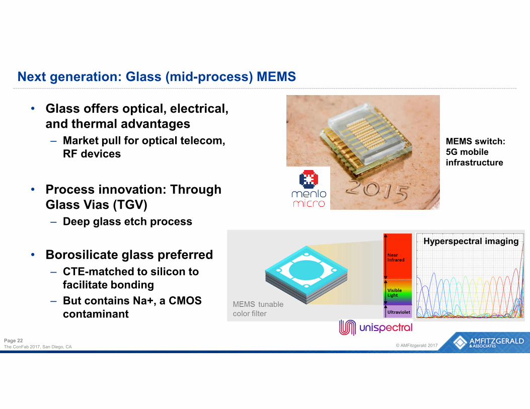
Next generation: Glass (mid-process) MEMS
• Glass offers optical, electrical, and thermal advantages
– Market pull for optical telecom, RF devices
• Process innovation: Through Glass Vias (TGV)
– Deep glass etch process
• Borosilicate glass preferred
– CTE-matched to silicon to facilitate bonding
– But contains Na+, a CMOS contaminant
The ConFab 2017, San Diego, CA © AMFitzgerald 2017Page 22
MEMS switch: 5G mobile infrastructure
Hyperspectral imaging
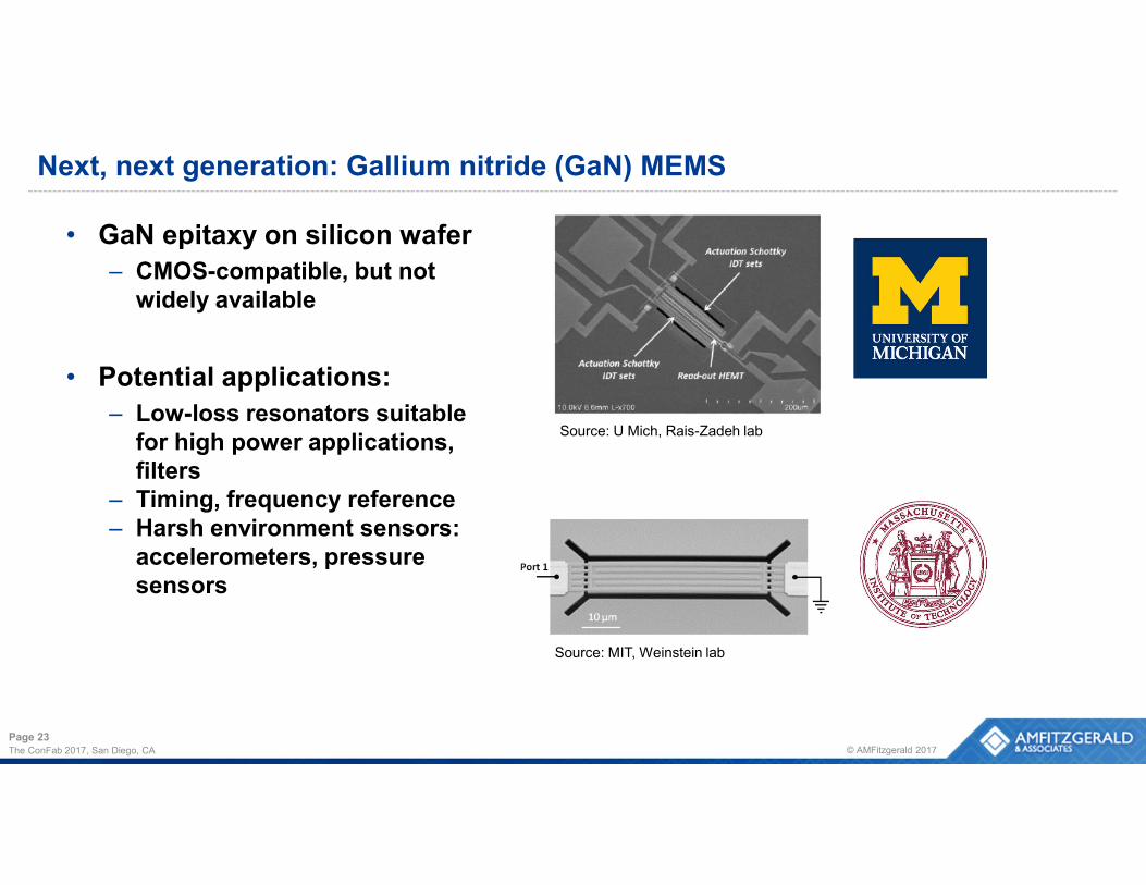
• GaN epitaxy on silicon wafer
– CMOS-compatible, but not widely available
• Potential applications:
– Low-loss resonators suitable for high power applications, filters
– Timing, frequency reference– Harsh environment sensors:
accelerometers, pressure sensors
Next, next generation: Gallium nitride (GaN) MEMS
The ConFab 2017, San Diego, CA © AMFitzgerald 2017
Page 23
Source: U Mich, Rais-Zadeh lab
Source: MIT, Weinstein lab
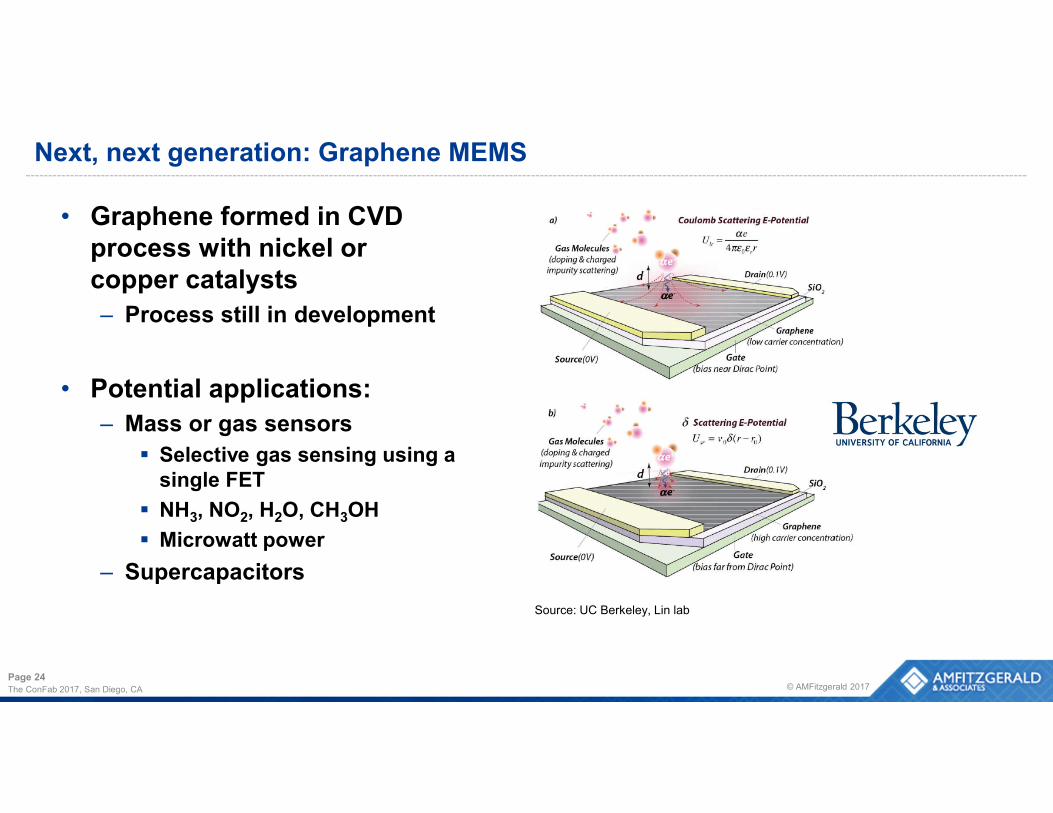
Next, next generation: Graphene MEMS
The ConFab 2017, San Diego, CA © AMFitzgerald 2017Page 24
Source: UC Berkeley, Lin lab
• Graphene formed in CVD process with nickel or copper catalysts
– Process still in development
• Potential applications:
– Mass or gas sensors
Selective gas sensing using a single FET
NH3, NO2, H2O, CH3OH
Microwatt power
– Supercapacitors
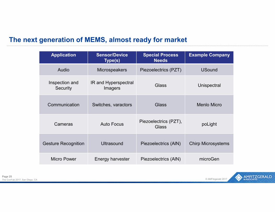
The next generation of MEMS, almost ready for market
Application Sensor/DeviceType(s)
Special Process Needs
Example Company
Audio Microspeakers Piezoelectrics (PZT) USound
Inspection and Security
IR and HyperspectralImagers
Glass Unispectral
Communication Switches, varactors Glass Menlo Micro
Cameras Auto FocusPiezoelectrics (PZT),
GlasspoLight
Gesture Recognition Ultrasound Piezoelectrics (AlN) Chirp Microsystems
Micro Power Energy harvester Piezoelectrics (AlN) microGen
The ConFab 2017, San Diego, CA © AMFitzgerald 2017Page 25
The smartphone (and consumer electronics) is still the ‘killer app’
• Next generation MEMS devices are aiming for the smartphone
– Still the obvious high volume market
• Next generation MEMS startup companies are fabless
– Investors don’t pay to build fabs!
• Access to high volume 200mm foundries will be key to scaling the business
– Apple, Samsung, etc. won’t tolerate smaller suppliers
The ConFab 2017, San Diego, CA © AMFitzgerald 2017Page 26
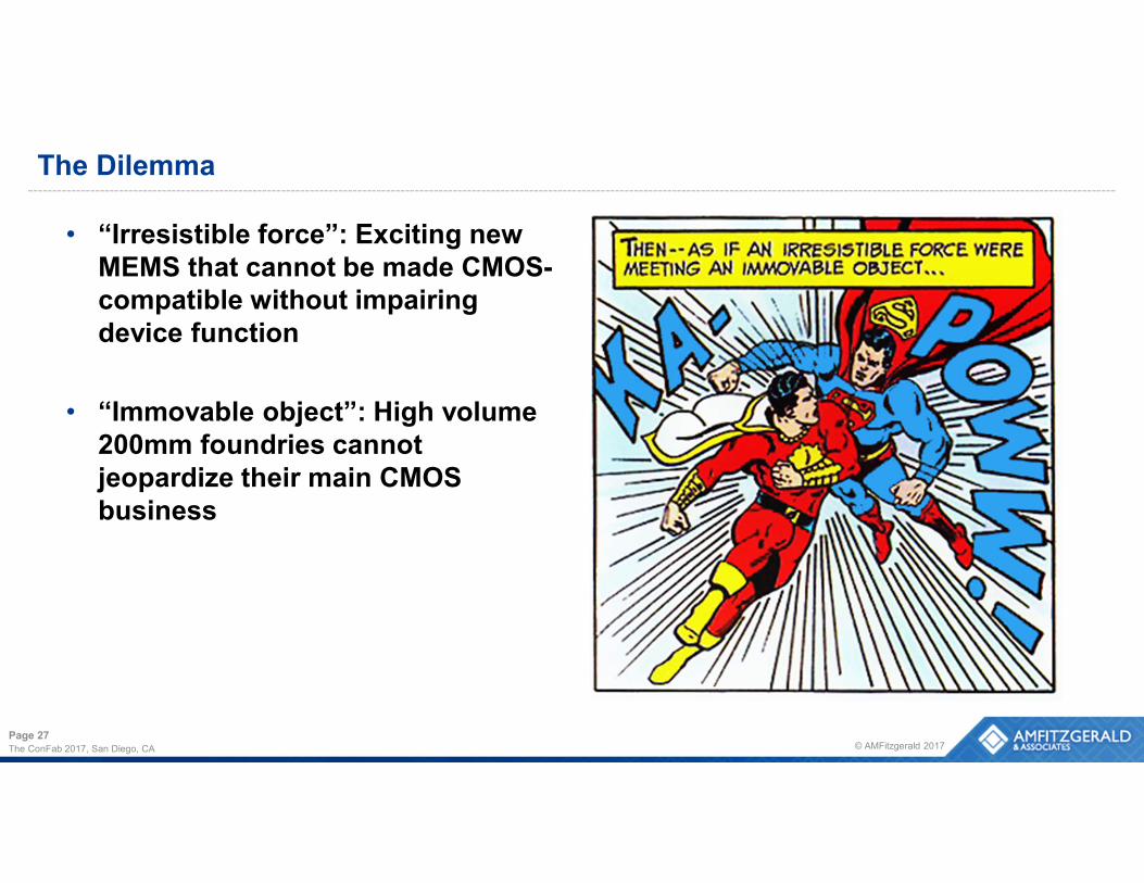
The Dilemma
• “Irresistible force”: Exciting new MEMS that cannot be made CMOS-compatible without impairing device function
• “Immovable object”: High volume 200mm foundries cannot jeopardize their main CMOS business
The ConFab 2017, San Diego, CA © AMFitzgerald 2017Page 27
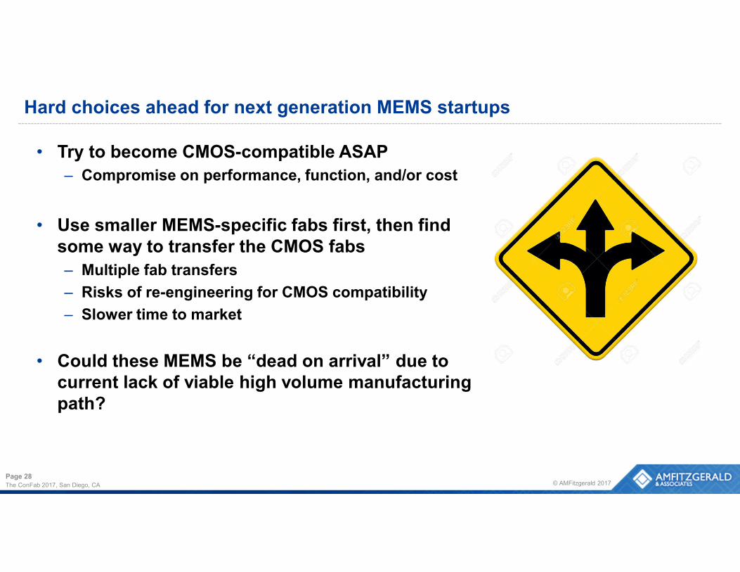
Hard choices ahead for next generation MEMS startups
• Try to become CMOS-compatible ASAP
– Compromise on performance, function, and/or cost
• Use smaller MEMS-specific fabs first, then find some way to transfer the CMOS fabs
– Multiple fab transfers
– Risks of re-engineering for CMOS compatibility
– Slower time to market
• Could these MEMS be “dead on arrival” due to current lack of viable high volume manufacturing path?
The ConFab 2017, San Diego, CA © AMFitzgerald 2017Page 28

Hard choices ahead for CMOS fabs
• Stick to CMOS-compatible
– Miss out on the next big opportunities in MEMS
– Existing MEMS business will become increasingly commoditized as technology ages
• Build MEMS-specific fabs
– (Or repurpose existing 200mm semiconductor fabs)
• Find ways to manage risks of handling non-CMOS materials mid-process
– Can equipment makers help find a solution?
The ConFab 2017, San Diego, CA © AMFitzgerald 2017Page 29
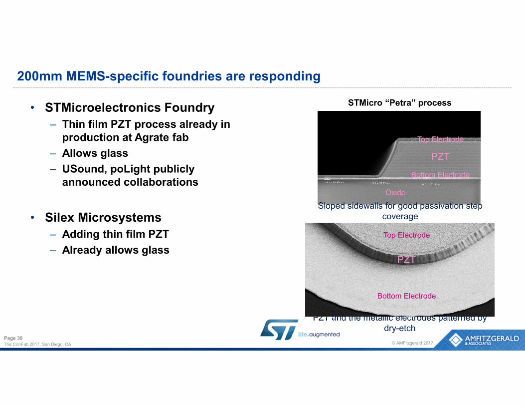
PZT and the metallic electrodes patterned by dry-etch
200mm MEMS-specific foundries are responding
• STMicroelectronics Foundry
– Thin film PZT process already in production at Agrate fab
– Allows glass
– USound, poLight publicly announced collaborations
• Silex Microsystems
– Adding thin film PZT
– Already allows glass
The ConFab 2017, San Diego, CA © AMFitzgerald 2017Page 30
Top Electrode
Bottom Electrode
PZT
PZT
Top Electrode
Bottom Electrode
Oxide
Sloped sidewalls for good passivation step coverage
STMicro “Petra” process
Call to Action and Summary
• Next generation, fabless MEMS companies are seeking development on 200mm to serve high volume markets
• High volume foundries must consider adopting new processes or miss out on emerging MEMS opportunities
• The field is starting to move already. How will you find a path forward?
Contact: [email protected]
The ConFab 2017, San Diego, CA © AMFitzgerald 2017Page 31