Embed Size (px)
Citation preview

1
New New New New LEDLEDLEDLED Lighting Lighting Lighting Lighting IPDIPDIPDIPD
MIP55MIP55MIP55MIP553333
ALMIGHTECH INTERNATIONAL (HK) CO.,Ltd
2nd Dev. group, Discrete Device Dev. Centre,
Semiconductor Company, Panasonic
Mr.Wang Mob:13631636755 TEL:0755-33009588

Example of application circuit
Reference data (When LED12pcs load in series is driven)
VAC = 120V , VLED = 28.6V , ILED = 0.390A , Po = 11.1W , Pin = 13.0W
ηηηη= 85.8% , pF = 0.93
LED current can be adjusted by the constant L2, RCL and REX.
However, the efficiency and PF will change, so please confirm.
“High efficiency and high PF is
achieved with low component count”
Components::::16
ηηηη=85.8%, PF=0.93
CVDD
1uF
CEX
1000pF
~~~~
F1
250VAC
1A MIP553IC1
REX
33kΩ
C2
0.1uF
400V
C1
0.1uF
400V
RCL
820kΩ
FRD1
600V/1.5A
L1
1000uH
FRD2
600V/1.5A L2
680uH
+
LED
Cout
10uF/50V
VIN D
S
CL
EX
VDD
BD
600V/1A
CCL
1000pF
9pcs in series
Effective for low output voltage specification and high efficiency
FRD3
600V/1.5A
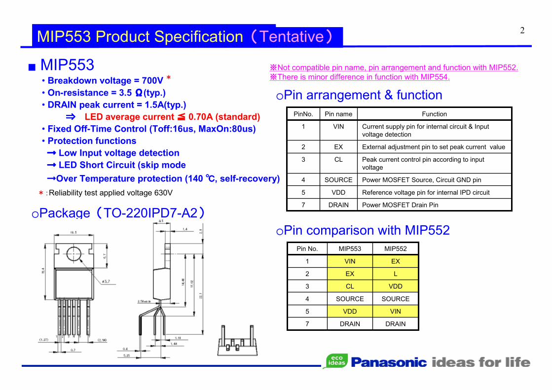
2MIP553 Product Specification(Tentative)
MIP553• Breakdown voltage = 700V
• On-resistance = 3.5 ΩΩΩΩ(typ.)
• DRAIN peak current = 1.5A(typ.)
⇒⇒⇒⇒ LED average current ≦≦≦≦ 0.70A (standard)
• Fixed Off-Time Control (Toff:16us, MaxOn:80us)
• Protection functions
→→→→ Low Input voltage detection
→→→→ LED Short Circuit (skip mode
→Over Temperature protection (140 , self-recovery)
Pin comparison with MIP552
Peak current control pin according to input
voltage
CL3
Power MOSFET Source, Circuit GND pinSOURCE4
Reference voltage pin for internal IPD circuitVDD5
External adjustment pin to set peak current valueEX2
Power MOSFET Drain PinDRAIN7
Current supply pin for internal circuit & Input
voltage detection
VIN1
FunctionPin namePinNo.
Pin arrangement & function
Package(TO-220IPD7-A2)
※Not compatible pin name, pin arrangement and function with MIP552.
※There is minor difference in function with MIP554.
VDDCL3
SOURCESOURCE4
VINVDD5
LEX2
DRAINDRAIN7
EXVIN1
MIP552MIP553Pin No.
*:Reliability test applied voltage 630V
*
3MIP553 vs MIP552 Characteristics Comparison
5.8V6.5VVDD(ON)
>45V
Low input voltage detection function
by VIN pin
>24V
Driving input voltage
1.0A1.5AILIMIT
ILIMIT is adjusted by voltage
Remote on/off function・・for PWM dimmer
ILIMIT is adjusted by current
Remote on/off function・・for PWM dimmerEX terminal function
-ILIMIT is adjusted by current
For simple PFC or TRIAC dimmer
CL terminal function
(Modified from L terminal
function of MIP552)
Over temperature protection:140(self recovery 70)
LED short protection(skip mode)
Over temperature protection:140(self recovery 70)
LED short protection(skip mode)
Protection function
6.0Ω3.5ΩRon
PWM control (44kHz)Fix OFF time (16us)Control method
MIP552MIP553Items
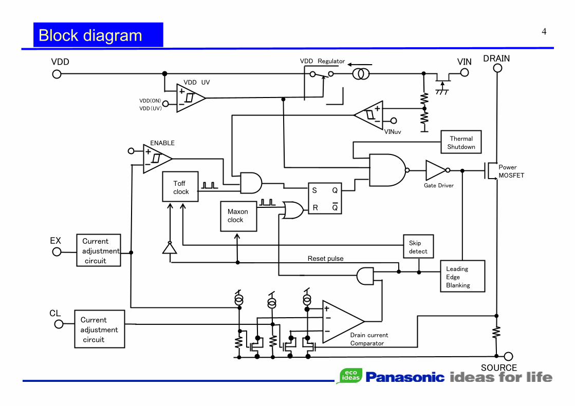
4Block diagram
SOURCE
DRAINVDD
R
S Q
Q
Gate Driver
PowerMOSFET
CL
VDD Regulator
VDD UV
EX
VDD(UV)
VDD(ON)
Toff
clock
Reset pulse
Thermal Shutdown
LeadingEdgeBlanking
Currentadjustmentcircuit
VIN
Currentadjustmentcircuit
Maxon
clock
ENABLE
Drain currentComparator
VINuv
Skipdetect
5
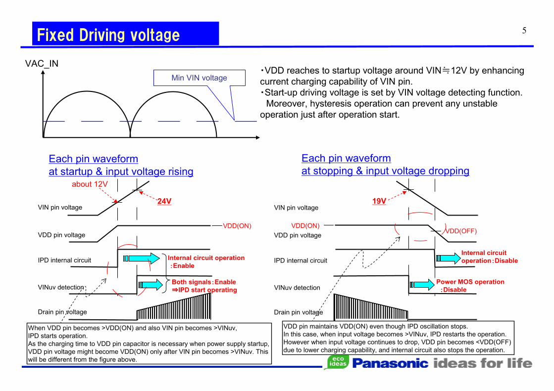
VAC_IN
Min VIN voltage・VDD reaches to startup voltage around VIN≒12V by enhancing
current charging capability of VIN pin.
・Start-up driving voltage is set by VIN voltage detecting function.Moreover, hysteresis operation can prevent any unstable
operation just after operation start.
VIN pin voltage
VDD pin voltage
IPD internal circuit
VINuv detection
Drain pin voltage
about 12V
24V
VDD(ON)
Internal circuit operation
::::Enable
Both signals::::Enable
⇒⇒⇒⇒IPD start operating
Each pin waveform
at startup & input voltage rising
Each pin waveform
at stopping & input voltage dropping
VIN pin voltage
VDD pin voltage
IPD internal circuit
VINuv detection
Drain pin voltage
19V
VDD(ON)
Internal circuit
operation::::Disable
Power MOS operation
::::Disable
VDD(OFF)
VDD pin maintains VDD(ON) even though IPD oscillation stops.
In this case, when input voltage becomes >VINuv, IPD restarts the operation.
However when input voltage continues to drop, VDD pin becomes <VDD(OFF)
due to lower charging capability, and internal circuit also stops the operation.
When VDD pin becomes >VDD(ON) and also VIN pin becomes >VINuv,
IPD starts operation.
As the charging time to VDD pin capacitor is necessary when power supply startup,
VDD pin voltage might become VDD(ON) only after VIN pin becomes >VINuv. This
will be different from the figure above.
Fixed Driving voltage
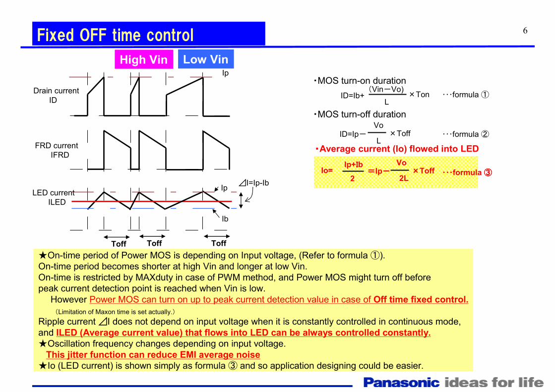
6Fixed OFF time control
Drain current
ID
FRD current
IFRD
LED current
ILED
Toff Toff Toff
High Vin Low VinIp
Ip
Ib
⊿I=Ip-Ib
・MOS turn-on duration
ID=Ib+L
(Vin-Vo)×Ton
・MOS turn-off duration
ID=Ip-L
Vo×Toff
・・・・Average current (Io) flowed into LED
Io=2L
Vo××××Toff====Ip----
Ip+IIIIb
2
・・・formula ①
・・・formula ②
・・・・・・・・・・・・formula ③③③③
On-time period of Power MOS is depending on Input voltage, (Refer to formula ①).
On-time period becomes shorter at high Vin and longer at low Vin.
On-time is restricted by MAXduty in case of PWM method, and Power MOS might turn off before
peak current detection point is reached when Vin is low.
However Power MOS can turn on up to peak current detection value in case of Off time fixed control.
(Limitation of Maxon time is set actually.)
Ripple current ⊿I does not depend on input voltage when it is constantly controlled in continuous mode,
and ILED (Average current value) that flows into LED can be always controlled constantly.
Oscillation frequency changes depending on input voltage.
This jitter function can reduce EMI average noise
Io (LED current) is shown simply as formula ③ and so application designing could be easier.
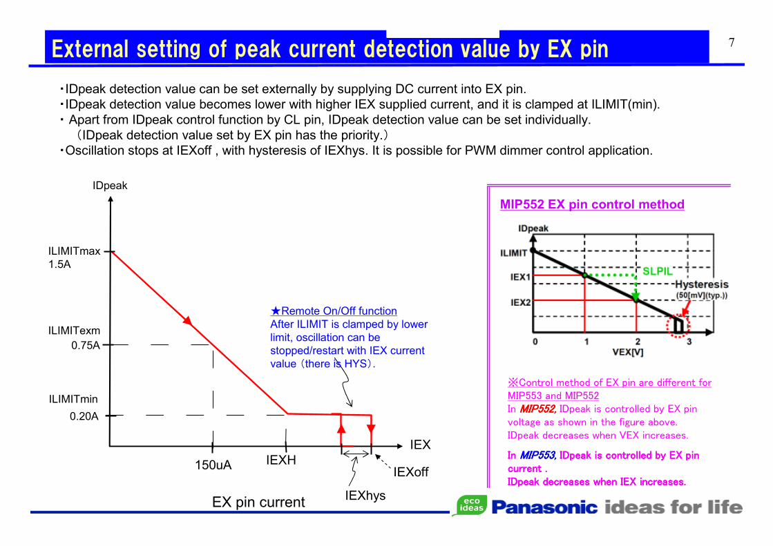
7
MIP552 EX pin control method
※Control method of EX pin are different for MIP553 and MIP552In MIP552,MIP552,MIP552,MIP552, IDpeak is controlled by EX pin voltage as shown in the figure above. IDpeak decreases when VEX increases.
In In In In MIP553,MIP553,MIP553,MIP553, IDpeakIDpeakIDpeakIDpeak is controlled by EX pin is controlled by EX pin is controlled by EX pin is controlled by EX pin current .current .current .current .IDpeakIDpeakIDpeakIDpeak decreases when IEX increases.decreases when IEX increases.decreases when IEX increases.decreases when IEX increases.
External setting of peak current detection value by EX pin
EX pin current
ILIMITmax
1.5A
0.75A
150uA
IDpeak
IEXH
0.20A
ILIMITmin
ILIMITexm
IEXoff
Remote On/Off function
After ILIMIT is clamped by lower
limit, oscillation can be
stopped/restart with IEX current
value (there is HYS).
IEXhys
IEX
・IDpeak detection value can be set externally by supplying DC current into EX pin.・IDpeak detection value becomes lower with higher IEX supplied current, and it is clamped at ILIMIT(min).・ Apart from IDpeak control function by CL pin, IDpeak detection value can be set individually.
(IDpeak detection value set by EX pin has the priority.)・Oscillation stops at IEXoff , with hysteresis of IEXhys. It is possible for PWM dimmer control application.
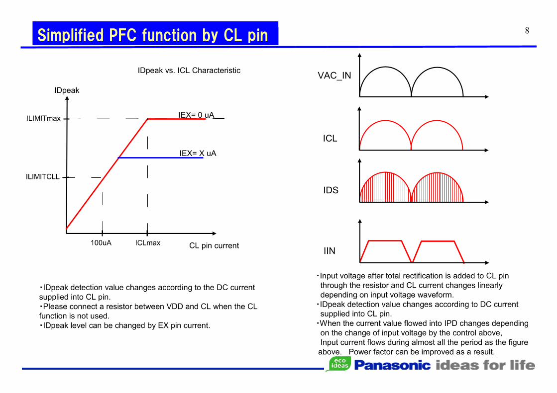
8Simplified PFC function by CL pin
CL pin current
ILIMITmax
IDpeak
IDpeak vs. ICL Characteristic
ICLmax
・IDpeak detection value changes according to the DC current supplied into CL pin.
・Please connect a resistor between VDD and CL when the CL function is not used.
・IDpeak level can be changed by EX pin current.
100uA
ILIMITCLL
IEX= 0 uA
IEX= X uA
VAC_IN
ICL
IDS
IIN
・Input voltage after total rectification is added to CL pin through the resistor and CL current changes linearly
depending on input voltage waveform.
・IDpeak detection value changes according to DC current supplied into CL pin.
・When the current value flowed into IPD changes depending on the change of input voltage by the control above,
Input current flows during almost all the period as the figure
above. Power factor can be improved as a result.
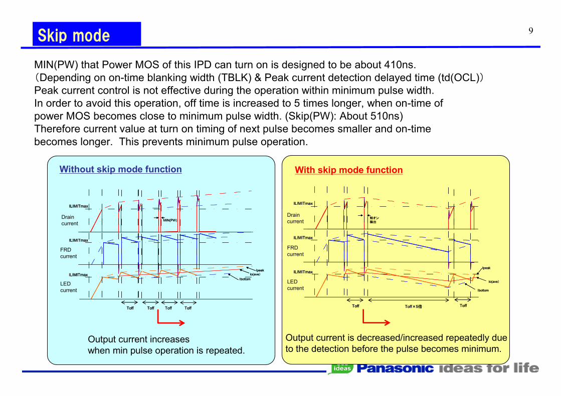
9Skip mode
ドレイン電流
FRD電流
ILIMITmax
LED電流
ILIMITmax
Ibottom
Ipeak
Io(ave)
短オン検出
Toff ToffToff×5倍
ILIMITmax
ドレイン電流
FRD電流
ILIMITmax
LED電流
ILIMITmax
Ibottom
Ipeak
Io(ave)
短オン検出
Toff ToffToff×5倍
ILIMITmax
Without skip mode function With skip mode function
MIN(PW) that Power MOS of this IPD can turn on is designed to be about 410ns.
(Depending on on-time blanking width (TBLK) & Peak current detection delayed time (td(OCL))Peak current control is not effective during the operation within minimum pulse width.
In order to avoid this operation, off time is increased to 5 times longer, when on-time of
power MOS becomes close to minimum pulse width. (Skip(PW): About 510ns)
Therefore current value at turn on timing of next pulse becomes smaller and on-time
becomes longer. This prevents minimum pulse operation.
ドレイン電流
FRD電流
ILIMITmax
LED電流
MIN(PW)
ILIMITmax
Ibottom
Ipeak
Io(ave)
Toff Toff Toff Toff
ILIMITmax
ドレイン電流
FRD電流
ILIMITmax
LED電流
MIN(PW)
ILIMITmax
Ibottom
Ipeak
Io(ave)
Toff Toff Toff Toff
ILIMITmax
Drain
current
FRD
current
LED
current
Output current increases
when min pulse operation is repeated.
Drain
current
FRD
current
LED
current
Output current is decreased/increased repeatedly due
to the detection before the pulse becomes minimum.
10
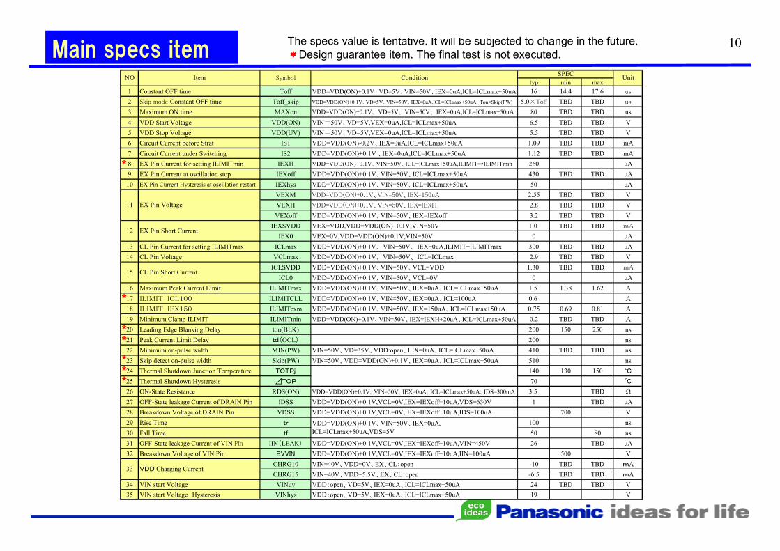
typ min max
1 Constant OFF time Toff VDD=VDD(ON)+0.1V、VD=5V、VIN=50V、IEX=0uA,ICL=ICLmax+50uA 16 14.4 17.6 us
2 Skip mode Constant OFF time Toff_skip VDD=VDD(ON)+0.1V、VD=5V、VIN=50V、IEX=0uA,ICL=ICLmax+50uA Ton<Skip(PW) 5.0×Toff TBD TBD us
3 Maximum ON time MAXon VDD=VDD(ON)+0.1V、VD=5V、VIN=50V、IEX=0uA,ICL=ICLmax+50uA 80 TBD TBD us
4 VDD Start Voltage VDD(ON) VIN=50V、VD=5V,VEX=0uA,ICL=ICLmax+50uA 6.5 TBD TBD V
5 VDD Stop Voltage VDD(UV) VIN=50V、VD=5V,VEX=0uA,ICL=ICLmax+50uA 5.5 TBD TBD V
6 Circuit Current before Strat IS1 VDD=VDD(ON)-0.2V、IEX=0uA,ICL=ICLmax+50uA 1.09 TBD TBD mA
7 Circuit Current under Switching IS2 VDD=VDD(ON)+0.1V 、IEX=0uA,ICL=ICLmax+50uA 1.12 TBD TBD mA
8 EX Pin Current for setting ILIMITmin IEXH VDD=VDD(ON)+0.1V、VIN=50V、ICL=ICLmax+50uA,ILIMIT⇒ILIMITmin 260 µA
9 EX Pin Current at oscillation stop IEXoff VDD=VDD(ON)+0.1V、VIN=50V、ICL=ICLmax+50uA 430 TBD TBD µA
10 EX Pin Current Hysteresis at oscillation restart IEXhys VDD=VDD(ON)+0.1V、VIN=50V、ICL=ICLmax+50uA 50 µA
VEXM VDD=VDD(ON)+0.1V、VIN=50V、IEX=150uA 2.55 TBD TBD V
VEXH VDD=VDD(ON)+0.1V、VIN=50V、IEX=IEXH 2.8 TBD TBD V
VEXoff VDD=VDD(ON)+0.1V、VIN=50V、IEX=IEXoff 3.2 TBD TBD V
IEXSVDD VEX=VDD,VDD=VDD(ON)+0.1V,VIN=50V 1.0 TBD TBD mA
IEX0 VEX=0V,VDD=VDD(ON)+0.1V,VIN=50V 0 µA
13 CL Pin Current for setting ILIMITmax ICLmax VDD=VDD(ON)+0.1V、VIN=50V、IEX=0uA,ILIMIT=ILIMITmax 300 TBD TBD µA
14 CL Pin Voltage VCLmax VDD=VDD(ON)+0.1V、VIN=50V、ICL=ICLmax 2.9 TBD TBD V
ICLSVDD VDD=VDD(ON)+0.1V、VIN=50V、VCL=VDD 1.30 TBD TBD mA
ICL0 VDD=VDD(ON)+0.1V、VIN=50V、VCL=0V 0 µA
16 Maximum Peak Current Limit ILIMITmax VDD=VDD(ON)+0.1V、VIN=50V、IEX=0uA、ICL=ICLmax+50uA 1.5 1.38 1.62 A
17 ILIMIT ICL100 ILIMITCLL VDD=VDD(ON)+0.1V、VIN=50V、IEX=0uA、ICL=100uA 0.6 A
18 ILIMIT IEX150 ILIMITexm VDD=VDD(ON)+0.1V、VIN=50V、IEX=150uA、ICL=ICLmax+50uA 0.75 0.69 0.81 A
19 Minimum Clamp ILIMIT ILIMITmin VDD=VDD(ON)+0.1V、VIN=50V、IEX=IEXH+20uA、ICL=ICLmax+50uA 0.2 TBD TBD A
20 Leading Edge Blanking Delay ton(BLK) 200 150 250 ns
21 Peak Current Limit Delay td(OCL) 200 ns
22 Minimum on-pulse width MIN(PW) VIN=50V、VD=35V、VDD:open、IEX=0uA、ICL=ICLmax+50uA 410 TBD TBD ns
23 Skip detect on-pulse width Skip(PW) VIN=50V、VDD=VDD(ON)+0.1V、IEX=0uA、ICL=ICLmax+50uA 510 ns
24 Thermal Shutdown Junction Temperature TOTPj 140 130 150
25 Thermal Shutdown Hysteresis ⊿TOP 70
26 ON-State Resistance RDS(ON) VDD=VDD(ON)+0.1V、VIN=50V、IEX=0uA、ICL=ICLmax+50uA、IDS=300mA 3.5 TBD Ω
27 OFF-State leakage Current of DRAIN Pin IDSS VDD=VDD(ON)+0.1V,VCL=0V,IEX=IEXoff+10uA,VDS=630V 1 TBD µA
28 Breakdown Voltage of DRAIN Pin VDSS VDD=VDD(ON)+0.1V,VCL=0V,IEX=IEXoff+10uA,IDS=100uA 700 V
29 Rise Time tr 100 ns
30 Fall Time tf 50 80 ns
31 OFF-State leakage Current of VIN Pin IIN(LEAK) VDD=VDD(ON)+0.1V,VCL=0V,IEX=IEXoff+10uA,VIN=450V 26 TBD µA
32 Breakdown Voltage of VIN Pin BVVIN VDD=VDD(ON)+0.1V,VCL=0V,IEX=IEXoff+10uA,IIN=100uA 500 V
CHRG10 VIN=40V、VDD=0V、EX、CL:open -10 TBD TBD mA
CHRG15 VIN=40V、VDD=5.5V、EX、CL:open -6.5 TBD TBD mA
34 VIN start Voltage VINuv VDD:open、VD=5V、IEX=0uA、ICL=ICLmax+50uA 24 TBD TBD V
35 VIN start Voltage Hysteresis VINhys VDD:open、VD=5V、IEX=0uA、ICL=ICLmax+50uA 19 V
33
12
Unit
VDD Charging Current
VDD=VDD(ON)+0.1V、VIN=50V、IEX=0uA,
ICL=ICLmax+50uA,VDS=5V
EX Pin Voltage11
EX Pin Short Current
CL Pin Short Current15
NO ConditionSPEC
SymbolItem
Main specs itemThe specs value is tentative. It will be subjected to change in the future.
****Design guarantee item. The final test is not executed.
*
*
**
***
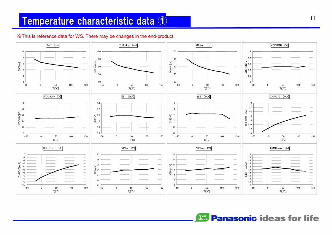
11Temperature characteristic data ①
※This is reference data for WS. There may be changes in the end-product.
Toff [us]
10
12
14
16
18
20
-50 0 50 100 150
Tj[]
Toff
[us]
Toff_skip [us]
60
70
80
90
100
-50 0 50 100 150
Tj[]
Toff
_ski
p[u
s]
MAXon [us]
60
70
80
90
100
-50 0 50 100 150
Tj[]
MA
Xon[u
s]
VDD(ON) [V]
6
6.2
6.4
6.6
6.8
7
-50 0 50 100 150
Tj[]
VD
D(O
N)[
V]
VDD(UV) [V]
5
5.2
5.4
5.6
5.8
6
-50 0 50 100 150
Tj[]
VD
D(U
V)[
V]
IS1 [mA]
0.8
0.9
1
1.1
1.2
1.3
-50 0 50 100 150
Tj[]
IS1[
mA
]IS2 [mA]
0.8
0.9
1
1.1
1.2
1.3
-50 0 50 100 150
Tj[]
IS2[
mA
]
CHRG10 [mA]
-14
-12
-10
-8
-6
-4
-2
0
-50 0 50 100 150
Tj[]
CH
RG
10[m
A]
CHRG15 [mA]
-10
-9
-8
-7
-6
-5
-4
-3
-2
-1
0
-50 0 50 100 150
Tj[]
CH
RG
15[
mA
]
VINuv [V]
21
22
23
24
25
26
27
-50 0 50 100 150
Tj[]
VIN
uv[
V]
VINhys [V]
16
17
18
19
20
21
22
-50 0 50 100 150
Tj[]
VIN
hys
[V]
ILIMITmax [A]
1
1.1
1.2
1.3
1.4
1.5
1.6
1.7
1.8
1.9
2
-50 0 50 100 150
Tj[]
ILIM
ITm
ax[A
]
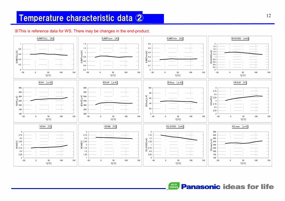
12Temperature characteristic data ②
ILIMITCLL [A]
0
0.2
0.4
0.6
0.8
1
-50 0 50 100 150
Tj[]
ILIM
ITC
LL[A
]
ILIMITexm [A]
0.2
0.4
0.6
0.8
1
1.2
1.4
-50 0 50 100 150
Tj[]
ILIM
ITexm
[A]
ILIMITmin [A]
0
0.1
0.2
0.3
0.4
0.5
0.6
-50 0 50 100 150
Tj[]
ILIM
ITm
in[A
]
IEXSVDD [mA]
0
0.2
0.4
0.6
0.8
1
1.2
1.4
1.6
1.8
2
-50 0 50 100 150
Tj[]
IEXSV
DD
[mA
]
IEXH [μA]
100
150
200
250
300
350
400
-50 0 50 100 150
Tj[]
IEXH
[μA
]
IEXoff [μA]
300
350
400
450
500
550
600
-50 0 50 100 150
Tj[]
IEXoff
[μA
]IEXhys [μA]
0
20
40
60
80
100
-50 0 50 100 150
Tj[]
IEXhys
[μA
]
VEXoff [V]
2
2.25
2.5
2.75
3
3.25
3.5
3.75
4
-50 0 50 100 150
Tj[]
VEXoff
[V]
VEXH [V]
2
2.25
2.5
2.75
3
3.25
3.5
3.75
4
-50 0 50 100 150
Tj[]
VEXH
[V]
VEXM [V]
1
1.25
1.5
1.75
2
2.25
2.5
2.75
3
-50 0 50 100 150
Tj[]
VEXM
[V]
ICLSVDD [mA]
0
0.25
0.5
0.75
1
1.25
1.5
1.75
2
-50 0 50 100 150
Tj[]
ICLSV
DD
[mA
]
ICLmax [μA]
100
150
200
250
300
350
400
450
500
-50 0 50 100 150
Tj[]
ICLm
ax[μ
A]
※This is reference data for WS. There may be changes in the end-product.
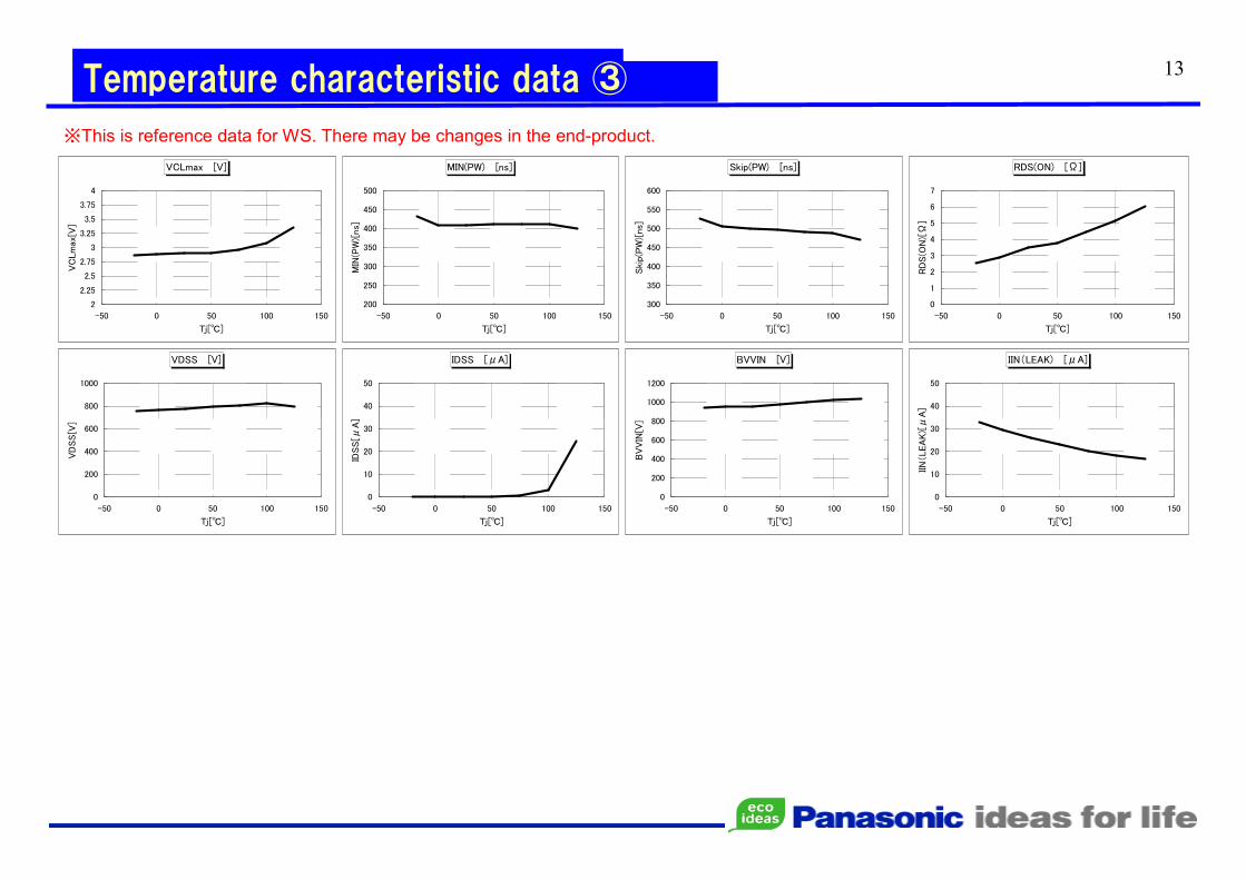
13Temperature characteristic data ③
VCLmax [V]
2
2.25
2.5
2.75
3
3.25
3.5
3.75
4
-50 0 50 100 150
Tj[]
VC
Lm
ax[V
]
MIN(PW) [ns]
200
250
300
350
400
450
500
-50 0 50 100 150
Tj[]
MIN
(PW
)[ns]
Skip(PW) [ns]
300
350
400
450
500
550
600
-50 0 50 100 150
Tj[]
Ski
p(P
W)[
ns]
RDS(ON) [Ω]
0
1
2
3
4
5
6
7
-50 0 50 100 150
Tj[]
RD
S(O
N)[
Ω]
VDSS [V]
0
200
400
600
800
1000
-50 0 50 100 150
Tj[]
VD
SS[V
]
IDSS [μA]
0
10
20
30
40
50
-50 0 50 100 150
Tj[]
IDSS[μ
A]
BVVIN [V]
0
200
400
600
800
1000
1200
-50 0 50 100 150
Tj[]
BV
VIN
[V]
IIN(LEAK) [μA]
0
10
20
30
40
50
-50 0 50 100 150
Tj[]
IIN(LEA
K)[
μA
]
※This is reference data for WS. There may be changes in the end-product.
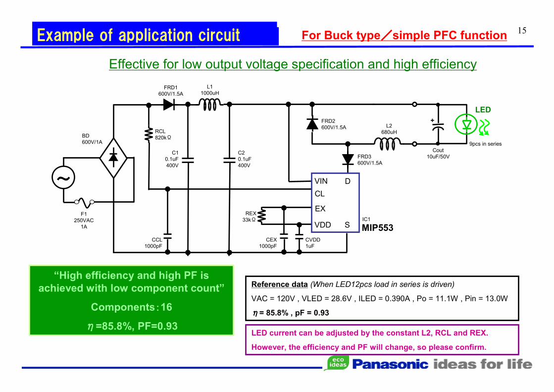
15Example of application circuit For Buck type////simple PFC function
Reference data (When LED12pcs load in series is driven)
VAC = 120V , VLED = 28.6V , ILED = 0.390A , Po = 11.1W , Pin = 13.0W
ηηηη= 85.8% , pF = 0.93
LED current can be adjusted by the constant L2, RCL and REX.
However, the efficiency and PF will change, so please confirm.
“High efficiency and high PF is
achieved with low component count”
Components::::16
ηηηη=85.8%, PF=0.93
CVDD
1uF
CEX
1000pF
~~~~
F1
250VAC
1A MIP553IC1
REX
33kΩ
C2
0.1uF
400V
C1
0.1uF
400V
RCL
820kΩ
FRD1
600V/1.5A
L1
1000uH
FRD2
600V/1.5A L2
680uH
+
LED
Cout
10uF/50V
VIN D
S
CL
EX
VDD
BD
600V/1A
CCL
1000pF
9pcs in series
Effective for low output voltage specification and high efficiency
FRD3
600V/1.5A

16
Reference data (When LED10pcs load in series is driven)
VAC = 120V , VLED = 28.4V , ILED = 0.379A , Po = 10.7W , Pin = 13.4W
ηηηη= 80.4% , pF = 0.95
““““High PF is achieved
with low component
count”
PF=0.95
~~~~
F1
250VAC
1A
MIP553
DB
600V/1A
FRD1
600V/1.5A
L1
1000uH
C2
0.1uF
400V
CVDD
1uF
CEX
1000pF
REX
56kΩ
+
IC1
C1
0.1uF
400V
VIN D
S
CL
EX
VDD
RCL
620kΩ
L2
680uH
Cout
10uF/50V
FRD2
600V/1.5A
LED
Buck-Boost Type////Simple PFC function
9pcs in series
CCL
1000pF
Effective for high output voltage specification and high PF
FRD3
600V/1.5A
LED current can be adjusted by the constant L2, RCL and REX.
However, the efficiency and PF will change, so please confirm.
Example of application circuit

17Buck-Boost Type////Simple PFC function
These components are necessary for smooth dimming
operation when connected to a TRIAC dimmer.
~~~~
F1
250VAC
1A
MIP553
DB
600V
1A
C2
0.1uF
400V
CVDD
1uF
CEX
1000pF
REX
56kΩ
Dimmer
LED
+
CCL
32uF
IC1
C1
0.1uF
400V
VIN D
S
CL
EX
VDD
RCL
470kΩ
L2
680uH
Rout
10kΩ/2W
Cout
10uF/50V
FRD2
600V / 1.5A
+
RDIM
11kΩ2W
CDIM
10uF
400V
FRD1
600V / 1.5A
L1
1000uH
For TRIAC dimmer(Reference circuit)
Please adjust the value of L2, RCL and REX when LED current is
increased.
Please adjust RCL, RDIM and CDIM to prevent malfunction of the
dimmer.
Moreover, a dummy resistor Rout is necessary to turn of the LED
during 0% dimmer.
“TRIAC dimmer is achieved
with low component count”
Components::::18
A dummy resistor is necessary
for turning off the LED during
0% dimmer
※Buck-Boost type is recommended for flicker-free dimming.
(The buck type will cause oscillation to occur during the stopping period
at low input condition)
Example of application circuit
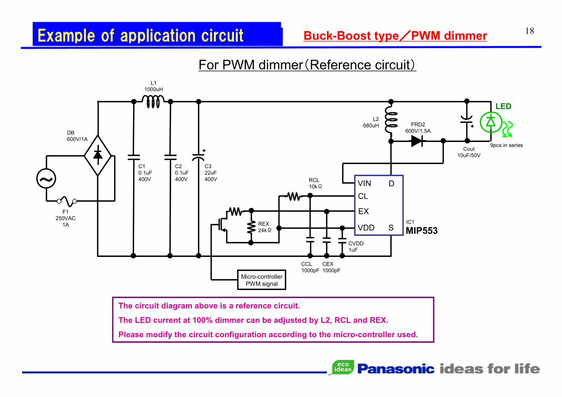
18Buck-Boost type////PWM dimmer
The circuit diagram above is a reference circuit.
The LED current at 100% dimmer can be adjusted by L2, RCL and REX.
Please modify the circuit configuration according to the micro-controller used.
For PWM dimmer(Reference circuit)
~~~~
F1
250VAC
1A
MIP553
DB
600V/1A
L1
1000uH
C2
0.1uF
400V
CVDD
1uF
CEX
1000pF
REX
24kΩ
+
IC1
VIN D
S
CL
EX
VDD
RCL
10kΩ
L2
680uH
Cout
10uF/50V
FRD2
600V/1.5A
LED
9pcs in series
Micro-controller
PWM signal
C1
0.1uF
400V
+
C3
22uF
400V
CCL
1000pF
Example of application circuit
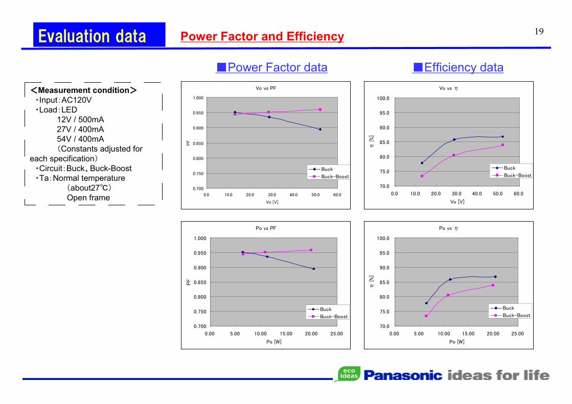
19Evaluation data Power Factor and Efficiency
Vo vs PF
0.700
0.750
0.800
0.850
0.900
0.950
1.000
0.0 10.0 20.0 30.0 40.0 50.0 60.0
Vo [V]
PF
Buck
Buck-Boost
Po vs PF
0.700
0.750
0.800
0.850
0.900
0.950
1.000
0.00 5.00 10.00 15.00 20.00 25.00
Po [W]
PF
Buck
Buck-Boost
Vo vs η
70.0
75.0
80.0
85.0
90.0
95.0
100.0
0.0 10.0 20.0 30.0 40.0 50.0 60.0
Vo [V]
η [
%]
Buck
Buck-Boost
Po vs η
70.0
75.0
80.0
85.0
90.0
95.0
100.0
0.00 5.00 10.00 15.00 20.00 25.00
Po [W]
η [
%]
Buck
Buck-Boost
Power Factor data Efficiency data
<<<<Measurement condition>>>>・Input:AC120V・Load:LED
12V / 500mA
27V / 400mA
54V / 400mA
(Constants adjusted for each specification)
・Circuit:Buck、Buck-Boost・Ta:Normal temperature
(about27)Open frame
20Evaluation data LED Current accuracy
<<<<Measurement condition>>>>・Input:AC120V・Load:LED 9pcs
27V / 400mA
・Circuit:BuckWithout input filter capacitor
・Ta:Normal Temperature(about 27)
Open frame
Temperature characteristic(※Confirmation of temperature effect on ILIMIT)
LED Current accuracy
Ta vs ILED
200
250
300
350
400
450
500
0 20 40 60 80 100
Ta []IL
ED
[m
A]
ILED=400mA
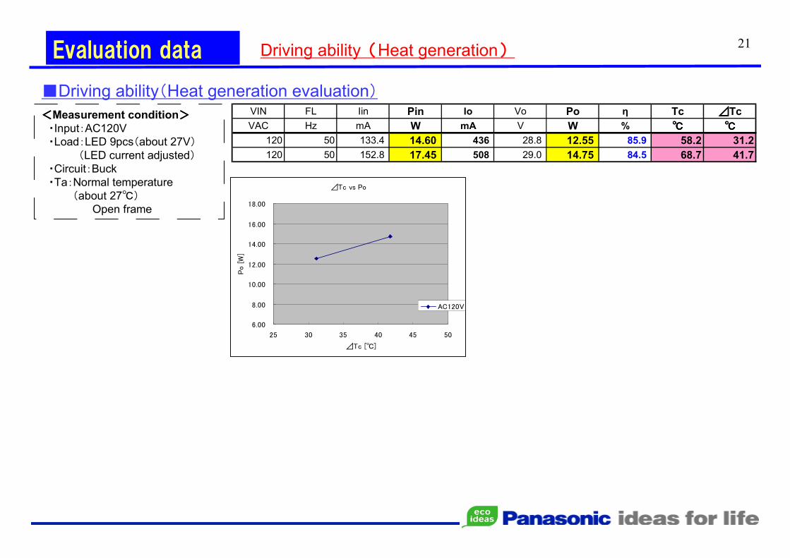
21Evaluation data Driving ability(Heat generation)
Driving ability(Heat generation evaluation)
<<<<Measurement condition>>>>・Input:AC120V・Load:LED 9pcs(about 27V)
(LED current adjusted)・Circuit:Buck・Ta:Normal temperature
(about 27)Open frame
VIN FL Iin Pin Io Vo Po η Tc ⊿⊿⊿⊿Tc
VAC Hz mA W mA V W %
120 50 133.4 14.60 436 28.8 12.55 85.9 58.2 31.2
120 50 152.8 17.45 508 29.0 14.75 84.5 68.7 41.7
⊿Tc vs Po
6.00
8.00
10.00
12.00
14.00
16.00
18.00
25 30 35 40 45 50
⊿Tc []
Po [
W]
AC120V
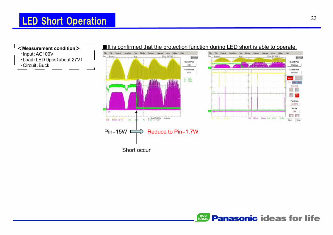
22LED Short Operation
<<<<Measurement condition>>>>・Input:AC100V・Load:LED 9pcs(about 27V)・Circuit:Buck
It is confirmed that the protection function during LED short is able to operate.
Pin=15W
Short occur
Reduce to Pin=1.7W
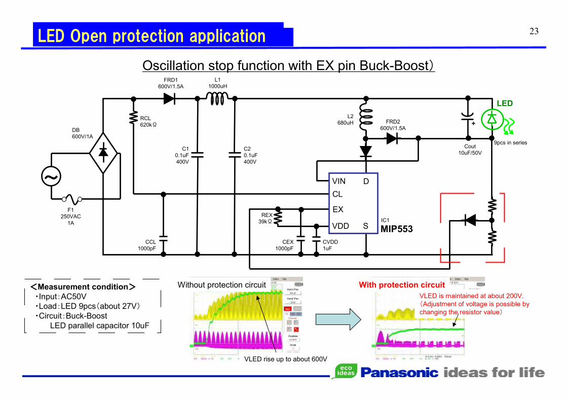
23LED Open protection application
~~~~
F1
250VAC
1A
MIP553
DB
600V/1A
FRD1
600V/1.5A
L1
1000uH
C2
0.1uF
400V
CVDD
1uF
CEX
1000pF
REX
39kΩ
+
IC1
C1
0.1uF
400V
VIN D
S
CL
EX
VDD
RCL
620kΩ
L2
680uH
Cout
10uF/50V
FRD2
600V/1.5A
LED
9pcs in series
CCL
1000pF
Oscillation stop function with EX pin Buck-Boost)
Without protection circuit With protection circuit
VLED rise up to about 600V
VLED is maintained at about 200V.
(Adjustment of voltage is possible by changing the resistor value)
<<<<Measurement condition>>>>・Input:AC50V・Load:LED 9pcs(about 27V)・Circuit:Buck-Boost
LED parallel capacitor 10uF

24Power supply design support tool
For the simplification of the external components design, such as the L value of the coil, CL resistance (RCL), EX resistance (REX), etc.,
a calculation sheet shown in the figure below has been prepared.
If the sheet is required, please contact us.
Mr.Wang Mob:13631636755 TEL:0755-33009588