Embed Size (px)
Citation preview
J. GrollierUnité Mixte de Physique CNRS/Thales
Palaiseau, France
Neuromorphic Computing
‐Memristors ‐
Nanobrain
Outline
1- memristor devices : introduction
2- memristors as digital memory
3- memristors for logic applications
4- memristors for neuromorphic computing
1
Outline
1- memristor devices : introduction
2- memristors as digital memory
3- memristors for logic applications
4- memristors for neuromorphic computing
1
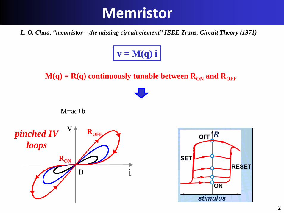
MemristorL. O. Chua, “memristor – the missing circuit element” IEEE Trans. Circuit Theory (1971)
v = M(q) i
pinched IV loops
M=aq+b
v
0
ROFF
RON
i
M(q) = R(q) continuously tunable between RON and ROFF
2
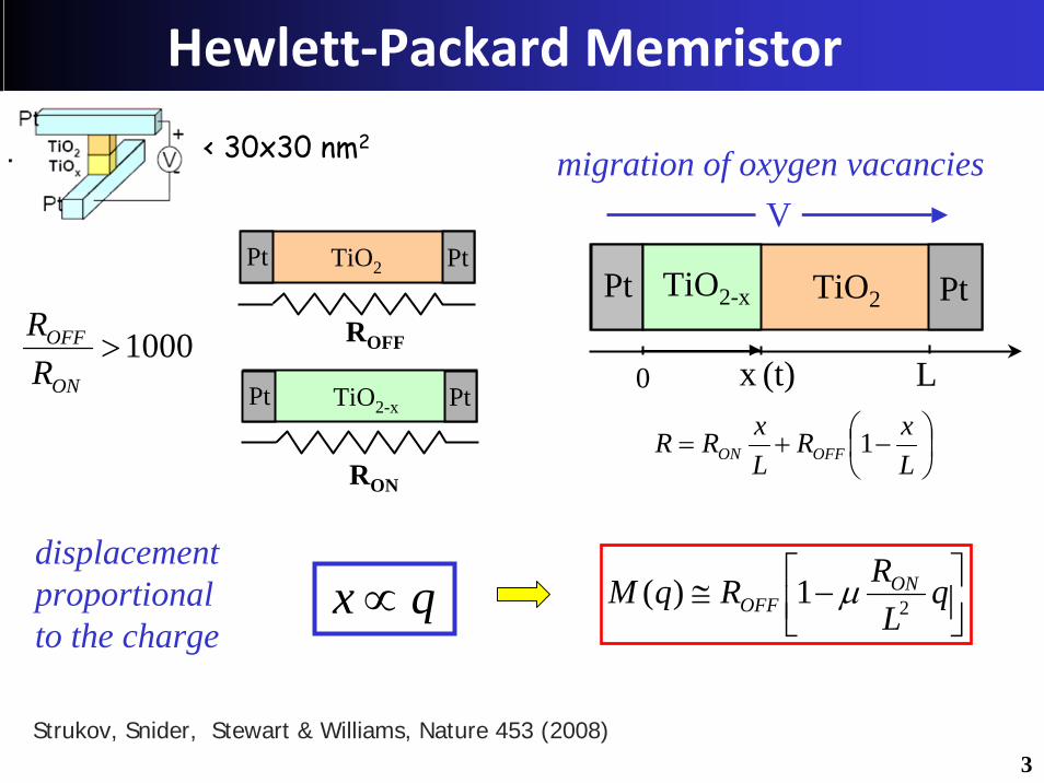
Hewlett‐Packard Memristor
Pt PtTiO2
ROFF
Pt PtTiO2-x
RON
qx ∝ ⎥⎦⎤
⎢⎣⎡ −≅ q
LRRqM ON
OFF 21)( μ
Pt PtTiO2-x TiO2
0 x (t) L
⎟⎠⎞
⎜⎝⎛ −+=
LxR
LxRR OFFON 1
V
displacement proportional to the charge
Strukov, Snider, Stewart & Williams, Nature 453 (2008)
migration of oxygen vacancies < 30x30 nm2
1000>ON
OFF
RR
3
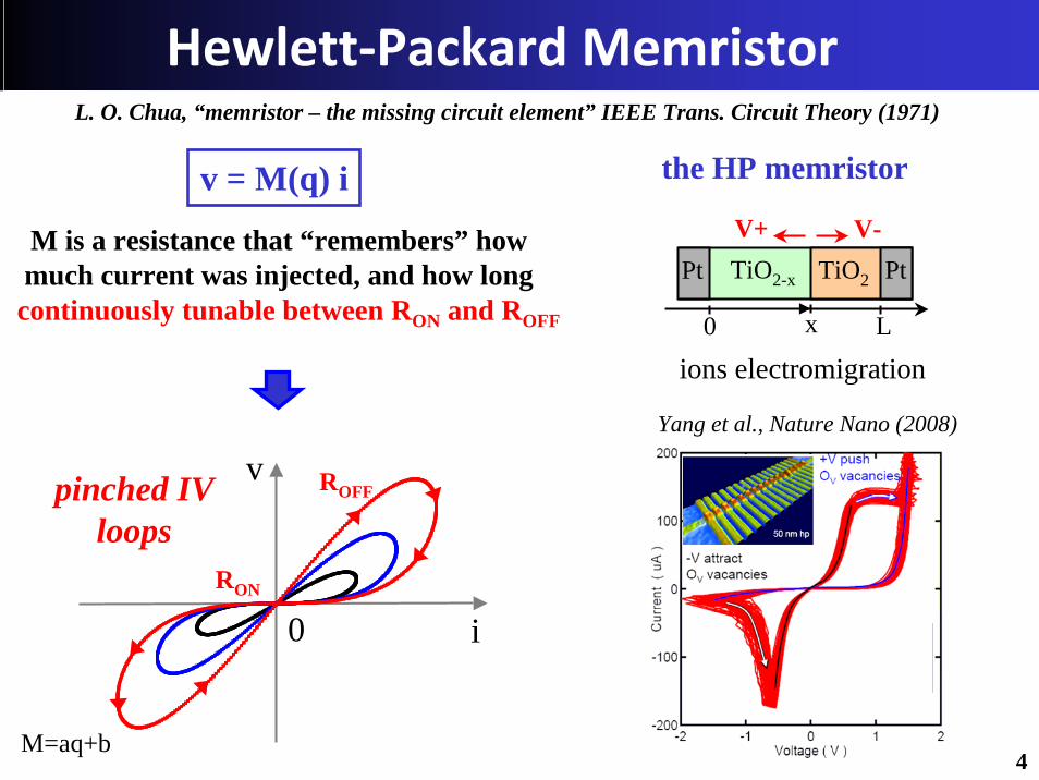
Hewlett‐Packard MemristorL. O. Chua, “memristor – the missing circuit element” IEEE Trans. Circuit Theory (1971)
v = M(q) i
pinched IV loops
M=aq+b
v
0
ROFF
RON
the HP memristor
0 x L
V-V+Pt PtTiO2TiO2-x
ions electromigration
Yang et al., Nature Nano (2008)
i
M is a resistance that “remembers” how much current was injected, and how longcontinuously tunable between RON and ROFF
4
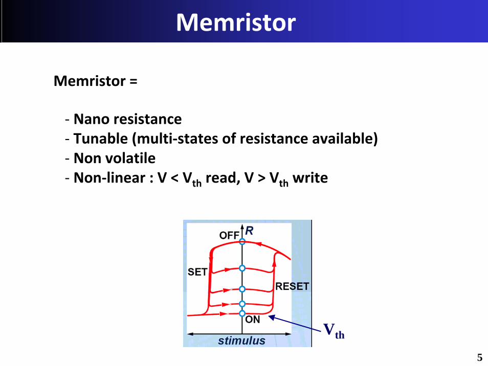
Memristor
Memristor =
‐ Nano resistance‐ Tunable (multi‐states of resistance available)‐ Non volatile‐ Non‐linear : V < Vth read, V > Vth write
Vth
5
Memristor technologies
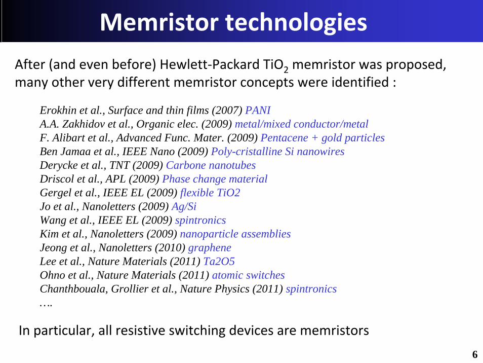
Erokhin et al., Surface and thin films (2007) PANIA.A. Zakhidov et al., Organic elec. (2009) metal/mixed conductor/metalF. Alibart et al., Advanced Func. Mater. (2009) Pentacene + gold particlesBen Jamaa et al., IEEE Nano (2009) Poly-cristalline Si nanowiresDerycke et al., TNT (2009) Carbone nanotubesDriscol et al., APL (2009) Phase change materialGergel et al., IEEE EL (2009) flexible TiO2Jo et al., Nanoletters (2009) Ag/SiWang et al., IEEE EL (2009) spintronicsKim et al., Nanoletters (2009) nanoparticle assembliesJeong et al., Nanoletters (2010) grapheneLee et al., Nature Materials (2011) Ta2O5Ohno et al., Nature Materials (2011) atomic switchesChanthbouala, Grollier et al., Nature Physics (2011) spintronics….
After (and even before) Hewlett‐Packard TiO2 memristor was proposed, many other very different memristor concepts were identified :
In particular, all resistive switching devices are memristors
6
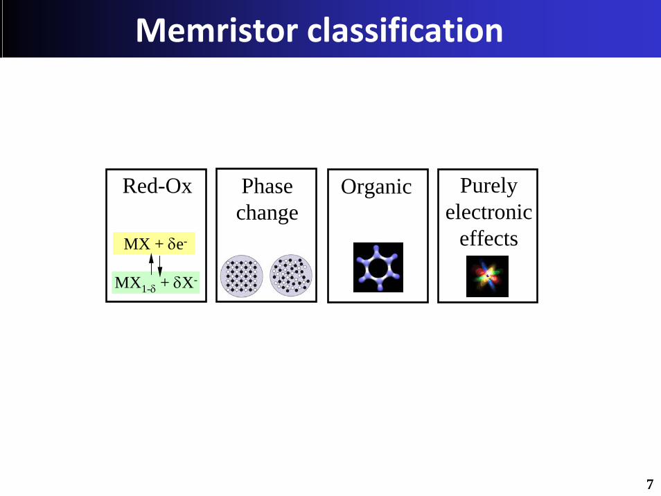
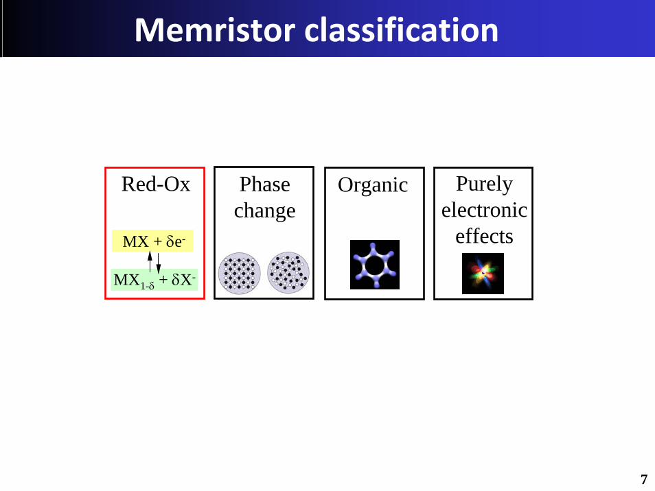
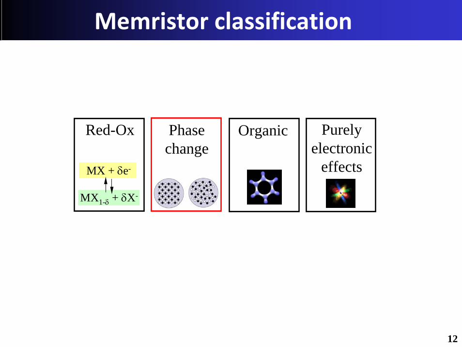
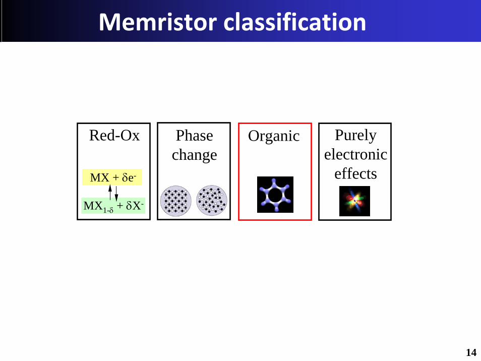
OrganicRed-Ox
MX + δe-
MX1-δ + δX-
Memristor classification
Phasechange
Purelyelectronic
effects
7
OrganicRed-Ox
MX + δe-
MX1-δ + δX-
Memristor classification
Phasechange
Purelyelectronic
effects
7
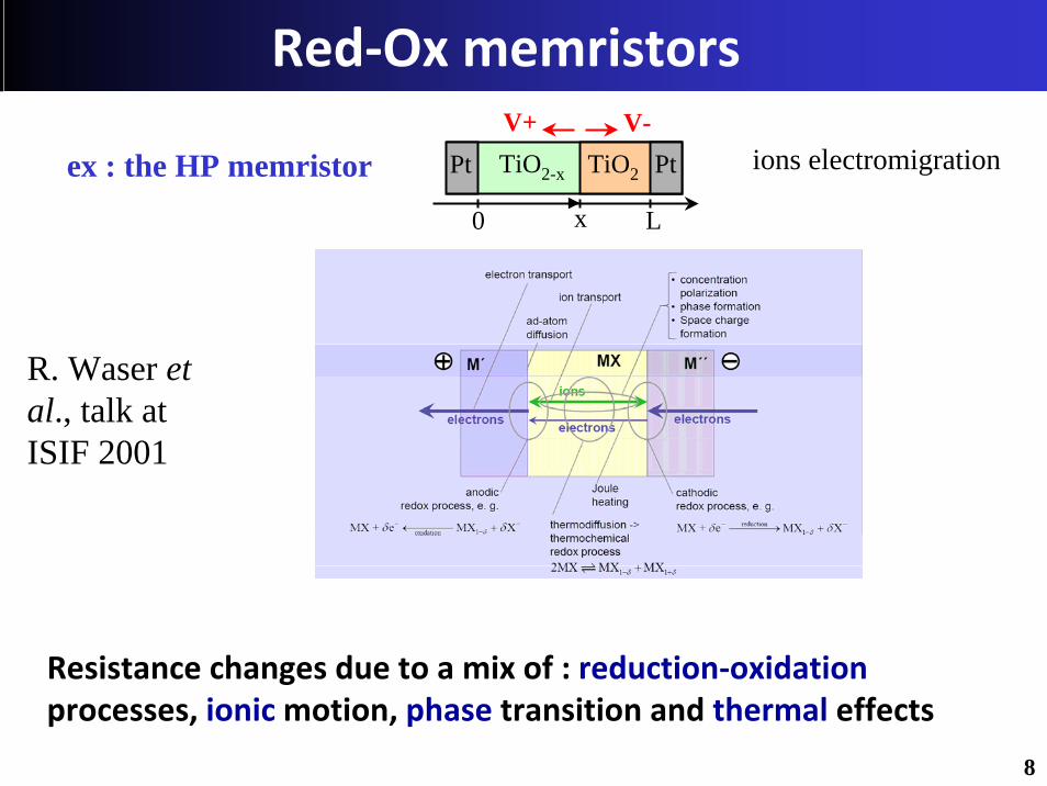
Red‐Ox memristors
ex : the HP memristor
0 x L
V-V+Pt PtTiO2TiO2-x ions electromigration
R. Waser et al., talk at ISIF 2001
Resistance changes due to a mix of : reduction‐oxidationprocesses, ionic motion, phase transition and thermal effects
8
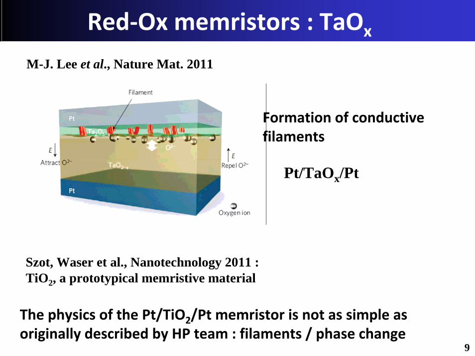
Red‐Ox memristors : TaOx
M-J. Lee et al., Nature Mat. 2011
Formation of conductive filaments
Pt/TaOx/Pt
Szot, Waser et al., Nanotechnology 2011 : TiO2, a prototypical memristive material
The physics of the Pt/TiO2/Pt memristor is not as simple as originally described by HP team : filaments / phase change
9
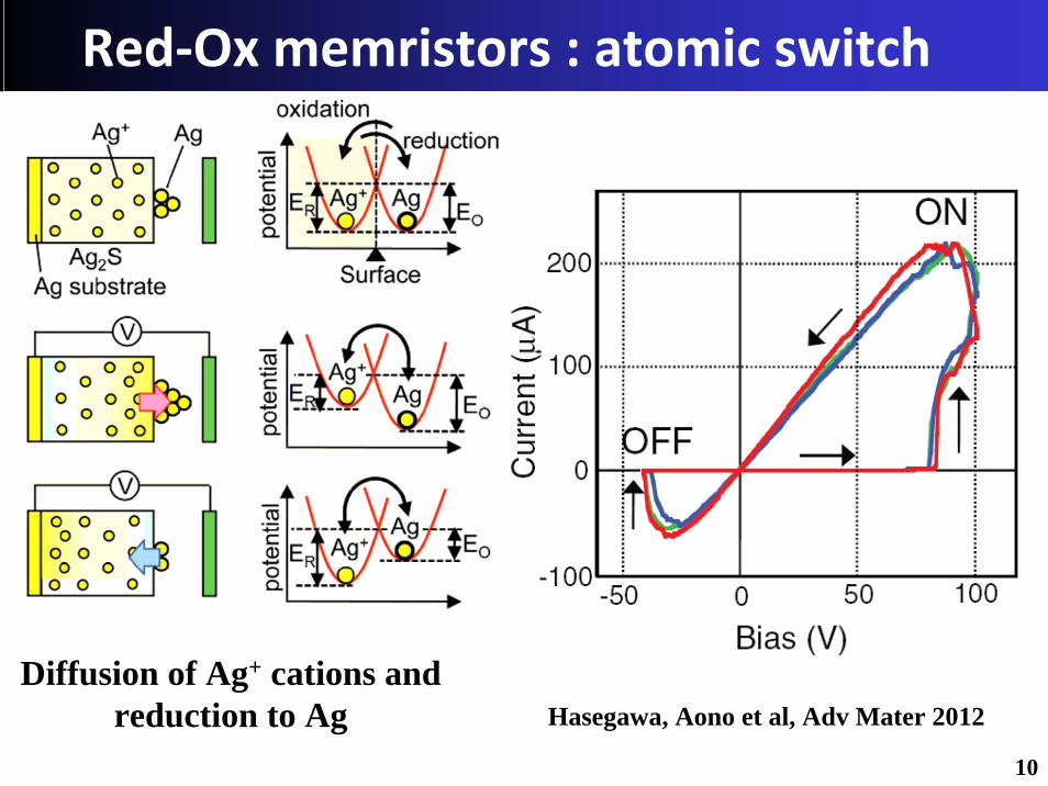
Red‐Ox memristors : atomic switch
Hasegawa, Aono et al, Adv Mater 2012Diffusion of Ag+ cations and
reduction to Ag 10
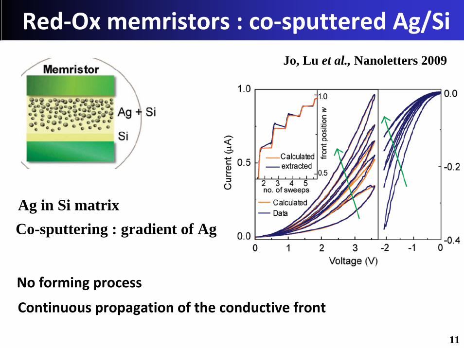
Red‐Ox memristors : co‐sputtered Ag/SiJo, Lu et al., Nanoletters 2009
Ag in Si matrixCo-sputtering : gradient of Ag
No forming process
Continuous propagation of the conductive front
11
OrganicRed-Ox
MX + δe-
MX1-δ + δX-
Memristor classification
Phasechange
Purelyelectronic
effects
12
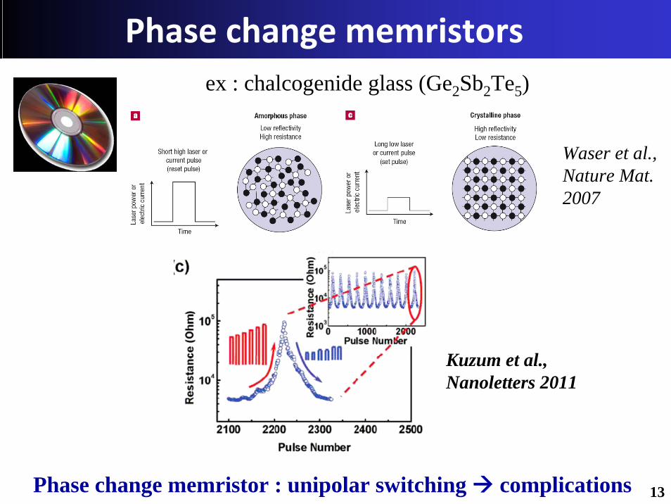
Phase change memristors
Kuzum et al., Nanoletters 2011
ex : chalcogenide glass (Ge2Sb2Te5)
Waser et al., Nature Mat. 2007
Phase change memristor : unipolar switching complications 13
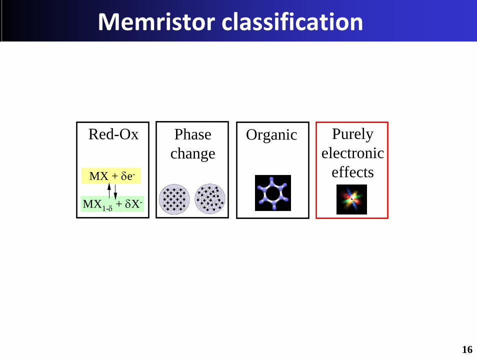
OrganicRed-Ox
MX + δe-
MX1-δ + δX-
Memristor classification
Phasechange
Purelyelectronic
effects
14
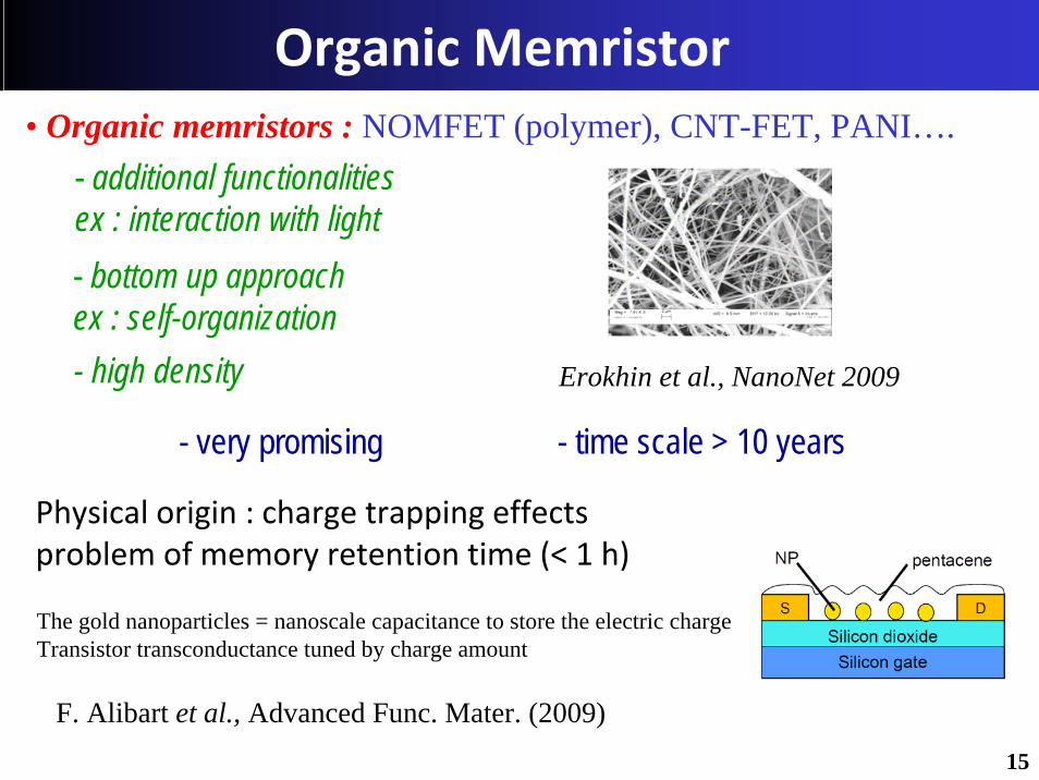
Organic Memristor • Organic memristors : NOMFET (polymer), CNT-FET, PANI….
- additional functionalities ex : interaction with light- bottom up approachex : self-organization
- very promising - time scale > 10 years
- high density Erokhin et al., NanoNet 2009
Physical origin : charge trapping effectsproblem of memory retention time (< 1 h)
F. Alibart et al., Advanced Func. Mater. (2009)
The gold nanoparticles = nanoscale capacitance to store the electric chargeTransistor transconductance tuned by charge amount
15
OrganicRed-Ox
MX + δe-
MX1-δ + δX-
Memristor classification
Phasechange
Purelyelectronic
effects
16
Phasechange
Red-Ox
MX + δe-
MX1-δ + δX-
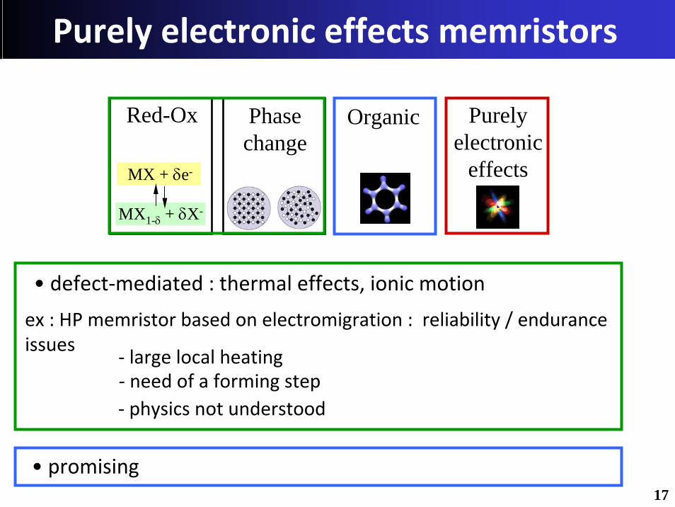
Purely electronic effects memristors
Purelyelectronic
effects
Organic
‐ large local heating
‐ physics not understood‐ need of a forming step
• defect‐mediated : thermal effects, ionic motion
ex : HP memristor based on electromigration : reliability / endurance issues
• promising17

Purely electronic effects memristors
obtain memristive effects by purely electronic physical mechanisms
Phasechange
Red-Ox
MX + δe-
MX1-δ + δX-
Purelyelectronic
effects
Organic
18

Spintronic memristor (MRAM based)
A. Chanthbouala, J. Grollier, R. Matsumoto, V. Cros, A. Anane, A. V. Khvalkovskiy, A. Fert
Unité Mixte de Physique CNRS/Thales, France
K.A. ZvezdinA.M. Prokhorov General Physics Institute of RAS, Russia
Istituto P.M. s.r.l., Italy
K. Nishimura, Y. Nagamine, H. Maehara, K. TsunekawaProcess Development Center, Canon ANELVA Corporation, Japan
A. Fukushima, and S. YuasaNational Institute of Advanced Industrial Science and Technology (AIST), Japan
Nanobrain 19
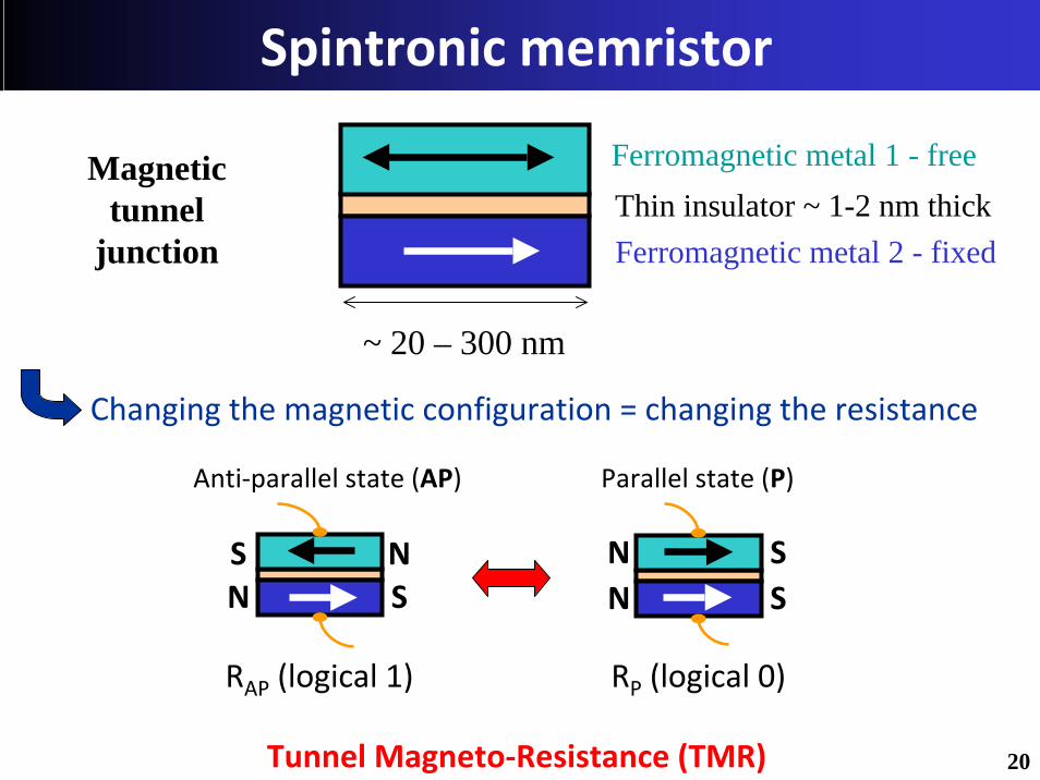
Spintronic memristor
Tunnel Magneto‐Resistance (TMR)
Changing the magnetic configuration = changing the resistance
Anti‐parallel state (AP)
RAP (logical 1)
NS N
S
Parallel state (P)
RP (logical 0)
NSNS
Ferromagnetic metal 1 - freeThin insulator ~ 1-2 nm thickFerromagnetic metal 2 - fixed
~ 20 – 300 nm
Magnetic tunnel
junction
20
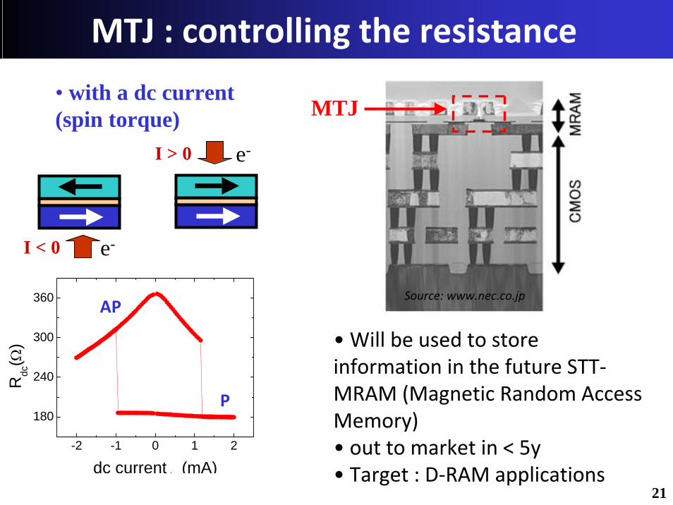
MTJ : controlling the resistance
-2 -1 0 1 2
180
240
300
360
Rdc
(Ω)
dc currentd (mA)
• with a dc current(spin torque)
e-I < 0
e-I > 0
AP
P
• Will be used to store information in the future STT‐MRAM (Magnetic Random Access Memory)• out to market in < 5y• Target : D‐RAM applications
Source: www.nec.co.jp
MTJ
21
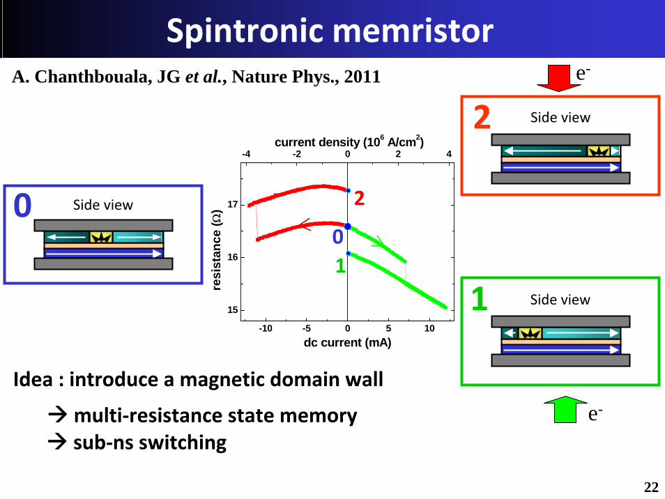
Spintronic memristor
-10 -5 0 5 10
15
16
17
-4 -2 0 2 4
resi
stan
ce (Ω
)
dc current (mA)
current density (106 A/cm2)
A. Chanthbouala, JG et al., Nature Phys., 2011
01
20 Side view
1 Side view
2 Side view
Idea : introduce a magnetic domain wall
multi‐resistance state memory
e-
e-
sub‐ns switching
22
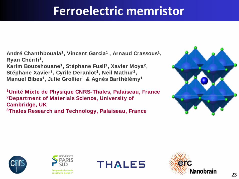
Ferroelectric memristor
André Chanthbouala1, Vincent Garcia1 , Arnaud Crassous1, Ryan Chérifi1, Karim Bouzehouane1, Stéphane Fusil1, Xavier Moya2, Stéphane Xavier3, Cyrile Deranlot1, Neil Mathur2, Manuel Bibes1, Julie Grollier1 & Agnès Barthélémy1
1Unité Mixte de Physique CNRS-Thales, Palaiseau, France2Department of Materials Science, University of Cambridge, UK3Thales Research and Technology, Palaiseau, France
Nanobrain 23

Ferroelectric memristor
P
E
Ferroelectrics
+
− +
−
Ferroelectric tunnel junctions
Garcia et al., Nature 460, 81 (2009)
Low R = RON Large R = ROFF
polarization
Switching of the polarization with an electric field
BaTiO3
24
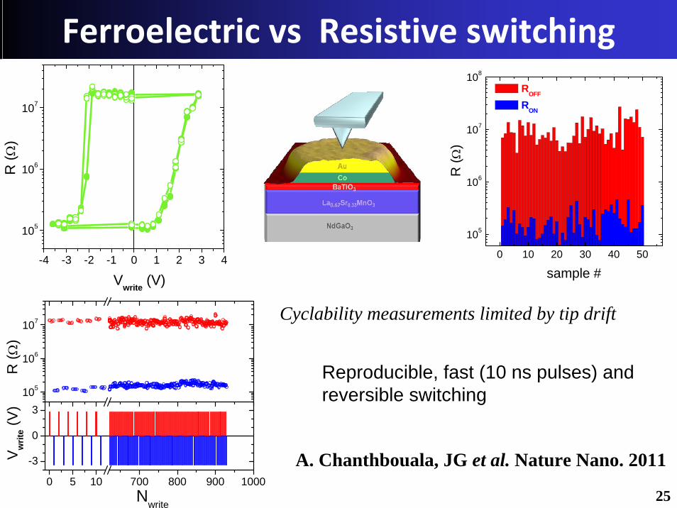
Ferroelectric vs Resistive switching
-4 -3 -2 -1 0 1 2 3 4
105
106
107
R (Ω
)
Vwrite (V)
0 10 20 30 40 50
105
106
107
108
R (Ω
)
sample #
ROFF
RON
105
106
107
0 5 10 700 800 900 1000
-3
0
3
R (Ω
)
Vw
rite (V
)
Nwrite
Cyclability measurements limited by tip drift
Reproducible, fast (10 ns pulses) and reversible switching
A. Chanthbouala, JG et al. Nature Nano. 2011
25
Outline
1- memristor devices : introduction
2- memristors as digital memory
3- memristors for logic applications
4- memristors for neuromorphic computing
26
Memristors as memory
Last 5 years : large improvements of memristor devices performance
switching speedendurance, reliability etc.
Hewlett-Packard annouced ReRAM out on the market in 2013 !
27
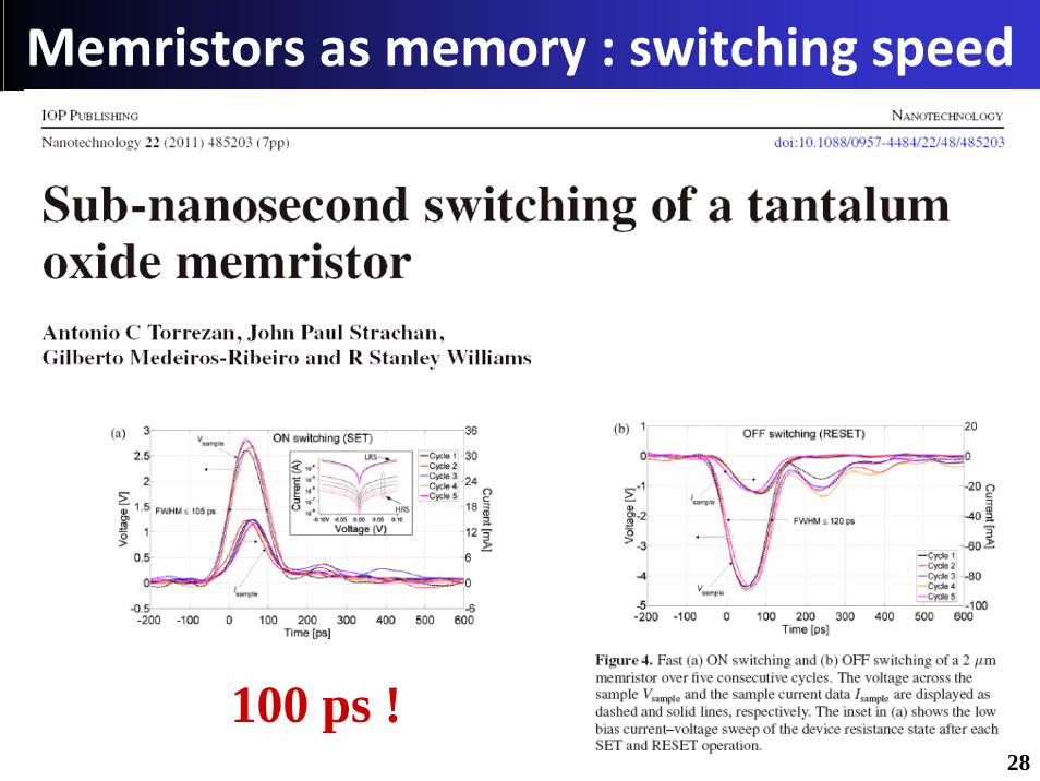
Memristors as memory : switching speed
100 ps !28
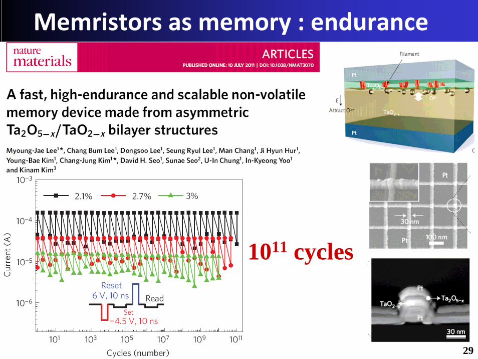
Memristors as memory : endurance
1011 cycles
29
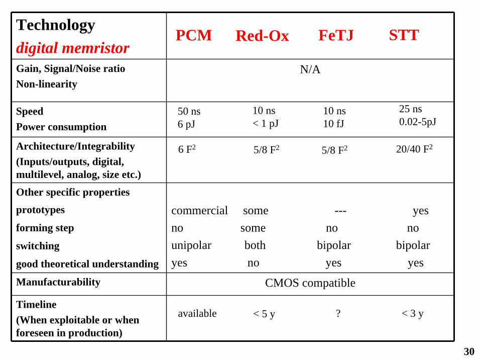
Technologydigital memristorGain, Signal/Noise ratioNon-linearity
N/A
SpeedPower consumption
Architecture/Integrability(Inputs/outputs, digital, multilevel, analog, size etc.)
Other specific properties
prototypes
forming step
switching
good theoretical understanding
commercial some --- yesno some no nounipolar both bipolar bipolaryes no yes yes
Manufacturability CMOS compatible
Timeline(When exploitable or when foreseen in production)
PCM Red-Ox FeTJ STT
25 ns0.02-5pJ
10 ns10 fJ
50 ns6 pJ
10 ns< 1 pJ
6 F2 5/8 F2 5/8 F2 20/40 F2
available < 5 y ? < 3 y
30
crossbar array (103 x 103 OFF/ON ratio 107)
• 1 memory element = 1 storage device – 1 selector
• High enough OFF/On ratio : possibility to remove the selector
or combine memristor type 1 : storage, memristor type 2 : selector
• Challenges for memory to replace Flash & SRAM:
Scale down below 15 nm+ low power, high speed, dense, non-volatile
31
Memristors as memory : arrays
•Memristor devices can be scaled down below 20 nm
filament, atomic switch intrisically small
limiting element : selector ?
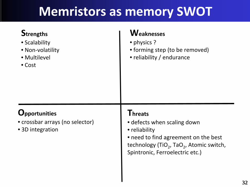
Memristors as memory SWOT
Strengths• Scalability• Non‐volatility• Multilevel• Cost
Weaknesses• physics ?• forming step (to be removed)• reliability / endurance
Threats• defects when scaling down• reliability• need to find agreement on the best technology (TiO2, TaO2, Atomic switch, Spintronic, Ferroelectric etc.)
32
Opportunities• crossbar arrays (no selector)• 3D integration
Outline
1- memristor devices : introduction
2- memristors as digital memory
3- memristors for logic applications
4- memristors for neuromorphic computing
33
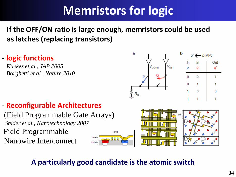
‐ logic functionsKuekes et al., JAP 2005Borghetti et al., Nature 2010
‐ Reconfigurable Architectures(Field Programmable Gate Arrays)Snider et al., Nanotechnology 2007 Field Programmable Nanowire Interconnect
Memristors for logicIf the OFF/ON ratio is large enough, memristors could be used as latches (replacing transistors)
A particularly good candidate is the atomic switch34
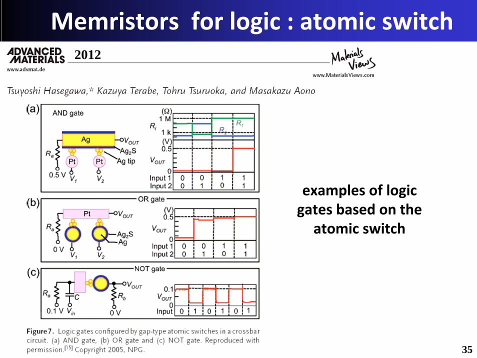
Memristors for logic : atomic switch2012
examples of logic gates based on the
atomic switch
35
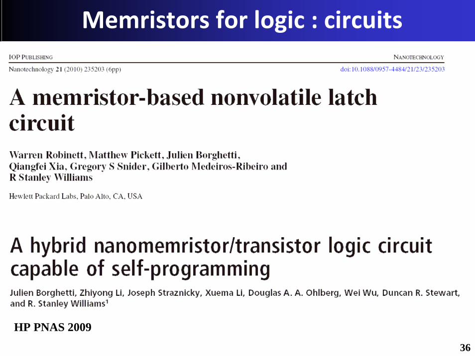
Memristors for logic : circuits
HP PNAS 2009
36
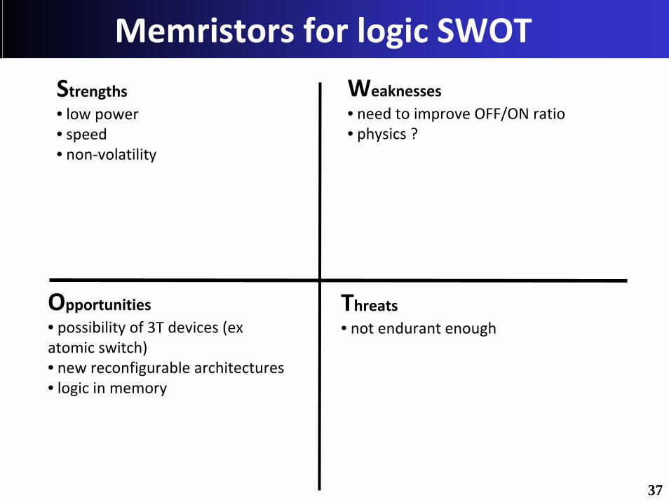
Memristors for logic SWOT
Strengths• low power• speed• non‐volatility
Weaknesses• need to improve OFF/ON ratio• physics ?
Threats• not endurant enough
Opportunities• possibility of 3T devices (ex atomic switch)• new reconfigurable architectures• logic in memory
37
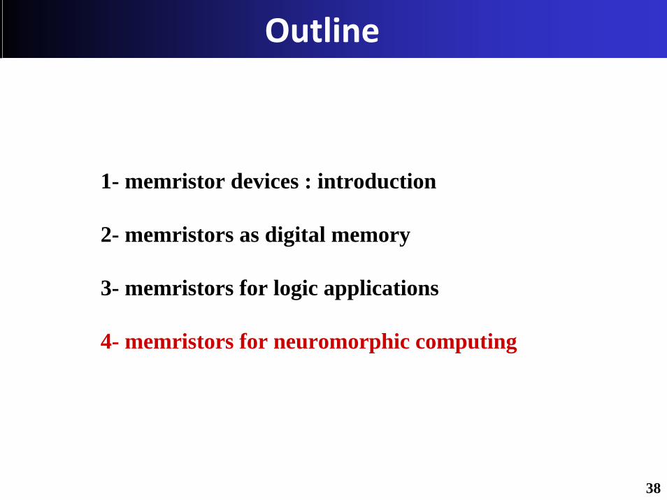
Outline
1- memristor devices : introduction
2- memristors as digital memory
3- memristors for logic applications
4- memristors for neuromorphic computing
38
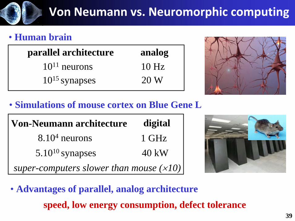
speed, low energy consumption, defect tolerance
8.104 neurons5.1010 synapses
1 GHz40 kW
digital
super-computers slower than mouse (×10)
1011 neurons1015 synapses
parallel architecture• Human brain
10 Hz20 W
• Advantages of parallel, analog architecture
• Simulations of mouse cortex on Blue Gene L
analog
Von-Neumann architecture
Von Neumann vs. Neuromorphic computing
39
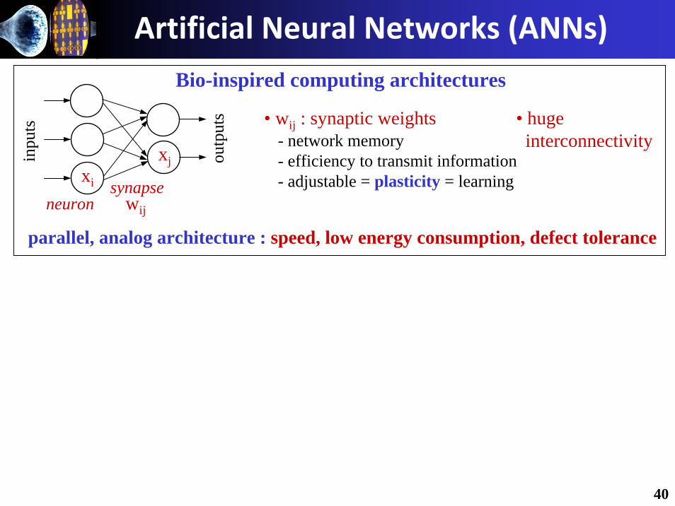
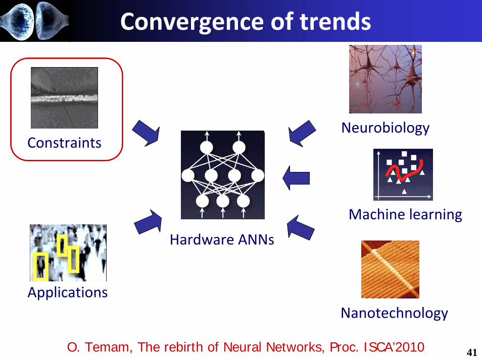
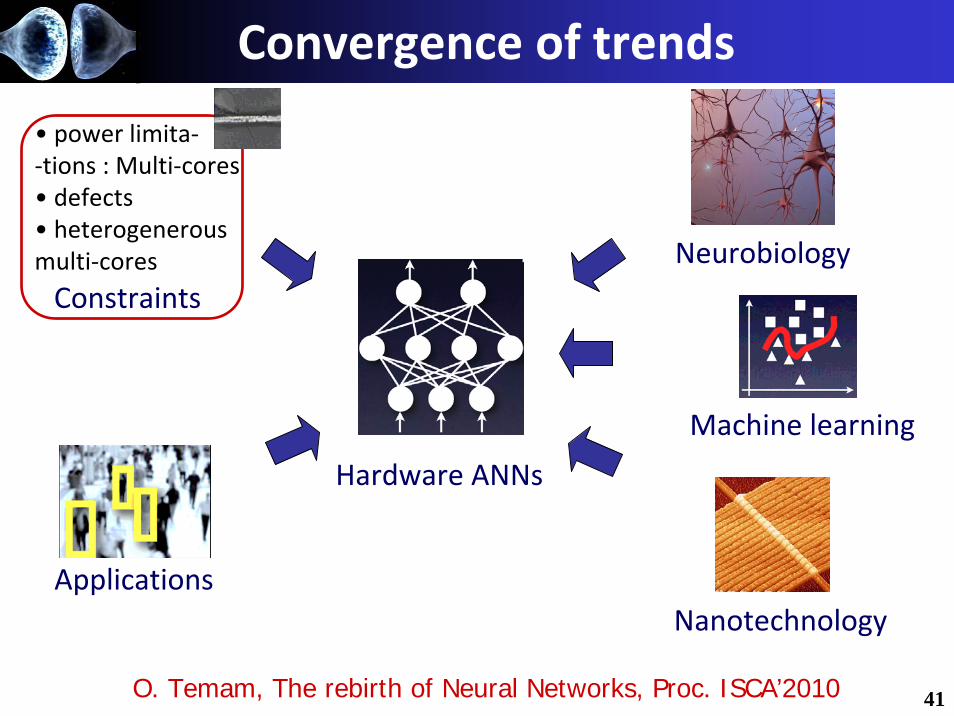
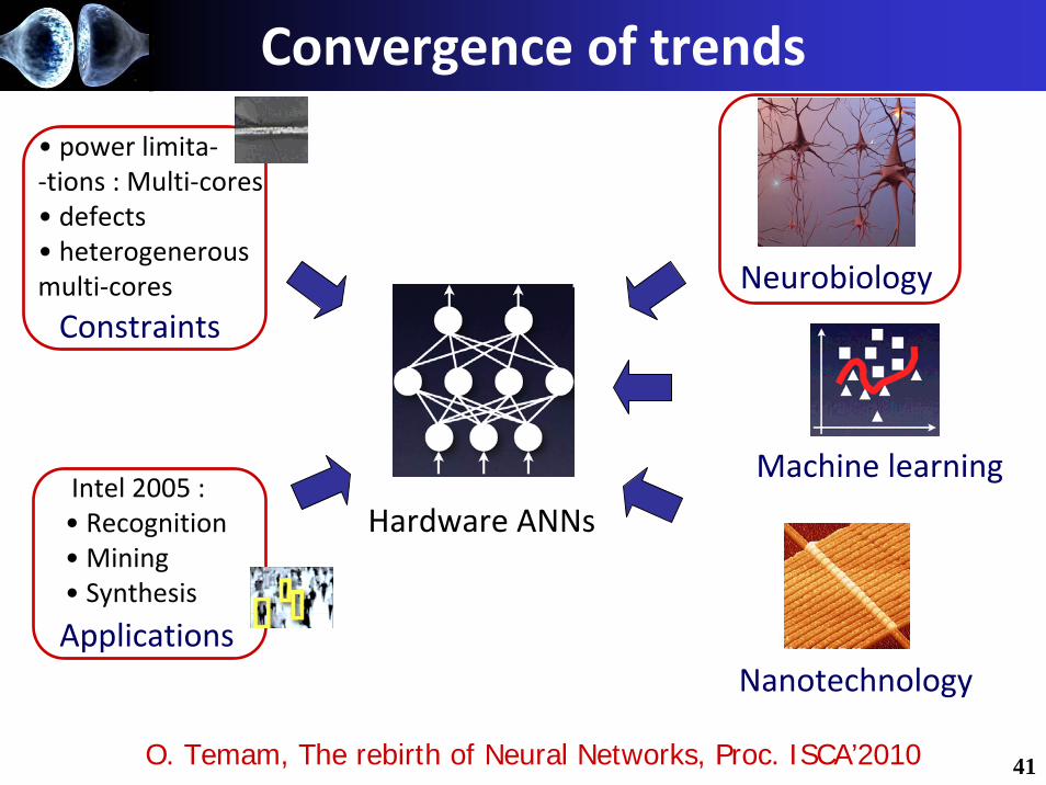
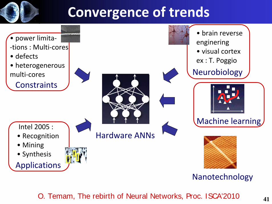
Artificial Neural Networks (ANNs)
wij
synapseneuron
inpu
ts
outp
uts
xjxi
• wij : synaptic weights - network memory- efficiency to transmit information- adjustable = plasticity = learning
• hugeinterconnectivity
Bio-inspired computing architectures
parallel, analog architecture : speed, low energy consumption, defect tolerance
40
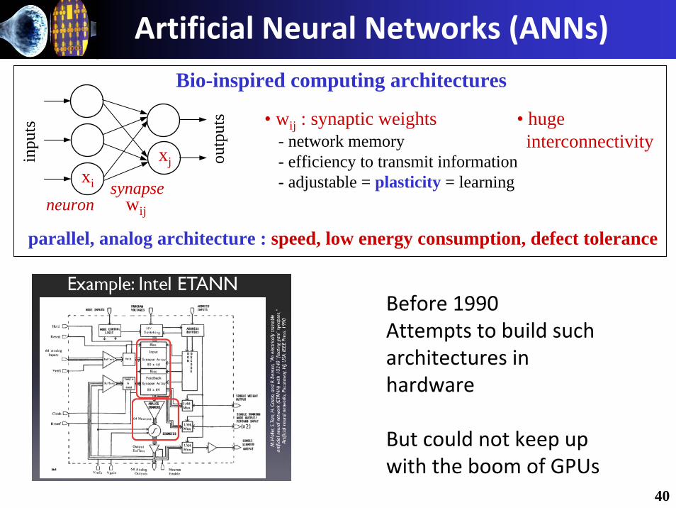
Artificial Neural Networks (ANNs)
Before 1990Attempts to build such architectures in hardware
But could not keep up with the boom of GPUs
wij
synapseneuron
inpu
ts
outp
uts
xjxi
• wij : synaptic weights - network memory- efficiency to transmit information- adjustable = plasticity = learning
• hugeinterconnectivity
Bio-inspired computing architectures
parallel, analog architecture : speed, low energy consumption, defect tolerance
40
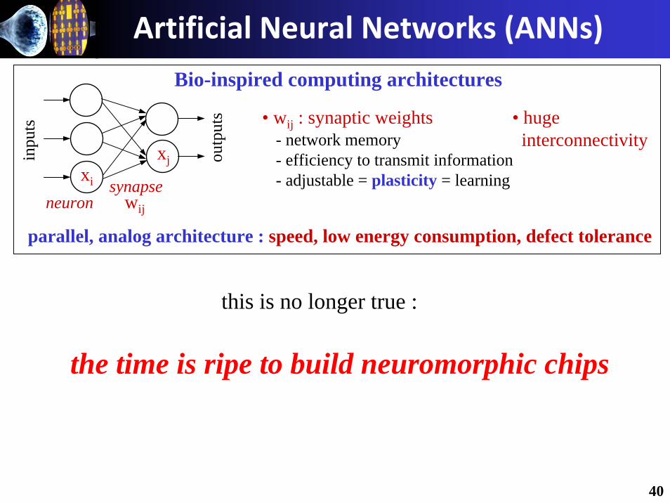
Artificial Neural Networks (ANNs)
the time is ripe to build neuromorphic chips
this is no longer true :
wij
synapseneuron
inpu
ts
outp
uts
xjxi
• wij : synaptic weights - network memory- efficiency to transmit information- adjustable = plasticity = learning
• hugeinterconnectivity
Bio-inspired computing architectures
parallel, analog architecture : speed, low energy consumption, defect tolerance
40
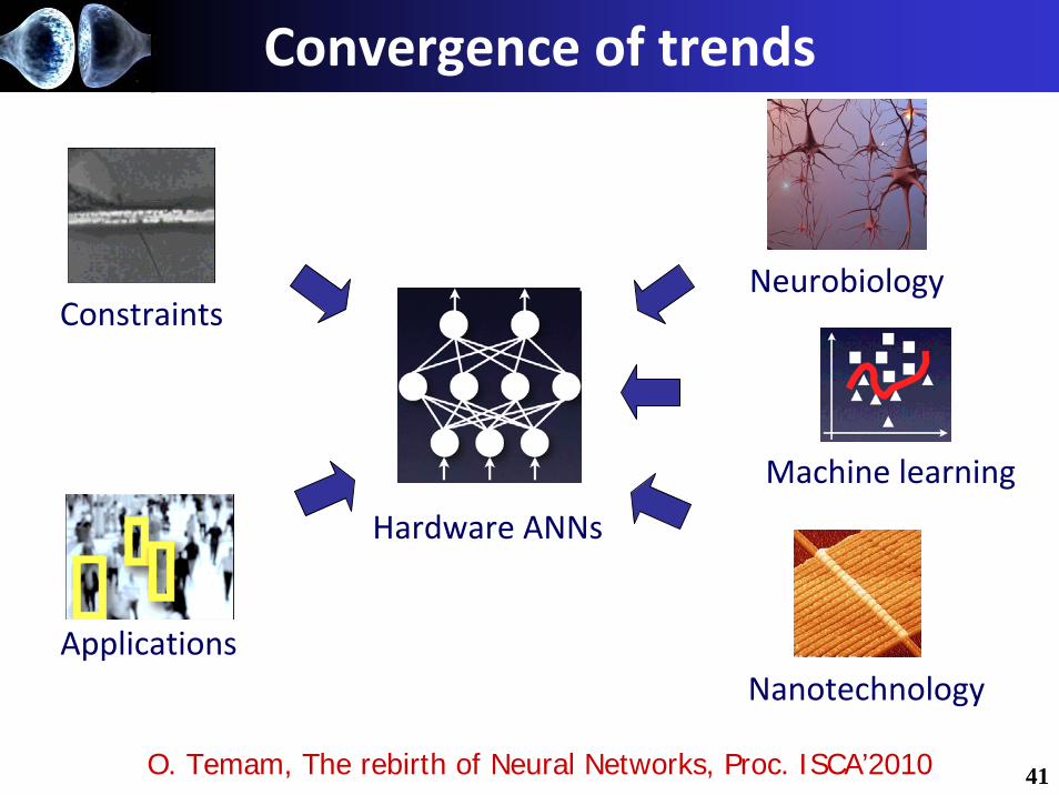
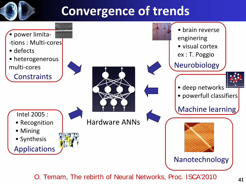
O. Temam, The rebirth of Neural Networks, Proc. ISCA’2010
Neurobiology
Machine learning
Hardware ANNs
Applications
Constraints
Nanotechnology
Convergence of trends
41
O. Temam, The rebirth of Neural Networks, Proc. ISCA’2010
Neurobiology
Machine learning
Hardware ANNs
Applications
Constraints
Nanotechnology
Convergence of trends
41
O. Temam, The rebirth of Neural Networks, Proc. ISCA’2010
Neurobiology
Machine learning
Hardware ANNs
Applications
Constraints
Nanotechnology
Convergence of trends
• power limita‐‐tions : Multi‐cores• defects• heterogenerous multi‐cores
41

O. Temam, The rebirth of Neural Networks, Proc. ISCA’2010
Neurobiology
Machine learning
Hardware ANNs
Applications
Constraints
Nanotechnology
Convergence of trends
• power limita‐‐tions : Multi‐cores• defects• heterogenerous multi‐cores
41

O. Temam, The rebirth of Neural Networks, Proc. ISCA’2010
Neurobiology
Machine learning
Hardware ANNs
Applications
Constraints
Nanotechnology
Convergence of trends
• power limita‐‐tions : Multi‐cores• defects• heterogenerous multi‐cores
Intel 2005 :• Recognition• Mining • Synthesis
41
O. Temam, The rebirth of Neural Networks, Proc. ISCA’2010
Neurobiology
Applications
Constraints
Machine learning
Hardware ANNs
Nanotechnology
Convergence of trends
• power limita‐‐tions : Multi‐cores• defects• heterogenerous multi‐cores
Intel 2005 :• Recognition• Mining • Synthesis
41

O. Temam, The rebirth of Neural Networks, Proc. ISCA’2010
Neurobiology
Applications
Constraints
Machine learning
Hardware ANNs
Nanotechnology
Convergence of trends
• power limita‐‐tions : Multi‐cores• defects• heterogenerous multi‐cores
Intel 2005 :• Recognition• Mining • Synthesis
• brain reverse enginering• visual cortexex : T. Poggio
41
O. Temam, The rebirth of Neural Networks, Proc. ISCA’2010
Neurobiology
Machine learning
Applications
Constraints
Hardware ANNs
Nanotechnology
Convergence of trends
• power limita‐‐tions : Multi‐cores• defects• heterogenerous multi‐cores
Intel 2005 :• Recognition• Mining • Synthesis
• brain reverse enginering• visual cortexex : T. Poggio
41

O. Temam, The rebirth of Neural Networks, Proc. ISCA’2010
Neurobiology
Machine learning
Applications
Constraints
Hardware ANNs
Nanotechnology
Convergence of trends
• power limita‐‐tions : Multi‐cores• defects• heterogenerous multi‐cores
Intel 2005 :• Recognition• Mining • Synthesis
• brain reverse enginering• visual cortexex : T. Poggio
• deep networks• powerfull classifiers
41
O. Temam, The rebirth of Neural Networks, Proc. ISCA’2010
Neurobiology
Machine learning
Applications
Constraints
Nanotechnology
Hardware ANNs
Convergence of trends
• power limita‐‐tions : Multi‐cores• defects• heterogenerous multi‐cores
Intel 2005 :• Recognition• Mining • Synthesis
• brain reverse enginering• visual cortexex : T. Poggio
• deep networks• powerfull classifiers
• 1 memristor = 1 synapse
• 3D stacking• 104 synapses/neuron
41
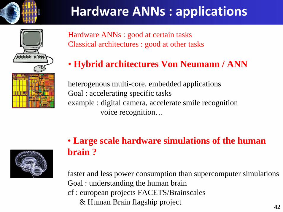
Hardware ANNs : good at certain tasksClassical architectures : good at other tasks
• Hybrid architectures Von Neumann / ANN
heterogenous multi-core, embedded applicationsGoal : accelerating specific tasksexample : digital camera, accelerate smile recognition
voice recognition…
Hardware ANNs : applications
• Large scale hardware simulations of the human brain ?
faster and less power consumption than supercomputer simulationsGoal : understanding the human brain cf : european projects FACETS/Brainscales
& Human Brain flagship project 42
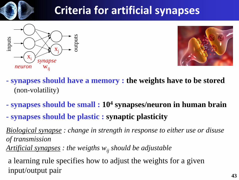
wij
synapseneuron
inpu
ts
outp
uts
xjxi
Biological synapse
- synapses should be plastic : synaptic plasticity
: change in strength in response to either use or disuse of transmissionArtificial synapses : the weigths wij should be adjustable
Criteria for artificial synapses
a learning rule specifies how to adjust the weights for a giveninput/output pair
- synapses should be small : 104 synapses/neuron in human brain
(non-volatility)
43
- synapses should have a memory : the weights have to be stored
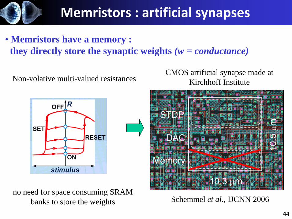
Memristors : artificial synapses
FACETS chip
• Memristors have a memory : they directly store the synaptic weights (w = conductance)
Non-volative multi-valued resistances CMOS artificial synapse made at
Kirchhoff Institute
Schemmel et al., IJCNN 2006no need for space consuming SRAM
banks to store the weights44
Memristors : artificial synapses
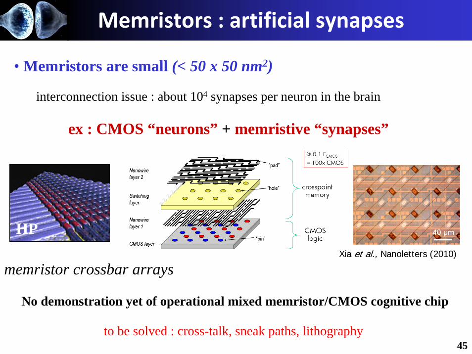
• Memristors are small (< 50 x 50 nm2)
interconnection issue : about 104 synapses per neuron in the brain
ex : CMOS “neurons” + memristive “synapses”
Xia et al., Nanoletters (2010)
HP
memristor crossbar arrays
to be solved : cross-talk, sneak paths, lithography
No demonstration yet of operational mixed memristor/CMOS cognitive chip
45
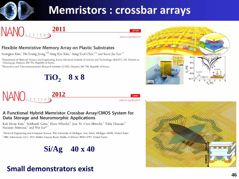
8 x 8
40 x 40
2012
Si/Ag
TiO2
2011
46
Memristors : crossbar arrays
Small demonstrators exist
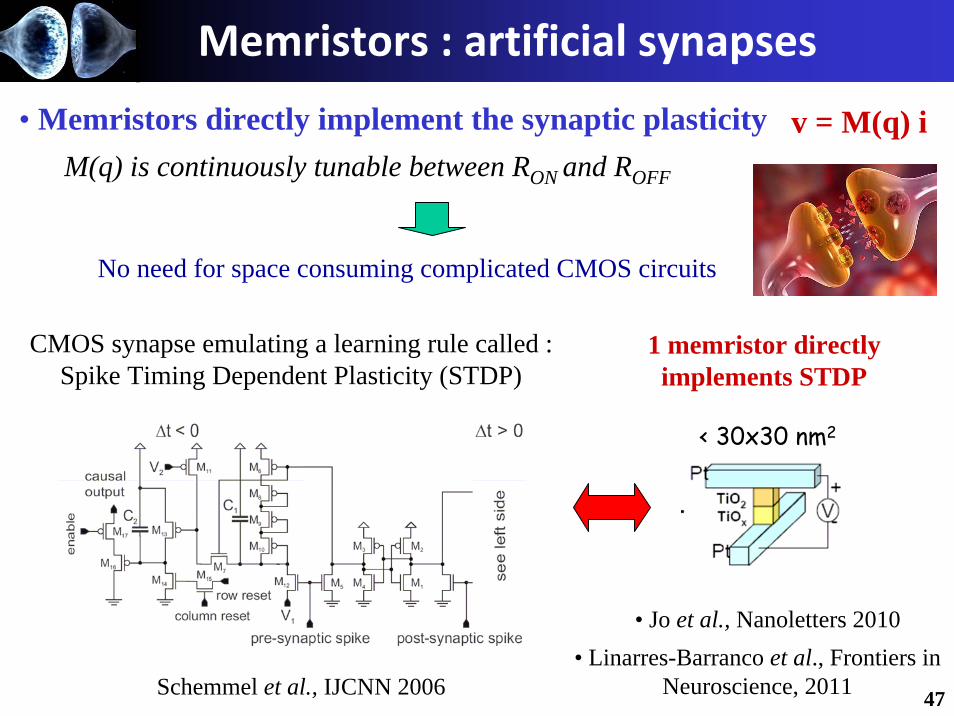
• Memristors directly implement the synaptic plasticity v = M(q) i
Memristors : artificial synapses
M(q) is continuously tunable between RON and ROFF
No need for space consuming complicated CMOS circuits
Schemmel et al., IJCNN 2006
CMOS synapse emulating a learning rule called :Spike Timing Dependent Plasticity (STDP)
< 30x30 nm2
• Linarres-Barranco et al., Frontiers in Neuroscience, 2011
1 memristor directly implements STDP
• Jo et al., Nanoletters 2010
47
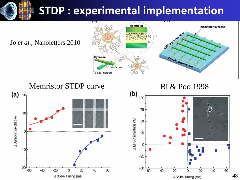
STDP : experimental implementation
Bi & Poo 1998Memristor STDP curve
48
Jo et al., Nanoletters 2010
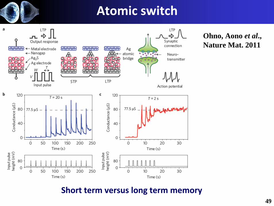
Atomic switch
Ohno, Aono et al., Nature Mat. 2011
49
Short term versus long term memory
neuromorphic architectures
interconnect
programming
• common points
• common challenges
communication with classical computing architectures50
• different levels of abstraction
at the cell level (neuron)
at the molecular level (biochemival reaction)
• inspiration from biology and cell signalling process
massively paralleltake advantage of the noise (stochasticity)
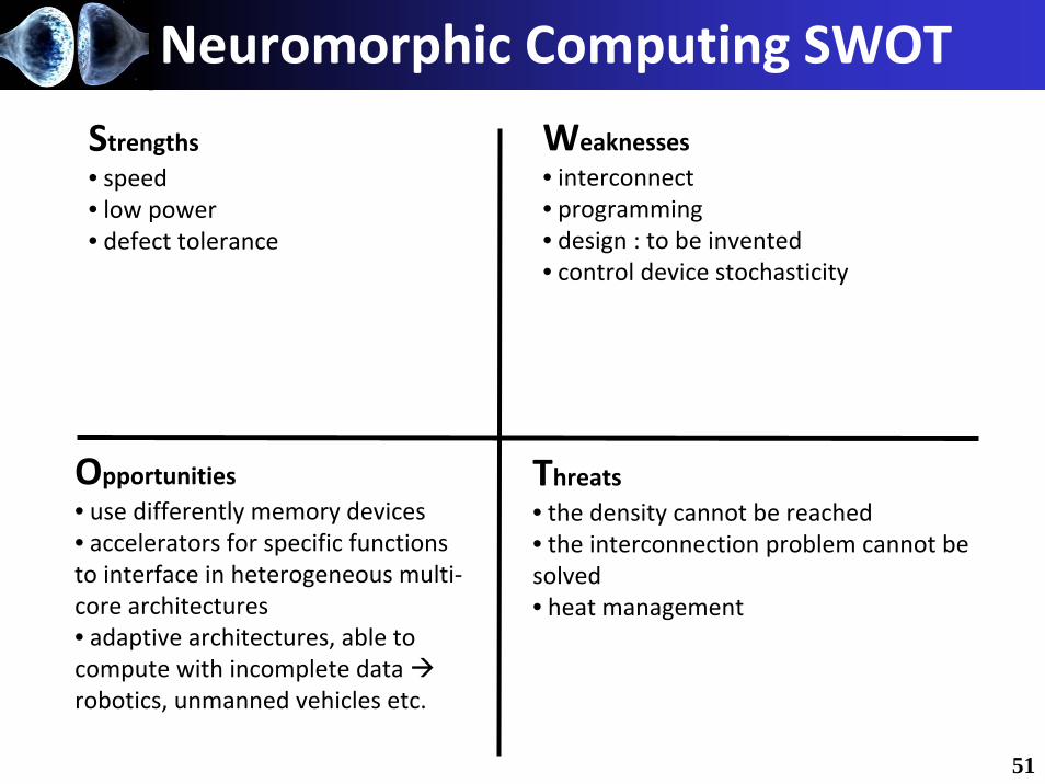
Neuromorphic Computing SWOT
Strengths• speed• low power• defect tolerance
Weaknesses• interconnect• programming• design : to be invented• control device stochasticity
Opportunities• use differently memory devices• accelerators for specific functions to interface in heterogeneous multi‐core architectures• adaptive architectures, able to compute with incomplete data robotics, unmanned vehicles etc.
Threats• the density cannot be reached• the interconnection problem cannot be solved• heat management
51
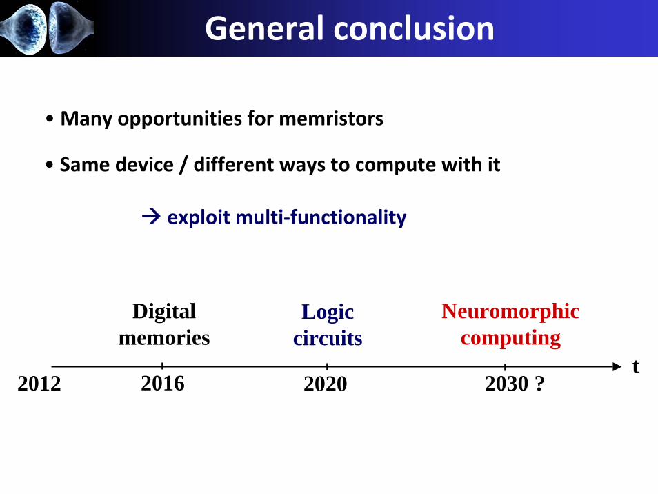
General conclusion
•Many opportunities for memristors
Digital memories
Logic circuits
Neuromorphic computing
• Same device / different ways to compute with it
t2012 2016 2020 2030 ?
exploit multi‐functionality

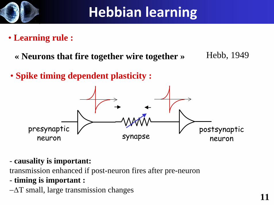
Hebbian learning
« Neurons that fire together wire together » Hebb, 1949
• Learning rule :
• Spike timing dependent plasticity :
presynapticneuron
postsynaptic neuronsynapse
- causality is important:transmission enhanced if post-neuron fires after pre-neuron- timing is important :−ΔT small, large transmission changes
11
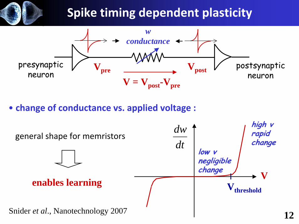
Spike timing dependent plasticity
enables learning
• change of conductance vs. applied voltage :
V
low vnegligiblechange
high vrapid changedt
dw
Vthreshold
presynapticneuron
postsynaptic neuron
Vpre
wconductance
Vpost
V = Vpost-Vpre
general shape for memristors
Snider et al., Nanotechnology 2007 12
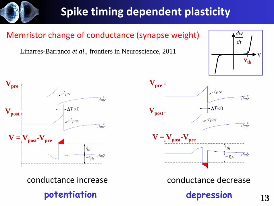
Spike timing dependent plasticity
v
dtdw
vth
Memristor change of conductance (synapse weight)
Linarres-Barranco et al., frontiers in Neuroscience, 2011
conductance increase conductance decrease
potentiation depression
Vpre
Vpost
V = Vpost-Vpre
Vpre
Vpost
V = Vpost-Vpre
13
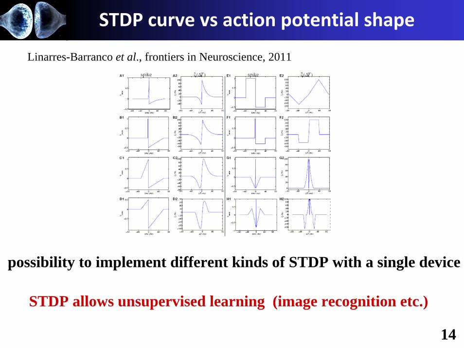
STDP curve vs action potential shape
Linarres-Barranco et al., frontiers in Neuroscience, 2011
possibility to implement different kinds of STDP with a single device
14
STDP allows unsupervised learning (image recognition etc.)
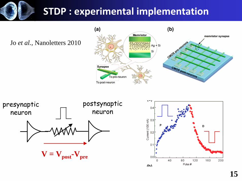
STDP : experimental implementation
Jo et al., Nanoletters 2010
presynapticneuron
postsynaptic neuron
V = Vpost-Vpre
15
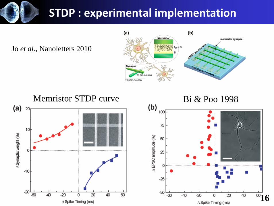
STDP : experimental implementation
Bi & Poo 1998
16
Jo et al., Nanoletters 2010
Memristor STDP curve
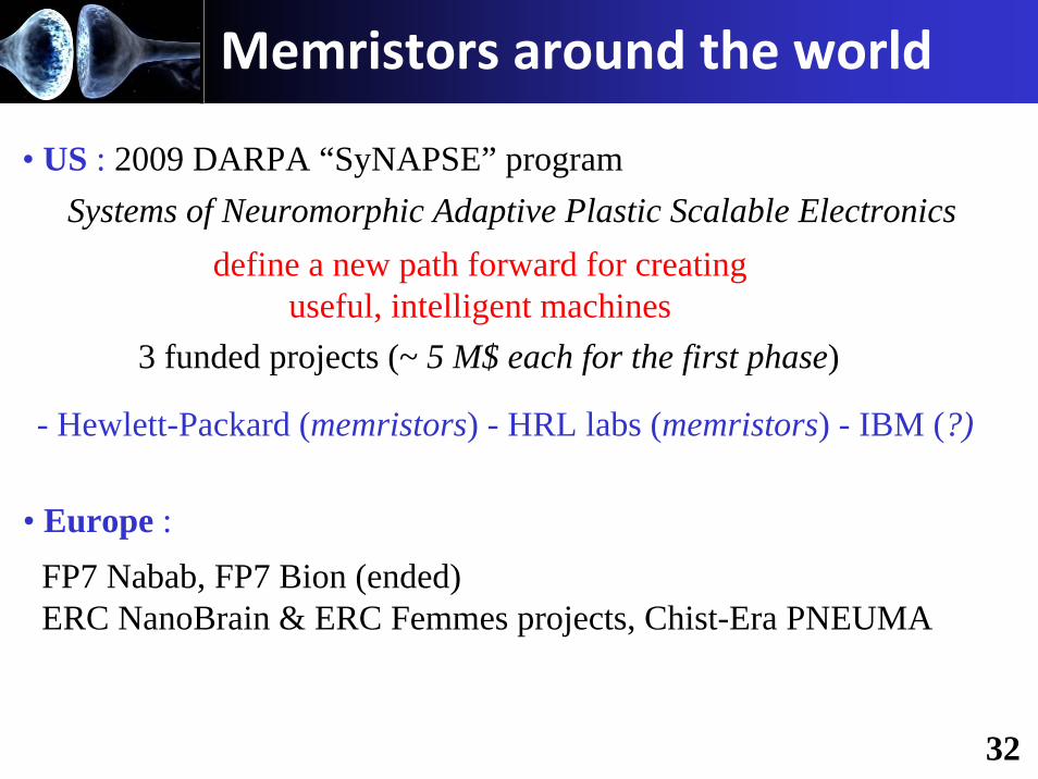
• US : 2009 DARPA “SyNAPSE” program
- Hewlett-Packard (memristors) - HRL labs (memristors) - IBM (?)
define a new path forward for creating useful, intelligent machines
Memristors around the world
3 funded projects (~ 5 M$ each for the first phase)
Systems of Neuromorphic Adaptive Plastic Scalable Electronics
• Europe : FP7 Nabab, FP7 Bion (ended)ERC NanoBrain & ERC Femmes projects, Chist-Era PNEUMA
32
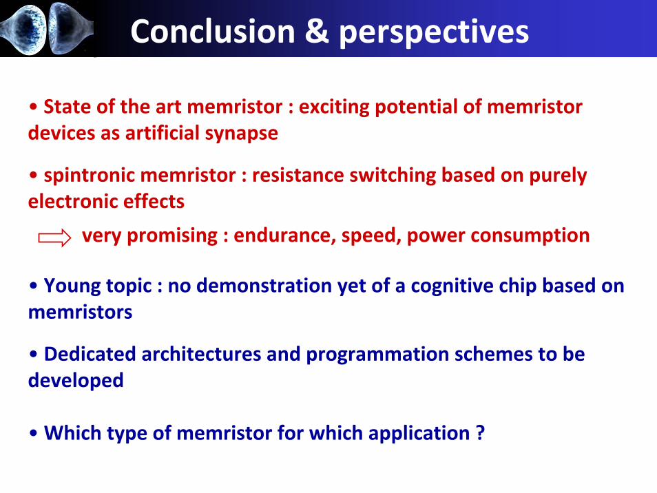
Conclusion & perspectives
• State of the art memristor : exciting potential of memristor devices as artificial synapse
• spintronic memristor : resistance switching based on purely electronic effects
very promising : endurance, speed, power consumption
• Young topic : no demonstration yet of a cognitive chip based on memristors
• Dedicated architectures and programmation schemes to be developed
•Which type of memristor for which application ?

Acknowledgements
Funding :
‐ ERC Starting Grant 259068 Nanobrain
‐ ANR P2N MHANN « Memristive Hardware Artificial neural Networks Accelerators »
‐ PEPS project ACME « Memristive Accelerators »
R. Waser, ISIF 2011