Embed Size (px)
Citation preview
Turk J Elec Eng & Comp Sci
(2014) 22: 573 – 581
c⃝ TUBITAK
doi:10.3906/elk-1207-106
Turkish Journal of Electrical Engineering & Computer Sciences
http :// journa l s . tub i tak .gov . t r/e lektr ik/
Research Article
Neuro-fuzzy network approach for modeling submicron MOSFETs: application to
MOSFET subcircuit simulation
Amir Hossein ABDOLLAHI NOHOJI1,∗, Fardad FAROKHI2, Majid ZAMANI31Young Researchers and Elite Club, Central Tehran Branch, Islamic Azad University, Tehran, Iran
2Department of Electrical Engineering, Central Tehran Branch, Islamic Azad University, Tehran, Iran3Department of Electrical Engineering, Science and Research Branch, Islamic Azad University, Tehran, Iran
Received: 26.07.2012 • Accepted: 11.12.2012 • Published Online: 21.03.2014 • Printed: 18.04.2014
Abstract: A neuro-fuzzy network approach is developed to model the nonlinear behavior of submicron metal-oxide
semiconductor field-effect transistors (MOSFETs). The proposed model is trained and implemented as a MOSFET in a
software environment. The training data are obtained through various simulations of a MOSFET Berkeley short channel
insulated-gate field-effect transistor model 3 (BSIM3) in HSPICE, and the trained model is utilized to simulate the
MOSFET device. The obtained result shows good and noticeable agreement between the numerical result of the original
model in HSPICE and the neuro-fuzzy approach in the device and subcircuit modeling.
Key words: Neuro-fuzzy networks, MOSFET subcircuit implementation, HSPICE
1. Introduction
With rapid changes in metal oxide semiconductor (MOS) transistors [1,2] in manufacturing technology, many
new models are implemented and introduced to simulate the new MOS field-effect transistor’s (MOSFET’s)
behavior, faster and more accurately, so that the modeling process serves an important role in the design cycle.
Therefore, it is essential for computer-aided design simulators to have a reliable model approach and
effective parameters to characterize the device’s nonlinear behavior.
MOSFET device models based on equivalent circuits are developed based on lumped element formulas,
whereas equivalent circuit approaches require more experience and they are very complicated.
Today, the Berkeley short channel insulated-gate field-effect transistor model (BSIM) has become an
industrial standard model for simulating MOSFET transistors [3]. Each model consists of several parameters
to be simulated in the simulator program in HSPICE.
Recently, artificial neural networks (ANNs) were introduced as a powerful tool for optimization and
modeling electronic devices and circuits [4,5]. ANNs can be developed even if the equivalent circuit and
equation of the device are unavailable [6]. In [6], for instance, training was done using only Vds and Vgs
for the modeling of a MOSFET DC current using a well-known multilayer perceptron (MLP) network with 15
hidden neurons and the mean squared error (MSE) of 2.3e–4 was achieved. However, other effective parameters
of the MOSFET model were neglected and those parameters dramatically decreased the network accuracy in
submicron simulations.
∗Correspondence: [email protected]
573
ABDOLLAHI NOHOJI et al./Turk J Elec Eng & Comp Sci
In [7], a MOSFET was modeled by L, tox, tsi, Vds , and Vgs using a MLP neural network (NN) with 2
hidden layers, and an output error of less than 5% was obtained, but it could have been more accurate in drain
current modeling.
In [8], the presented approach contained the analytical modeling of a dual-gate MOSFET using a neuro-
fuzzy network (NFN) and the model capabilities were proven for electron density, subband energy, and Id vs.
Vds determination, but the authors did not use their implemented model for circuit analysis and it is not clear
whether the overall accuracy would be the same in a circuit analysis based on the model.
In this work, a BSIM3 MOSFET model with a Taiwan Semiconductor Manufacturing Company 0.18-µm
technology for W, and L 0.27 µm and 0.18 µm, is developed on a powerful NFN for MOSFET drain current
simulation.
The advantage of this work is to use the useful combination of the ANN structure for learning and flexible
mathematic capability (fuzzy logic), for the nonlinear behavior modeling of MOSFET devices, while keeping
the high accuracy of the model, and the implemented model is also used in the sample multidevice circuits in
HSPICE. Training data are obtained in HSPICE with the nominal parameters of the BSIM3 and the saved
data are imported into the MATLAB environment in order to train the NFN. The developed and tested NFN is
implemented in HSPICE [9] for device and circuit analysis. The used NFN is constructed as a fuzzy system with
a product inference engine, singleton fuzzifier, center average defuzzifier, and Gaussian membership functions.
The network has a fixed number of neurons (rules) and their parameters are tuned during the training phase.
2. Neuro-fuzzy architecture
When using MOSFET modeling as a black box, nonlinear complex equations of the device are not required
and MOSFET numerical parameter extraction can be omitted in difficult and time consuming situations [10].
The ANN structure consists of neurons, which contain an input, weight coefficient, and a nonlinear activation
function. The network is organized as input, output, and hidden layers [11].
The training process consists of running the program several times in order to minimize the MSE for the
known output instances.
In this work, a neuro-fuzzy classifier is chosen with singleton fuzzifier, center average defuzzifier, and
Gaussian membership functions. The whole fuzzy system can be represented as the following equation:
f(out)=
M∑l=1
wl
n∏i=1
exp
(−(
ini−tfi
sigi
)2)M∑l=1
n∏i=1
exp
(−(
ini−tfi
sigi
)2) , (1)
where in i are input data, n is the number of training features, M is the number of fuzzy rules (neurons), and
tf , sig , and w are free parameters for the NFN training and should be optimized during the training phase
using the gradient descent method [12].
The training phase has the following stages:
Stage 1. The input data (ini) are passed through a Gaussian operator, as Eq. (2).
GMF (i)=exp
(−(ini−tf i
sigi
)2)
(2)
574
ABDOLLAHI NOHOJI et al./Turk J Elec Eng & Comp Sci
Stage 2. The results of stage 1 for all of the individual inputs are calculated and multiplied by each other.
z=n∏
i=1
exp
(−(ini−tf i
sigi
)2)
(3)
Stage 3. The center average defuzzification is evaluated to determine the developed output Z with the M fuzzy
rule, as Eq. (4).
f(out)=
M∑l=1
wlzl
M∑l=1
zl
=b
a(4)
It is assumed that:
b =M∑l=1
wlzl, a =M∑l=1
zl. (5, 6)
The free parameters should be updated using the gradient descent algorithm, as follows [12]:
Error=e=1
2
[f(out)−y(out)
]2, (7)
and
w(q+1) = w(q) − α∂e
∂w, (8)
∂e
∂w=(f(out)−y(out)
) ∂f(out)∂a
∂a
∂w. (9)
By substituting Eq. (9) into Eq. (8), Eq. (10) is obtained:
w(q+1)=w(q)−α
(f(out)−y(out)
b
)z, (10)
where α is the learning rate and is considered to be less than 1; f(out) is the estimated output, while y(out)
shows the desired output, which is given by the supervisor.
tf and sig are obtained as well (see Eqs. (11)–(15)):
tf (q+1) = tf (q) − α∂e
∂tf(11)
d=∂e
∂tf=(f(out)−y(out)
) ∂f(out)∂z
∂z
∂tf(12)
tf (q+1)=tf (q)−αd=tf (q)−2zαf(out)−y(out)
b
(w(q)−f(out)
)( in−tf (q)
sig2(q)
)(13)
sig(q+1) = sig(q) − α∂e
∂sig(14)
575
ABDOLLAHI NOHOJI et al./Turk J Elec Eng & Comp Sci
sig(q+1)=sig(q)−αd
(in−tf (q)
sig(q)
)(15)
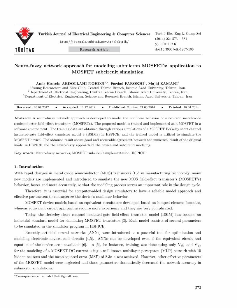
These stages are summarized as 3 layers for a feedforward NN and are shown in Figure 1.
w1
w15
in1
in7
in2
Rule1
Rule15
F
a
b
Fuzzification Defuzzification
Input layer
Hiddenlayer Output
layer
Figure 1. Neuro-fuzzy network architecture.
Actually, the w parameters are the center of the THEN part of the fuzzy rules and the tf and sig
parameters are the center and width of the IF part of the rules on the Gaussian fuzzy sets, where IF THEN
fuzzy rules are membership functions for input/output pairs of the fuzzy system that not only are not fixed,
but also these membership functions must be optimized using the free parameters in the learning process.
In this work, the input voltages (Vds , Vgs) and 5 BSIM effective parameters comprise the training input
features and the drain current (Id) as the desired output.
To reduce the runtime for the training program, the most effective parameters in the MOSFET drain
current simulation in HSPICE are determined by changing them ±10%, and the 5 most effective ones that
changed the drain current significantly are selected [13].
These BSIM-selected parameters are: TOX (gate oxide thickness), A2 (second nonsaturation factor),
VSAT (saturation velocity of the carrier at T = TREF = TNOM), VTHO (threshold voltage of the long
channel device at Vbs = 0 and small Vds), and DROUT (length dependence coefficient of the DIBL correction
parameter in rout). The drain current (Id) is created in HSPICE, while the input voltages are swept between
2 desired values.
3. Model validation and implementation into HSPICE
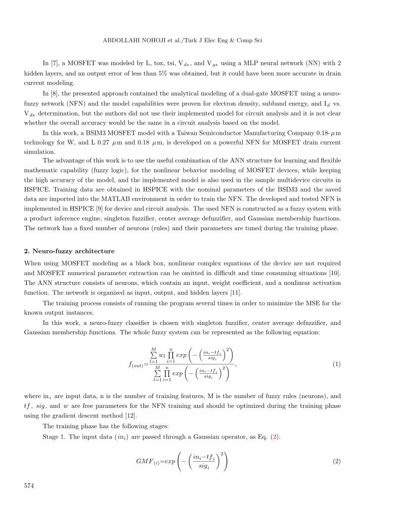
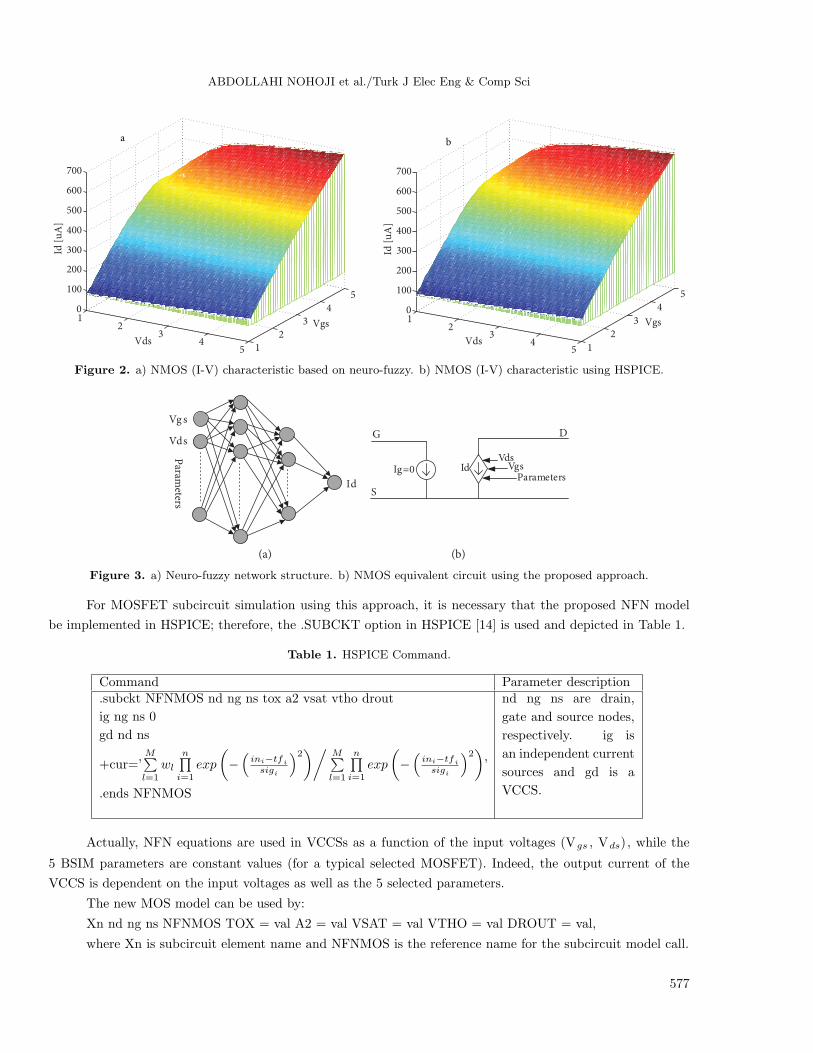
In order to show the NN generalization capabilities, the MOSFET NFN model can be utilized to predict the
drain current in different conditions. In Figures 2a and 2b, the characteristics of the neuro-fuzzy approach and
HSPICE model are shown for comparison, where the input voltages (Vgs , Vds) are swept between 1 and 5 V.
As it is clearly noticeable, there is a good agreement between the NFN and original HSPICE models’ (I–V)
characteristics.
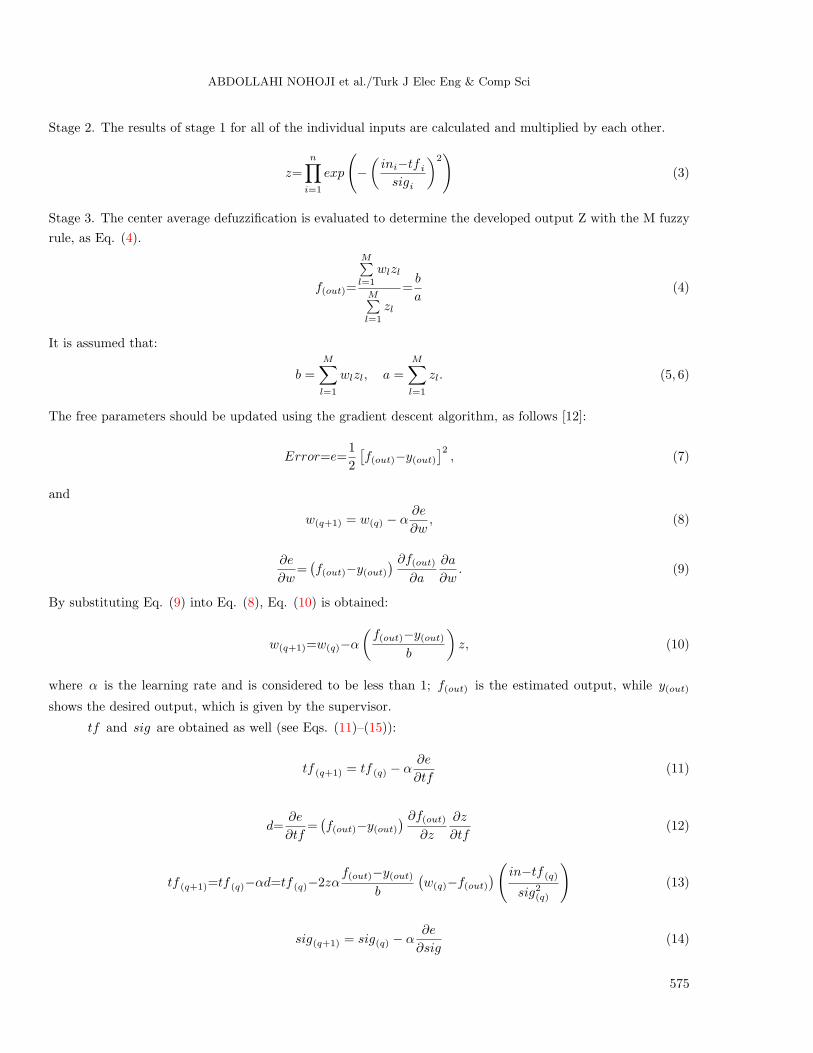
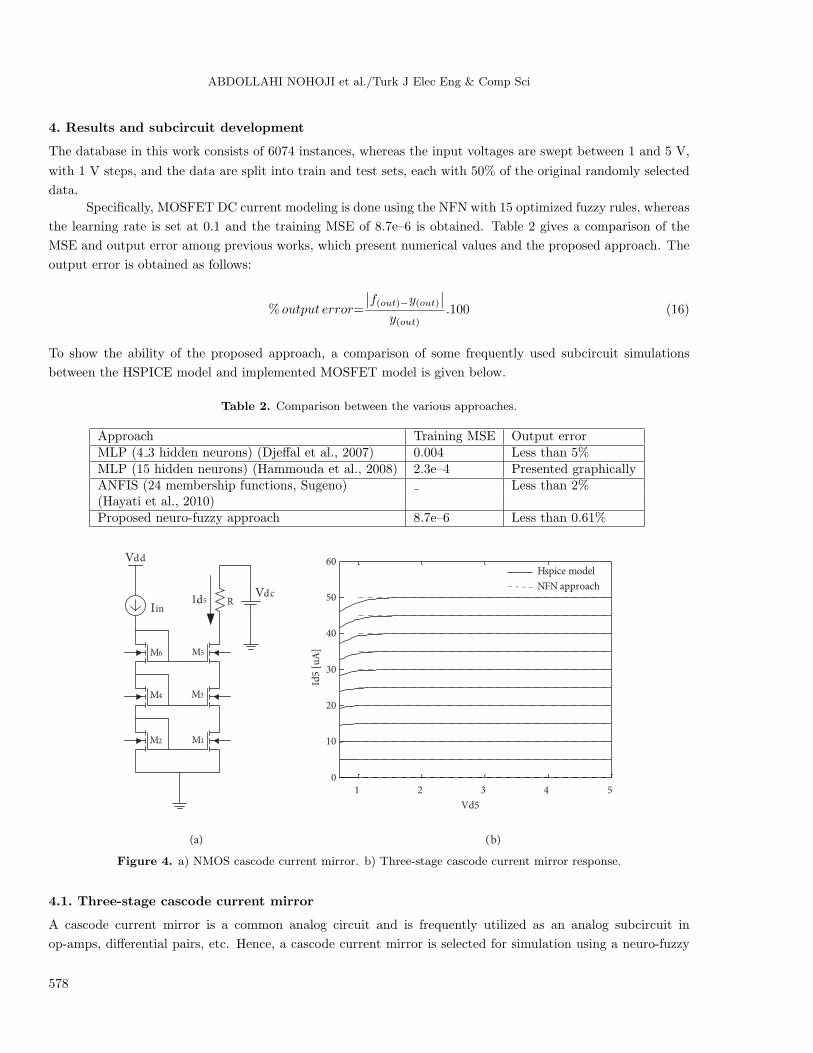
As mentioned previously, the proposed NFN model includes Vgs and Vds as input variables, whereas
the 5 BSIM parameters remain constant for each typical MOSFET technology. Therefore, the MOSFET drain
and gate currents based on the neuro-fuzzy approach could be considered as a voltage-controlled current source
(VCCS) and a null current source, respectively [1]. The NFN structure and negative-channel MOS (NMOS)
equivalent circuit of the proposed approach are shown in Figures 3a and 3b.
576
ABDOLLAHI NOHOJI et al./Turk J Elec Eng & Comp Sci
12
34
5 1
2
3
4
5
0
100
200
300
400
500
600
700
Vgs
Vds
Id [
uA
]
a
12
34
5 1
2
3
4
5
0
100
200
300
400
500
600
700
Vgs
Vds
Id [
uA
]
b
Figure 2. a) NMOS (I-V) characteristic based on neuro-fuzzy. b) NMOS (I-V) characteristic using HSPICE.
Vds
Vg s
Id
Ig=0Vds
VgsParameters
G
S
D
Id
Param
eters
(a) (b)
Figure 3. a) Neuro-fuzzy network structure. b) NMOS equivalent circuit using the proposed approach.
For MOSFET subcircuit simulation using this approach, it is necessary that the proposed NFN model
be implemented in HSPICE; therefore, the .SUBCKT option in HSPICE [14] is used and depicted in Table 1.
Table 1. HSPICE Command.
Command Parameter description.subckt NFNMOS nd ng ns tox a2 vsat vtho drout
ig ng ns 0
gd nd ns
+cur=’M∑l=1
wl
n∏i=1
exp
(−(
ini−tfi
sigi
)2)/ M∑l=1
n∏i=1
exp
(−(
ini−tfi
sigi
)2)’
.ends NFNMOS
nd ng ns are drain,
gate and source nodes,
respectively. ig is
an independent current
sources and gd is a
VCCS.
Actually, NFN equations are used in VCCSs as a function of the input voltages (Vgs , Vds), while the
5 BSIM parameters are constant values (for a typical selected MOSFET). Indeed, the output current of the
VCCS is dependent on the input voltages as well as the 5 selected parameters.
The new MOS model can be used by:
Xn nd ng ns NFNMOS TOX = val A2 = val VSAT = val VTHO = val DROUT = val,
where Xn is subcircuit element name and NFNMOS is the reference name for the subcircuit model call.
577
ABDOLLAHI NOHOJI et al./Turk J Elec Eng & Comp Sci
4. Results and subcircuit development
The database in this work consists of 6074 instances, whereas the input voltages are swept between 1 and 5 V,
with 1 V steps, and the data are split into train and test sets, each with 50% of the original randomly selected
data.
Specifically, MOSFET DC current modeling is done using the NFN with 15 optimized fuzzy rules, whereas
the learning rate is set at 0.1 and the training MSE of 8.7e–6 is obtained. Table 2 gives a comparison of the
MSE and output error among previous works, which present numerical values and the proposed approach. The
output error is obtained as follows:
% output error=
∣∣f(out)−y(out)∣∣y(out)
.100 (16)
To show the ability of the proposed approach, a comparison of some frequently used subcircuit simulations
between the HSPICE model and implemented MOSFET model is given below.
Table 2. Comparison between the various approaches.
Approach Training MSE Output errorMLP (4 3 hidden neurons) (Djeffal et al., 2007) 0.004 Less than 5%MLP (15 hidden neurons) (Hammouda et al., 2008) 2.3e–4 Presented graphicallyANFIS (24 membership functions, Sugeno) Less than 2%(Hayati et al., 2010)Proposed neuro-fuzzy approach 8.7e–6 Less than 0.61%
VdcR
Iin
M1M2
M3M4
M5M6
Vdd
Id5
(a) (b)
1 2 3 4 50
10
20
30
40
50
60
Vd5
Id5
[u
A]
Hspice model
NFN approach
Figure 4. a) NMOS cascode current mirror. b) Three-stage cascode current mirror response.
4.1. Three-stage cascode current mirror
A cascode current mirror is a common analog circuit and is frequently utilized as an analog subcircuit in
op-amps, differential pairs, etc. Hence, a cascode current mirror is selected for simulation using a neuro-fuzzy
578

ABDOLLAHI NOHOJI et al./Turk J Elec Eng & Comp Sci
MOSFET model instead of the HSPICE one. Vdc and I in are swept from 1 to 5 V and 0 to 50 µA, respectively.
A 3-stage cascode current mirror based on the NFN is shown in Figure 4a and the results of the HSPICE (solid
line) and neuro-fuzzy approach (dashed line) are given in Figure 4b for comparison.
4.2. Inversion property of NMOS
To show the inversion property of the NMOS, 3-stage cascade NMOS transistors (Figure 5) are simulated,
whereas a capacitance of 20 pf is placed as the C load. The input node is biased with a 2.2-V voltage source,
seri with an AC source, while each drain node is connected with a 10-k-ohm resistor to the 5 V DC power
supply.
10k10k 10k
5v
AC
2.2v
20pf
M1
M2M3
Vout
Vin
Figure 5. Three-stage cascade MOSFET transistors.
Figure 6 shows the results for both the original model in HSPICE and the NFN model for an input pulse
signal of 0.5 V for a period of 20 ns.
0 0.5 1 1.5 2 2.5 3 3.5 4 4.5 5
x 10-8
1.6
1.8
2
2.2
2.4
2.6
2.8
3
3.2
3.4
3.6
Time [s]
Vo
ltag
es [
v]
Vout(Hspice)Vout(NFN)Vin
Figure 6. Result of the 3-stage cascade NMOS inverter for the input pulse signal.
The response for the HSPICE (dashed line) and the neuro-fuzzy approach (solid line) for a sinusoidal
signal input of 0.5 V peak-to-peak and frequency of 50 MHz is given in Figure 7 as well.
579
ABDOLLAHI NOHOJI et al./Turk J Elec Eng & Comp Sci
(a) (b)
0 0.5 1 1.5 2 2.5 3 3.5 4 4.5 5x 10⁻⁸
1
1.5
2
2.5
3
3.5
4
Time [s]
Vo
ltag
es [
v]
Vout(Hspice)Vout(NFN)Vin
1 2 3 4 5 6 7 8 9x 10⁻⁹
2.6
2.7
2.8
2.9
3
3.1
3.2
3.3
3.4
Time [s]
Vo
ltag
es [
v]
Vout(Hspice)Vout(NFN)Vin
Figure 7. Three-stage cascode NMOS inverter simulation result for the sinusoidal signal: a) the whole signal and b)
zoomed view.
5. Conclusions
A dynamic (I-V) characteristic and accurately drain current modeling of a BSIM3 MOSFET is presented using
a NFN approach.
In this approach, the drain current is approximately obtained by an acceptable output error, better than
that in previous works, without using the conventional BSIM models and their parameters; they are normally
obtained by trial and error in model structures, which is a very time consuming and complicated process.
To show the accuracy of the proposed model, the results of some subcircuit simulations are presented,
which show an excellent agreement between the approaches used compared to HSPICE. The new MOSFET NFN
model is implemented in HSPICE using a VCCS and an independent current source structure for subcircuit
simulation.
As it is shown, the presented model could be used as a subcircuit as well and it may find some applications
for the modeling of new devices where mathematical equations and their parameters are not yet determined.
References
[1] R. Geiger, P. Allen, N. Strader, VLSI Design Techniques for Analog and Digital Circuits, New York, McGraw-Hill,
pp. 143–185, 544–548, 1990.
[2] J. Baker, CMOS Circuit Design, Layout and Simulation, New York, Wiley Interscience, pp. 131–161, 2005.
[3] H. Abebe, V.C. Tyree, “BSIM3v3.1 model parameters extraction and optimization”, USC-ISI the MOSIS Service
Technical Report, 2000.
[4] J.I. Ababneh, O. Qasaimeh, “Simple model for quantum-dot semiconductor optical amplifiers using artificial neural
networks”, IEEE Transactions on Electron Devices, Vol. 53, pp. 1543–1550, 2006.
[5] H.J. Delgado, M.H. Thursby, F.M. Ham, “A novel neural network for the synthesis of antennas and microwave
devices”, IEEE Transactions on Neural Networks, Vol. 16, pp. 1590–1600, 2005.
[6] H.B. Hammouda, M. Mhiri, Z. Gafsi, K. Besbes, “Neural-based models of semiconductor devices for SPICE
simulator”, American Journal of Applied Sciences, Vol. 5, pp. 385–391, 2008.
[7] F. Djeffal, M. Chahdi, A. Benhaya, M.L. Hafiane, “An approach based on neural computation to simulate the
nanoscale CMOS circuits: application to the simulation of CMOS inverter”, Elsevier Solid-State Electronics, Vol.
51, pp. 48–56, 2007.
[8] S. Chouhan, Y. Kumar, A. Chhipa, “Comparative study of DG-MOSFET modeling based on ANFIS and NEGF”,
International Journal of Engineering and Innovative Technology, Vol. 1, pp. 95–101, 2012.
580
ABDOLLAHI NOHOJI et al./Turk J Elec Eng & Comp Sci
[9] M. Hayati, M. Seifi, A. Rezaei, “Double gate MOSFET modeling based on adaptive neuro-fuzzy inference system
for nanoscale circuit simulation” Journal of Electronics and Telecommunications Research Institute, Vol. 32, pp.
530–539, 2010.
[10] P. Ojala, J. Saarinen, K. Kaski, “Device modeling for VLSI circuit design with technology independent NN
inference”, IEEE Proceedings of the 37th IEEE Midwest Symposium on Circuits and Systems, Vol. 1, pp. 688–693,
1994.
[11] S. Hatami, M.Y. Azizi, H.R. Bahrami, D. Motavalizadeh, A. Afzali-Kusha, “Accurate and efficient modeling of
SOI MOSFET with technology independent neural networks”, IEEE Transactions on Computer-Aided Design of
Integrated Circuits and Systems, Vol. 23, pp. 1580–1587, 2004.
[12] L.X. Wang, A Course in Fuzzy System and Control, Englewood Cliffs, Prentice Hall, 1996.
[13] A.H.A. Nohoji, F. Farokhi, M. Shokouhifar, M. Zamani, “Efficient parameters selection for artificial intelligence
models of nanoscale MOSFETs”, IEEE Proceedingsof the 24th Canadian Conference on Electrical and Computer
Engineering, pp. 840–844, 2011.
[14] HSPICE Command Reference Version W-2005.03, Synopsys, Inc., 2005.
581


![Spice Subcircuit Support for Serial Link Channel Design ... · HUAWEI TECHNOLOGIES CO., ... Spice Subcircuit Support for Serial Link Channel Design Using IBIS [External Model] IBIS](https://img.dokumen.tips/doc/110x75/5b2b25877f8b9af1088b57b5/spice-subcircuit-support-for-serial-link-channel-design-huawei-technologies.jpg)