Embed Size (px)
Citation preview
DISTRIBUTION STATEMENT A: Approved for public release; distribution is unlimited.
NONRESIDENTTRAININGCOURSE
SEPTEMBER 1998
Navy Electricity andElectronics Training Series
Module 12—Modulation
NAVEDTRA 14184

DISTRIBUTION STATEMENT A: Approved for public release; distribution is unlimited.
Although the words “he,” “him,” and“his” are used sparingly in this course toenhance communication, they are notintended to be gender driven or to affront ordiscriminate against anyone.

i
PREFACE
By enrolling in this self-study course, you have demonstrated a desire to improve yourself and the Navy.Remember, however, this self-study course is only one part of the total Navy training program. Practicalexperience, schools, selected reading, and your desire to succeed are also necessary to successfully roundout a fully meaningful training program.
COURSE OVERVIEW : To introduce the student to the subject of Modulation Principles who needssuch a background in accomplishing daily work and/or in preparing for further study.
THE COURSE: This self-study course is organized into subject matter areas, each containing learningobjectives to help you determine what you should learn along with text and illustrations to help youunderstand the information. The subject matter reflects day-to-day requirements and experiences ofpersonnel in the rating or skill area. It also reflects guidance provided by Enlisted Community Managers(ECMs) and other senior personnel, technical references, instructions, etc., and either the occupational ornaval standards, which are listed in theManual of Navy Enlisted Manpower Personnel Classificationsand Occupational Standards, NAVPERS 18068.
THE QUESTIONS: The questions that appear in this course are designed to help you understand thematerial in the text.
VALUE : In completing this course, you will improve your military and professional knowledge.Importantly, it can also help you study for the Navy-wide advancement in rate examination. If you arestudying and discover a reference in the text to another publication for further information, look it up.
1998 Edition Prepared byETCM Danny K. Krutson
Published byNAVAL EDUCATION AND TRAINING
PROFESSIONAL DEVELOPMENTAND TECHNOLOGY CENTER
NAVSUP Logistics Tracking Number0504-LP-026-8370

ii
Sailor’s Creed
“ I am a United States Sailor.
I will support and defend theConstitution of the United States ofAmerica and I will obey the ordersof those appointed over me.
I represent the fighting spirit of theNavy and those who have gonebefore me to defend freedom anddemocracy around the world.
I proudly serve my country’s Navycombat team with honor, courageand commitment.
I am committed to excellence andthe fair treatment of all.”
iii
TABLE OF CONTENTS
CHAPTER PAGE
1. Amplitude Modulation ............................................................................................. 1-1
2. Angle and Pulse Modulation .................................................................................... 2-1
3. Demodulation ........................................................................................................... 3-1
APPENDIX
I. Glossary.................................................................................................................. AI-1
INDEX ......................................................................................................................... INDEX-1
iv
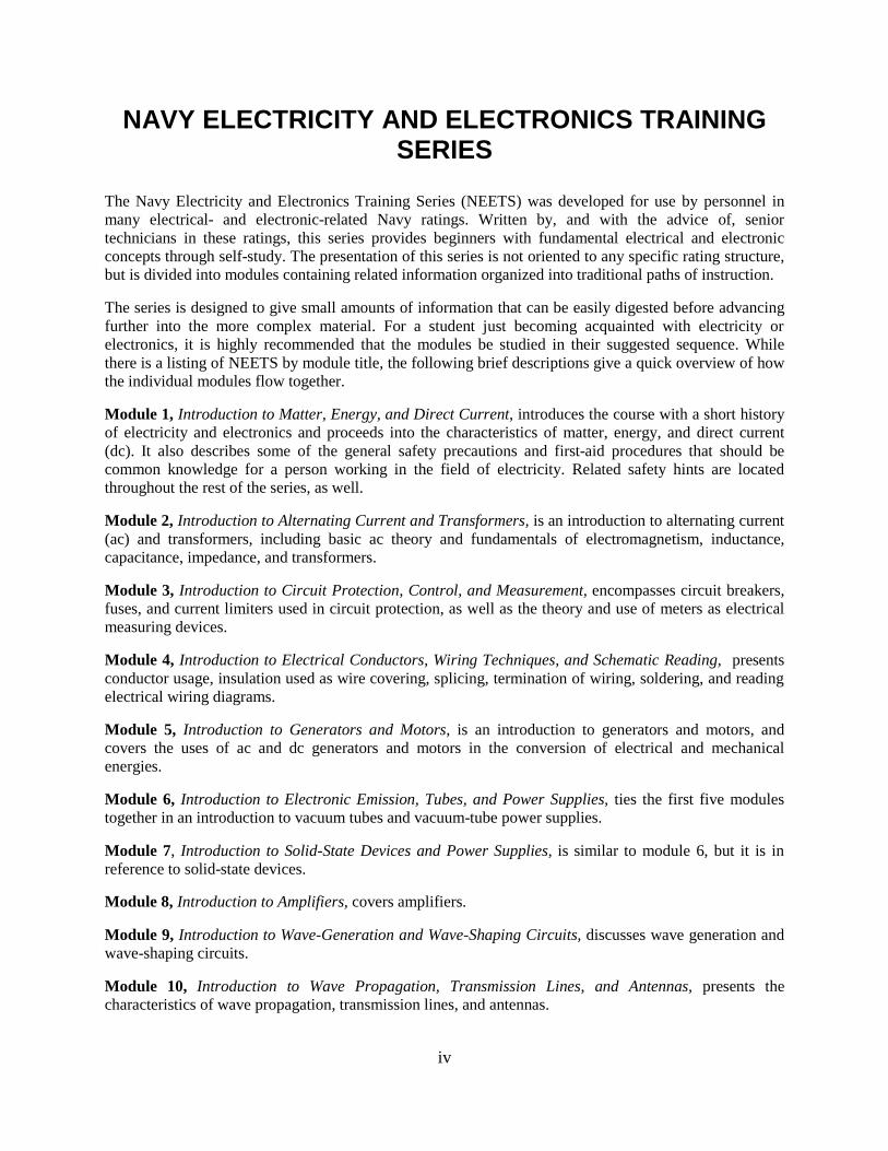
NAVY ELECTRICITY AND ELECTRONICS TRAININGSERIES
The Navy Electricity and Electronics Training Series (NEETS) was developed for use by personnel inmany electrical- and electronic-related Navy ratings. Written by, and with the advice of, seniortechnicians in these ratings, this series provides beginners with fundamental electrical and electronicconcepts through self-study. The presentation of this series is not oriented to any specific rating structure,but is divided into modules containing related information organized into traditional paths of instruction.
The series is designed to give small amounts of information that can be easily digested before advancingfurther into the more complex material. For a student just becoming acquainted with electricity orelectronics, it is highly recommended that the modules be studied in their suggested sequence. Whilethere is a listing of NEETS by module title, the following brief descriptions give a quick overview of howthe individual modules flow together.
Module 1, Introduction to Matter, Energy, and Direct Current, introduces the course with a short historyof electricity and electronics and proceeds into the characteristics of matter, energy, and direct current(dc). It also describes some of the general safety precautions and first-aid procedures that should becommon knowledge for a person working in the field of electricity. Related safety hints are locatedthroughout the rest of the series, as well.
Module 2, Introduction to Alternating Current and Transformers,is an introduction to alternating current(ac) and transformers, including basic ac theory and fundamentals of electromagnetism, inductance,capacitance, impedance, and transformers.
Module 3, Introduction to Circuit Protection, Control, and Measurement,encompasses circuit breakers,fuses, and current limiters used in circuit protection, as well as the theory and use of meters as electricalmeasuring devices.
Module 4, Introduction to Electrical Conductors, Wiring Techniques, and Schematic Reading,presentsconductor usage, insulation used as wire covering, splicing, termination of wiring, soldering, and readingelectrical wiring diagrams.
Module 5, Introduction to Generators and Motors,is an introduction to generators and motors, andcovers the uses of ac and dc generators and motors in the conversion of electrical and mechanicalenergies.
Module 6, Introduction to Electronic Emission, Tubes, and Power Supplies,ties the first five modulestogether in an introduction to vacuum tubes and vacuum-tube power supplies.
Module 7, Introduction to Solid-State Devices and Power Supplies,is similar to module 6, but it is inreference to solid-state devices.
Module 8, Introduction to Amplifiers,covers amplifiers.
Module 9, Introduction to Wave-Generation and Wave-Shaping Circuits,discusses wave generation andwave-shaping circuits.
Module 10, Introduction to Wave Propagation, Transmission Lines, and Antennas,presents thecharacteristics of wave propagation, transmission lines, and antennas.
v
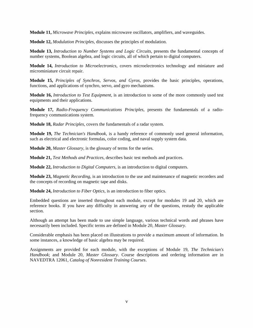
Module 11,Microwave Principles,explains microwave oscillators, amplifiers, and waveguides.
Module 12,Modulation Principles,discusses the principles of modulation.
Module 13, Introduction to Number Systems and Logic Circuits,presents the fundamental concepts ofnumber systems, Boolean algebra, and logic circuits, all of which pertain to digital computers.
Module 14, Introduction to Microelectronics,covers microelectronics technology and miniature andmicrominiature circuit repair.
Module 15, Principles of Synchros, Servos, and Gyros,provides the basic principles, operations,functions, and applications of synchro, servo, and gyro mechanisms.
Module 16, Introduction to Test Equipment,is an introduction to some of the more commonly used testequipments and their applications.
Module 17, Radio-Frequency Communications Principles,presents the fundamentals of a radio-frequency communications system.
Module 18,Radar Principles,covers the fundamentals of a radar system.
Module 19, The Technician's Handbook,is a handy reference of commonly used general information,such as electrical and electronic formulas, color coding, and naval supply system data.
Module 20,Master Glossary,is the glossary of terms for the series.
Module 21,Test Methods and Practices,describes basic test methods and practices.
Module 22, Introduction to Digital Computers,is an introduction to digital computers.
Module 23,Magnetic Recording,is an introduction to the use and maintenance of magnetic recorders andthe concepts of recording on magnetic tape and disks.
Module 24, Introduction to Fiber Optics,is an introduction to fiber optics.
Embedded questions are inserted throughout each module, except for modules 19 and 20, which arereference books. If you have any difficulty in answering any of the questions, restudy the applicablesection.
Although an attempt has been made to use simple language, various technical words and phrases havenecessarily been included. Specific terms are defined in Module 20,Master Glossary.
Considerable emphasis has been placed on illustrations to provide a maximum amount of information. Insome instances, a knowledge of basic algebra may be required.
Assignments are provided for each module, with the exceptions of Module 19,The Technician'sHandbook; and Module 20,Master Glossary. Course descriptions and ordering information are inNAVEDTRA 12061,Catalog of Nonresident Training Courses.
vi
Throughout the text of this course and while using technical manuals associated with the equipment youwill be working on, you will find the below notations at the end of some paragraphs. The notations areused to emphasize that safety hazards exist and care must be taken or observed.
WARNING
AN OPERATING PROCEDURE, PRACTICE, OR CONDITION, ETC., WHICH MAYRESULT IN INJURY OR DEATH IF NOT CAREFULLY OBSERVED ORFOLLOWED.
CAUTION
AN OPERATING PROCEDURE, PRACTICE, OR CONDITION, ETC., WHICH MAYRESULT IN DAMAGE TO EQUIPMENT IF NOT CAREFULLY OBSERVED ORFOLLOWED.
NOTE
An operating procedure, practice, or condition, etc., which is essential to emphasize.
vii
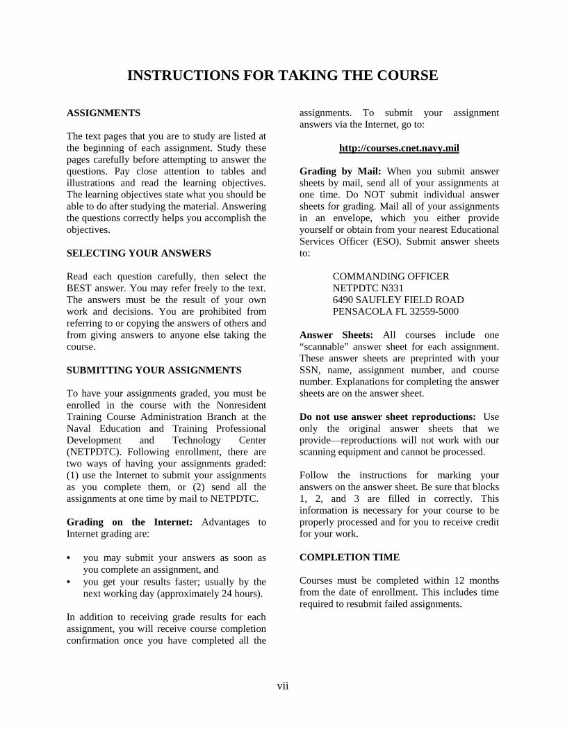
INSTRUCTIONS FOR TAKING THE COURSE
ASSIGNMENTS
The text pages that you are to study are listed atthe beginning of each assignment. Study thesepages carefully before attempting to answer thequestions. Pay close attention to tables andillustrations and read the learning objectives.The learning objectives state what you should beable to do after studying the material. Answeringthe questions correctly helps you accomplish theobjectives.
SELECTING YOUR ANSWERS
Read each question carefully, then select theBEST answer. You may refer freely to the text.The answers must be the result of your ownwork and decisions. You are prohibited fromreferring to or copying the answers of others andfrom giving answers to anyone else taking thecourse.
SUBMITTING YOUR ASSIGNMENTS
To have your assignments graded, you must beenrolled in the course with the NonresidentTraining Course Administration Branch at theNaval Education and Training ProfessionalDevelopment and Technology Center(NETPDTC). Following enrollment, there aretwo ways of having your assignments graded:(1) use the Internet to submit your assignmentsas you complete them, or (2) send all theassignments at one time by mail to NETPDTC.
Grading on the Internet: Advantages toInternet grading are:
• you may submit your answers as soon asyou complete an assignment, and
• you get your results faster; usually by thenext working day (approximately 24 hours).
In addition to receiving grade results for eachassignment, you will receive course completionconfirmation once you have completed all the
assignments. To submit your assignmentanswers via the Internet, go to:
http://courses.cnet.navy.mil
Grading by Mail: When you submit answersheets by mail, send all of your assignments atone time. Do NOT submit individual answersheets for grading. Mail all of your assignmentsin an envelope, which you either provideyourself or obtain from your nearest EducationalServices Officer (ESO). Submit answer sheetsto:
COMMANDING OFFICERNETPDTC N3316490 SAUFLEY FIELD ROADPENSACOLA FL 32559-5000
Answer Sheets: All courses include one“scannable” answer sheet for each assignment.These answer sheets are preprinted with yourSSN, name, assignment number, and coursenumber. Explanations for completing the answersheets are on the answer sheet.
Do not use answer sheet reproductions:Useonly the original answer sheets that weprovide—reproductions will not work with ourscanning equipment and cannot be processed.
Follow the instructions for marking youranswers on the answer sheet. Be sure that blocks1, 2, and 3 are filled in correctly. Thisinformation is necessary for your course to beproperly processed and for you to receive creditfor your work.
COMPLETION TIME
Courses must be completed within 12 monthsfrom the date of enrollment. This includes timerequired to resubmit failed assignments.

viii
PASS/FAIL ASSIGNMENT PROCEDURES
If your overall course score is 3.2 or higher, youwill pass the course and will not be required toresubmit assignments. Once your assignmentshave been graded you will receive coursecompletion confirmation.
If you receive less than a 3.2 on any assignmentand your overall course score is below 3.2, youwill be given the opportunity to resubmit failedassignments. You may resubmit failedassignments only once. Internet students willreceive notification when they have failed anassignment--they may then resubmit failedassignments on the web site. Internet studentsmay view and print results for failedassignments from the web site. Students whosubmit by mail will receive a failing result letterand a new answer sheet for resubmission of eachfailed assignment.
COMPLETION CONFIRMATION
After successfully completing this course, youwill receive a letter of completion.
ERRATA
Errata are used to correct minor errors or deleteobsolete information in a course. Errata mayalso be used to provide instructions to thestudent. If a course has an errata, it will beincluded as the first page(s) after the front cover.Errata for all courses can be accessed andviewed/downloaded at:
http://www.advancement.cnet.navy.mil
STUDENT FEEDBACK QUESTIONS
We value your suggestions, questions, andcriticisms on our courses. If you would like tocommunicate with us regarding this course, weencourage you, if possible, to use e-mail. If youwrite or fax, please use a copy of the StudentComment form that follows this page.
For subject matter questions:
E-mail: [email protected]: Comm: (850) 452-1001, ext. 1728
DSN: 922-1001, ext. 1728FAX: (850) 452-1370(Do not fax answer sheets.)
Address: COMMANDING OFFICERNETPDTC N3156490 SAUFLEY FIELD ROADPENSACOLA FL 32509-5237
For enrollment, shipping, grading, orcompletion letter questions
E-mail: [email protected]: Toll Free: 877-264-8583
Comm: (850) 452-1511/1181/1859DSN: 922-1511/1181/1859FAX: (850) 452-1370(Do not fax answer sheets.)
Address: COMMANDING OFFICERNETPDTC N3316490 SAUFLEY FIELD ROADPENSACOLA FL 32559-5000
NAVAL RESERVE RETIREMENT CREDIT
If you are a member of the Naval Reserve, youwill receive retirement points if you areauthorized to receive them under currentdirectives governing retirement of NavalReserve personnel. For Naval Reserveretirement, this course is evaluated at 7 points.(Refer to Administrative Procedures for NavalReservists on Inactive Duty,BUPERSINST1001.39, for more information about retirementpoints.)
ix
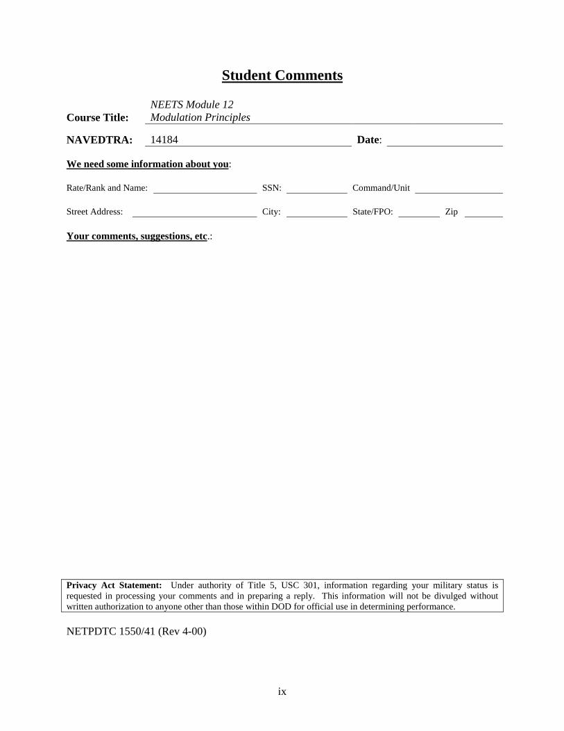
Student Comments
Course Title:NEETS Module 12Modulation Principles
NAVEDTRA: 14184 Date:
We need some information about you:
Rate/Rank and Name: SSN: Command/Unit
Street Address: City: State/FPO: Zip
Your comments, suggestions, etc.:
Privacy Act Statement: Under authority of Title 5, USC 301, information regarding your military status isrequested in processing your comments and in preparing a reply. This information will not be divulged withoutwritten authorization to anyone other than those within DOD for official use in determining performance.
NETPDTC 1550/41 (Rev 4-00)

1-1
CHAPTER 1
AMPLITUDE MODULATION
LEARNING OBJECTIVES
Learning objectives are stated at the beginning of each chapter. These learning objectives serve as a preview of the information you are expected to learn in the chapter. The comprehensive check questions are based on the objectives. By successfully completing the OCC/ECC, you indicate that you have met the objectives and have learned the information. The learning objectives are listed below.
Upon completion of this chapter, you will be able to:
1. Discuss the generation of a sine wave by describing its three characteristics: amplitude, phase, and frequency.
2. Describe the process of heterodyning.
3. Discuss the development of continuous-wave (cw) modulation.
4. Describe the two primary methods of cw communications keying.
5. Discuss the radio frequency (rf) spectrum usage by cw transmissions.
6. Discuss the advantages and disadvantages of cw transmissions.
7. Explain the operation of typical cw transmitter circuitry.
8. Discuss the method of changing sound waves into electrical impulses.
9. Describe the rf usage of an AM signal.
10. Calculate the percent of modulation for an AM signal.
11. Discuss the difference between high- and low-level modulation.
12. Describe the circuit description, operation, advantages, and disadvantages of the following common AM tube/transistor modulating circuits: plate/collector, control grid/base, and cathode/emitter.
13. Discuss the advantages and disadvantages of AM communications.
INTRODUCTION TO MODULATION PRINCIPLES
People have always had the desire to communicate their ideas to others. Communications have not only been desired from a social point of view, but have been an essential element in the building of civilization. Through communications, people have been able to share ideas of mutual benefit to all mankind. Early attempts to maintain communications between distant points were limited by several factors. For example, the relatively short distance sound would carry and the difficulty of hand-carrying messages over great distances hampered effective communications.

1-2
As the potential for the uses of electricity were explored, scientists in the United States and England worked to develop the telegraph. The first practical system was established in London, England, in 1838. Just 20 years later, the final link to connect the major countries with electrical communications was completed when a transatlantic submarine cable was connected. Commercial telegraphy was practically worldwide by 1890. The telegraph key, wire lines, and Morse code made possible almost instantaneous communications between points at great distances. Submarine cables solved the problems of transoceanic communications, but communications with ships at sea and mobile forces were still poor.
In 1897 Marconi demonstrated the first practical wireless transmitter. He sent and received messages over a distance of 8 miles. By 1898 he had demonstrated the usefulness of wireless telegraph communications at sea. In 1899 he established a wireless telegraphic link across the English Channel. His company also established general usage of the wireless telegraph between coastal light ships (floating lighthouses) and land. The first successful transatlantic transmissions were achieved in 1902. From that time to the present, radio communication has grown at an extraordinary rate. Early systems transmitted a few words per minute with doubtful reliability. Today, communications systems reliably transmit information across millions of miles.
The desire to communicate directly by voice, at a higher rate of speed than possible through basic telegraphy, led to further research. That research led to the development of MODULATION. Modulation is the ability to impress intelligence upon a TRANSMISSION MEDIUM, such as radio waves. A transmission medium can be described as light, smoke, sound, wire lines, or radio-frequency waves. In this module, you will study the basic principles of modulation and DEMODULATION (removing intelligence from the medium).
In your studies, you will learn about modulation as it applies to radio-frequency communications. To modulate is to impress the characteristics (intelligence) of one waveform onto a second waveform by varying the amplitude, frequency, phase, or other characteristics of the second waveform. First, however, you will review the characteristics and generation of a sine wave. This review will help you to better understand the principles of modulation. Then, an important principle called HETERODYNING (mixing two frequencies across a nonlinear impedance) will be studied and applied to modulation. Nonlinear impedance will be discussed in the heterodyning section. You will also study several methods of modulating a radio-frequency carrier. You will come to a better understanding of the demodulation principle by studying the various circuits used to demodulate a modulated carrier.
Q-1. What is modulation?
Q-2. What is a transmission medium?
Q-3. What is heterodyning?
Q-4. What is demodulation?
SINE WAVE CHARACTERISTICS
The basic alternating waveform for all complex waveforms is the sine wave. Therefore, an understanding of sine wave characteristics and how they can be acted upon is essential for you to understand modulation. You may want to review sine waves in chapter 1 of NEETS, Module 2, Introduction to Alternating Current and Transformers at this point.
1-3
GENERATION OF SINE WAVES
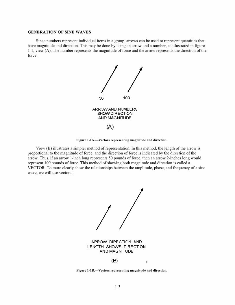
Since numbers represent individual items in a group, arrows can be used to represent quantities that have magnitude and direction. This may be done by using an arrow and a number, as illustrated in figure 1-1, view (A). The number represents the magnitude of force and the arrow represents the direction of the force.
Figure 1-1A.—Vectors representing magnitude and direction.
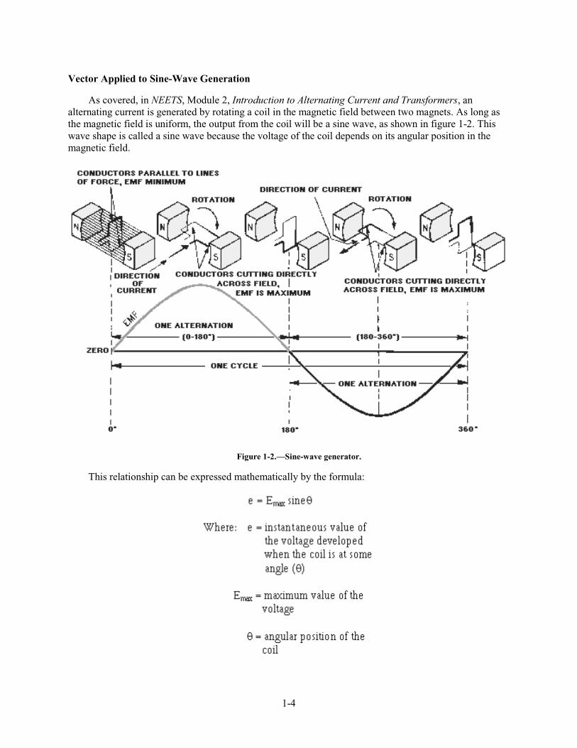
View (B) illustrates a simpler method of representation. In this method, the length of the arrow is proportional to the magnitude of force, and the direction of force is indicated by the direction of the arrow. Thus, if an arrow 1-inch long represents 50 pounds of force, then an arrow 2-inches long would represent 100 pounds of force. This method of showing both magnitude and direction is called a VECTOR. To more clearly show the relationships between the amplitude, phase, and frequency of a sine wave, we will use vectors.
+
Figure 1-1B.—Vectors representing magnitude and direction.
1-4
Vector Applied to Sine-Wave Generation
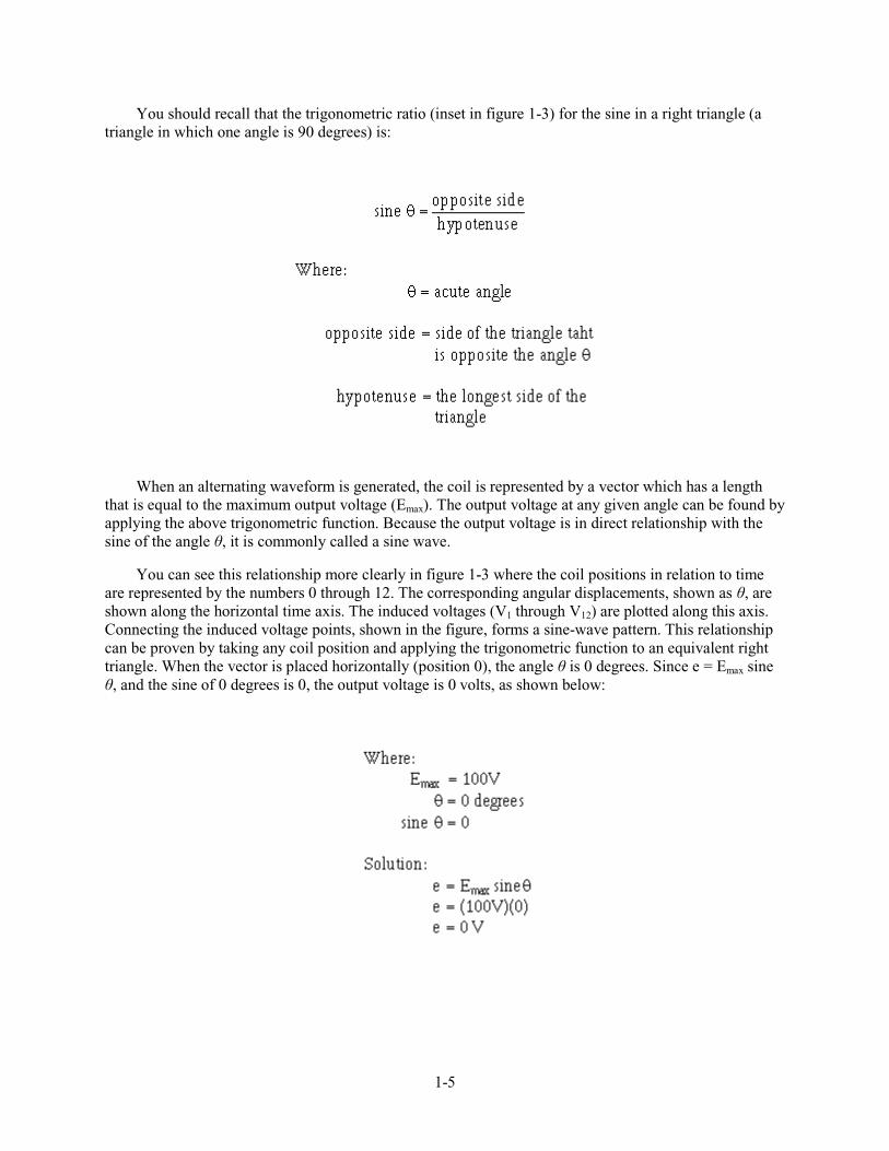
As covered, in NEETS, Module 2, Introduction to Alternating Current and Transformers, an alternating current is generated by rotating a coil in the magnetic field between two magnets. As long as the magnetic field is uniform, the output from the coil will be a sine wave, as shown in figure 1-2. This wave shape is called a sine wave because the voltage of the coil depends on its angular position in the magnetic field.
Figure 1-2.—Sine-wave generator.
This relationship can be expressed mathematically by the formula:
1-5
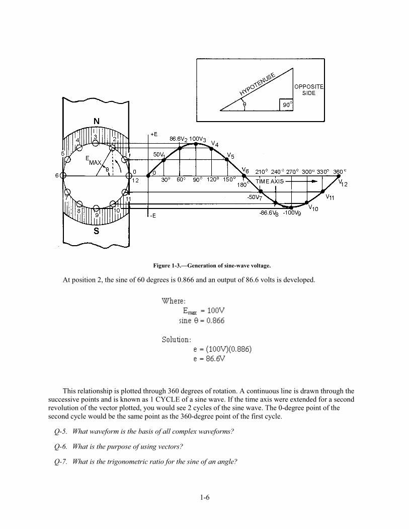
You should recall that the trigonometric ratio (inset in figure 1-3) for the sine in a right triangle (a triangle in which one angle is 90 degrees) is:
When an alternating waveform is generated, the coil is represented by a vector which has a length that is equal to the maximum output voltage (Emax). The output voltage at any given angle can be found by applying the above trigonometric function. Because the output voltage is in direct relationship with the sine of the angle !, it is commonly called a sine wave.
You can see this relationship more clearly in figure 1-3 where the coil positions in relation to time are represented by the numbers 0 through 12. The corresponding angular displacements, shown as !, are shown along the horizontal time axis. The induced voltages (V1 through V12) are plotted along this axis. Connecting the induced voltage points, shown in the figure, forms a sine-wave pattern. This relationship can be proven by taking any coil position and applying the trigonometric function to an equivalent right triangle. When the vector is placed horizontally (position 0), the angle ! is 0 degrees. Since e = Emax sine !, and the sine of 0 degrees is 0, the output voltage is 0 volts, as shown below:
1-6
Figure 1-3.—Generation of sine-wave voltage.
At position 2, the sine of 60 degrees is 0.866 and an output of 86.6 volts is developed.
This relationship is plotted through 360 degrees of rotation. A continuous line is drawn through the successive points and is known as 1 CYCLE of a sine wave. If the time axis were extended for a second revolution of the vector plotted, you would see 2 cycles of the sine wave. The 0-degree point of the second cycle would be the same point as the 360-degree point of the first cycle.
Q-5. What waveform is the basis of all complex waveforms?
Q-6. What is the purpose of using vectors?
Q-7. What is the trigonometric ratio for the sine of an angle?

1-7
Q-8. What is the mathematical formula for computing the output voltage from a moving coil in a magnetic field?
AMPLITUDE
A sine wave is used to represent values of electrical current or voltage. The greater its height, the greater the value it represents. As you have studied, a sine wave alternately rises above and then falls below the reference line. That part above the line represents a positive value and is referred to as a POSITIVE ALTERNATION. That part of the cycle below the line has a negative value and is referred to as a NEGATIVE ALTERNATION. The maximum value, above or below the reference line, is called the PEAK AMPLITUDE. The value at any given point along the reference line is called the INSTANTANEOUS AMPLITUDE.
PHASE
PHASE or PHASE ANGLE indicates how much of a cycle has been completed at any given instant. This merely describes the angle that exists between the starting point of the vector and its position at that instant. The number of degrees of vector rotation and the number of degrees of the resultant sine wave that have been completed will be the same. For example, at time position 2 of figure 1-3, the vector has rotated to 60 degrees and 60 degrees of the resultant sine wave has been completed. Therefore, both are said to have an instantaneous phase angle of 60 degrees.
FREQUENCY
The rate at which the vector rotates determines the FREQUENCY of the sine wave that is generated; that is, the faster the vector rotates, the more cycles completed in a given time period. The basic time period used is 1 second. If a vector completes one revolution per 1 second, the resultant sine wave has a frequency 1 cycle per second (1 hertz). If the rate of rotation is increased to 1,000 revolutions per second, the frequency of the sine wave generated will be 1,000 cycles per second (1 kilohertz).
PERIOD
Another term that is important in the discussion of a sine wave is its duration, or PERIOD. The period of a cycle is the elapsed time from the beginning of a cycle to its completion. If the vector shown in figure 1-3 were to make 1 revolution per second, each cycle of the resultant sine wave would have a period of 1 second. If it were rotating at a speed of 1,000 revolutions per second, each revolution would require 1/1,000 of a second and the period of the resultant sine wave would be 1/1,000 of a second. This illustrates that the period is related to the frequency. As the number of cycles completed in 1 second increases, the period of each cycle will decrease proportionally. This relationship is shown in the following formulas:
1-8
WAVELENGTH
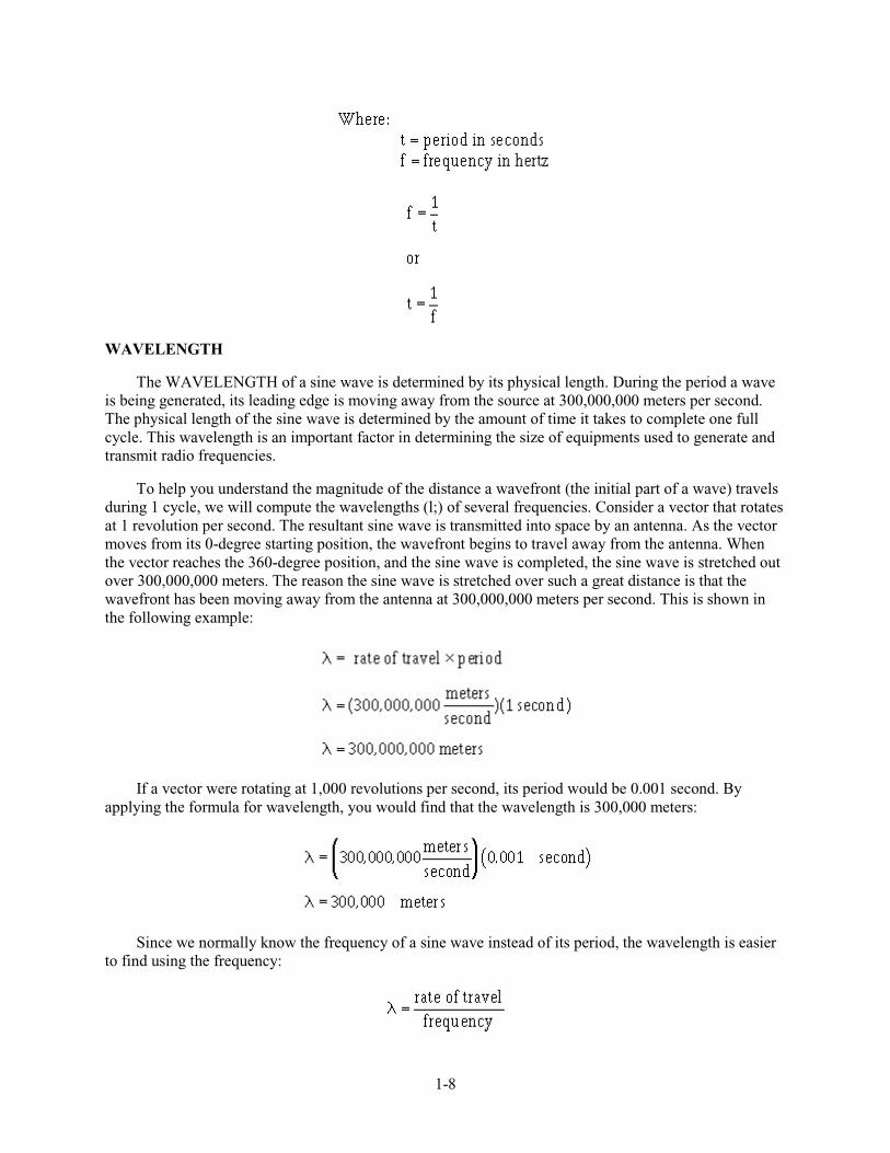
The WAVELENGTH of a sine wave is determined by its physical length. During the period a wave is being generated, its leading edge is moving away from the source at 300,000,000 meters per second. The physical length of the sine wave is determined by the amount of time it takes to complete one full cycle. This wavelength is an important factor in determining the size of equipments used to generate and transmit radio frequencies.
To help you understand the magnitude of the distance a wavefront (the initial part of a wave) travels during 1 cycle, we will compute the wavelengths (l;) of several frequencies. Consider a vector that rotates at 1 revolution per second. The resultant sine wave is transmitted into space by an antenna. As the vector moves from its 0-degree starting position, the wavefront begins to travel away from the antenna. When the vector reaches the 360-degree position, and the sine wave is completed, the sine wave is stretched out over 300,000,000 meters. The reason the sine wave is stretched over such a great distance is that the wavefront has been moving away from the antenna at 300,000,000 meters per second. This is shown in the following example:
If a vector were rotating at 1,000 revolutions per second, its period would be 0.001 second. By applying the formula for wavelength, you would find that the wavelength is 300,000 meters:
Since we normally know the frequency of a sine wave instead of its period, the wavelength is easier to find using the frequency:
1-9
Thus, for a sine wave with a frequency of 1,000,000 hertz (1 megahertz), the wavelength would be 300 meters, as shown below:
The higher the frequency, the shorter the wavelength of a sine wave. This important relationship between frequency and wavelength is illustrated in table 1-1.
Table 1-1.—Radio frequency versus wavelength
FREQUENCY WAVELENGTH METRIC U.S.
300,000 MHz .001 m .04 in EHF-
30,000 MHz .01 m .39 in SHF-
3,000 MHz .1 m 3.94 in UHF--
300 MHz 1 m 39.37 in VHF---
30 MHz 10 m 10.93 yd HF----
3 MHz 100 m 109.4 yd MF----
300 kHz 1 km .62 mi LF----
30 kHz 10 km 6.2 mi VLF-----
3 kHz 100 km 62 mi
Q-9. What is the instantaneous amplitude of a sine wave?
Q-10. What term describes how much of a cycle has been completed?
Q-11. What determines the frequency of a sine wave?
Q-12. What is the period of a cycle?

1-10
Q-13. How do you calculate the wavelength of a sine wave?
HETERODYNING
Information waveforms are produced by many different sources and are generally quite low in frequency. A good example is the human voice. The frequencies involved in normal speech vary from one individual to another and cover a wide range. This range can be anywhere from a low of about 90 hertz for a deep bass to as high as 10 kilohertz for a high soprano.
The most important speech frequencies almost entirely fall below 3 kilohertz. Higher frequencies merely help to achieve more perfect sound production. The range of frequencies used to transmit voice intelligence over radio circuits depends on the degree of FIDELITY (the ability to faithfully reproduce the input in the output) that is desired. The minimum frequency range that can be used for the transmission of speech is 500 to 2,000 hertz. The average range used on radiotelephone circuits is 250 to 2,750 hertz.
Frequencies contained within the human voice can be transmitted over telephone lines without difficulty, but transmitting them via radio circuits is not practical. This is because of their extremely long wavelengths and the fact that antennas would have to be constructed with long physical dimensions to transmit or radiate these wavelengths. Generally, antennas have radiating elements that are 1/4, 1/2, 1, or more full wavelengths of the frequency to be radiated. The wavelengths of voice frequencies employed on radiotelephone circuits range from 1,200,000 meters at 250 hertz to 109,090 meters at 2,750 hertz. Even a quarter-wave antenna would require a large area, be expensive to construct, and consume enormous amounts of power.
As studied in NEETS, Module 10, Introduction to Wave Propagation, Transmission Lines, and
Antennas, radio frequencies do not have the limitations just described for voice frequencies. Radio waves, given a suitable antenna, can often radiate millions of miles into space. Several methods of modulation can be used to impress voices frequencies onto radio waves for transmission through space.
In the modulation process, waves from the information source are impressed onto a radio-frequency sine wave called a CARRIER. This carrier is sufficiently high in frequency to have a wavelength short enough to be radiated from an antenna of practical dimensions. For example, a carrier frequency of 10 megahertz has a wavelength of 30 meters, as shown below:
Construction of an antenna related to that wavelength does not cause any problems.
An information wave is normally referred to as a MODULATING WAVE. When a modulating wave is impressed on a carrier, the voltages of the modulating wave and the carrier are combined in such a manner as to produce a COMPLEX WAVE (a wave composed of two or more parts). This complex wave
1-11
is referred to as the MODULATED WAVE and is the waveform that is transmitted through space. When the modulated wave is received and demodulated, the original component waves (carrier and modulating waves) are reproduced with their respective frequencies, phases, and amplitudes unchanged.
Modulation of a carrier can be achieved by any of several methods. Generally, the methods are named for the sine-wave characteristic that is altered by the modulation process. In this module, you will study AMPLITUDE MODULATION, which includes CONTINUOUS-WAVE MODULATION. You will also learn about two forms of ANGLE MODULATION (FREQUENCY MODULATION and PHASE MODULATION). A special type of modulation, known as PULSE MODULATION, will also be discussed. Before we present the methods involved in developing modulation, you need to study a process that is essential to the modulation of a carrier, known as heterodyning.
To help you understand the operation of heterodyning circuits, we will begin with a discussion of LINEAR and NONLINEAR devices. In linear devices, the output rises and falls directly with the input. In nonlinear devices, the output does not rise and fall directly with the input.
LINEAR IMPEDANCE
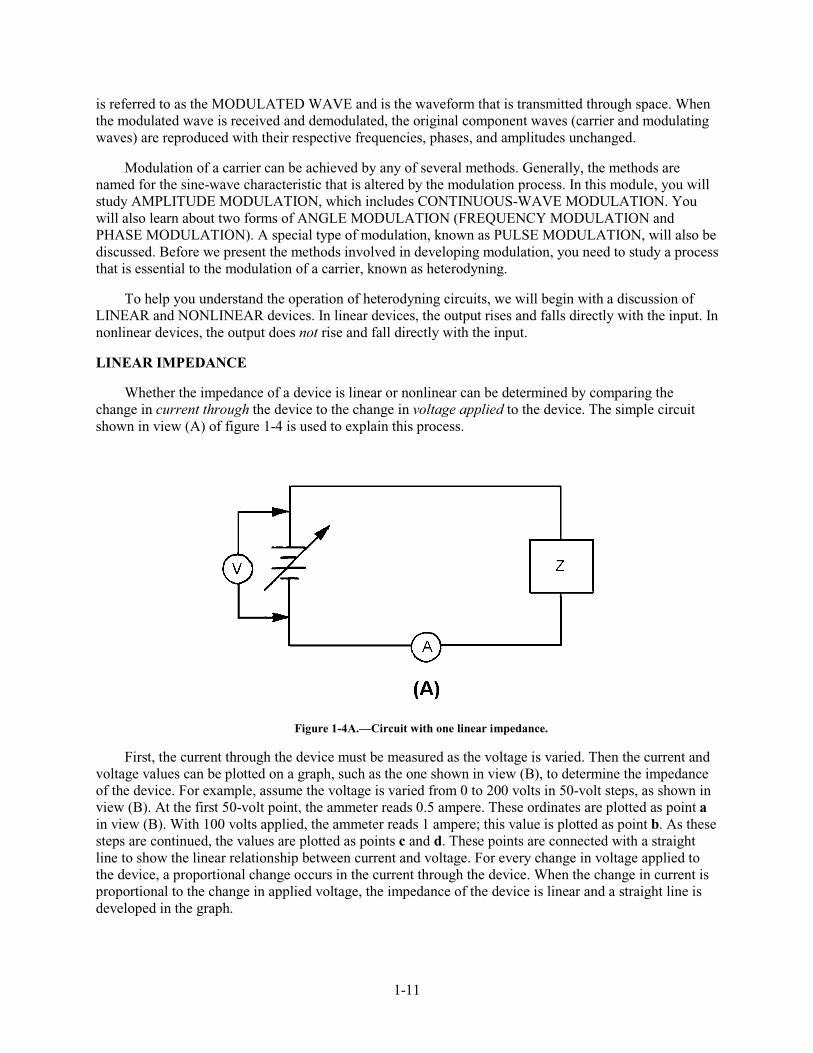
Whether the impedance of a device is linear or nonlinear can be determined by comparing the change in current through the device to the change in voltage applied to the device. The simple circuit shown in view (A) of figure 1-4 is used to explain this process.
Figure 1-4A.—Circuit with one linear impedance.
First, the current through the device must be measured as the voltage is varied. Then the current and voltage values can be plotted on a graph, such as the one shown in view (B), to determine the impedance of the device. For example, assume the voltage is varied from 0 to 200 volts in 50-volt steps, as shown in view (B). At the first 50-volt point, the ammeter reads 0.5 ampere. These ordinates are plotted as point a in view (B). With 100 volts applied, the ammeter reads 1 ampere; this value is plotted as point b. As these steps are continued, the values are plotted as points c and d. These points are connected with a straight line to show the linear relationship between current and voltage. For every change in voltage applied to the device, a proportional change occurs in the current through the device. When the change in current is proportional to the change in applied voltage, the impedance of the device is linear and a straight line is developed in the graph.
1-12
Figure 1-4B.—Circuit with one linear impedance.
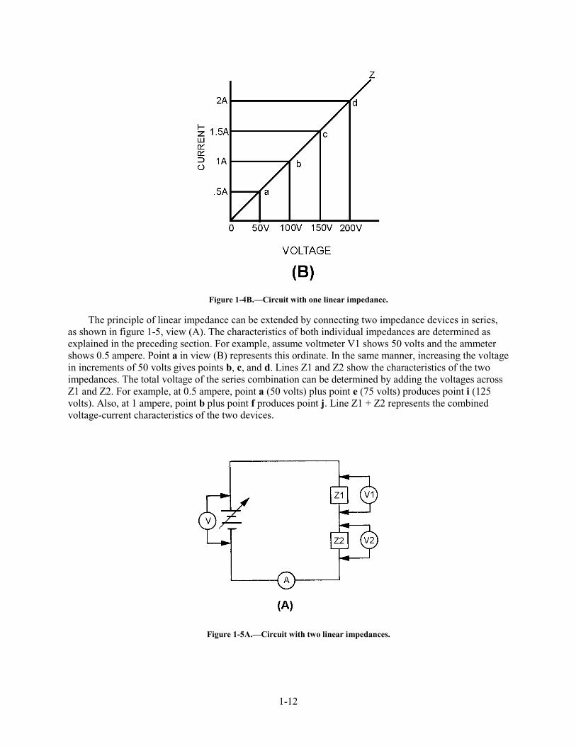
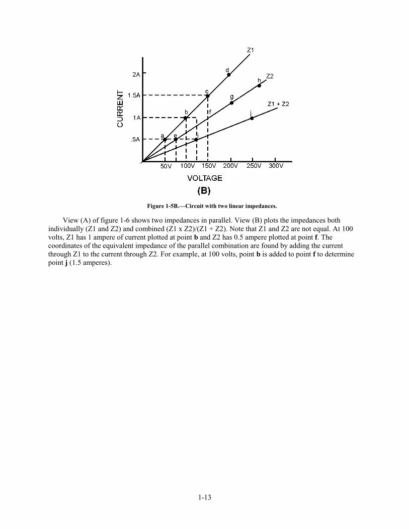
The principle of linear impedance can be extended by connecting two impedance devices in series, as shown in figure 1-5, view (A). The characteristics of both individual impedances are determined as explained in the preceding section. For example, assume voltmeter V1 shows 50 volts and the ammeter shows 0.5 ampere. Point a in view (B) represents this ordinate. In the same manner, increasing the voltage in increments of 50 volts gives points b, c, and d. Lines Z1 and Z2 show the characteristics of the two impedances. The total voltage of the series combination can be determined by adding the voltages across Z1 and Z2. For example, at 0.5 ampere, point a (50 volts) plus point e (75 volts) produces point i (125 volts). Also, at 1 ampere, point b plus point f produces point j. Line Z1 + Z2 represents the combined voltage-current characteristics of the two devices.
Figure 1-5A.—Circuit with two linear impedances.
1-13
Figure 1-5B.—Circuit with two linear impedances.
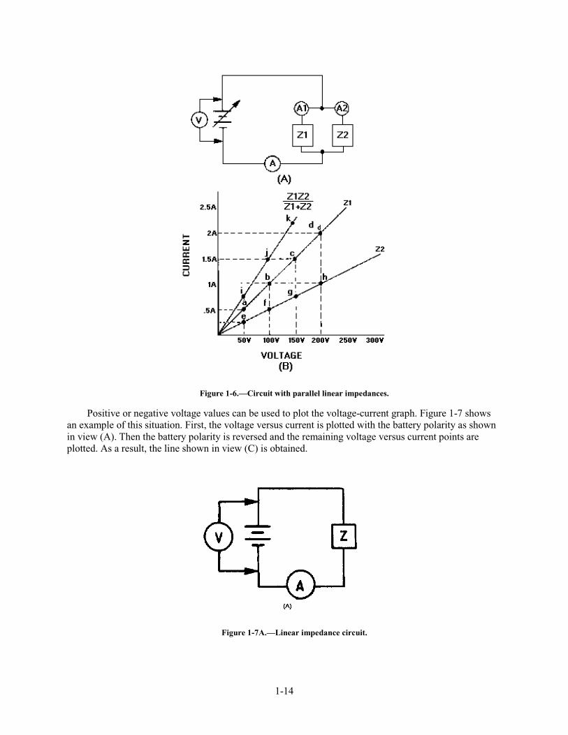
View (A) of figure 1-6 shows two impedances in parallel. View (B) plots the impedances both individually (Z1 and Z2) and combined (Z1 x Z2)/(Z1 + Z2). Note that Z1 and Z2 are not equal. At 100 volts, Z1 has 1 ampere of current plotted at point b and Z2 has 0.5 ampere plotted at point f. The coordinates of the equivalent impedance of the parallel combination are found by adding the current through Z1 to the current through Z2. For example, at 100 volts, point b is added to point f to determine point j (1.5 amperes).
1-14
Figure 1-6.—Circuit with parallel linear impedances.
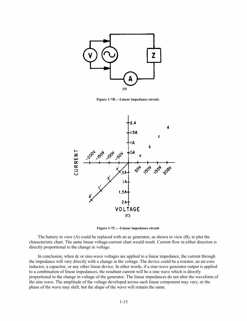
Positive or negative voltage values can be used to plot the voltage-current graph. Figure 1-7 shows an example of this situation. First, the voltage versus current is plotted with the battery polarity as shown in view (A). Then the battery polarity is reversed and the remaining voltage versus current points are plotted. As a result, the line shown in view (C) is obtained.
Figure 1-7A.—Linear impedance circuit.
1-15
Figure 1-7B.—Linear impedance circuit.
Figure 1-7C.—Linear impedance circuit
The battery in view (A) could be replaced with an ac generator, as shown in view (B), to plot the characteristic chart. The same linear voltage-current chart would result. Current flow in either direction is directly proportional to the change in voltage.
In conclusion, when dc or sine-wave voltages are applied to a linear impedance, the current through the impedance will vary directly with a change in the voltage. The device could be a resistor, an air-core inductor, a capacitor, or any other linear device. In other words, if a sine-wave generator output is applied to a combination of linear impedances, the resultant current will be a sine wave which is directly proportional to the change in voltage of the generator. The linear impedances do not alter the waveform of the sine wave. The amplitude of the voltage developed across each linear component may vary, or the phase of the wave may shift, but the shape of the wave will remain the same.
1-16
NONLINEAR IMPEDANCE
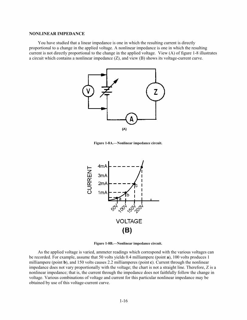
You have studied that a linear impedance is one in which the resulting current is directly proportional to a change in the applied voltage. A nonlinear impedance is one in which the resulting current is not directly proportional to the change in the applied voltage. View (A) of figure 1-8 illustrates a circuit which contains a nonlinear impedance (Z), and view (B) shows its voltage-current curve.
Figure 1-8A.—Nonlinear impedance circuit.
Figure 1-8B.—Nonlinear impedance circuit.
As the applied voltage is varied, ammeter readings which correspond with the various voltages can be recorded. For example, assume that 50 volts yields 0.4 milliampere (point a), 100 volts produces 1 milliampere (point b), and 150 volts causes 2.2 milliamperes (point c). Current through the nonlinear impedance does not vary proportionally with the voltage; the chart is not a straight line. Therefore, Z is a nonlinear impedance; that is, the current through the impedance does not faithfully follow the change in voltage. Various combinations of voltage and current for this particular nonlinear impedance may be obtained by use of this voltage-current curve.
1-17
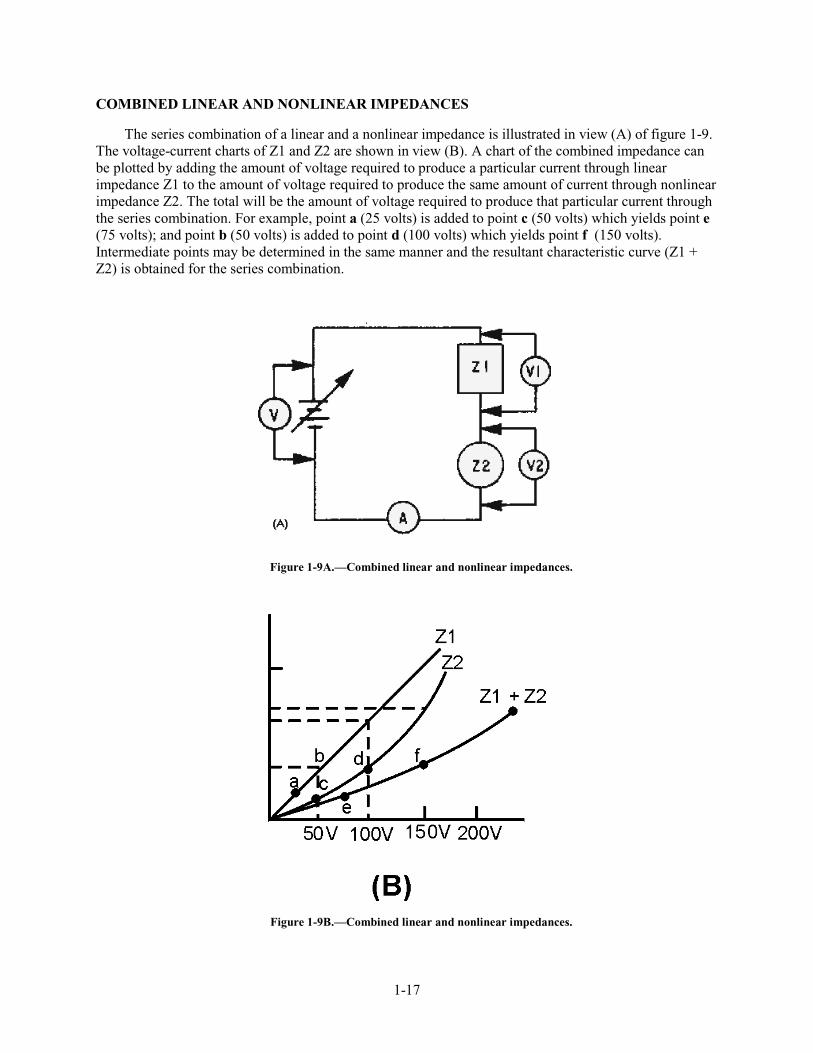
COMBINED LINEAR AND NONLINEAR IMPEDANCES
The series combination of a linear and a nonlinear impedance is illustrated in view (A) of figure 1-9. The voltage-current charts of Z1 and Z2 are shown in view (B). A chart of the combined impedance can be plotted by adding the amount of voltage required to produce a particular current through linear impedance Z1 to the amount of voltage required to produce the same amount of current through nonlinear impedance Z2. The total will be the amount of voltage required to produce that particular current through the series combination. For example, point a (25 volts) is added to point c (50 volts) which yields point e (75 volts); and point b (50 volts) is added to point d (100 volts) which yields point f (150 volts). Intermediate points may be determined in the same manner and the resultant characteristic curve (Z1 + Z2) is obtained for the series combination.
Figure 1-9A.—Combined linear and nonlinear impedances.
Figure 1-9B.—Combined linear and nonlinear impedances.
1-18
You should see from this graphic analysis that when a linear impedance is combined with a nonlinear impedance, the resulting characteristic curve is nonlinear. Some examples of nonlinear impedances are crystal diodes, transistors, iron-core transformers, and electron tubes.
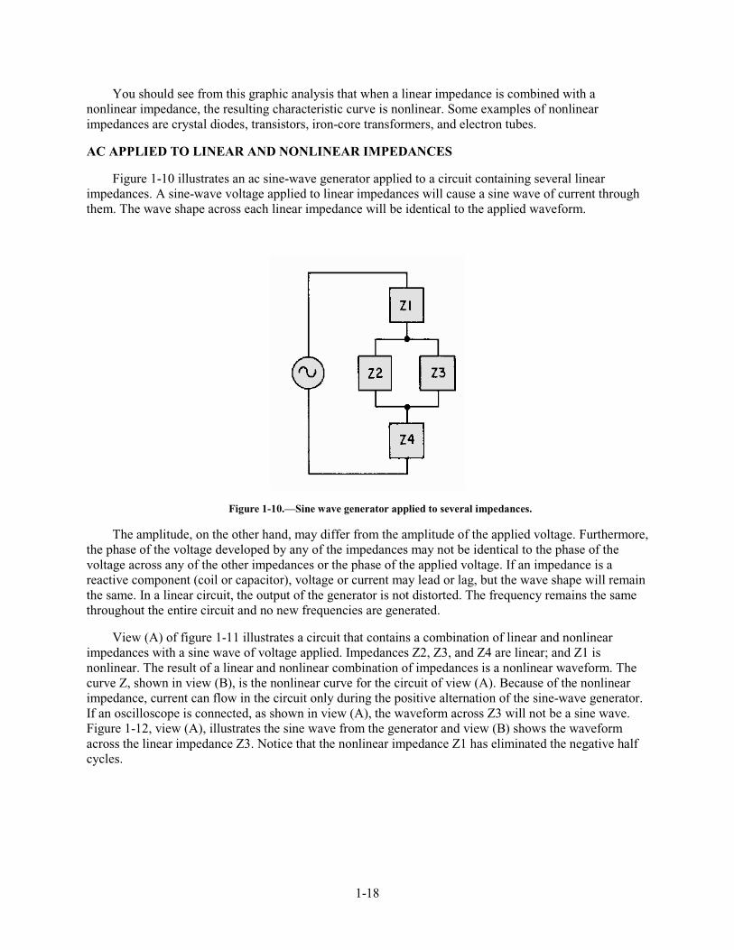
AC APPLIED TO LINEAR AND NONLINEAR IMPEDANCES
Figure 1-10 illustrates an ac sine-wave generator applied to a circuit containing several linear impedances. A sine-wave voltage applied to linear impedances will cause a sine wave of current through them. The wave shape across each linear impedance will be identical to the applied waveform.
Figure 1-10.—Sine wave generator applied to several impedances.
The amplitude, on the other hand, may differ from the amplitude of the applied voltage. Furthermore, the phase of the voltage developed by any of the impedances may not be identical to the phase of the voltage across any of the other impedances or the phase of the applied voltage. If an impedance is a reactive component (coil or capacitor), voltage or current may lead or lag, but the wave shape will remain the same. In a linear circuit, the output of the generator is not distorted. The frequency remains the same throughout the entire circuit and no new frequencies are generated.
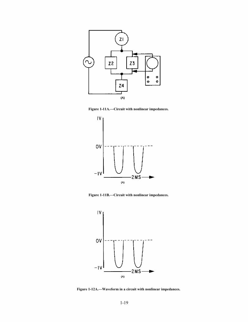
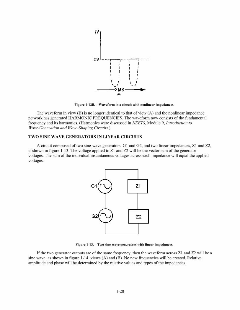
View (A) of figure 1-11 illustrates a circuit that contains a combination of linear and nonlinear impedances with a sine wave of voltage applied. Impedances Z2, Z3, and Z4 are linear; and Z1 is nonlinear. The result of a linear and nonlinear combination of impedances is a nonlinear waveform. The curve Z, shown in view (B), is the nonlinear curve for the circuit of view (A). Because of the nonlinear impedance, current can flow in the circuit only during the positive alternation of the sine-wave generator. If an oscilloscope is connected, as shown in view (A), the waveform across Z3 will not be a sine wave. Figure 1-12, view (A), illustrates the sine wave from the generator and view (B) shows the waveform across the linear impedance Z3. Notice that the nonlinear impedance Z1 has eliminated the negative half cycles.
1-19
Figure 1-11A.—Circuit with nonlinear impedances.
Figure 1-11B.—Circuit with nonlinear impedances.
Figure 1-12A.—Waveform in a circuit with nonlinear impedances.
1-20
Figure 1-12B.—Waveform in a circuit with nonlinear impedances.
The waveform in view (B) is no longer identical to that of view (A) and the nonlinear impedance network has generated HARMONIC FREQUENCIES. The waveform now consists of the fundamental frequency and its harmonics. (Harmonics were discussed in NEETS, Module 9, Introduction to Wave-Generation and Wave-Shaping Circuits.)
TWO SINE WAVE GENERATORS IN LINEAR CIRCUITS
A circuit composed of two sine-wave generators, G1 and G2, and two linear impedances, Z1 and Z2, is shown in figure 1-13. The voltage applied to Z1 and Z2 will be the vector sum of the generator voltages. The sum of the individual instantaneous voltages across each impedance will equal the applied voltages.
Figure 1-13.—Two sine-wave generators with linear impedances.
If the two generator outputs are of the same frequency, then the waveform across Z1 and Z2 will be a sine wave, as shown in figure 1-14, views (A) and (B). No new frequencies will be created. Relative amplitude and phase will be determined by the relative values and types of the impedances.

1-21
Figure 1-14A.—Waveforms across two nonlinear impedances.
Figure 1-14B.—Waveforms across two nonlinear impedances.
If the two sine wave generators are of different frequencies, then the sum of the instantaneous values will appear as a complex wave across the impedances, as shown in figure 1-15, views (A) and (B). To determine the wave shape across each individual impedance, assume only one generator is connected at a
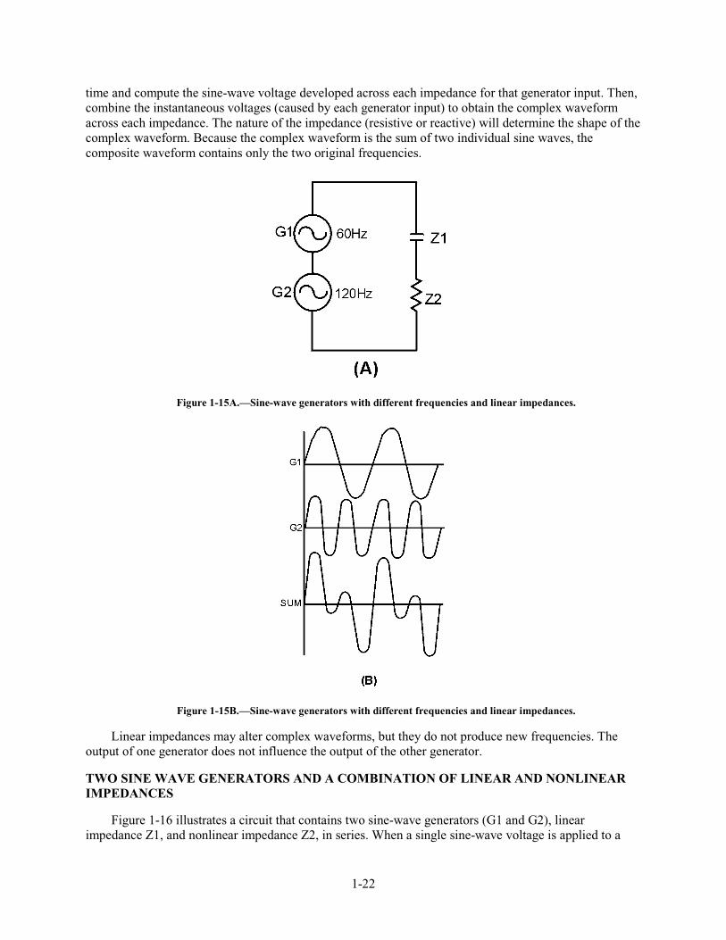
1-22
time and compute the sine-wave voltage developed across each impedance for that generator input. Then, combine the instantaneous voltages (caused by each generator input) to obtain the complex waveform across each impedance. The nature of the impedance (resistive or reactive) will determine the shape of the complex waveform. Because the complex waveform is the sum of two individual sine waves, the composite waveform contains only the two original frequencies.
Figure 1-15A.—Sine-wave generators with different frequencies and linear impedances.
Figure 1-15B.—Sine-wave generators with different frequencies and linear impedances.
Linear impedances may alter complex waveforms, but they do not produce new frequencies. The output of one generator does not influence the output of the other generator.
TWO SINE WAVE GENERATORS AND A COMBINATION OF LINEAR AND NONLINEAR IMPEDANCES
Figure 1-16 illustrates a circuit that contains two sine-wave generators (G1 and G2), linear impedance Z1, and nonlinear impedance Z2, in series. When a single sine-wave voltage is applied to a
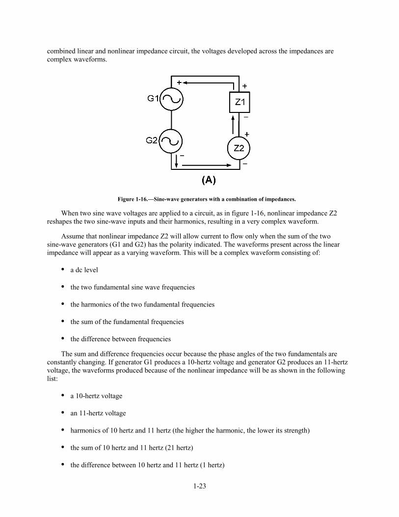
1-23
combined linear and nonlinear impedance circuit, the voltages developed across the impedances are complex waveforms.
Figure 1-16.—Sine-wave generators with a combination of impedances.
When two sine wave voltages are applied to a circuit, as in figure 1-16, nonlinear impedance Z2 reshapes the two sine-wave inputs and their harmonics, resulting in a very complex waveform.
Assume that nonlinear impedance Z2 will allow current to flow only when the sum of the two sine-wave generators (G1 and G2) has the polarity indicated. The waveforms present across the linear impedance will appear as a varying waveform. This will be a complex waveform consisting of:
• a dc level
• the two fundamental sine wave frequencies
• the harmonics of the two fundamental frequencies
• the sum of the fundamental frequencies
• the difference between frequencies
The sum and difference frequencies occur because the phase angles of the two fundamentals are constantly changing. If generator G1 produces a 10-hertz voltage and generator G2 produces an 11-hertz voltage, the waveforms produced because of the nonlinear impedance will be as shown in the following list:
• a 10-hertz voltage
• an 11-hertz voltage
• harmonics of 10 hertz and 11 hertz (the higher the harmonic, the lower its strength)
• the sum of 10 hertz and 11 hertz (21 hertz)
• the difference between 10 hertz and 11 hertz (1 hertz)
1-24
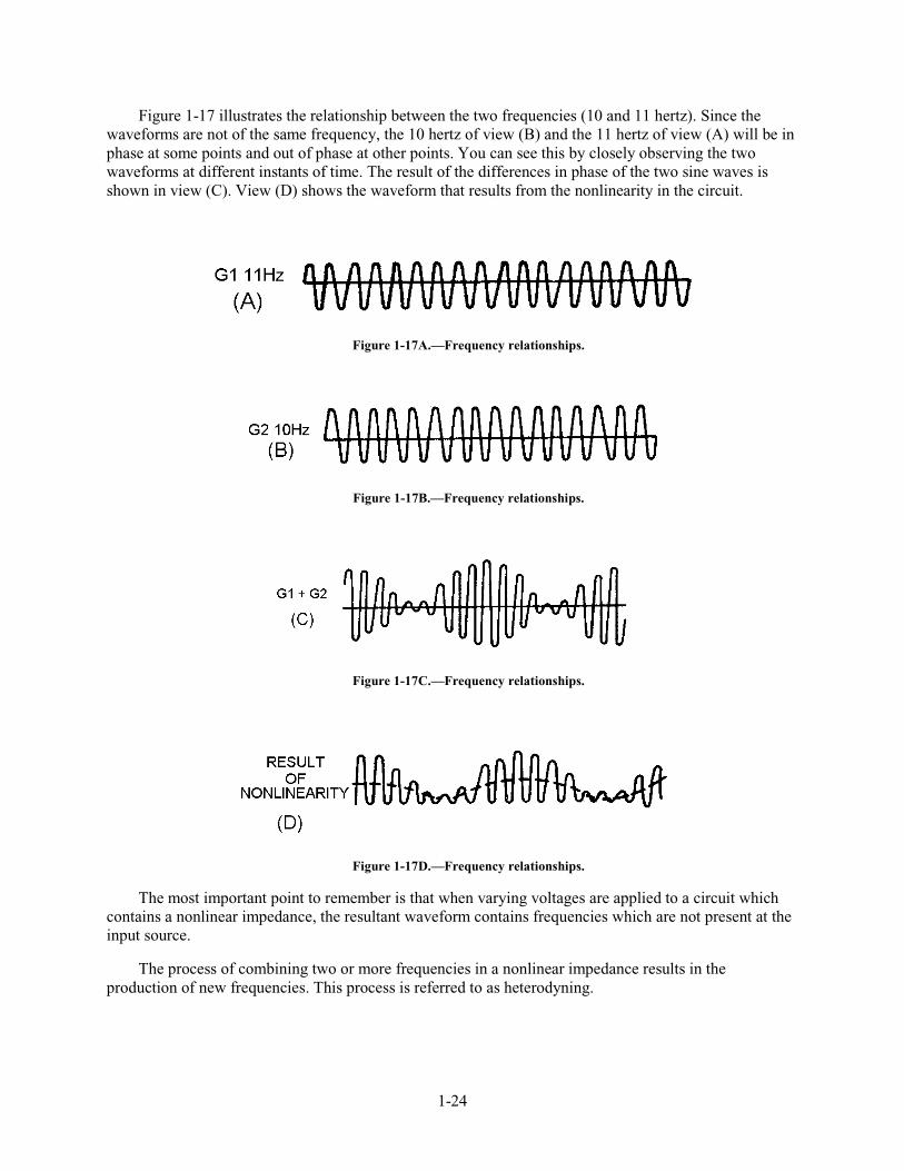
Figure 1-17 illustrates the relationship between the two frequencies (10 and 11 hertz). Since the waveforms are not of the same frequency, the 10 hertz of view (B) and the 11 hertz of view (A) will be in phase at some points and out of phase at other points. You can see this by closely observing the two waveforms at different instants of time. The result of the differences in phase of the two sine waves is shown in view (C). View (D) shows the waveform that results from the nonlinearity in the circuit.
Figure 1-17A.—Frequency relationships.
Figure 1-17B.—Frequency relationships.
Figure 1-17C.—Frequency relationships.
Figure 1-17D.—Frequency relationships.
The most important point to remember is that when varying voltages are applied to a circuit which contains a nonlinear impedance, the resultant waveform contains frequencies which are not present at the input source.
The process of combining two or more frequencies in a nonlinear impedance results in the production of new frequencies. This process is referred to as heterodyning.
1-25
SPECTRUM ANALYSIS
The heterodyning process can be analyzed by using SPECTRUM ANALYSIS (the display of electromagnetic energy arranged according to wavelength or frequency). As shown in figure 1-18, spectrum analysis is an effective way of viewing the energy in electronic circuits. It clearly shows the relationships between the two fundamental frequencies (10 and 11 hertz) and their sum (21 hertz) and difference (1 hertz) frequencies. It also allows you to view the BANDWIDTH (the amount of the frequency spectrum that signals occupy) of the signal you are studying.
Figure 1-18.—Spectrum analysis of heterodyned signal.
TYPICAL HETERODYNING CIRCUIT
Two conditions must be met in a circuit for heterodyning to occur. First, at least two different frequencies must be applied to the circuit. Second, these signals must be applied to a nonlinear impedance. These two conditions will result in new frequencies (sum and difference) being produced. Any one of the frequencies can be selected by placing a frequency-selective device (such as a tuned tank circuit) in series with the nonlinear impedance in the circuit.
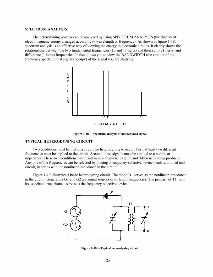
Figure 1-19 illustrates a basic heterodyning circuit. The diode D1 serves as the nonlinear impedance in the circuit. Generators G1 and G2 are signal sources of different frequencies. The primary of T1, with its associated capacitance, serves as the frequency-selective device.
Figure 1-19.—Typical heterodyning circuit.
1-26
The principles of this circuit are similar to those of the block diagram circuit of figure 1-16. Notice in figure 1-19 that the two generators are connected in series. Therefore, the resultant waveform of their combined frequencies will determine when the cathode of D1 will be negative with respect to the anode, thereby controlling the conduction of the diode. The new frequencies that are generated by applying these signals to nonlinear impedance D1 are the sum and difference of the two original frequencies. The frequency-selective device T1 may be tuned to whichever frequency is desired for use in later circuit stages. Heterodyning action takes place, intentionally or not, whenever these conditions exist. Heterodyning (MIXING) circuits are found in most electronic transmitters and receivers. These transmitter and receiver circuits will be explained in detail later in this module.
Q-14. Define the heterodyne principle.
Q-15. What is a nonlinear impedance?
Q-16. What is spectrum analysis?
Q-17. What two conditions are necessary for heterodyning to take place?
AMPLITUDE-MODULATED SYSTEMS
Amplitude modulation refers to any method of varying the amplitude of an electromagnetic carrier frequency in accordance with the intelligence to be transmitted by the carrier. The CARRIER frequency is a radio-frequency wave suitable for modulation by the intelligence to be transmitted. One form of this method of modulation is simply to interrupt the carrier in accordance with a prearranged code.
CONTINUOUS WAVE (CW)
The "on-off" KEYING of a continuous wave (cw) carrier frequency was the principal method of modulating a carrier in the early days of electrical communications. The intervals of time when a carrier either was present or absent conveyed the desired intelligence. This is still used in modern communications. When applied to a continuously oscillating radio-frequency source, on-off keying is referred to as cw signaling. This type of communication is sometimes referred to as an interrupted continuous wave (icw).
Development
The use of a cw transmitter can be very simple. All that is required for the transmitter to work properly is a device to generate the oscillations, a method of keying the oscillations on and off, and an antenna to radiate the energy. Continuous wave was the first type of modulation used. It is still extensively used for long-range communications. When Marconi and others were attempting the transfer of intelligence between two points, without reliance on a conducting path, they employed the use of a practical coding system known as Morse code. You probably know that Morse code is a system of on-off keying developed for telegraph that is capable of passing intelligence over wire at an acceptable rate. Morse code consists only of periods of signal and no-signal.
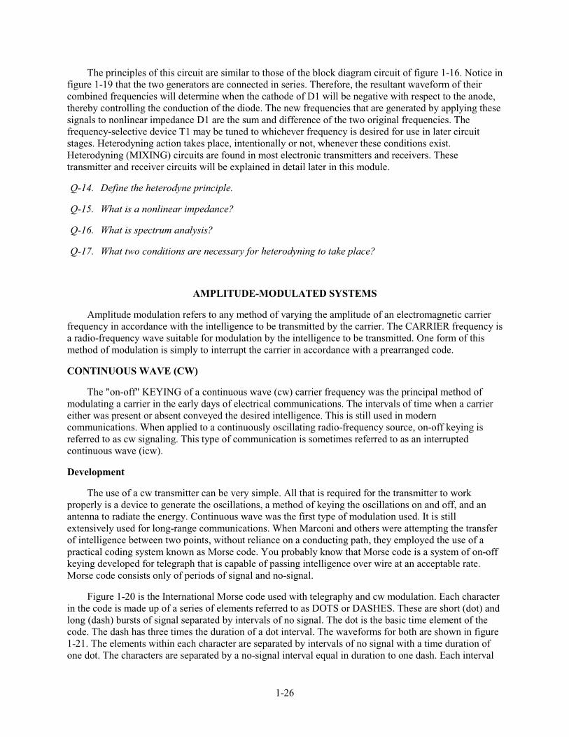
Figure 1-20 is the International Morse code used with telegraphy and cw modulation. Each character in the code is made up of a series of elements referred to as DOTS or DASHES. These are short (dot) and long (dash) bursts of signal separated by intervals of no signal. The dot is the basic time element of the code. The dash has three times the duration of a dot interval. The waveforms for both are shown in figure 1-21. The elements within each character are separated by intervals of no signal with a time duration of one dot. The characters are separated by a no-signal interval equal in duration to one dash. Each interval

1-27
during which signal is present is called the MARKING interval, and the period of no signal is called the SPACING interval. Figure 1-22 shows the relationships between the rf carrier view (A), the on-off keying waveform view (B), and the resultant carrier wave view (C).
Figure 1-20.—International Morse code.
Figure 1-21.—Dot and dash in radiotelegraph code.
1-28
Figure 1-22A.—Essential elements of ON-OFF keying.
Figure 1-22B.—Essential elements of ON-OFF keying.
Figure 1-22C.—Essential elements of ON-OFF keying.
1-29
Keying Methods
Keying a transmitter causes an rf signal to be radiated only when the key contacts are closed. When the key contacts are open, the transmitter does not radiate energy. Keying is accomplished in either the oscillator or amplifier stage of a transmitter. A number of different keying systems are used in Navy transmitters.
In most Navy transmitters, the hand telegraph key is at a low-voltage potential with respect to ground. A keying bar is usually grounded to protect the operator. Generally, a keying relay, with its contacts in the center-tap lead of the filament transformer, is used to key the equipment. Because one or more stages use the same filament transformer, these stages are also keyed. A class C final amplifier, when operated with fixed bias, is usually not keyed. This is because no output occurs when no excitation is applied in class C operation. Keying the final amplifier along with the other stages is not necessary in this case.
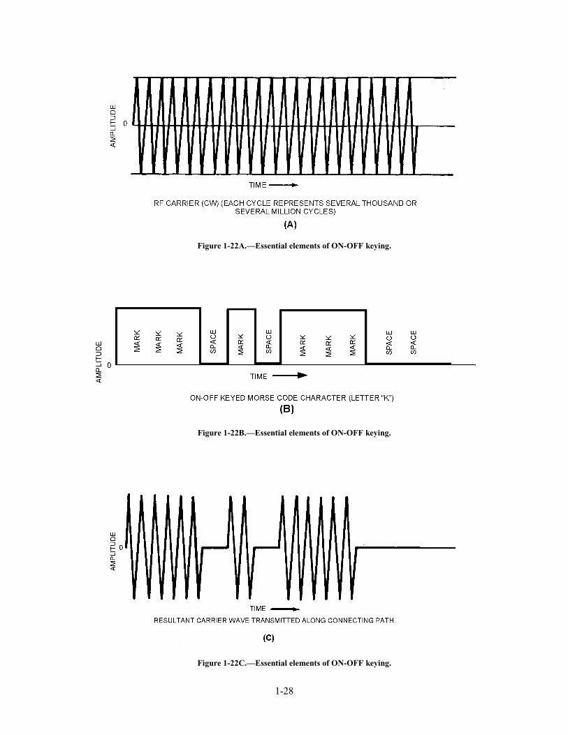
OSCILLATOR KEYING.—Two methods of OSCILLATOR KEYING are shown in figure 1-23. In view (A) the grid circuit is closed at all times. The key (K) opens and closes the negative side of the plate circuit. This system is called PLATE KEYING. When the key is open, no plate current can flow and the circuit does not oscillate. In view (B), the cathode circuit is open when the key is open and neither grid current nor plate current can flow. Both circuits are closed when the key is closed. This system is called CATHODE KEYING. Although the circuits of figure 1-23 may be used to key amplifiers, other keying methods are generally employed because of the high values of plate current and voltage encountered.
Figure 1-23A.—Oscillator keying.
Figure 1-23B.—Oscillator keying.
1-30
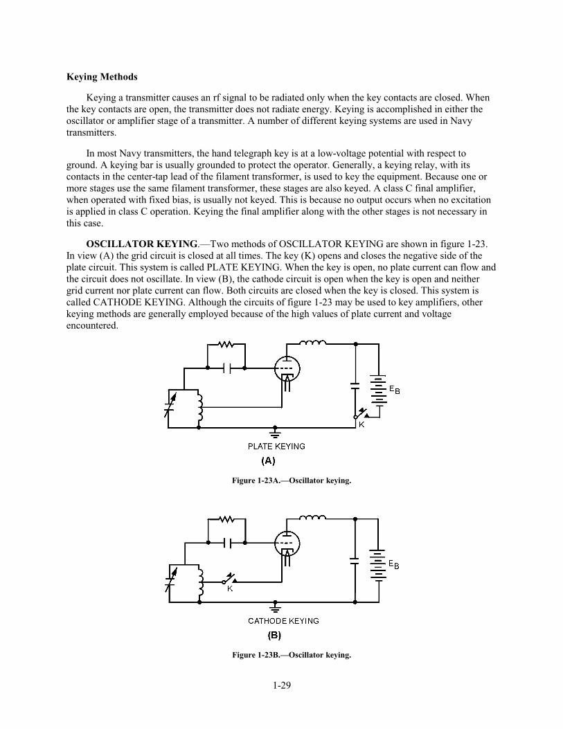
BLOCKED-GRID KEYING.—Two methods of BLOCKED-GRID KEYING are shown in figure 1-24. The key in view (A) shorts cathode resistor R1 allowing normal plate current to flow. With the key open, reduced plate current flows up through resistor R1 making the end connected to grid resistor Rg negative. If R1 has a high enough value, the bias developed is sufficient to cause cutoff of plate current. Depressing the key short-circuits R1. This increases the bias above cutoff and allows the normal flow of plate current. Grid resistor Rg is the usual grid-leak resistor for normal biasing.
Figure 1-24A.—Blocked-grid keying.
Figure 1-24B.—Blocked-grid keying.
The blocked-grid keying method in view (B) affords a complete cutoff of plate current. It is one of the best methods for keying amplifier stages in transmitters. In the voltage divider with the key open, two-thirds of 1,000 volts, or 667 volts, is developed across the 200-kilohm resistor; one-third of 1,000 volts, or 333 volts, is developed across the 100-kilohm resistor. The grid bias is the sum of 100 volts and 333 volts, or 433 volts. This sum is below cutoff and no plate current flows. The plate voltage is 667 volts. With the key closed, the 200-kilohm resistor drops 1,000 volts. The plate voltage becomes 1,000 volts at the same time the grid bias becomes 100 volts. Grid bias is reduced enough so that the triode amplifier will conduct only on the peaks of the drive signal.
1-31
When greater frequency stability is required, the oscillator should not be keyed, but should remain in continuous operation; other transmitter circuits may be keyed. This procedure keeps the oscillator tube at a normal operating temperature and offers less chance for frequency variations to occur each time the key is closed.
KEYING RELAYS.—In transmitters using a crystal-controlled oscillator, the keying is almost always in a circuit stage following the oscillator. In large transmitters (75 watts or higher), the ordinary hand key cannot accommodate the plate current without excessive arcing.
WARNING
BECAUSE OF THE HIGH PLATE POTENTIALS USED, OPERATING A HAND KEY IN THE PLATE CIRCUIT IS DANGEROUS. A SLIGHT SLIP OF THE HAND BELOW THE KEY KNOB COULD RESULT IN SEVERE SHOCK OR, IN THE CASE OF DEFECTIVE RF PLATE CHOKES, A SEVERE RF BURN.
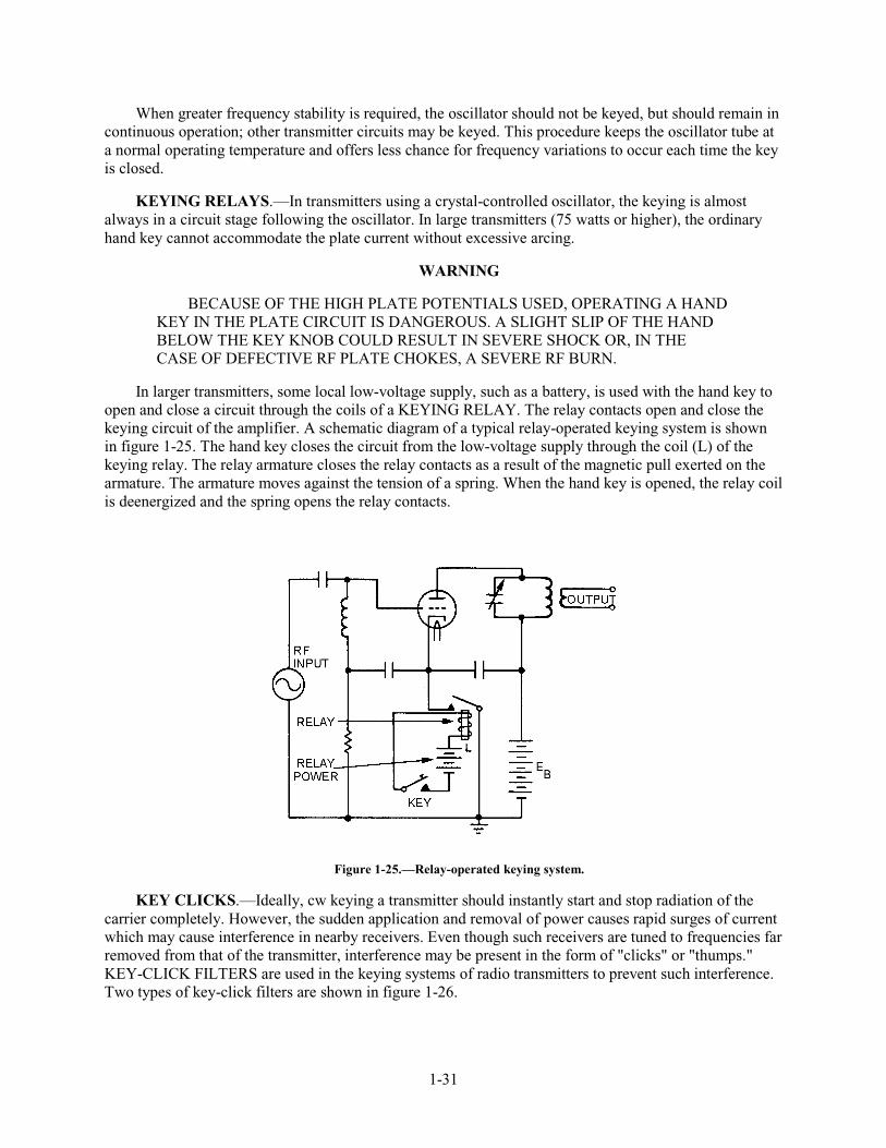
In larger transmitters, some local low-voltage supply, such as a battery, is used with the hand key to open and close a circuit through the coils of a KEYING RELAY. The relay contacts open and close the keying circuit of the amplifier. A schematic diagram of a typical relay-operated keying system is shown in figure 1-25. The hand key closes the circuit from the low-voltage supply through the coil (L) of the keying relay. The relay armature closes the relay contacts as a result of the magnetic pull exerted on the armature. The armature moves against the tension of a spring. When the hand key is opened, the relay coil is deenergized and the spring opens the relay contacts.
Figure 1-25.—Relay-operated keying system.
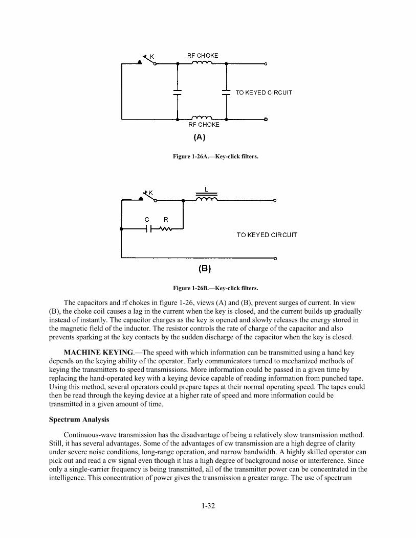
KEY CLICKS.—Ideally, cw keying a transmitter should instantly start and stop radiation of the carrier completely. However, the sudden application and removal of power causes rapid surges of current which may cause interference in nearby receivers. Even though such receivers are tuned to frequencies far removed from that of the transmitter, interference may be present in the form of "clicks" or "thumps." KEY-CLICK FILTERS are used in the keying systems of radio transmitters to prevent such interference. Two types of key-click filters are shown in figure 1-26.
1-32
Figure 1-26A.—Key-click filters.
Figure 1-26B.—Key-click filters.
The capacitors and rf chokes in figure 1-26, views (A) and (B), prevent surges of current. In view (B), the choke coil causes a lag in the current when the key is closed, and the current builds up gradually instead of instantly. The capacitor charges as the key is opened and slowly releases the energy stored in the magnetic field of the inductor. The resistor controls the rate of charge of the capacitor and also prevents sparking at the key contacts by the sudden discharge of the capacitor when the key is closed.
MACHINE KEYING.—The speed with which information can be transmitted using a hand key depends on the keying ability of the operator. Early communicators turned to mechanized methods of keying the transmitters to speed transmissions. More information could be passed in a given time by replacing the hand-operated key with a keying device capable of reading information from punched tape. Using this method, several operators could prepare tapes at their normal operating speed. The tapes could then be read through the keying device at a higher rate of speed and more information could be transmitted in a given amount of time.
Spectrum Analysis
Continuous-wave transmission has the disadvantage of being a relatively slow transmission method. Still, it has several advantages. Some of the advantages of cw transmission are a high degree of clarity under severe noise conditions, long-range operation, and narrow bandwidth. A highly skilled operator can pick out and read a cw signal even though it has a high degree of background noise or interference. Since only a single-carrier frequency is being transmitted, all of the transmitter power can be concentrated in the intelligence. This concentration of power gives the transmission a greater range. The use of spectrum

1-33
analysis (figure 1-27) illustrates the transmitted frequency characteristics of a cw signal. Because the cw signal is a pure sine wave, it occupies only a single frequency in the rf spectrum and the system is relatively simple.
Figure 1-27.—Carrier-wave signal spectrum analysis.
Q-18. What is amplitude modulation?
Q-19. What are the three requirements for cw transmission?
Q-20. Name two methods of oscillator keying.
Q-21. State the method used to increase the speed of keying in a cw transmitter.
Q-22. Name three advantages of cw transmission.
Single-Stage Transmitters
A simple, single-tube cw transmitter can be made by coupling the output of an oscillator directly to an antenna (figure 1-28). The primary purpose of the oscillator is to develop an rf voltage which has a constant frequency and is immune to outside factors which may cause its frequency to shift. The output of this simple transmitter is controlled by placing a telegraph key at point K in series with the voltage supply. Since the plate supply is interrupted when the key is open, the circuit oscillates only as long as the key is closed. Although the transmitter shown uses a Colpitts oscillator, any of the oscillators previously described in NEETS, Module 9, Introduction to Wave-Generation and Wave-Shaping Circuits can be used.
Figure 1-28.—Simple electron-tube transmitter.
1-34
Capacitors C2 and C3 can be GANGED (mechanically linked together) to simplify tuning. Capacitor C1 is used to tune (resonate) the antenna to the transmitter frequency. CA is the effective capacitance existing between the antenna and ground. This antenna-to-ground capacitance is in parallel with the tuning capacitors, C2 and C3. Since the antenna has capacitance, any change in its length or position, such as that caused by swaying of the antenna, changes the value of CA and causes the oscillator to change frequency. Because these frequency changes are undesirable for reliable communications, the multistage transmitter was developed to increase reliability.
Multistage Transmitters
The simple, single-tube transmitter, shown in figure 1-28, is rarely used in practical equipment. Most of the transmitters you will see use a number of tubes or stages. The number used depends on the frequency, power, and application of the equipment. For your study, the following three categories of cw transmitters are discussed: (1) master oscillator power amplifier (mopa) transmitters, (2) multistage, high-power transmitters, (3) high- and very-high frequency transmitters.
The mopa is both an oscillator and a power amplifier. Power-amplifying stages and frequency-multiplying stages must be used to increase power and raise the frequency from those achievable in a mopa. The main difference between many low- and high-power transmitters is in the number of power-amplifying stages that are used. Similarly, the main difference between many high- and very-high frequency transmitters is in the number of frequency-multiplying stages used.
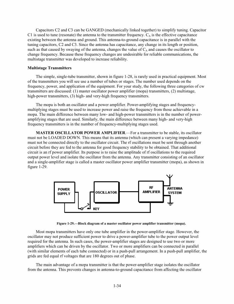
MASTER OSCILLATOR POWER AMPLIFIER.—For a transmitter to be stable, its oscillator must not be LOADED DOWN. This means that its antenna (which can present a varying impedance) must not be connected directly to the oscillator circuit. The rf oscillations must be sent through another circuit before they are fed to the antenna for good frequency stability to be obtained. That additional circuit is an rf power amplifier. Its purpose is to raise the amplitude of rf oscillations to the required output power level and isolate the oscillator from the antenna. Any transmitter consisting of an oscillator and a single-amplifier stage is called a master oscillator power amplifier transmitter (mopa), as shown in figure 1-29.
Figure 1-29.—Block diagram of a master oscillator power amplifier transmitter (mopa).
Most mopa transmitters have only one tube amplifier in the power-amplifier stage. However, the oscillator may not produce sufficient power to drive a power-amplifier tube to the power output level required for the antenna. In such cases, the power-amplifier stages are designed to use two or more amplifiers which can be driven by the oscillator. Two or more amplifiers can be connected in parallel (with similar elements of each tube connected) or in a push-pull arrangement. In a push-pull amplifier, the grids are fed equal rf voltages that are 180 degrees out of phase.
The main advantage of a mopa transmitter is that the power-amplifier stage isolates the oscillator from the antenna. This prevents changes in antenna-to-ground capacitance from affecting the oscillator
1-35
frequency. A second advantage is that the rf power amplifier is operated so that a small change in the voltage applied to its grid circuit will produce a large change in the power developed in its plate circuit.
Rf power amplifiers require that a specific amount of power be fed into the grid circuit. Only in this way can the tube deliver an amplified power output. However, the stable oscillator can produce only limited amounts of power. Therefore, the mopa transmitter is limited in the amount of power it can develop. This is one of the disadvantages of the mopa transmitter. Another disadvantage is that it often is impractical for use at very- and ultra-high frequencies. The reason is that the stability of self-excited oscillators decreases rapidly as the operating frequency increases. Circuit tuning capacitances are small at high frequencies and stray capacitances adversely affect frequency stability.
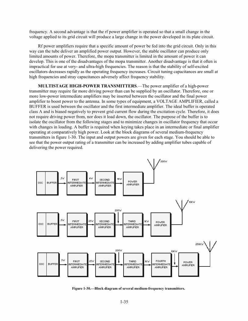
MULTISTAGE HIGH-POWER TRANSMITTERS.—The power amplifier of a high-power transmitter may require far more driving power than can be supplied by an oscillator. Therefore, one or more low-power intermediate amplifiers may be inserted between the oscillator and the final power amplifier to boost power to the antenna. In some types of equipment, a VOLTAGE AMPLIFIER, called a BUFFER is used between the oscillator and the first intermediate amplifier. The ideal buffer is operated class A and is biased negatively to prevent grid current flow during the excitation cycle. Therefore, it does not require driving power from, nor does it load down, the oscillator. The purpose of the buffer is to isolate the oscillator from the following stages and to minimize changes in oscillator frequency that occur with changes in loading. A buffer is required when keying takes place in an intermediate or final amplifier operating at comparatively high power. Look at the block diagrams of several medium-frequency transmitters in figure 1-30. The input and output powers are given for each stage. You should be able to see that the power output rating of a transmitter can be increased by adding amplifier tubes capable of delivering the power required.
Figure 1-30.—Block diagram of several medium-frequency transmitters.

1-36
HF AND VHF TRANSMITTERS.—Oscillators are too unstable for direct frequency control in very- and ultra-high frequency transmitters. Therefore, these transmitters have oscillators operating at comparatively low frequencies, sometimes as low as 1/100 of the output frequency. The oscillator frequency is raised to the required output frequency by passing it through one or more FREQUENCY MULTIPLIERS. Frequency multipliers are special rf power amplifiers which multiply the input frequency. In practice, the MULTIPLICATION FACTOR (number of times the input frequency is multiplied) is seldom larger than five in any one stage. The block diagram of a typical VHF transmitter, designed for continuous tuning between 256 and 288 megahertz, is shown in figure 1-31.
Figure 1-31.—Block diagram of a vhf transmitter.
The stages which multiply the frequency by two are DOUBLERS; those which multiply by four are QUADRUPLERS. The oscillator is tunable from 4 to 4.5 megahertz. The multiplier stages increase the frequency by multiplying successively by 4, 4, 2, and 2, for a total factor of 64. In high-power, high-frequency transmitters, one or more intermediate amplifiers may be used between the last frequency multiplier and the power amplifier.
Q-23. Name a disadvantage of a single-stage cw transmitter.
Q-24. What is the purpose of the power-amplifier stage in a master oscillator power amplifier cw transmitter?
Q-25. What is the purpose of frequency-multiplier stages in a VHF transmitter?
AMPLITUDE MODULATION
The telegraph and radiotelegraph improved man's ability to communicate by allowing speedy passage of information between two distant points. However, it failed to satisfy one of man's other communications needs; that is, the ability to hear and be heard, by voice, at a great distance. In an effort to improve on the telegraph, Alexander Graham Bell developed the principles on which modern communications are built. He developed the modulation of an electric current by complex waveforms, the demodulation of the resulting wave, and recovery of the original waveform. This section will examine the process of varying an electric current in amplitude at an audio frequency.

1-37
Microphones
If an rf carrier is to convey intelligence, some feature of the carrier must be varied in accordance with the information to be transmitted. In the case of speech intelligence, sound waves must be converted to electrical energy.
A MICROPHONE is an energy converter that changes sound energy into electrical energy. A diaphragm in the microphone moves in and out in accordance with the compression and rarefaction of the atmosphere caused by sound waves. The diaphragm is connected to a device that causes current flow in proportion to the instantaneous pressure delivered to it. Many devices can perform this function. The particular device used in a given application depends on the characteristics desired, such as sensitivity, frequency response, impedance matching, power requirements, and ruggedness.
The SENSITIVITY or EFFICIENCY of a microphone is usually expressed in terms of the electrical power level which the microphone delivers to a matched-impedance load compared to the sound level being converted. The sensitivity is rated in dB and must be as high as possible. A high microphone output requires less gain in the amplifiers used with the microphone. This keeps the effects of thermal noise, amplifier hum, and noise pickup at a minimum.
For good quality sound reproduction, the electrical signal from the microphone must correspond in frequency content to the original sound waves. The microphone response should be uniform, or flat, within its frequency range and free from the electrical or mechanical generation of new frequencies.
The impedance of a microphone is important in that it must be matched to the microphone cable and to the amplifier input as well as to the amplifier input load. Exact impedance matching is not always possible, especially in the case where the impedance of the microphone increases with an increase in frequency. A long microphone cable tends to seriously attenuate the high frequencies if the microphone impedance is high. This attenuation is caused by the increased capacitive action of the line at higher frequencies. If the microphone has a low impedance, a lower voltage is developed in the microphone, and more voltage is available at the load. Because many microphone lines used aboard ship are long, low-impedance microphones must be used to preserve a sufficiently high voltage level- over the required frequency range.
The symbol used to represent a microphone in a schematic diagram is shown in figure 1-32. The schematic symbol identifies neither the type of microphone used nor its characteristics.
Figure 1-32.—Microphone schematic symbol.
CARBON MICROPHONE.—Operation of the SINGLE-BUTTON CARBON MICROPHONE figure 1-33, view (A) is based on varying the resistance of a pile of carbon granules located within the microphone. An insulated cup, referred to as the button, holds the loosely piled granules. It is so mounted that it is in constant contact with the thin metal diaphragm. Sound waves striking the diaphragm vary the pressure on the button which varies the pressure on the pile of carbon granules. The dc resistance of the carbon granule pile is varied by this pressure. This varying resistance is in series with a battery and the
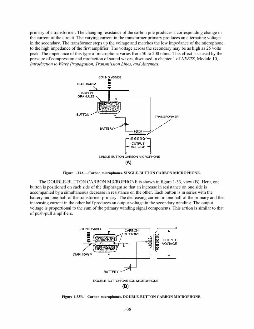
1-38
primary of a transformer. The changing resistance of the carbon pile produces a corresponding change in the current of the circuit. The varying current in the transformer primary produces an alternating voltage in the secondary. The transformer steps up the voltage and matches the low impedance of the microphone to the high impedance of the first amplifier. The voltage across the secondary may be as high as 25 volts peak. The impedance of this type of microphone varies from 50 to 200 ohms. This effect is caused by the pressure of compression and rarefaction of sound waves, discussed in chapter 1 of NEETS, Module 10, Introduction to Wave Propagation, Transmission Lines, and Antennas.
Figure 1-33A.—Carbon microphones. SINGLE-BUTTON CARBON MICROPHONE.
The DOUBLE-BUTTON CARBON MICROPHONE is shown in figure 1-33, view (B). Here, one button is positioned on each side of the diaphragm so that an increase in resistance on one side is accompanied by a simultaneous decrease in resistance on the other. Each button is in series with the battery and one-half of the transformer primary. The decreasing current in one-half of the primary and the increasing current in the other half produces an output voltage in the secondary winding. The output voltage is proportional to the sum of the primary winding signal components. This action is similar to that of push-pull amplifiers.
Figure 1-33B.—Carbon microphones. DOUBLE-BUTTON CARBON MICROPHONE.
1-39
One disadvantage of carbon microphones is that of a constant BACKGROUND HISS (hissing noise) which results from random changes in the resistance between individual carbon granules. Other disadvantages are reduced sensitivity and distortion that may result from the granules packing or sticking together. The carbon microphone also has a limited frequency response. Still another disadvantage is a requirement for an external voltage source.
The disadvantages, however, are offset by advantages that make its use in military applications widespread. It is lightweight, rugged, and can produce an extremely high output.
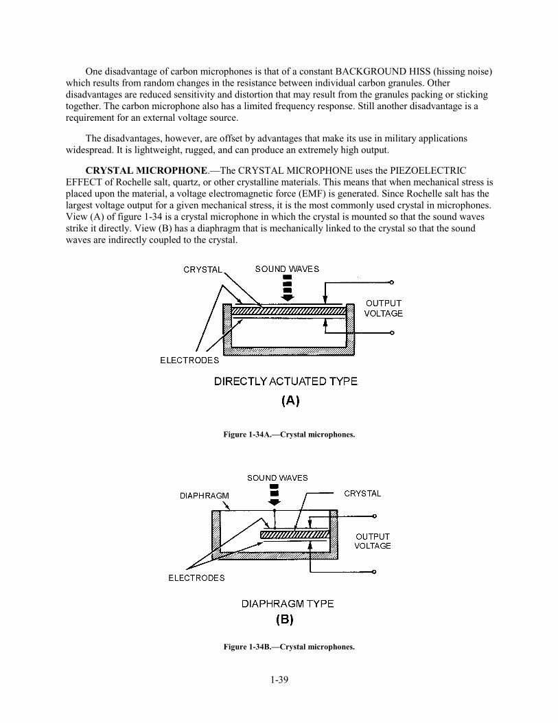
CRYSTAL MICROPHONE.—The CRYSTAL MICROPHONE uses the PIEZOELECTRIC EFFECT of Rochelle salt, quartz, or other crystalline materials. This means that when mechanical stress is placed upon the material, a voltage electromagnetic force (EMF) is generated. Since Rochelle salt has the largest voltage output for a given mechanical stress, it is the most commonly used crystal in microphones. View (A) of figure 1-34 is a crystal microphone in which the crystal is mounted so that the sound waves strike it directly. View (B) has a diaphragm that is mechanically linked to the crystal so that the sound waves are indirectly coupled to the crystal.
Figure 1-34A.—Crystal microphones.
Figure 1-34B.—Crystal microphones.
1-40
A crystal microphone has a high impedance and does not require an external voltage source. It can be connected directly into the input circuit of a high-gain amplifier. However, because its output is low, several stages of high-gain amplification are required. Crystal microphones are delicate and must be handled with care. Exposure to temperatures above 52 degrees Celsius (125 degrees Fahrenheit) may permanently damage the crystal unit. Crystals are also soluble in water and other liquids and must be protected from moisture and excessive humidity.
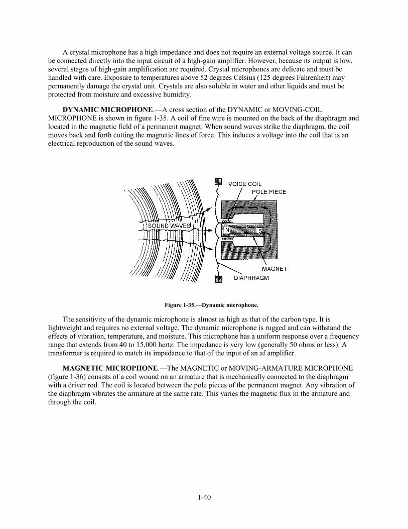
DYNAMIC MICROPHONE.—A cross section of the DYNAMIC or MOVING-COIL MICROPHONE is shown in figure 1-35. A coil of fine wire is mounted on the back of the diaphragm and located in the magnetic field of a permanent magnet. When sound waves strike the diaphragm, the coil moves back and forth cutting the magnetic lines of force. This induces a voltage into the coil that is an electrical reproduction of the sound waves.
Figure 1-35.—Dynamic microphone.
The sensitivity of the dynamic microphone is almost as high as that of the carbon type. It is lightweight and requires no external voltage. The dynamic microphone is rugged and can withstand the effects of vibration, temperature, and moisture. This microphone has a uniform response over a frequency range that extends from 40 to 15,000 hertz. The impedance is very low (generally 50 ohms or less). A transformer is required to match its impedance to that of the input of an af amplifier.
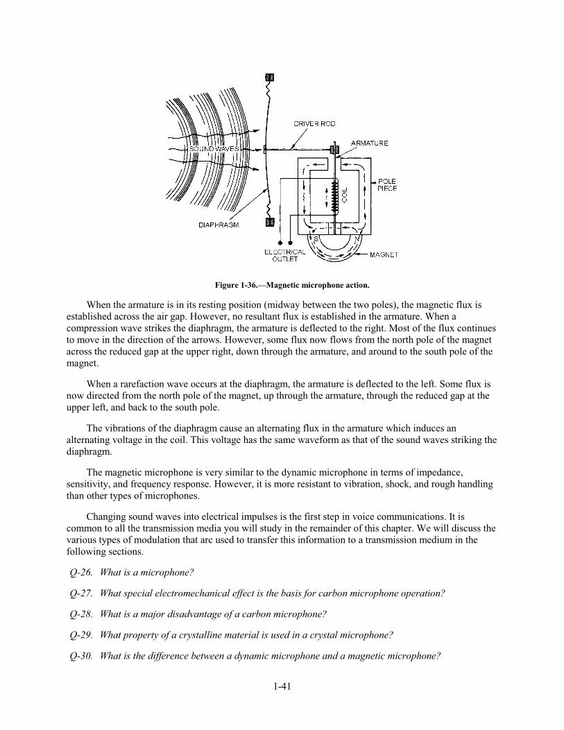
MAGNETIC MICROPHONE.—The MAGNETIC or MOVING-ARMATURE MICROPHONE (figure 1-36) consists of a coil wound on an armature that is mechanically connected to the diaphragm with a driver rod. The coil is located between the pole pieces of the permanent magnet. Any vibration of the diaphragm vibrates the armature at the same rate. This varies the magnetic flux in the armature and through the coil.
1-41
Figure 1-36.—Magnetic microphone action.
When the armature is in its resting position (midway between the two poles), the magnetic flux is established across the air gap. However, no resultant flux is established in the armature. When a compression wave strikes the diaphragm, the armature is deflected to the right. Most of the flux continues to move in the direction of the arrows. However, some flux now flows from the north pole of the magnet across the reduced gap at the upper right, down through the armature, and around to the south pole of the magnet.
When a rarefaction wave occurs at the diaphragm, the armature is deflected to the left. Some flux is now directed from the north pole of the magnet, up through the armature, through the reduced gap at the upper left, and back to the south pole.
The vibrations of the diaphragm cause an alternating flux in the armature which induces an alternating voltage in the coil. This voltage has the same waveform as that of the sound waves striking the diaphragm.
The magnetic microphone is very similar to the dynamic microphone in terms of impedance, sensitivity, and frequency response. However, it is more resistant to vibration, shock, and rough handling than other types of microphones.
Changing sound waves into electrical impulses is the first step in voice communications. It is common to all the transmission media you will study in the remainder of this chapter. We will discuss the various types of modulation that arc used to transfer this information to a transmission medium in the following sections.
Q-26. What is a microphone?
Q-27. What special electromechanical effect is the basis for carbon microphone operation?
Q-28. What is a major disadvantage of a carbon microphone?
Q-29. What property of a crystalline material is used in a crystal microphone?
Q-30. What is the difference between a dynamic microphone and a magnetic microphone?
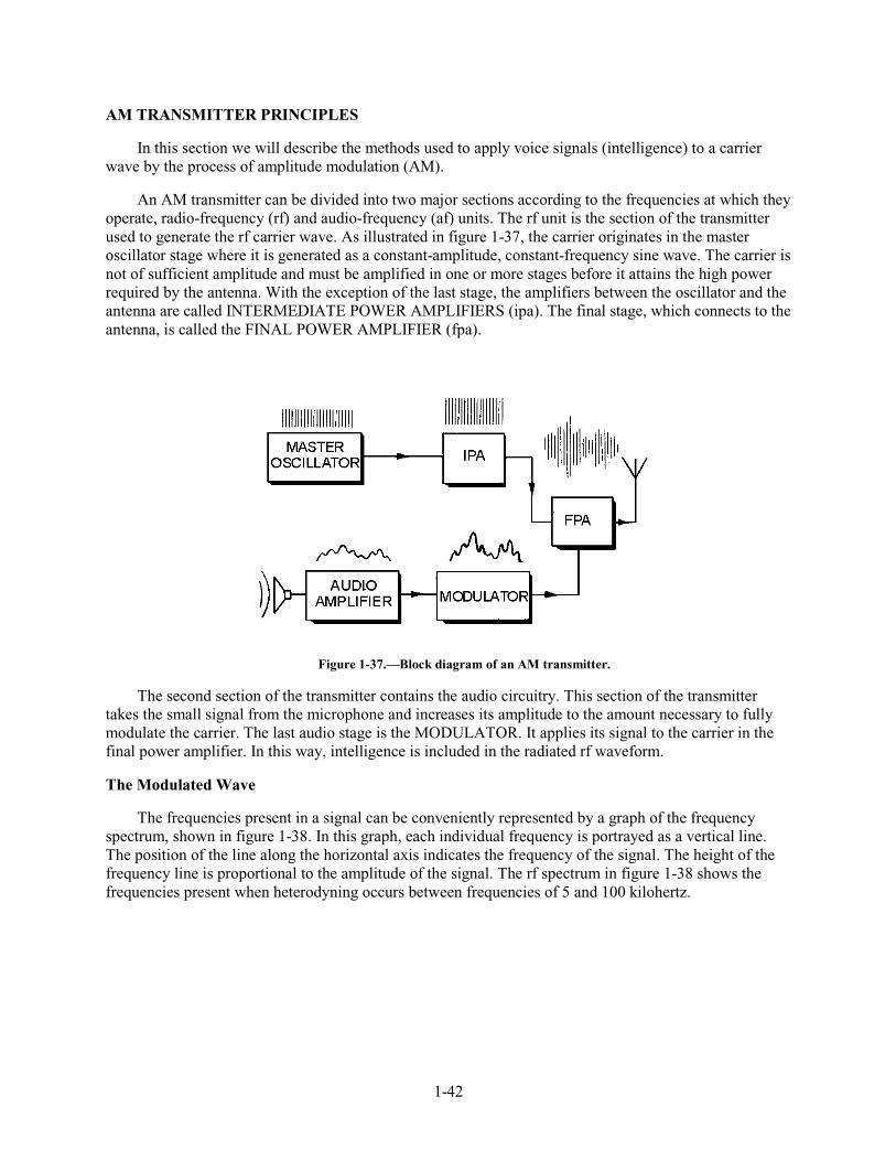
1-42
AM TRANSMITTER PRINCIPLES
In this section we will describe the methods used to apply voice signals (intelligence) to a carrier wave by the process of amplitude modulation (AM).
An AM transmitter can be divided into two major sections according to the frequencies at which they operate, radio-frequency (rf) and audio-frequency (af) units. The rf unit is the section of the transmitter used to generate the rf carrier wave. As illustrated in figure 1-37, the carrier originates in the master oscillator stage where it is generated as a constant-amplitude, constant-frequency sine wave. The carrier is not of sufficient amplitude and must be amplified in one or more stages before it attains the high power required by the antenna. With the exception of the last stage, the amplifiers between the oscillator and the antenna are called INTERMEDIATE POWER AMPLIFIERS (ipa). The final stage, which connects to the antenna, is called the FINAL POWER AMPLIFIER (fpa).
Figure 1-37.—Block diagram of an AM transmitter.
The second section of the transmitter contains the audio circuitry. This section of the transmitter takes the small signal from the microphone and increases its amplitude to the amount necessary to fully modulate the carrier. The last audio stage is the MODULATOR. It applies its signal to the carrier in the final power amplifier. In this way, intelligence is included in the radiated rf waveform.
The Modulated Wave
The frequencies present in a signal can be conveniently represented by a graph of the frequency spectrum, shown in figure 1-38. In this graph, each individual frequency is portrayed as a vertical line. The position of the line along the horizontal axis indicates the frequency of the signal. The height of the frequency line is proportional to the amplitude of the signal. The rf spectrum in figure 1-38 shows the frequencies present when heterodyning occurs between frequencies of 5 and 100 kilohertz.

1-43
Figure 1-38.—Radio-frequency spectrum.
Radiating energy at audio frequencies (discussed earlier in this chapter) is not practical. The heterodyning principle, however, makes possible the conversion of an af signal (intelligence) to an rf signal (with af intelligence) which can be radiated or transmitted through space.
Look again at figure 1-38. The sum and difference frequencies are located very near the rf signal (100 kilohertz), while the audio signal (5 kilohertz) is spaced a considerable distance away. Because of this frequency separation, the audio frequency can be easily removed by filter circuits, leaving just three radio frequencies of 95, 100, and 105 kilohertz. These three radio frequencies are radiated through space to the receiving station. At the receiver, the process is reversed. The frequency of 95 kilohertz, for example, is heterodyned with the frequency of 100 kilohertz and the sum and difference frequencies are again produced. (A similar process occurs between the frequencies of 100 and 105 kilohertz.) Of the resultant frequencies (95, 100, 105, and 5 kilohertz), all are filtered out except the 5 kilohertz difference frequency. This frequency, which is identical to the original 5 kilohertz audio applied at the transmitter, is retained and amplified. Thus, the 5 kilohertz audio tone appears to have been radiated through space from the transmitter to the receiver.
In the process just described, the 100 kilohertz frequency is referred to as the CARRIER FREQUENCY, and the sum and difference frequencies are referred to as SIDE FREQUENCIES. Since the sum frequency appears above the carrier frequency, it is referred to as the UPPER SIDE FREQUENCY. The difference frequency appears below the carrier and is referred to as the LOWER SIDE FREQUENCY.
When a carrier is modulated by voice or music signals, a large number of sum and difference frequencies are produced. All of the sum frequencies above the carrier are spoken of collectively as the UPPER SIDEBAND. All the difference frequencies below the carrier, also considered as a group, are called the LOWER SIDEBAND.
If the carrier and the modulating signal are constant in amplitude, the sum and difference frequencies will also be constant in amplitude. However, when the carrier and sidebands are combined in a single impedance and viewed simultaneously with an oscilloscope, the resultant waveform appears as shown in figure 1-39. This resultant wave is called the MODULATION ENVELOPE. The modulation envelope has the same frequency as the carrier. However, it rises and falls in amplitude with the continual phase shift between the carrier and sidebands. This causes these signals to first aid and then oppose one another. These cyclic variations in the amplitude of the envelope have the same frequency as the audio-modulating
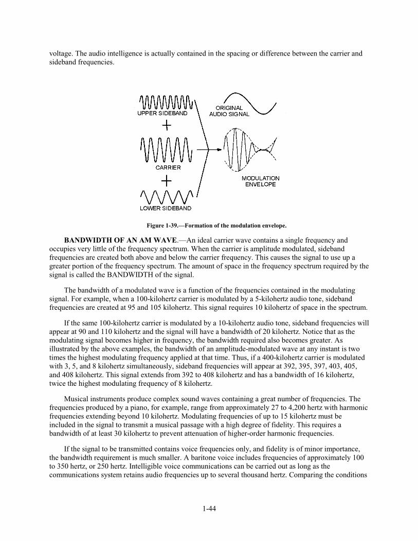
1-44
voltage. The audio intelligence is actually contained in the spacing or difference between the carrier and sideband frequencies.
Figure 1-39.—Formation of the modulation envelope.
BANDWIDTH OF AN AM WAVE.—An ideal carrier wave contains a single frequency and occupies very little of the frequency spectrum. When the carrier is amplitude modulated, sideband frequencies are created both above and below the carrier frequency. This causes the signal to use up a greater portion of the frequency spectrum. The amount of space in the frequency spectrum required by the signal is called the BANDWIDTH of the signal.
The bandwidth of a modulated wave is a function of the frequencies contained in the modulating signal. For example, when a 100-kilohertz carrier is modulated by a 5-kilohertz audio tone, sideband frequencies are created at 95 and 105 kilohertz. This signal requires 10 kilohertz of space in the spectrum.
If the same 100-kilohertz carrier is modulated by a 10-kilohertz audio tone, sideband frequencies will appear at 90 and 110 kilohertz and the signal will have a bandwidth of 20 kilohertz. Notice that as the modulating signal becomes higher in frequency, the bandwidth required also becomes greater. As illustrated by the above examples, the bandwidth of an amplitude-modulated wave at any instant is two times the highest modulating frequency applied at that time. Thus, if a 400-kilohertz carrier is modulated with 3, 5, and 8 kilohertz simultaneously, sideband frequencies will appear at 392, 395, 397, 403, 405, and 408 kilohertz. This signal extends from 392 to 408 kilohertz and has a bandwidth of 16 kilohertz, twice the highest modulating frequency of 8 kilohertz.
Musical instruments produce complex sound waves containing a great number of frequencies. The frequencies produced by a piano, for example, range from approximately 27 to 4,200 hertz with harmonic frequencies extending beyond 10 kilohertz. Modulating frequencies of up to 15 kilohertz must be included in the signal to transmit a musical passage with a high degree of fidelity. This requires a bandwidth of at least 30 kilohertz to prevent attenuation of higher-order harmonic frequencies.
If the signal to be transmitted contains voice frequencies only, and fidelity is of minor importance, the bandwidth requirement is much smaller. A baritone voice includes frequencies of approximately 100 to 350 hertz, or 250 hertz. Intelligible voice communications can be carried out as long as the communications system retains audio frequencies up to several thousand hertz. Comparing the conditions
1-45
for transmitting voice signals with those for transmitting music reveals that much less spectrum space is required for voice communications.
Radio stations in the standard broadcast band are assigned carrier frequencies by the Federal Communications Commission (FCC). When two stations are located near each other, their carriers must be spaced some minimum distance apart in the radio spectrum. Otherwise, the sideband frequencies of one station will interfere with sideband frequencies of the other station. The standard AM broadcast band starts at 535 kilohertz and ends at 1,605 kilohertz. Carrier assignments start at 540 kilohertz and continue in a succession of 10-kilohertz increments until the upper limit of the broadcast band is reached. This adds up to a total of 107 carrier assignments, or CHANNELS, over the entire broadcast band. If stations were assigned to all 107 channels (in a given geographical area), each station would be allotted a channel width of 10 kilohertz. This leaves 5 kilohertz on each side of each carrier for sidebands. Since interference between such closely spaced stations would be nearly impossible to prevent, the FCC avoids assigning adjacent channels to stations in the same area. As a consequence of this policy, one or more vacant channels normally exist between stations in the broadcast band. In the interest of better fidelity, the stations are permitted to use modulating frequencies higher than 5 kilohertz as long as no interference with other stations is produced.
Q-31. What are the two major sections of a typical AM transmitter?
Q-32. When 100 kilohertz and 5 kilohertz are heterodyned, what frequencies are present?
Q-33. What is the upper sideband of an AM transmission?
Q-34. Where is the intelligence in an AM transmission located?
Q-35. What determines the bandwidth of an AM transmission?
ANALYSIS OF AN AM WAVE.—A significant amount of information concerning the basic principles of amplitude modulation can be obtained from a study of the properties of the modulation envelope.
A carrier wave which has been modulated by voice or music signals is accompanied by two sidebands; each sideband contains individual frequencies that vary continuously. Since a wave of this nature is nearly impossible to analyze, you can assume in the following sections that the modulating signal, unless otherwise qualified, is a single-frequency, constant-amplitude sine wave.
PERCENT OF MODULATION IN AN AM WAVE.—The degree of modulation is defined in terms of the maximum permissible amount of modulation. Thus, a fully modulated wave is said to be 100-PERCENT MODULATED. The modulation envelope in figure 1-40, view (A), shows the conditions for 100-percent sine-wave modulation. For this degree of modulation, the peak audio voltage must be equal to the dc supply voltage to the final power amplifier. Under these conditions, the rf output voltage will reach 0 on the negative peak of the modulating signal; on the positive peak, it will rise to twice the amplitude of the unmodulated carrier.
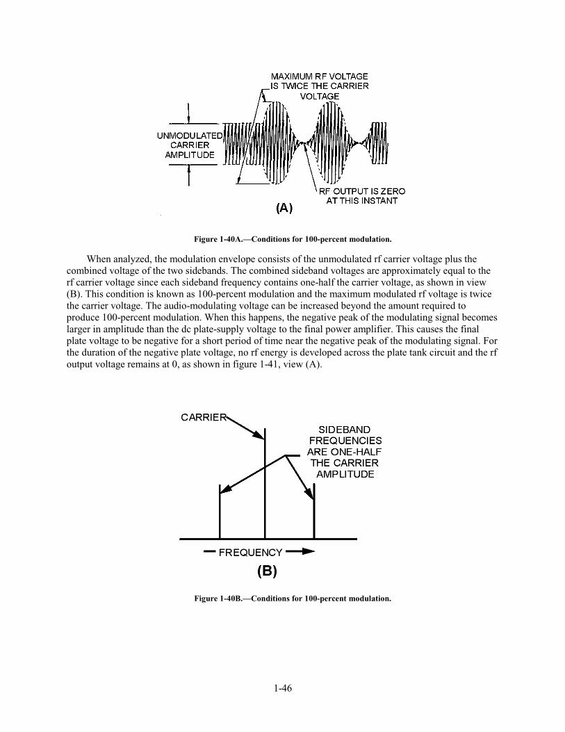
1-46
Figure 1-40A.—Conditions for 100-percent modulation.
When analyzed, the modulation envelope consists of the unmodulated rf carrier voltage plus the combined voltage of the two sidebands. The combined sideband voltages are approximately equal to the rf carrier voltage since each sideband frequency contains one-half the carrier voltage, as shown in view (B). This condition is known as 100-percent modulation and the maximum modulated rf voltage is twice the carrier voltage. The audio-modulating voltage can be increased beyond the amount required to produce 100-percent modulation. When this happens, the negative peak of the modulating signal becomes larger in amplitude than the dc plate-supply voltage to the final power amplifier. This causes the final plate voltage to be negative for a short period of time near the negative peak of the modulating signal. For the duration of the negative plate voltage, no rf energy is developed across the plate tank circuit and the rf output voltage remains at 0, as shown in figure 1-41, view (A).
Figure 1-40B.—Conditions for 100-percent modulation.
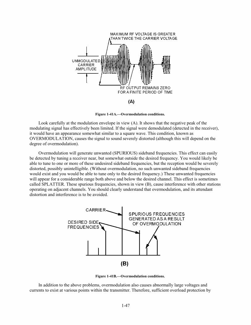
1-47
Figure 1-41A.—Overmodulation conditions.
Look carefully at the modulation envelope in view (A). It shows that the negative peak of the modulating signal has effectively been limited. If the signal were demodulated (detected in the receiver), it would have an appearance somewhat similar to a square wave. This condition, known as OVERMODULATION, causes the signal to sound severely distorted (although this will depend on the degree of overmodulation).
Overmodulation will generate unwanted (SPURIOUS) sideband frequencies. This effect can easily be detected by tuning a receiver near, but somewhat outside the desired frequency. You would likely be able to tune to one or more of these undesired sideband frequencies, but the reception would be severely distorted, possibly unintelligible. (Without overmodulation, no such unwanted sideband frequencies would exist and you would be able to tune only to the desired frequency.) These unwanted frequencies will appear for a considerable range both above and below the desired channel. This effect is sometimes called SPLATTER. These spurious frequencies, shown in view (B), cause interference with other stations operating on adjacent channels. You should clearly understand that overmodulation, and its attendant distortion and interference is to be avoided.
Figure 1-41B.—Overmodulation conditions.
In addition to the above problems, overmodulation also causes abnormally large voltages and currents to exist at various points within the transmitter. Therefore, sufficient overload protection by
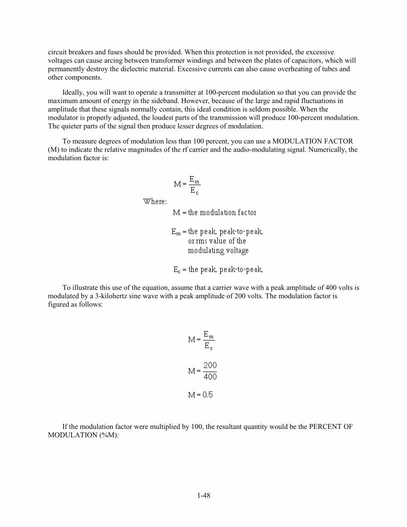
1-48
circuit breakers and fuses should be provided. When this protection is not provided, the excessive voltages can cause arcing between transformer windings and between the plates of capacitors, which will permanently destroy the dielectric material. Excessive currents can also cause overheating of tubes and other components.
Ideally, you will want to operate a transmitter at 100-percent modulation so that you can provide the maximum amount of energy in the sideband. However, because of the large and rapid fluctuations in amplitude that these signals normally contain, this ideal condition is seldom possible. When the modulator is properly adjusted, the loudest parts of the transmission will produce 100-percent modulation. The quieter parts of the signal then produce lesser degrees of modulation.
To measure degrees of modulation less than 100 percent, you can use a MODULATION FACTOR (M) to indicate the relative magnitudes of the rf carrier and the audio-modulating signal. Numerically, the modulation factor is:
To illustrate this use of the equation, assume that a carrier wave with a peak amplitude of 400 volts is modulated by a 3-kilohertz sine wave with a peak amplitude of 200 volts. The modulation factor is figured as follows:
If the modulation factor were multiplied by 100, the resultant quantity would be the PERCENT OF MODULATION (%M):
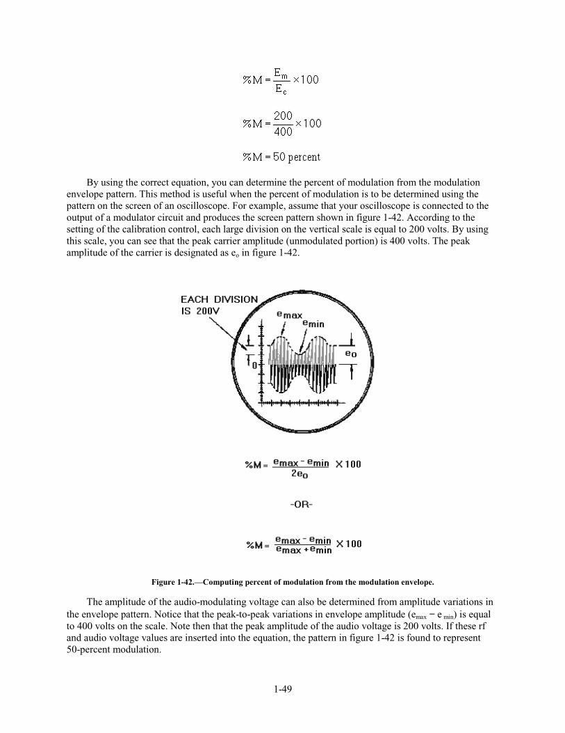
1-49
By using the correct equation, you can determine the percent of modulation from the modulation envelope pattern. This method is useful when the percent of modulation is to be determined using the pattern on the screen of an oscilloscope. For example, assume that your oscilloscope is connected to the output of a modulator circuit and produces the screen pattern shown in figure 1-42. According to the setting of the calibration control, each large division on the vertical scale is equal to 200 volts. By using this scale, you can see that the peak carrier amplitude (unmodulated portion) is 400 volts. The peak amplitude of the carrier is designated as eo in figure 1-42.
Figure 1-42.—Computing percent of modulation from the modulation envelope.
The amplitude of the audio-modulating voltage can also be determined from amplitude variations in the envelope pattern. Notice that the peak-to-peak variations in envelope amplitude (emax − e min) is equal to 400 volts on the scale. Note then that the peak amplitude of the audio voltage is 200 volts. If these rf and audio voltage values are inserted into the equation, the pattern in figure 1-42 is found to represent 50-percent modulation.
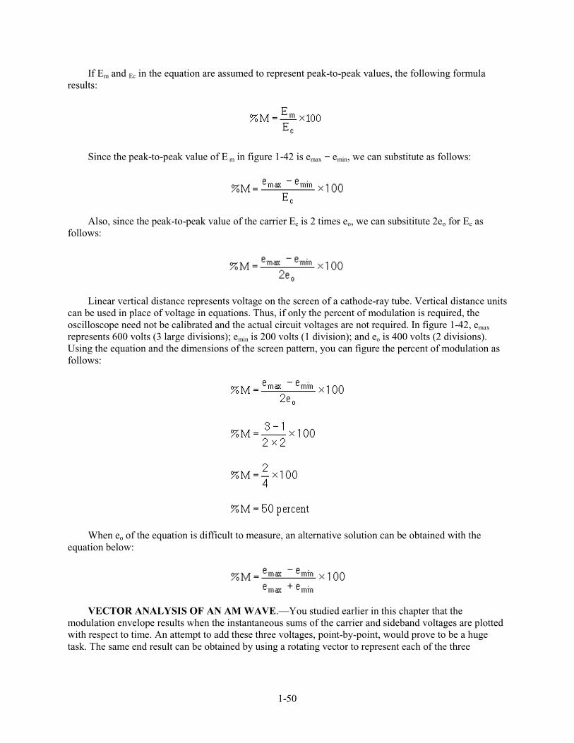
1-50
If Em and Ec in the equation are assumed to represent peak-to-peak values, the following formula results:
Since the peak-to-peak value of E m in figure 1-42 is emax − emin, we can substitute as follows:
Also, since the peak-to-peak value of the carrier Ec is 2 times eo, we can subsititute 2eo for Ec as follows:
Linear vertical distance represents voltage on the screen of a cathode-ray tube. Vertical distance units can be used in place of voltage in equations. Thus, if only the percent of modulation is required, the oscilloscope need not be calibrated and the actual circuit voltages are not required. In figure 1-42, emax represents 600 volts (3 large divisions); emin is 200 volts (1 division); and eo is 400 volts (2 divisions). Using the equation and the dimensions of the screen pattern, you can figure the percent of modulation as follows:
When eo of the equation is difficult to measure, an alternative solution can be obtained with the equation below:
VECTOR ANALYSIS OF AN AM WAVE.—You studied earlier in this chapter that the modulation envelope results when the instantaneous sums of the carrier and sideband voltages are plotted with respect to time. An attempt to add these three voltages, point-by-point, would prove to be a huge task. The same end result can be obtained by using a rotating vector to represent each of the three
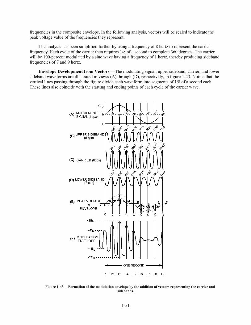
1-51
frequencies in the composite envelope. In the following analysis, vectors will be scaled to indicate the peak voltage value of the frequencies they represent.
The analysis has been simplified further by using a frequency of 8 hertz to represent the carrier frequency. Each cycle of the carrier then requires 1/8 of a second to complete 360 degrees. The carrier will be 100-percent modulated by a sine wave having a frequency of 1 hertz, thereby producing sideband frequencies of 7 and 9 hertz.
Envelope Development from Vectors.—The modulating signal, upper sideband, carrier, and lower sideband waveforms are illustrated in views (A) through (D), respectively, in figure 1-43. Notice that the vertical lines passing through the figure divide each waveform into segments of 1/8 of a second each. These lines also coincide with the starting and ending points of each cycle of the carrier wave.
Figure 1-43.—Formation of the modulation envelope by the addition of vectors representing the carrier and sidebands.
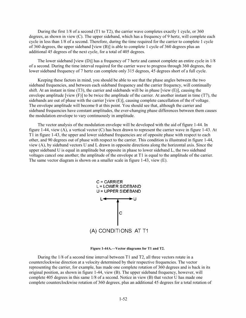
1-52
During the first 1/8 of a second (T1 to T2), the carrier wave completes exactly 1 cycle, or 360 degrees, as shown in view (C). The upper sideband, which has a frequency of 9 hertz, will complete each cycle in less than 1/8 of a second. Therefore, during the time required for the carrier to complete 1 cycle of 360 degrees, the upper sideband [view (B)] is able to complete 1 cycle of 360 degrees plus an additional 45 degrees of the next cycle, for a total of 405 degrees.
The lower sideband [view (D)] has a frequency of 7 hertz and cannot complete an entire cycle in 1/8 of a second. During the time interval required for the carrier wave to progress through 360 degrees, the lower sideband frequency of 7 hertz can complete only 315 degrees, 45 degrees short of a full cycle.
Keeping these factors in mind, you should be able to see that the phase angles between the two sideband frequencies, and between each sideband frequency and the carrier frequency, will continually shift. At an instant in time (T3), the carrier and sidebands will be in phase [view (E)], causing the envelope amplitude [view (F)] to be twice the amplitude of the carrier. At another instant in time (T7), the sidebands are out of phase with the carrier [view (E)], causing complete cancellation of the rf voltage. The envelope amplitude will become 0 at this point. You should see that, although the carrier and sideband frequencies have constant amplitudes, the ever-changing phase differences between them causes the modulation envelope to vary continuously in amplitude.
The vector analysis of the modulation envelope will be developed with the aid of figure 1-44. In figure 1-44, view (A), a vertical vector (C) has been drawn to represent the carrier wave in figure 1-43. At T1 in figure 1-43, the upper and lower sideband frequencies are of opposite phase with respect to each other, and 90 degrees out of phase with respect to the carrier. This condition is illustrated in figure 1-44, view (A), by sideband vectors U and L drawn in opposite directions along the horizontal axis. Since the upper sideband U is equal in amplitude but opposite in phase to lower sideband L, the two sideband voltages cancel one another; the amplitude of the envelope at T1 is equal to the amplitude of the carrier. The same vector diagram is shown on a smaller scale in figure 1-43, view (E).
Figure 1-44A.—Vector diagrams for T1 and T2.
During the 1/8 of a second time interval between T1 and T2, all three vectors rotate in a counterclockwise direction at a velocity determined by their respective frequencies. The vector representing the carrier, for example, has made one complete rotation of 360 degrees and is back in its original position, as shown in figure 1-44, view (B). The upper sideband frequency, however, will complete 405 degrees in this same 1/8 of a second. Notice in view (B) that vector U has made one complete counterclockwise rotation of 360 degrees, plus an additional 45 degrees for a total rotation of
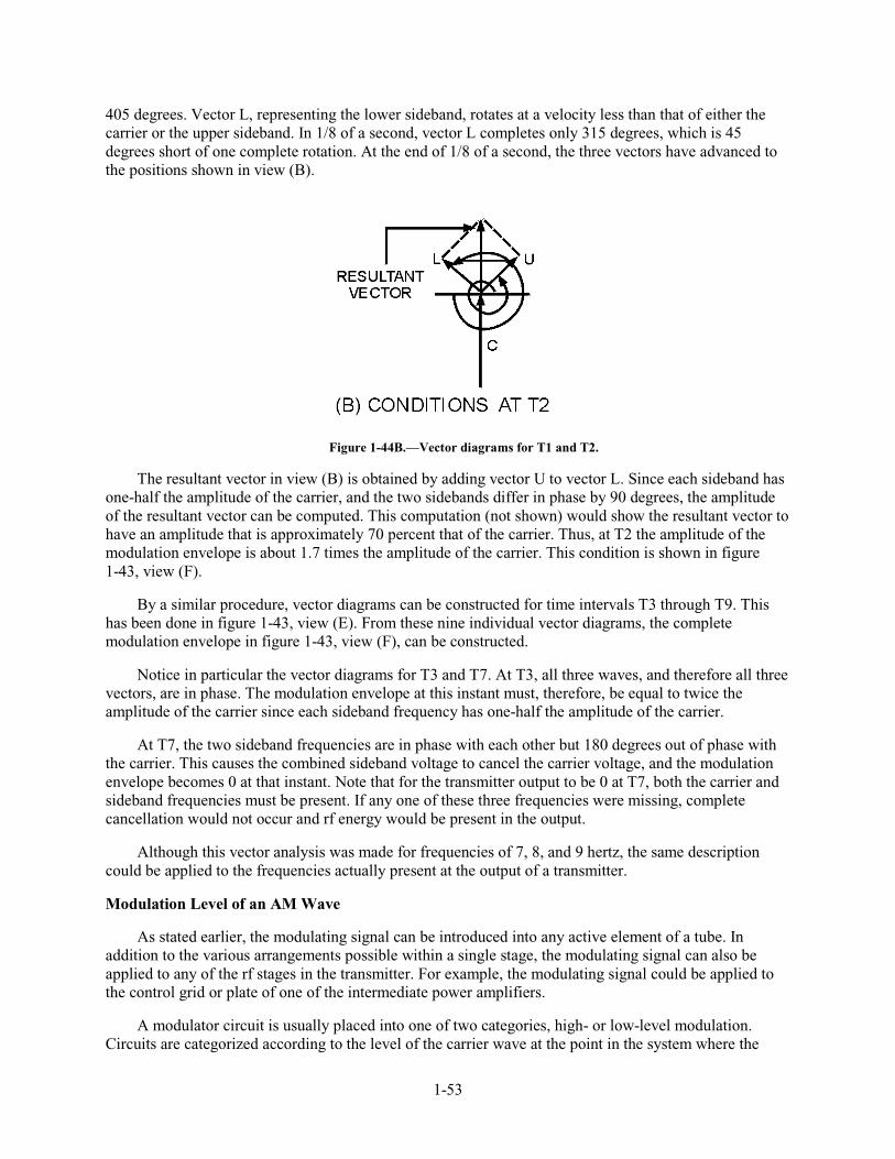
1-53
405 degrees. Vector L, representing the lower sideband, rotates at a velocity less than that of either the carrier or the upper sideband. In 1/8 of a second, vector L completes only 315 degrees, which is 45 degrees short of one complete rotation. At the end of 1/8 of a second, the three vectors have advanced to the positions shown in view (B).
Figure 1-44B.—Vector diagrams for T1 and T2.
The resultant vector in view (B) is obtained by adding vector U to vector L. Since each sideband has one-half the amplitude of the carrier, and the two sidebands differ in phase by 90 degrees, the amplitude of the resultant vector can be computed. This computation (not shown) would show the resultant vector to have an amplitude that is approximately 70 percent that of the carrier. Thus, at T2 the amplitude of the modulation envelope is about 1.7 times the amplitude of the carrier. This condition is shown in figure 1-43, view (F).
By a similar procedure, vector diagrams can be constructed for time intervals T3 through T9. This has been done in figure 1-43, view (E). From these nine individual vector diagrams, the complete modulation envelope in figure 1-43, view (F), can be constructed.
Notice in particular the vector diagrams for T3 and T7. At T3, all three waves, and therefore all three vectors, are in phase. The modulation envelope at this instant must, therefore, be equal to twice the amplitude of the carrier since each sideband frequency has one-half the amplitude of the carrier.
At T7, the two sideband frequencies are in phase with each other but 180 degrees out of phase with the carrier. This causes the combined sideband voltage to cancel the carrier voltage, and the modulation envelope becomes 0 at that instant. Note that for the transmitter output to be 0 at T7, both the carrier and sideband frequencies must be present. If any one of these three frequencies were missing, complete cancellation would not occur and rf energy would be present in the output.
Although this vector analysis was made for frequencies of 7, 8, and 9 hertz, the same description could be applied to the frequencies actually present at the output of a transmitter.
Modulation Level of an AM Wave
As stated earlier, the modulating signal can be introduced into any active element of a tube. In addition to the various arrangements possible within a single stage, the modulating signal can also be applied to any of the rf stages in the transmitter. For example, the modulating signal could be applied to the control grid or plate of one of the intermediate power amplifiers.
A modulator circuit is usually placed into one of two categories, high- or low-level modulation. Circuits are categorized according to the level of the carrier wave at the point in the system where the
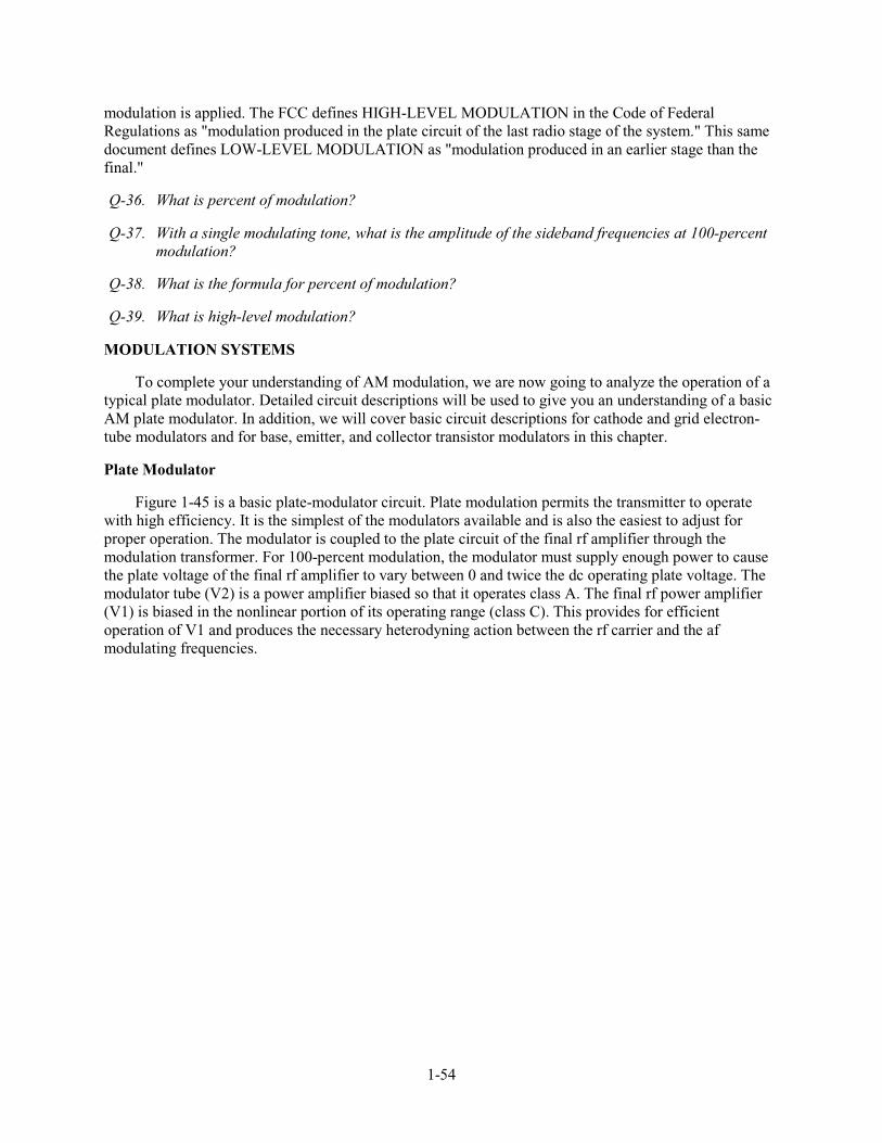
1-54
modulation is applied. The FCC defines HIGH-LEVEL MODULATION in the Code of Federal Regulations as "modulation produced in the plate circuit of the last radio stage of the system." This same document defines LOW-LEVEL MODULATION as "modulation produced in an earlier stage than the final."
Q-36. What is percent of modulation?
Q-37. With a single modulating tone, what is the amplitude of the sideband frequencies at 100-percent modulation?
Q-38. What is the formula for percent of modulation?
Q-39. What is high-level modulation?
MODULATION SYSTEMS
To complete your understanding of AM modulation, we are now going to analyze the operation of a typical plate modulator. Detailed circuit descriptions will be used to give you an understanding of a basic AM plate modulator. In addition, we will cover basic circuit descriptions for cathode and grid electron-tube modulators and for base, emitter, and collector transistor modulators in this chapter.
Plate Modulator
Figure 1-45 is a basic plate-modulator circuit. Plate modulation permits the transmitter to operate with high efficiency. It is the simplest of the modulators available and is also the easiest to adjust for proper operation. The modulator is coupled to the plate circuit of the final rf amplifier through the modulation transformer. For 100-percent modulation, the modulator must supply enough power to cause the plate voltage of the final rf amplifier to vary between 0 and twice the dc operating plate voltage. The modulator tube (V2) is a power amplifier biased so that it operates class A. The final rf power amplifier (V1) is biased in the nonlinear portion of its operating range (class C). This provides for efficient operation of V1 and produces the necessary heterodyning action between the rf carrier and the af modulating frequencies.

1-55
Figure 1-45.—Plate-modulation circuit.
PLATE MODULATOR CIRCUIT OPERATION.—Figure 1-46, views (A) through (E), shows the waveforms associated with the plate-modulator circuit shown in figure 1-45. Refer to these two figures throughout the following discussion.
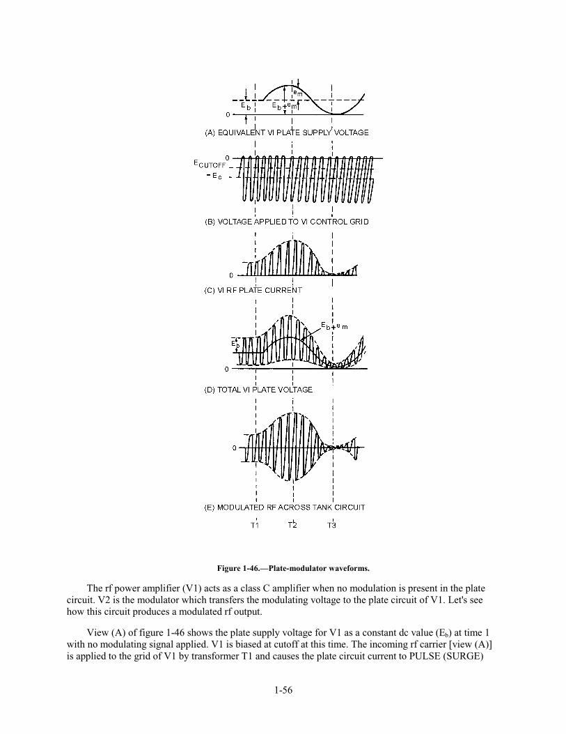
1-56
Figure 1-46.—Plate-modulator waveforms.
The rf power amplifier (V1) acts as a class C amplifier when no modulation is present in the plate circuit. V2 is the modulator which transfers the modulating voltage to the plate circuit of V1. Let's see how this circuit produces a modulated rf output.
View (A) of figure 1-46 shows the plate supply voltage for V1 as a constant dc value (Eb) at time 1 with no modulating signal applied. V1 is biased at cutoff at this time. The incoming rf carrier [view (A)] is applied to the grid of V1 by transformer T1 and causes the plate circuit current to PULSE (SURGE)

1-57
each time the grid is driven positive. These rf pulses are referred to as current pulses and are shown in view (C). The plate tank output circuit (T3) is shocked into oscillation by these current pulses and the rf output waveform shown in view (E) is developed. The rf plate voltage waveform is shown in view (D).
An audio-modulating voltage applied to the grid of V2 is amplified by the modulator and coupled to the plate of V1 by modulation transformer T2. The secondary of T2 is in series with the plate-supply voltage (E) of V1. The modulating voltage will either add to or subtract from the plate voltage of V1. This is shown in view (A) at time 2 and time 3. At time 2 in view (A), the plate supply voltage for V1 increases to twice its normal value and the rf plate current pulses double, as shown in view (C). At time 3 in view (A), the supply voltage is reduced to 0 and the rf plate current decreases to 0, as shown in view (C). These changes in rf plate current cause rf tank T3 voltage to double at time 2 and to decrease to 0 at time 3, as shown in view (E). This action results in the modulation envelope shown in view (E) that represents 100-percent modulation. This is transformer-coupled out of tank circuit T3 to an antenna. Because of the oscillating action of tank circuit T3, V1 has to be rated to handle at least four times its normal plate supply voltage (Eb), as shown by the plate voltage waveform in view (D).
Heterodyning the audio frequency intelligence from the modulator (V2) with the carrier in the plate circuit of the final power amplifier (V1) requires a large amount of audio power. All of the power or voltage that contains the intelligence must come from the modulator stage. This is why plate modulation is called high-level modulation.
The heterodyning action in the plate modulator effectively changes an audio frequency to a different part of the frequency spectrum. This action allows antennas and equipment of practical sizes to be used to transmit the intelligence. Now, let's look at several other typical modulators.
Collector-Injection Modulator
The COLLECTOR-INJECTION MODULATOR is the transistor equivalent of the electron-tube AM plate modulator. This transistor modulator can be used for low-level or relatively high-level modulation. It is referred to as relatively high-level modulation because, at the present time, transistors are limited in their power-handling capability. As illustrated in figure 1-47, the circuit design for a transistor collector-injection modulator is very similar to that of a plate modulator. The collector-injection modulator is capable of 100-percent modulation with medium power-handling capabilities.
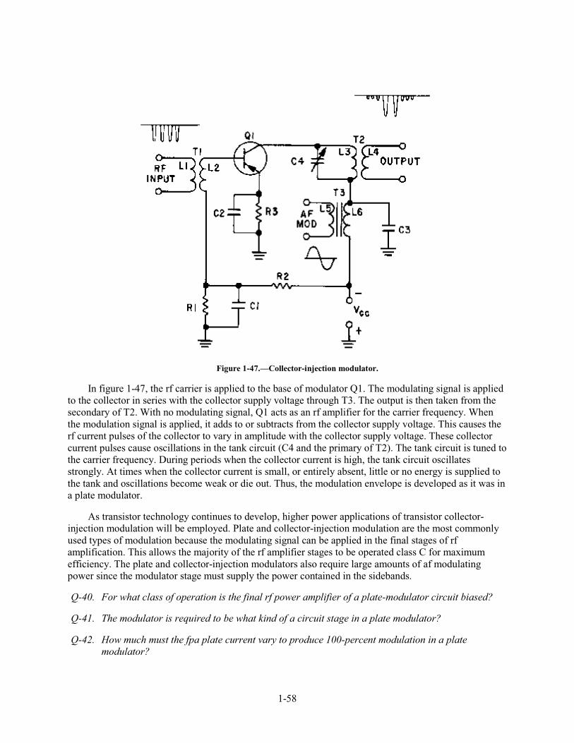
1-58
Figure 1-47.—Collector-injection modulator.
In figure 1-47, the rf carrier is applied to the base of modulator Q1. The modulating signal is applied to the collector in series with the collector supply voltage through T3. The output is then taken from the secondary of T2. With no modulating signal, Q1 acts as an rf amplifier for the carrier frequency. When the modulation signal is applied, it adds to or subtracts from the collector supply voltage. This causes the rf current pulses of the collector to vary in amplitude with the collector supply voltage. These collector current pulses cause oscillations in the tank circuit (C4 and the primary of T2). The tank circuit is tuned to the carrier frequency. During periods when the collector current is high, the tank circuit oscillates strongly. At times when the collector current is small, or entirely absent, little or no energy is supplied to the tank and oscillations become weak or die out. Thus, the modulation envelope is developed as it was in a plate modulator.
As transistor technology continues to develop, higher power applications of transistor collector-injection modulation will be employed. Plate and collector-injection modulation are the most commonly used types of modulation because the modulating signal can be applied in the final stages of rf amplification. This allows the majority of the rf amplifier stages to be operated class C for maximum efficiency. The plate and collector-injection modulators also require large amounts of af modulating power since the modulator stage must supply the power contained in the sidebands.
Q-40. For what class of operation is the final rf power amplifier of a plate-modulator circuit biased?
Q-41. The modulator is required to be what kind of a circuit stage in a plate modulator?
Q-42. How much must the fpa plate current vary to produce 100-percent modulation in a plate modulator?
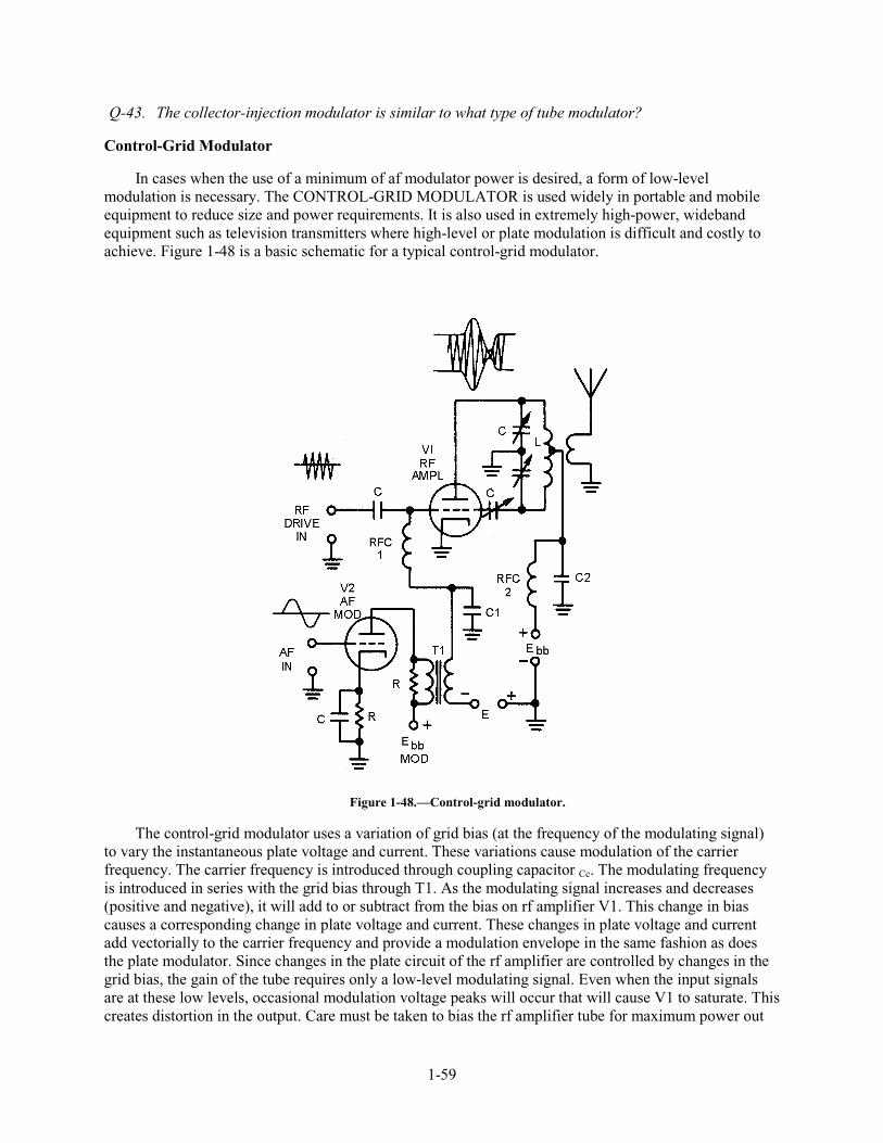
1-59
Q-43. The collector-injection modulator is similar to what type of tube modulator?
Control-Grid Modulator
In cases when the use of a minimum of af modulator power is desired, a form of low-level modulation is necessary. The CONTROL-GRID MODULATOR is used widely in portable and mobile equipment to reduce size and power requirements. It is also used in extremely high-power, wideband equipment such as television transmitters where high-level or plate modulation is difficult and costly to achieve. Figure 1-48 is a basic schematic for a typical control-grid modulator.
Figure 1-48.—Control-grid modulator.
The control-grid modulator uses a variation of grid bias (at the frequency of the modulating signal) to vary the instantaneous plate voltage and current. These variations cause modulation of the carrier frequency. The carrier frequency is introduced through coupling capacitor Cc. The modulating frequency is introduced in series with the grid bias through T1. As the modulating signal increases and decreases (positive and negative), it will add to or subtract from the bias on rf amplifier V1. This change in bias causes a corresponding change in plate voltage and current. These changes in plate voltage and current add vectorially to the carrier frequency and provide a modulation envelope in the same fashion as does the plate modulator. Since changes in the plate circuit of the rf amplifier are controlled by changes in the grid bias, the gain of the tube requires only a low-level modulating signal. Even when the input signals are at these low levels, occasional modulation voltage peaks will occur that will cause V1 to saturate. This creates distortion in the output. Care must be taken to bias the rf amplifier tube for maximum power out
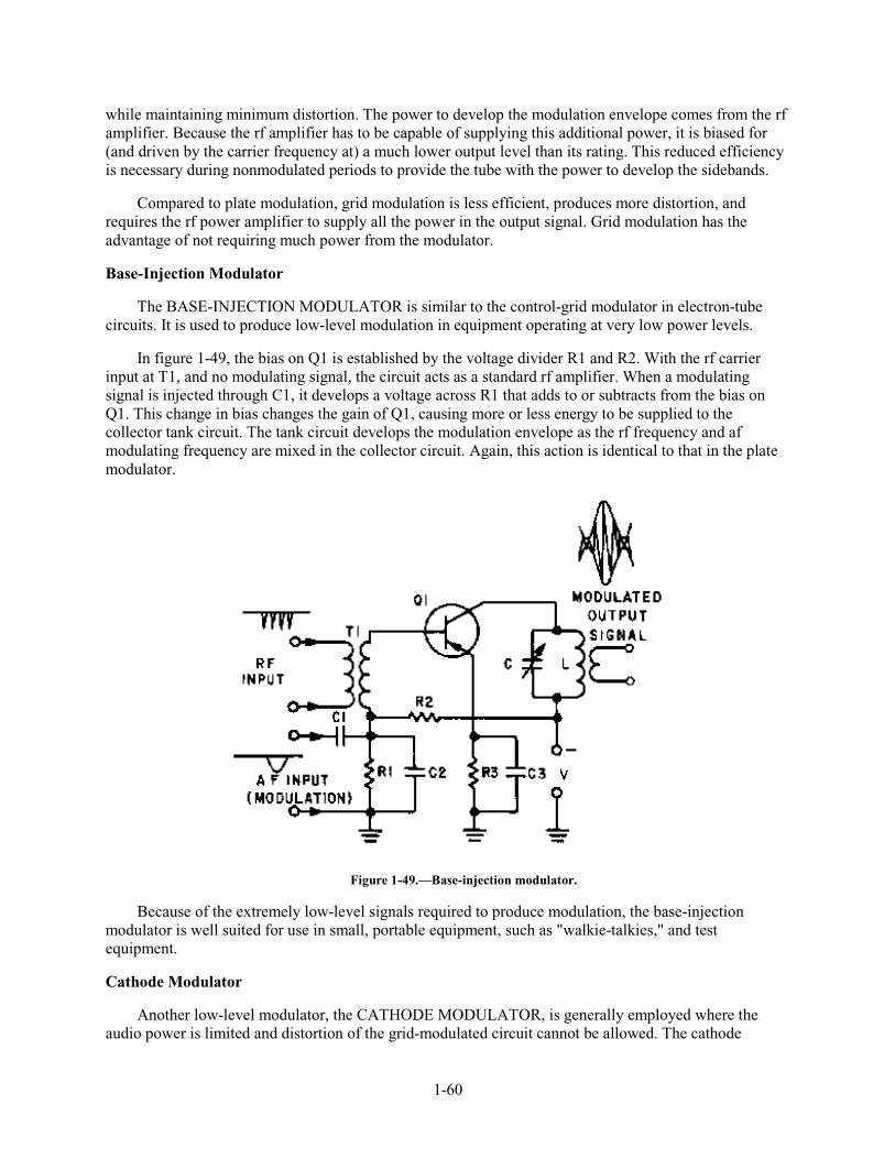
1-60
while maintaining minimum distortion. The power to develop the modulation envelope comes from the rf amplifier. Because the rf amplifier has to be capable of supplying this additional power, it is biased for (and driven by the carrier frequency at) a much lower output level than its rating. This reduced efficiency is necessary during nonmodulated periods to provide the tube with the power to develop the sidebands.
Compared to plate modulation, grid modulation is less efficient, produces more distortion, and requires the rf power amplifier to supply all the power in the output signal. Grid modulation has the advantage of not requiring much power from the modulator.
Base-Injection Modulator
The BASE-INJECTION MODULATOR is similar to the control-grid modulator in electron-tube circuits. It is used to produce low-level modulation in equipment operating at very low power levels.
In figure 1-49, the bias on Q1 is established by the voltage divider R1 and R2. With the rf carrier input at T1, and no modulating signal, the circuit acts as a standard rf amplifier. When a modulating signal is injected through C1, it develops a voltage across R1 that adds to or subtracts from the bias on Q1. This change in bias changes the gain of Q1, causing more or less energy to be supplied to the collector tank circuit. The tank circuit develops the modulation envelope as the rf frequency and af modulating frequency are mixed in the collector circuit. Again, this action is identical to that in the plate modulator.
Figure 1-49.—Base-injection modulator.
Because of the extremely low-level signals required to produce modulation, the base-injection modulator is well suited for use in small, portable equipment, such as "walkie-talkies," and test equipment.
Cathode Modulator
Another low-level modulator, the CATHODE MODULATOR, is generally employed where the audio power is limited and distortion of the grid-modulated circuit cannot be allowed. The cathode

1-61
modulator varies the voltage of the cathode to produce the modulation envelope. Since the cathode is in series with the grid and plate circuits, you should be able see that changing the cathode voltage will effectively change the voltage of the other tube elements. By properly controlling the voltages on the tube, you can cause the cathode modulator to operate in a form of plate modulation with high efficiency. Usually, the cathode modulator is designed to perform about midway between plate and grid modulator levels, using the advantages of each type. When operated between the two levels, the modulator provides a more linear output with moderate efficiency and a modest audio power requirement.
In figure 1-50, the rf carrier is applied to the grid of V1 and the modulating signal is applied in series with the cathode through T1. Since the modulating signal is effectively in series with the grid and plate voltage, the level of modulating voltage required will be determined by the relationships of the three voltages. The modulation takes place in the plate circuit with the plate tank developing the modulation envelope, just as it did in the plate modulator.
Figure 1-50.—Cathode modulator.
Emitter-Injection Modulator
This is the transistor equivalent of the cathode modulator. The EMITTER-INJECTION MODULATOR has the same characteristics as the base-injection modulator discussed earlier. It is an
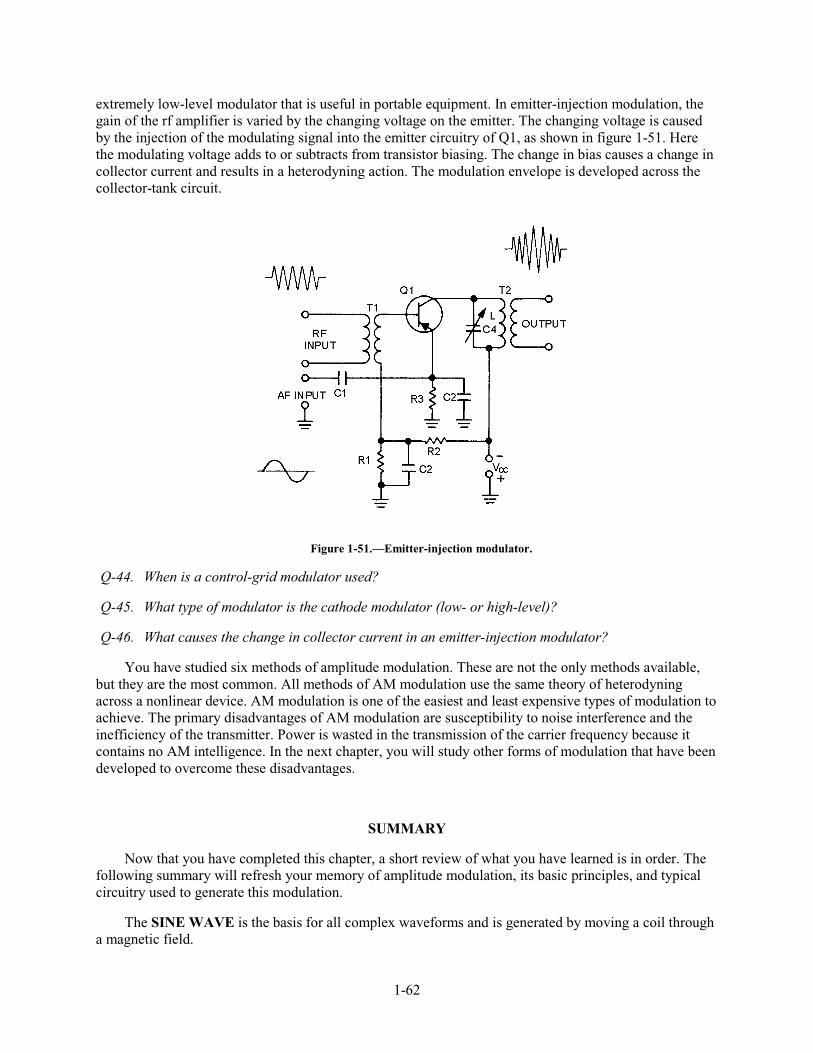
1-62
extremely low-level modulator that is useful in portable equipment. In emitter-injection modulation, the gain of the rf amplifier is varied by the changing voltage on the emitter. The changing voltage is caused by the injection of the modulating signal into the emitter circuitry of Q1, as shown in figure 1-51. Here the modulating voltage adds to or subtracts from transistor biasing. The change in bias causes a change in collector current and results in a heterodyning action. The modulation envelope is developed across the collector-tank circuit.
Figure 1-51.—Emitter-injection modulator.
Q-44. When is a control-grid modulator used?
Q-45. What type of modulator is the cathode modulator (low- or high-level)?
Q-46. What causes the change in collector current in an emitter-injection modulator?
You have studied six methods of amplitude modulation. These are not the only methods available, but they are the most common. All methods of AM modulation use the same theory of heterodyning across a nonlinear device. AM modulation is one of the easiest and least expensive types of modulation to achieve. The primary disadvantages of AM modulation are susceptibility to noise interference and the inefficiency of the transmitter. Power is wasted in the transmission of the carrier frequency because it contains no AM intelligence. In the next chapter, you will study other forms of modulation that have been developed to overcome these disadvantages.
SUMMARY
Now that you have completed this chapter, a short review of what you have learned is in order. The following summary will refresh your memory of amplitude modulation, its basic principles, and typical circuitry used to generate this modulation.
The SINE WAVE is the basis for all complex waveforms and is generated by moving a coil through a magnetic field.
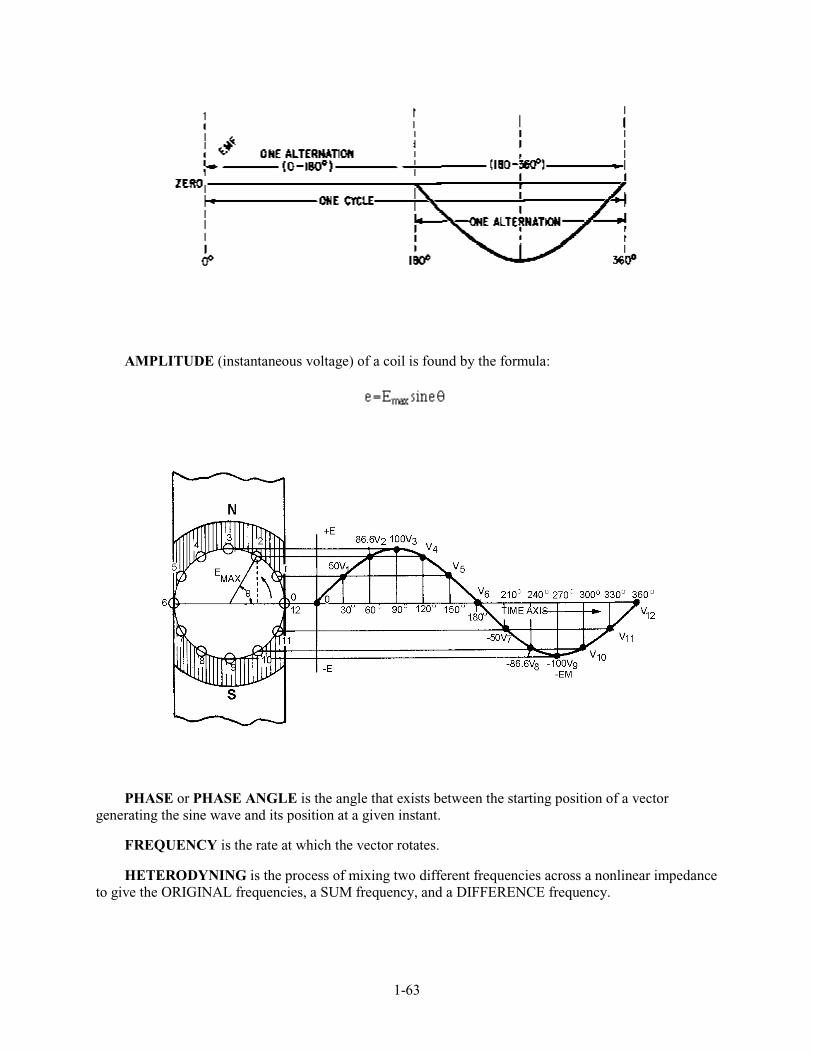
1-63
AMPLITUDE (instantaneous voltage) of a coil is found by the formula:
PHASE or PHASE ANGLE is the angle that exists between the starting position of a vector generating the sine wave and its position at a given instant.
FREQUENCY is the rate at which the vector rotates.
HETERODYNING is the process of mixing two different frequencies across a nonlinear impedance to give the ORIGINAL frequencies, a SUM frequency, and a DIFFERENCE frequency.
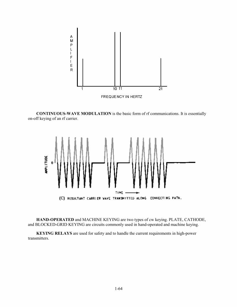
1-64
CONTINUOUS-WAVE MODULATION is the basic form of rf communications. It is essentially on-off keying of an rf carrier.
HAND-OPERATED and MACHINE KEYING are two types of cw keying. PLATE, CATHODE, and BLOCKED-GRID KEYING are circuits commonly used in hand-operated and machine keying.
KEYING RELAYS are used for safety and to handle the current requirements in high-power transmitters.
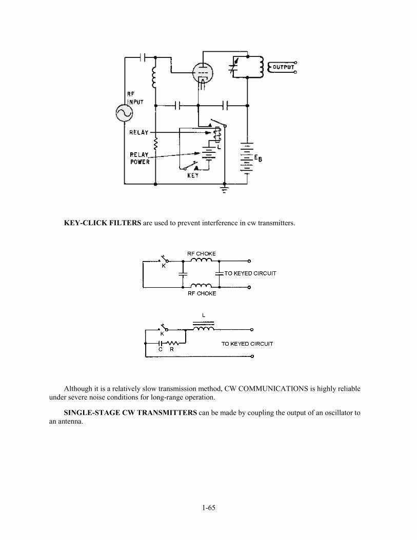
1-65
KEY-CLICK FILTERS are used to prevent interference in cw transmitters.
Although it is a relatively slow transmission method, CW COMMUNICATIONS is highly reliable under severe noise conditions for long-range operation.
SINGLE-STAGE CW TRANSMITTERS can be made by coupling the output of an oscillator to an antenna.
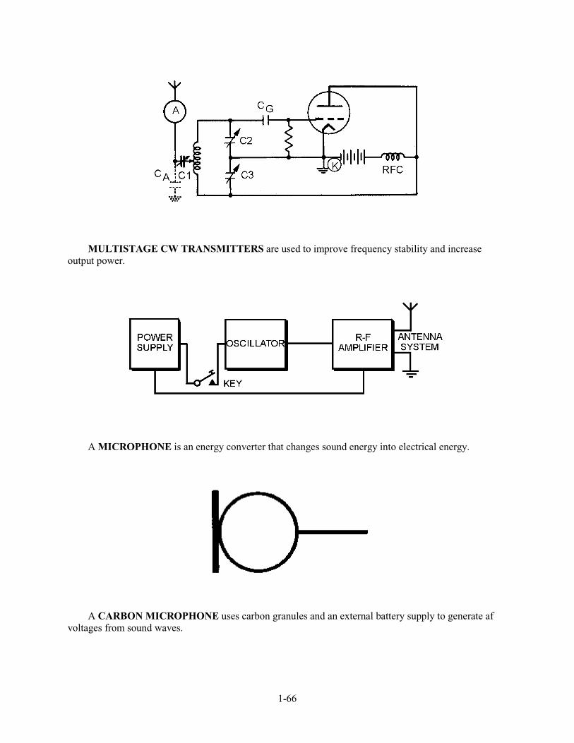
1-66
MULTISTAGE CW TRANSMITTERS are used to improve frequency stability and increase output power.
A MICROPHONE is an energy converter that changes sound energy into electrical energy.
A CARBON MICROPHONE uses carbon granules and an external battery supply to generate af voltages from sound waves.
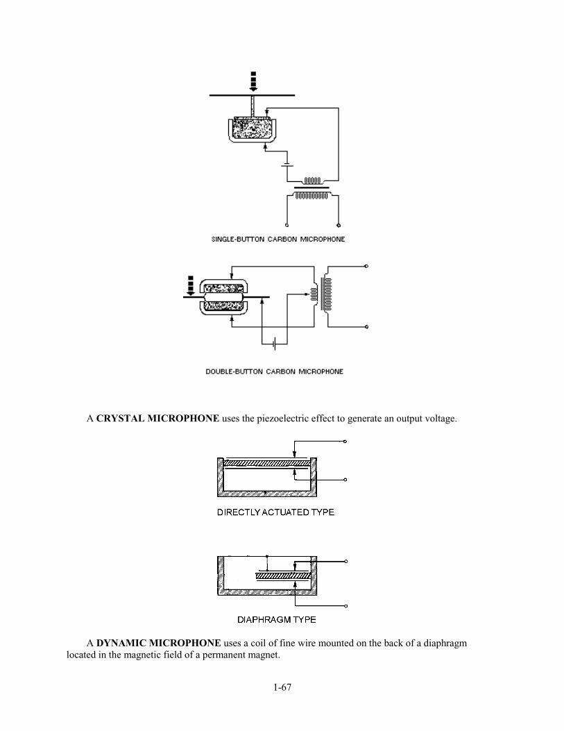
1-67
A CRYSTAL MICROPHONE uses the piezoelectric effect to generate an output voltage.
A DYNAMIC MICROPHONE uses a coil of fine wire mounted on the back of a diaphragm located in the magnetic field of a permanent magnet.

1-68
A MAGNETIC MICROPHONE uses a moving armature in a magnetic field to generate an output.
The FREQUENCY SPECTRUM of a modulated wave can be conveniently illustrated in graph form as frequency versus amplitude.
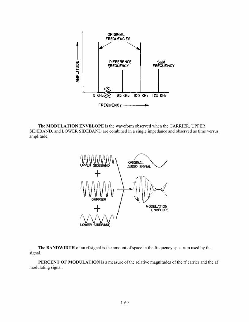
1-69
The MODULATION ENVELOPE is the waveform observed when the CARRIER, UPPER SIDEBAND, and LOWER SIDEBAND are combined in a single impedance and observed as time versus amplitude.
The BANDWIDTH of an rf signal is the amount of space in the frequency spectrum used by the signal.
PERCENT OF MODULATION is a measure of the relative magnitudes of the rf carrier and the af modulating signal.
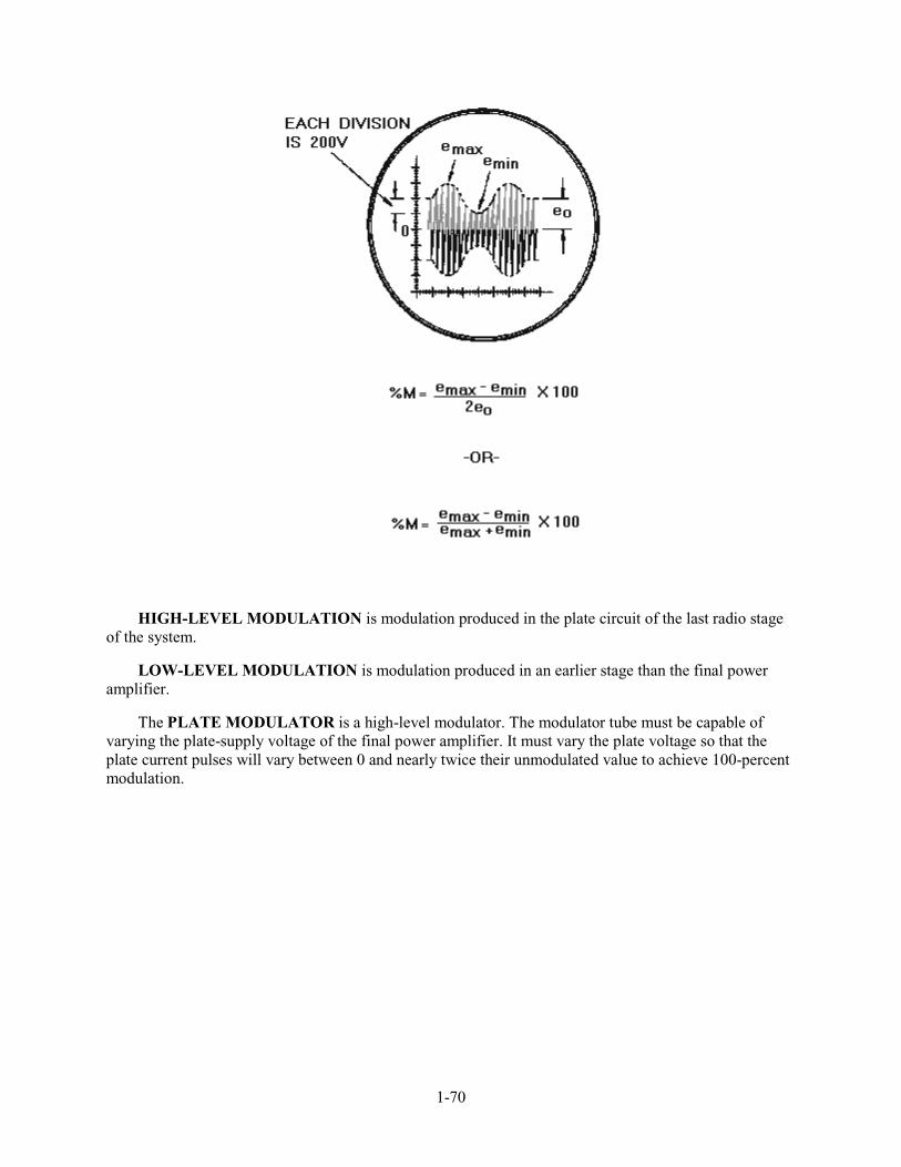
1-70
HIGH-LEVEL MODULATION is modulation produced in the plate circuit of the last radio stage of the system.
LOW-LEVEL MODULATION is modulation produced in an earlier stage than the final power amplifier.
The PLATE MODULATOR is a high-level modulator. The modulator tube must be capable of varying the plate-supply voltage of the final power amplifier. It must vary the plate voltage so that the plate current pulses will vary between 0 and nearly twice their unmodulated value to achieve 100-percent modulation.
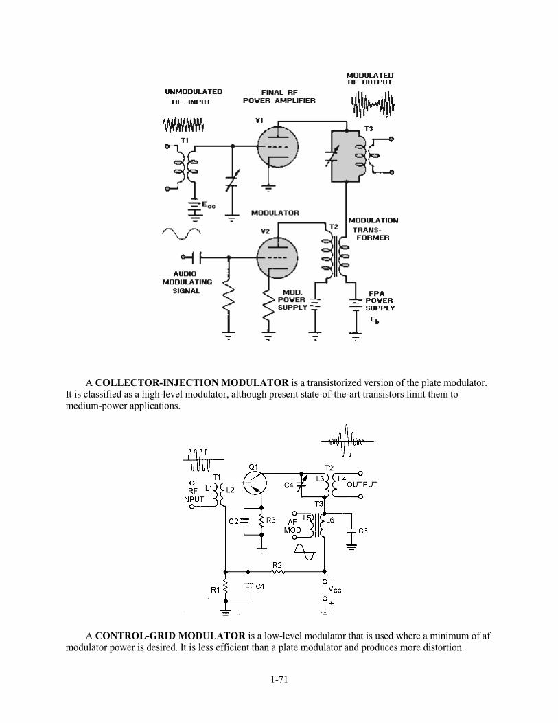
1-71
A COLLECTOR-INJECTION MODULATOR is a transistorized version of the plate modulator. It is classified as a high-level modulator, although present state-of-the-art transistors limit them to medium-power applications.
A CONTROL-GRID MODULATOR is a low-level modulator that is used where a minimum of af modulator power is desired. It is less efficient than a plate modulator and produces more distortion.

1-72
A BASE-INJECTION MODULATOR is used to produce low-level modulation in equipment operating at very low power levels. It is often used in small portable equipment and test equipment.
The CATHODE MODULATOR is a low-level modulator employed where the audio power is limited and the inherent distortion of the grid modulator cannot be tolerated.
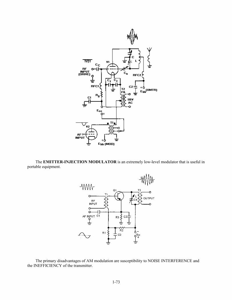
1-73
The EMITTER-INJECTION MODULATOR is an extremely low-level modulator that is useful in portable equipment.
The primary disadvantages of AM modulation are susceptibility to NOISE INTERFERENCE and the INEFFICIENCY of the transmitter.
1-74
ANSWERS TO QUESTIONS Q1. THROUGH Q46.
A-1. Modulation is the impressing of intelligence on a transmission medium.
A-2. May be anything that transmits information, such as light, smoke, sound, wire lines, or radio-frequency waves.
A-3. Mixing two frequencies across a nonlinear impedance.
A-4. The process of recovering intelligence from a modulated carrier.
A-5. The sine wave.
A-6. To represent quantities that have both magnitude and direction.
A-7. Sine ! = opposite side ÷ hypotenuse.
A-8. e = Emax sine !.
A-9. The value at any given point on the sine wave.
A-10. Phase or phase angle.
A-11. The rate at which the vector which is generating the sine wave is rotating.
A-12. The elapsed time from the beginning of cycle to its completion.
A-13. Wavelength = rate of travel × period.
A-14. Process of combining two signal frequencies in a nonlinear device.
A-15. An impedance in which the resulting current is not proportional to the applied voltage.
A-16. The display of electromagnetic energy that is arranged according to wavelength or frequency.
A-17. At least two different frequencies applied to a nonlinear impedance.
A-18. Any method of modulating an electromagnetic carrier frequency by varying its amplitude in accordance with the intelligence.
A-19. A method of generating oscillations, a method of turning the oscillations on and off (keying), and an antenna to radiate the energy.
A-20. Plate keying and cathode keying.
A-21. Machine keying.
A-22. A high degree of clarity even under severe noise conditions, long-range operation, and narrow bandwidth.
A-23. Antenna-to-ground capacitance can cause the oscillator frequency to vary.
A-24. To isolate the oscillator from the antenna and increase the amplitude of the rf oscillations to the required output level.
A-25. To raise the low frequency of a stable oscillator to the vhf range.
1-75
A-26. An energy converter that changes sound energy into electrical energy.
A-27. The changing resistance of carbon granules as pressure is applied to them.
A-28. Background hiss resulting from random changes in the resistance between individual carbon granules.
A-29. The piezoelectric effect.
A-30. A dynamic microphone has a moving coil and the magnetic microphone has a moving armature.
A-31. Rf and af units.
A-32. 100 kilohertz, 5 kilohertz, 95 kilohertz, and 105 kilohertz.
A-33. All of the sum frequencies above the carrier.
A-34. The intelligence is contained in the spacing between the carrier and sideband frequencies.
A-35. The highest modulating frequency.
A-36. The depth or degree of modulation.
A-37. One-half the amplitude of the carrier.
A-38.
A-39. Modulation produced in the plate circuit of the last radio stage of the system.
A-40. Class C.
A-41. Power amplifier.
A-42. Between 0 and nearly two times its unmodulated value.
A-43. Plate modulator.
A-44. In cases when the use of a minimum of af modulator power is desired.
A-45. Low-level.
A-46. Gain is varied by changing the voltage on the emitter.

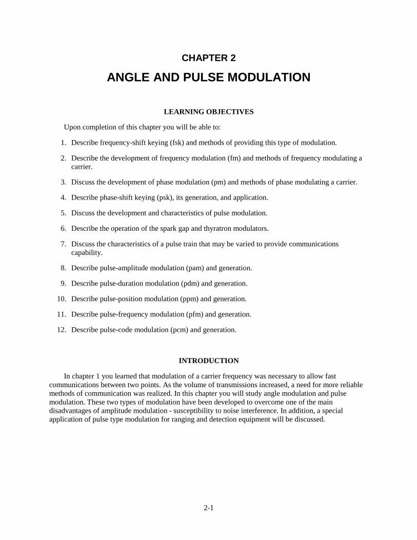
2-1
CHAPTER 2
ANGLE AND PULSE MODULATION
LEARNING OBJECTIVES
Upon completion of this chapter you will be able to:
1. Describe frequency-shift keying (fsk) and methods of providing this type of modulation.
2. Describe the development of frequency modulation (fm) and methods of frequency modulating acarrier.
3. Discuss the development of phase modulation (pm) and methods of phase modulating a carrier.
4. Describe phase-shift keying (psk), its generation, and application.
5. Discuss the development and characteristics of pulse modulation.
6. Describe the operation of the spark gap and thyratron modulators.
7. Discuss the characteristics of a pulse train that may be varied to provide communicationscapability.
8. Describe pulse-amplitude modulation (pam) and generation.
9. Describe pulse-duration modulation (pdm) and generation.
10. Describe pulse-position modulation (ppm) and generation.
11. Describe pulse-frequency modulation (pfm) and generation.
12. Describe pulse-code modulation (pcm) and generation.
INTRODUCTION
In chapter 1 you learned that modulation of a carrier frequency was necessary to allow fastcommunications between two points. As the volume of transmissions increased, a need for more reliablemethods of communication was realized. In this chapter you will study angle modulation and pulsemodulation. These two types of modulation have been developed to overcome one of the maindisadvantages of amplitude modulation - susceptibility to noise interference. In addition, a specialapplication of pulse type modulation for ranging and detection equipment will be discussed.
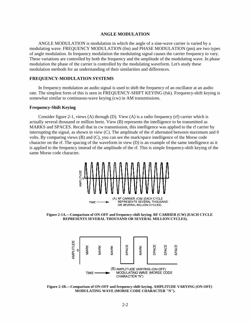
2-2
ANGLE MODULATION
ANGLE MODULATION is modulation in which the angle of a sine-wave carrier is varied by amodulating wave. FREQUENCY MODULATION (fm) and PHASE MODULATION (pm) are two typesof angle modulation. In frequency modulation the modulating signal causes the carrier frequency to vary.These variations are controlled by both the frequency and the amplitude of the modulating wave. In phasemodulation the phase of the carrier is controlled by the modulating waveform. Let’s study thesemodulation methods for an understanding of their similarities and differences.
FREQUENCY-MODULATION SYSTEMS
In frequency modulation an audio signal is used to shift the frequency of an oscillator at an audiorate. The simplest form of this is seen in FREQUENCY-SHIFT KEYING (fsk). Frequency-shift keying issomewhat similar to continuous-wave keying (cw) in AM transmissions.
Frequency-Shift Keying
Consider figure 2-1, views (A) through (D). View (A) is a radio frequency (rf) carrier which isactually several thousand or million hertz. View (B) represents the intelligence to be transmitted asMARKS and SPACES. Recall that in cw transmission, this intelligence was applied to the rf carrier byinterrupting the signal, as shown in view (C). The amplitude of the rf alternated between maximum and 0volts. By comparing views (B) and (C), you can see the mark/space intelligence of the Morse codecharacter on the rf. The spacing of the waveform in view (D) is an example of the same intelligence as itis applied to the frequency instead of the amplitude of the rf. This is simple frequency-shift keying of thesame Morse code character.
Figure 2-1A.—Comparison of ON-OFF and frequency-shift keying. RF CARRIER (CW) (EACH CYCLEREPRESENTS SEVERAL THOUSAND OR SEVERAL MILLION CYCLES).
Figure 2-1B.—Comparison of ON-OFF and frequency-shift keying. AMPLITUDE VARYING (ON-OFF)MODULATING WAVE (MORSE CODE CHARACTER "N").
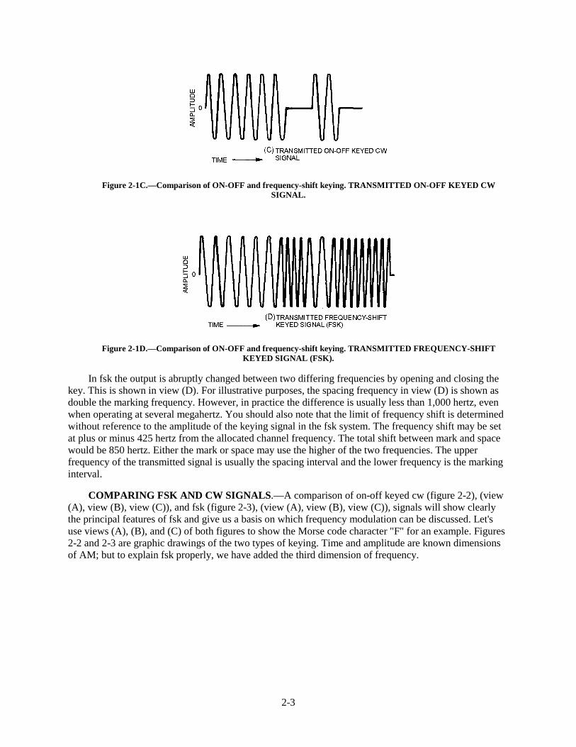
2-3
Figure 2-1C.—Comparison of ON-OFF and frequency-shift keying. TRANSMITTED ON-OFF KEYED CWSIGNAL.
Figure 2-1D.—Comparison of ON-OFF and frequency-shift keying. TRANSMITTED FREQUENCY-SHIFTKEYED SIGNAL (FSK).
In fsk the output is abruptly changed between two differing frequencies by opening and closing thekey. This is shown in view (D). For illustrative purposes, the spacing frequency in view (D) is shown asdouble the marking frequency. However, in practice the difference is usually less than 1,000 hertz, evenwhen operating at several megahertz. You should also note that the limit of frequency shift is determinedwithout reference to the amplitude of the keying signal in the fsk system. The frequency shift may be setat plus or minus 425 hertz from the allocated channel frequency. The total shift between mark and spacewould be 850 hertz. Either the mark or space may use the higher of the two frequencies. The upperfrequency of the transmitted signal is usually the spacing interval and the lower frequency is the markinginterval.
COMPARING FSK AND CW SIGNALS.—A comparison of on-off keyed cw (figure 2-2), (view(A), view (B), view (C)), and fsk (figure 2-3), (view (A), view (B), view (C)), signals will show clearlythe principal features of fsk and give us a basis on which frequency modulation can be discussed. Let'suse views (A), (B), and (C) of both figures to show the Morse code character "F" for an example. Figures2-2 and 2-3 are graphic drawings of the two types of keying. Time and amplitude are known dimensionsof AM; but to explain fsk properly, we have added the third dimension of frequency.
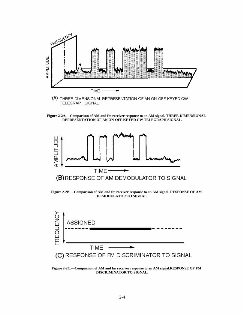
2-4
Figure 2-2A.—Comparison of AM and fm receiver response to an AM signal. THREE-DIMENSIONALREPRESENTATION OF AN ON-OFF KEYED CW TELEGRAPH SIGNAL.
Figure 2-2B.—Comparison of AM and fm receiver response to an AM signal. RESPONSE OF AMDEMODULATOR TO SIGNAL.
Figure 2-2C.—Comparison of AM and fm receiver response to an AM signal.RESPONSE OF FMDISCRIMINATOR TO SIGNAL.
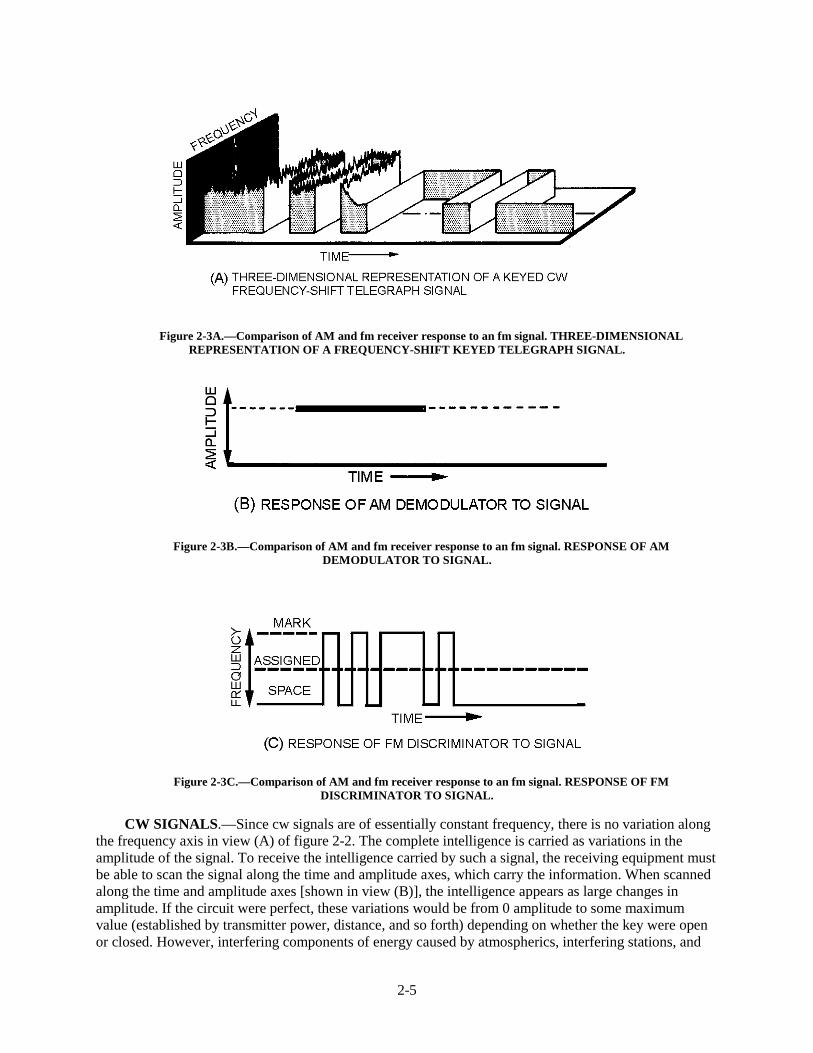
2-5
Figure 2-3A.—Comparison of AM and fm receiver response to an fm signal. THREE-DIMENSIONALREPRESENTATION OF A FREQUENCY-SHIFT KEYED TELEGRAPH SIGNAL.
Figure 2-3B.—Comparison of AM and fm receiver response to an fm signal. RESPONSE OF AMDEMODULATOR TO SIGNAL.
Figure 2-3C.—Comparison of AM and fm receiver response to an fm signal. RESPONSE OF FMDISCRIMINATOR TO SIGNAL.
CW SIGNALS.—Since cw signals are of essentially constant frequency, there is no variation alongthe frequency axis in view (A) of figure 2-2. The complete intelligence is carried as variations in theamplitude of the signal. To receive the intelligence carried by such a signal, the receiving equipment mustbe able to scan the signal along the time and amplitude axes, which carry the information. When scannedalong the time and amplitude axes [shown in view (B)], the intelligence appears as large changes inamplitude. If the circuit were perfect, these variations would be from 0 amplitude to some maximumvalue (established by transmitter power, distance, and so forth) depending on whether the key were openor closed. However, interfering components of energy caused by atmospherics, interfering stations, and
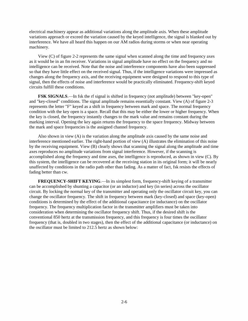
2-6
electrical machinery appear as additional variations along the amplitude axis. When these amplitudevariations approach or exceed the variation caused by the keyed intelligence, the signal is blanked out byinterference. We have all heard this happen on our AM radios during storms or when near operatingmachinery.
View (C) of figure 2-2 represents the same signal when scanned along the time and frequency axesas it would be in an fm receiver. Variations in signal amplitude have no effect on the frequency and nointelligence can be received. Note that the noise and interference components have also been suppressedso that they have little effect on the received signal. Thus, if the intelligence variations were impressed aschanges along the frequency axis, and the receiving equipment were designed to respond to this type ofsignal, then the effects of noise and interference would be practically eliminated. Frequency-shift keyedcircuits fulfill these conditions.
FSK SIGNALS.—In fsk the rf signal is shifted in frequency (not amplitude) between "key-open"and "key-closed" conditions. The signal amplitude remains essentially constant. View (A) of figure 2-3represents the letter "F" keyed as a shift in frequency between mark and space. The normal frequencycondition with the key open is a space. Recall that this may be either the lower or higher frequency. Whenthe key is closed, the frequency instantly changes to the mark value and remains constant during themarking interval. Opening the key again returns the frequency to the space frequency. Midway betweenthe mark and space frequencies is the assigned channel frequency.
Also shown in view (A) is the variation along the amplitude axis caused by the same noise andinterference mentioned earlier. The right-hand portion of view (A) illustrates the elimination of this noiseby the receiving equipment. View (B) clearly shows that scanning the signal along the amplitude and timeaxes reproduces no amplitude variations from signal interference. However, if the scanning isaccomplished along the frequency and time axes, the intelligence is reproduced, as shown in view (C). Bythis system, the intelligence can be recovered at the receiving station in its original form; it will be nearlyunaffected by conditions in the radio path other than fading. As a matter of fact, fsk resists the effects offading better than cw.
FREQUENCY-SHIFT KEYING.—In its simplest form, frequency-shift keying of a transmittercan be accomplished by shunting a capacitor (or an inductor) and key (in series) across the oscillatorcircuit. By locking the normal key of the transmitter and operating only the oscillator circuit key, you canchange the oscillator frequency. The shift in frequency between mark (key-closed) and space (key-open)conditions is determined by the effect of the additional capacitance (or inductance) on the oscillatorfrequency. The frequency multiplication factor in the transmitter amplifiers must be taken intoconsideration when determining the oscillator frequency shift. Thus, if the desired shift is theconventional 850 hertz at the transmission frequency, and this frequency is four times the oscillatorfrequency (that is, doubled in two stages), then the effect of the additional capacitance (or inductance) onthe oscillator must be limited to 212.5 hertz as shown below:
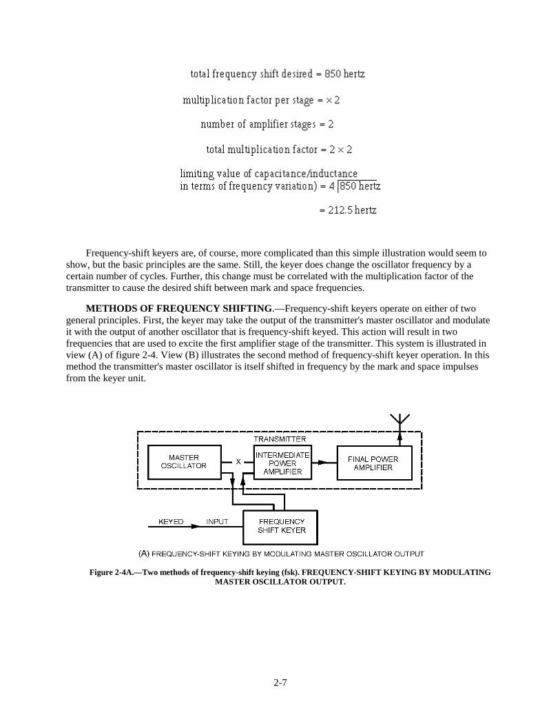
2-7
Frequency-shift keyers are, of course, more complicated than this simple illustration would seem toshow, but the basic principles are the same. Still, the keyer does change the oscillator frequency by acertain number of cycles. Further, this change must be correlated with the multiplication factor of thetransmitter to cause the desired shift between mark and space frequencies.
METHODS OF FREQUENCY SHIFTING.—Frequency-shift keyers operate on either of twogeneral principles. First, the keyer may take the output of the transmitter's master oscillator and modulateit with the output of another oscillator that is frequency-shift keyed. This action will result in twofrequencies that are used to excite the first amplifier stage of the transmitter. This system is illustrated inview (A) of figure 2-4. View (B) illustrates the second method of frequency-shift keyer operation. In thismethod the transmitter's master oscillator is itself shifted in frequency by the mark and space impulsesfrom the keyer unit.
Figure 2-4A.—Two methods of frequency-shift keying (fsk). FREQUENCY-SHIFT KEYING BY MODULATINGMASTER OSCILLATOR OUTPUT.
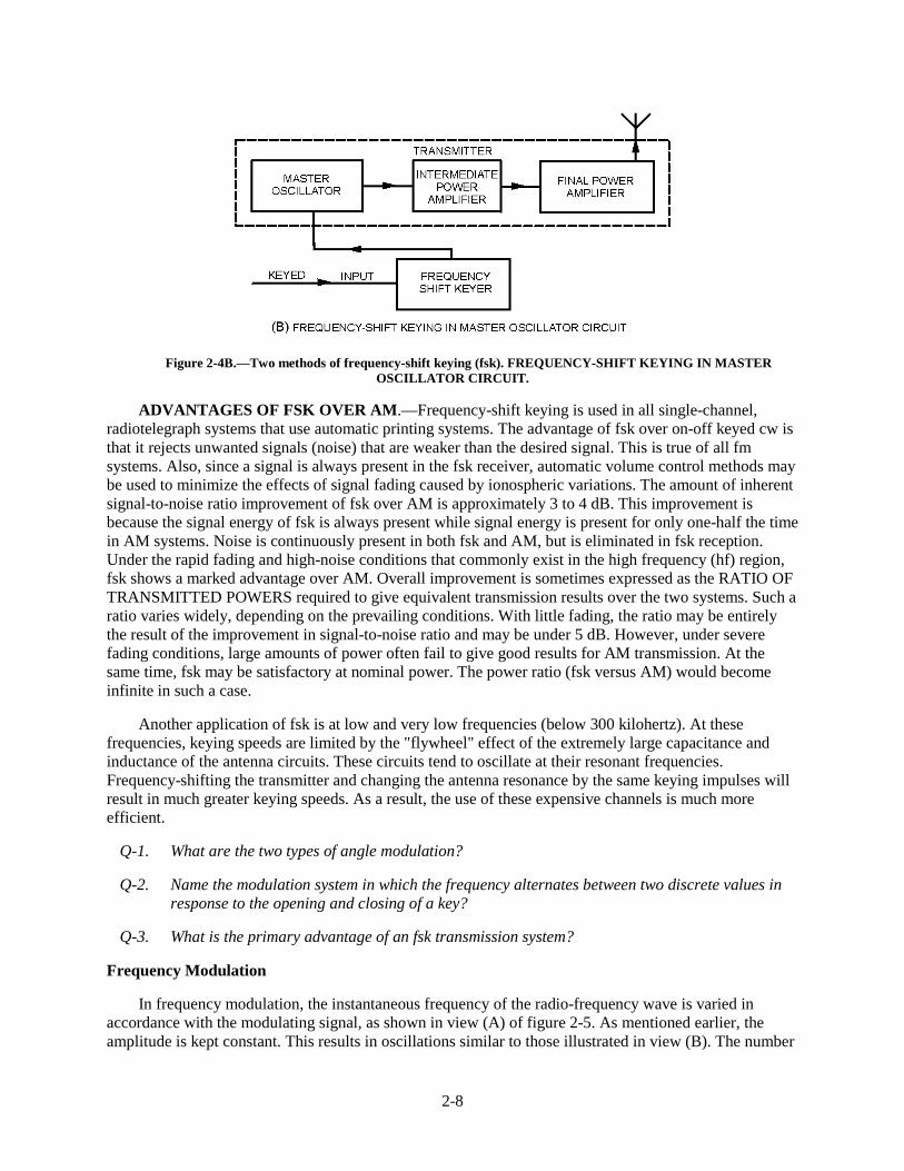
2-8
Figure 2-4B.—Two methods of frequency-shift keying (fsk). FREQUENCY-SHIFT KEYING IN MASTEROSCILLATOR CIRCUIT.
ADVANTAGES OF FSK OVER AM.—Frequency-shift keying is used in all single-channel,radiotelegraph systems that use automatic printing systems. The advantage of fsk over on-off keyed cw isthat it rejects unwanted signals (noise) that are weaker than the desired signal. This is true of all fmsystems. Also, since a signal is always present in the fsk receiver, automatic volume control methods maybe used to minimize the effects of signal fading caused by ionospheric variations. The amount of inherentsignal-to-noise ratio improvement of fsk over AM is approximately 3 to 4 dB. This improvement isbecause the signal energy of fsk is always present while signal energy is present for only one-half the timein AM systems. Noise is continuously present in both fsk and AM, but is eliminated in fsk reception.Under the rapid fading and high-noise conditions that commonly exist in the high frequency (hf) region,fsk shows a marked advantage over AM. Overall improvement is sometimes expressed as the RATIO OFTRANSMITTED POWERS required to give equivalent transmission results over the two systems. Such aratio varies widely, depending on the prevailing conditions. With little fading, the ratio may be entirelythe result of the improvement in signal-to-noise ratio and may be under 5 dB. However, under severefading conditions, large amounts of power often fail to give good results for AM transmission. At thesame time, fsk may be satisfactory at nominal power. The power ratio (fsk versus AM) would becomeinfinite in such a case.
Another application of fsk is at low and very low frequencies (below 300 kilohertz). At thesefrequencies, keying speeds are limited by the "flywheel" effect of the extremely large capacitance andinductance of the antenna circuits. These circuits tend to oscillate at their resonant frequencies.Frequency-shifting the transmitter and changing the antenna resonance by the same keying impulses willresult in much greater keying speeds. As a result, the use of these expensive channels is much moreefficient.
Q-1. What are the two types of angle modulation?
Q-2. Name the modulation system in which the frequency alternates between two discrete values inresponse to the opening and closing of a key?
Q-3. What is the primary advantage of an fsk transmission system?
Frequency Modulation
In frequency modulation, the instantaneous frequency of the radio-frequency wave is varied inaccordance with the modulating signal, as shown in view (A) of figure 2-5. As mentioned earlier, theamplitude is kept constant. This results in oscillations similar to those illustrated in view (B). The number
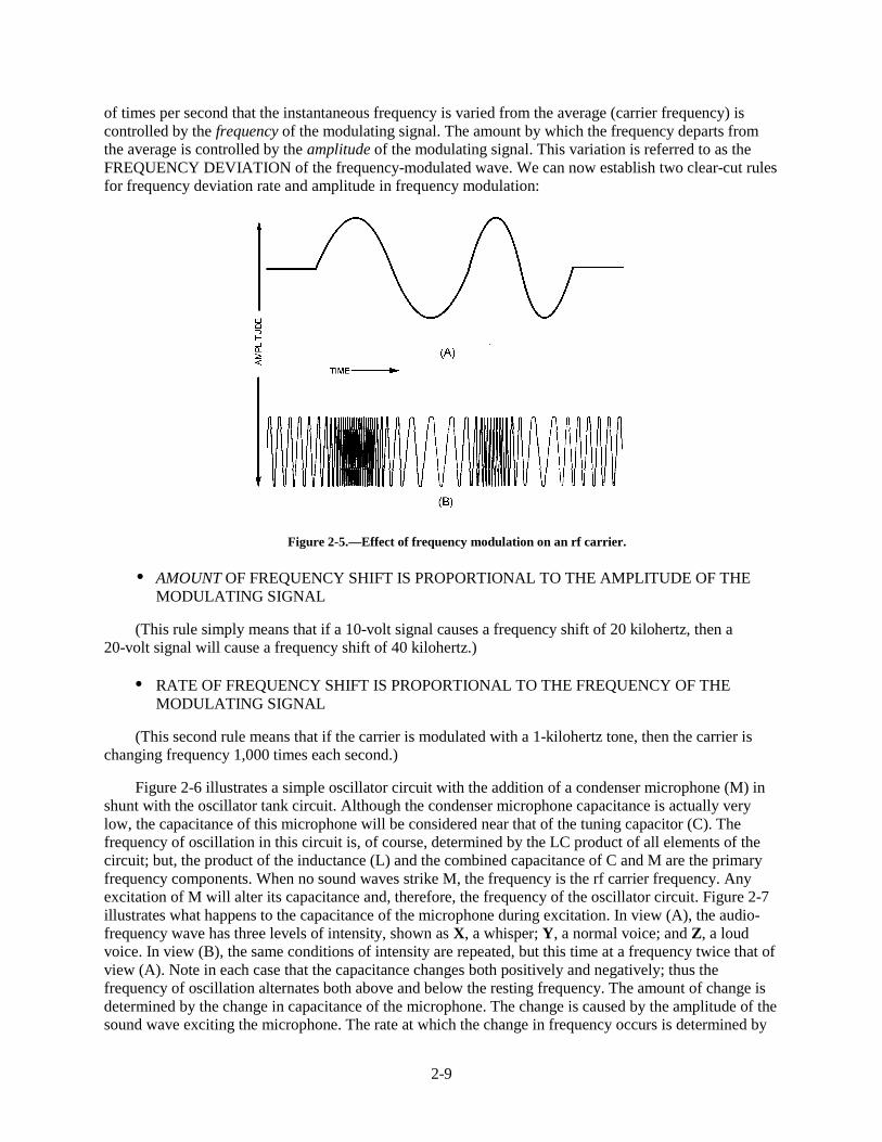
2-9
of times per second that the instantaneous frequency is varied from the average (carrier frequency) iscontrolled by the frequency of the modulating signal. The amount by which the frequency departs fromthe average is controlled by the amplitude of the modulating signal. This variation is referred to as theFREQUENCY DEVIATION of the frequency-modulated wave. We can now establish two clear-cut rulesfor frequency deviation rate and amplitude in frequency modulation:
Figure 2-5.—Effect of frequency modulation on an rf carrier.
• AMOUNT OF FREQUENCY SHIFT IS PROPORTIONAL TO THE AMPLITUDE OF THEMODULATING SIGNAL
(This rule simply means that if a 10-volt signal causes a frequency shift of 20 kilohertz, then a20-volt signal will cause a frequency shift of 40 kilohertz.)
• RATE OF FREQUENCY SHIFT IS PROPORTIONAL TO THE FREQUENCY OF THEMODULATING SIGNAL
(This second rule means that if the carrier is modulated with a 1-kilohertz tone, then the carrier ischanging frequency 1,000 times each second.)
Figure 2-6 illustrates a simple oscillator circuit with the addition of a condenser microphone (M) inshunt with the oscillator tank circuit. Although the condenser microphone capacitance is actually verylow, the capacitance of this microphone will be considered near that of the tuning capacitor (C). Thefrequency of oscillation in this circuit is, of course, determined by the LC product of all elements of thecircuit; but, the product of the inductance (L) and the combined capacitance of C and M are the primaryfrequency components. When no sound waves strike M, the frequency is the rf carrier frequency. Anyexcitation of M will alter its capacitance and, therefore, the frequency of the oscillator circuit. Figure 2-7illustrates what happens to the capacitance of the microphone during excitation. In view (A), the audio-frequency wave has three levels of intensity, shown as X, a whisper; Y, a normal voice; and Z, a loudvoice. In view (B), the same conditions of intensity are repeated, but this time at a frequency twice that ofview (A). Note in each case that the capacitance changes both positively and negatively; thus thefrequency of oscillation alternates both above and below the resting frequency. The amount of change isdetermined by the change in capacitance of the microphone. The change is caused by the amplitude of thesound wave exciting the microphone. The rate at which the change in frequency occurs is determined by
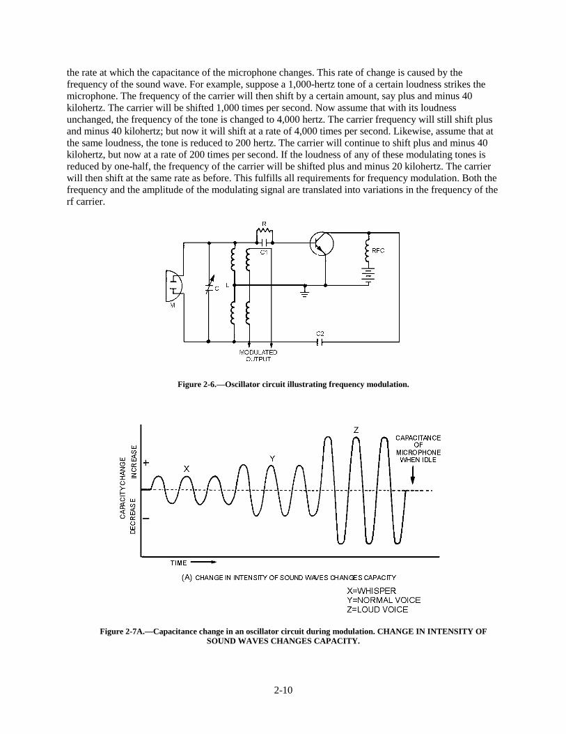
2-10
the rate at which the capacitance of the microphone changes. This rate of change is caused by thefrequency of the sound wave. For example, suppose a 1,000-hertz tone of a certain loudness strikes themicrophone. The frequency of the carrier will then shift by a certain amount, say plus and minus 40kilohertz. The carrier will be shifted 1,000 times per second. Now assume that with its loudnessunchanged, the frequency of the tone is changed to 4,000 hertz. The carrier frequency will still shift plusand minus 40 kilohertz; but now it will shift at a rate of 4,000 times per second. Likewise, assume that atthe same loudness, the tone is reduced to 200 hertz. The carrier will continue to shift plus and minus 40kilohertz, but now at a rate of 200 times per second. If the loudness of any of these modulating tones isreduced by one-half, the frequency of the carrier will be shifted plus and minus 20 kilohertz. The carrierwill then shift at the same rate as before. This fulfills all requirements for frequency modulation. Both thefrequency and the amplitude of the modulating signal are translated into variations in the frequency of therf carrier.
Figure 2-6.—Oscillator circuit illustrating frequency modulation.
Figure 2-7A.—Capacitance change in an oscillator circuit during modulation. CHANGE IN INTENSITY OFSOUND WAVES CHANGES CAPACITY.
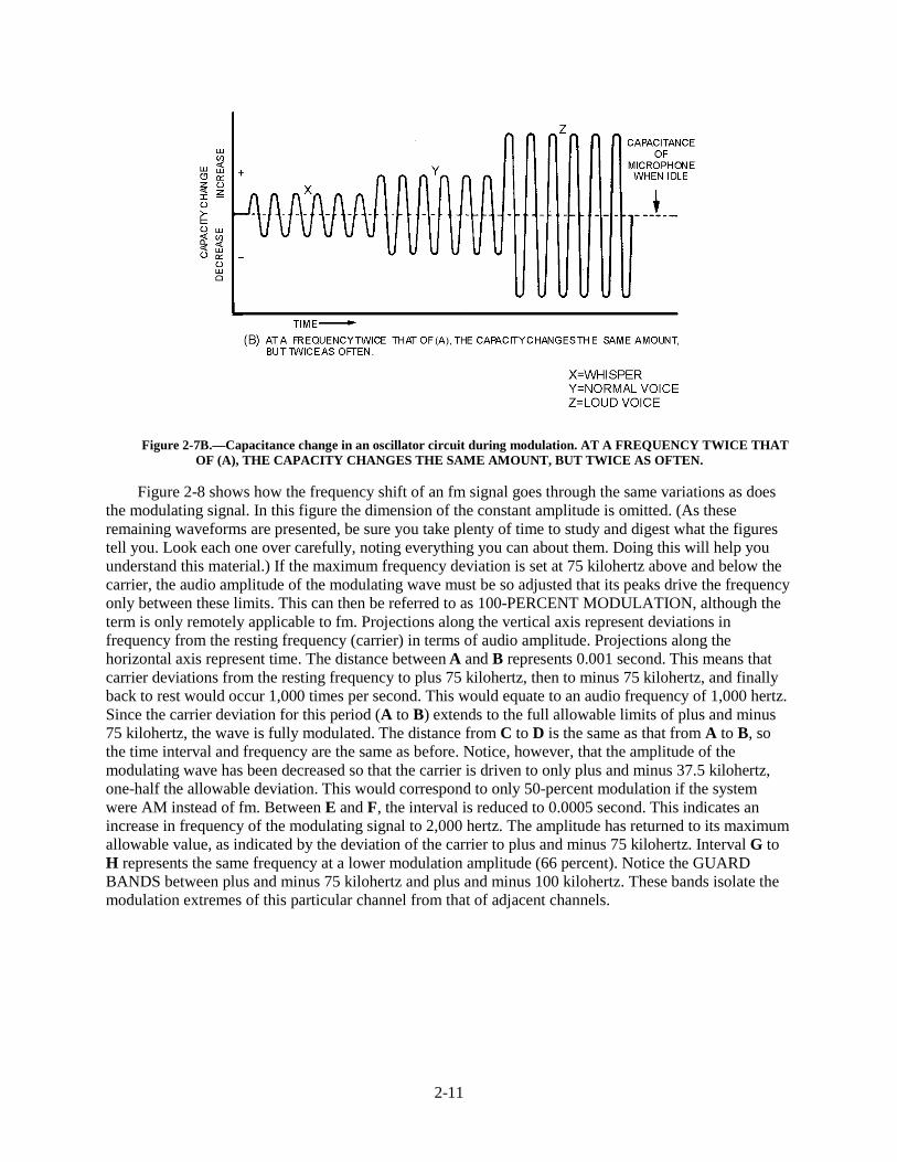
2-11
Figure 2-7B.—Capacitance change in an oscillator circuit during modulation. AT A FREQUENCY TWICE THATOF (A), THE CAPACITY CHANGES THE SAME AMOUNT, BUT TWICE AS OFTEN.
Figure 2-8 shows how the frequency shift of an fm signal goes through the same variations as doesthe modulating signal. In this figure the dimension of the constant amplitude is omitted. (As theseremaining waveforms are presented, be sure you take plenty of time to study and digest what the figurestell you. Look each one over carefully, noting everything you can about them. Doing this will help youunderstand this material.) If the maximum frequency deviation is set at 75 kilohertz above and below thecarrier, the audio amplitude of the modulating wave must be so adjusted that its peaks drive the frequencyonly between these limits. This can then be referred to as 100-PERCENT MODULATION, although theterm is only remotely applicable to fm. Projections along the vertical axis represent deviations infrequency from the resting frequency (carrier) in terms of audio amplitude. Projections along thehorizontal axis represent time. The distance between A and B represents 0.001 second. This means thatcarrier deviations from the resting frequency to plus 75 kilohertz, then to minus 75 kilohertz, and finallyback to rest would occur 1,000 times per second. This would equate to an audio frequency of 1,000 hertz.Since the carrier deviation for this period (A to B) extends to the full allowable limits of plus and minus75 kilohertz, the wave is fully modulated. The distance from C to D is the same as that from A to B, sothe time interval and frequency are the same as before. Notice, however, that the amplitude of themodulating wave has been decreased so that the carrier is driven to only plus and minus 37.5 kilohertz,one-half the allowable deviation. This would correspond to only 50-percent modulation if the systemwere AM instead of fm. Between E and F, the interval is reduced to 0.0005 second. This indicates anincrease in frequency of the modulating signal to 2,000 hertz. The amplitude has returned to its maximumallowable value, as indicated by the deviation of the carrier to plus and minus 75 kilohertz. Interval G toH represents the same frequency at a lower modulation amplitude (66 percent). Notice the GUARDBANDS between plus and minus 75 kilohertz and plus and minus 100 kilohertz. These bands isolate themodulation extremes of this particular channel from that of adjacent channels.
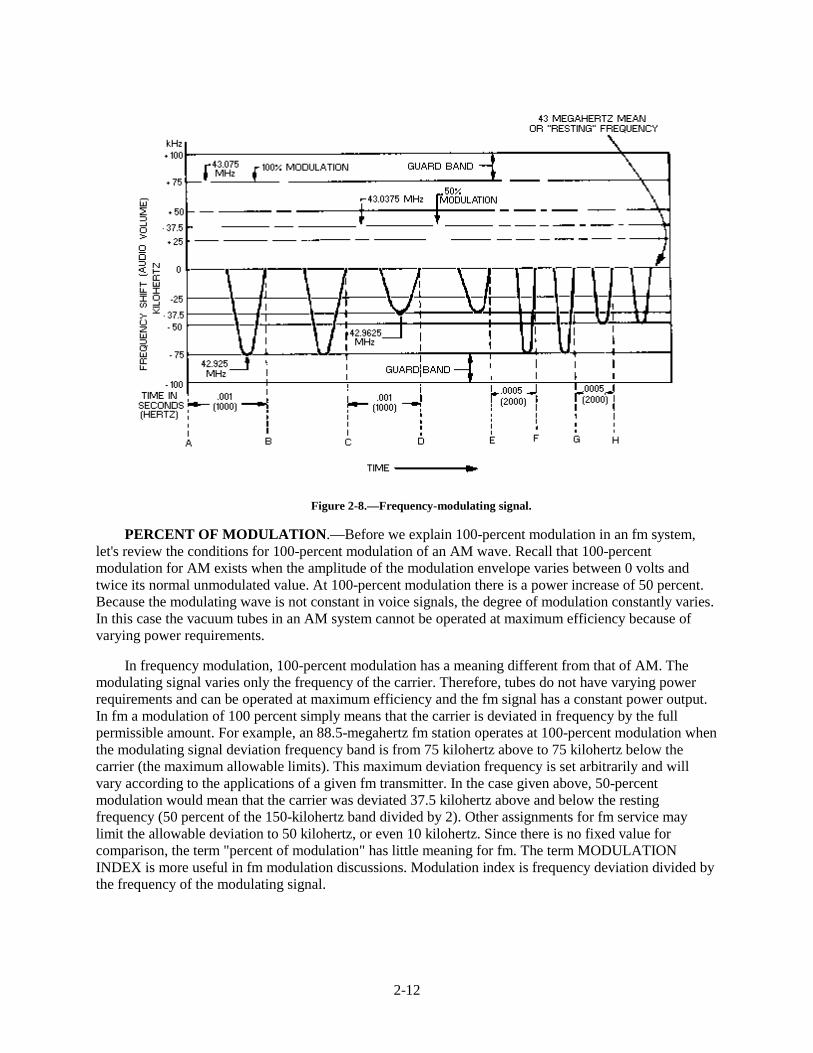
2-12
Figure 2-8.—Frequency-modulating signal.
PERCENT OF MODULATION.—Before we explain 100-percent modulation in an fm system,let's review the conditions for 100-percent modulation of an AM wave. Recall that 100-percentmodulation for AM exists when the amplitude of the modulation envelope varies between 0 volts andtwice its normal unmodulated value. At 100-percent modulation there is a power increase of 50 percent.Because the modulating wave is not constant in voice signals, the degree of modulation constantly varies.In this case the vacuum tubes in an AM system cannot be operated at maximum efficiency because ofvarying power requirements.
In frequency modulation, 100-percent modulation has a meaning different from that of AM. Themodulating signal varies only the frequency of the carrier. Therefore, tubes do not have varying powerrequirements and can be operated at maximum efficiency and the fm signal has a constant power output.In fm a modulation of 100 percent simply means that the carrier is deviated in frequency by the fullpermissible amount. For example, an 88.5-megahertz fm station operates at 100-percent modulation whenthe modulating signal deviation frequency band is from 75 kilohertz above to 75 kilohertz below thecarrier (the maximum allowable limits). This maximum deviation frequency is set arbitrarily and willvary according to the applications of a given fm transmitter. In the case given above, 50-percentmodulation would mean that the carrier was deviated 37.5 kilohertz above and below the restingfrequency (50 percent of the 150-kilohertz band divided by 2). Other assignments for fm service maylimit the allowable deviation to 50 kilohertz, or even 10 kilohertz. Since there is no fixed value forcomparison, the term "percent of modulation" has little meaning for fm. The term MODULATIONINDEX is more useful in fm modulation discussions. Modulation index is frequency deviation divided bythe frequency of the modulating signal.

2-13
MODULATION INDEX.—This ratio of frequency deviation to frequency of the modulating signalis useful because it also describes the ratio of amplitude to tone for the audio signal. These factorsdetermine the number and spacing of the side frequencies of the transmitted signal. The modulation indexformula is shown below:
Views (A) and (B) of figure 2-9 show the frequency spectrum for various fm signals. In the fourexamples of view (A), the modulating frequency is constant; the deviation frequency is changed to showthe effects of modulation indexes of 0.5, 1.0, 5.0, and 10.0. In view (B) the deviation frequency is heldconstant and the modulating frequency is varied to give the same modulation indexes.
Figure 2-9.—Frequency spectra of fm waves under various conditions.
You can determine several facts about fm signals by studying the frequency spectrum. For example,table 2-1 was developed from the information in figure 2-9. Notice in the top spectrums of both views (A)and (B) that the modulation index is 0.5. Also notice as you look at the next lower spectrums that themodulation index is 1.0. Next down is 5.0, and finally, the bottom spectrums have modulation indexes of
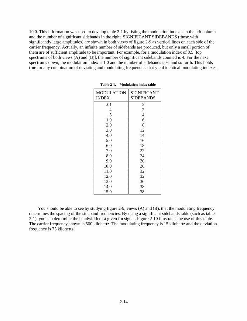
2-14
10.0. This information was used to develop table 2-1 by listing the modulation indexes in the left columnand the number of significant sidebands in the right. SIGNIFICANT SIDEBANDS (those withsignificantly large amplitudes) are shown in both views of figure 2-9 as vertical lines on each side of thecarrier frequency. Actually, an infinite number of sidebands are produced, but only a small portion ofthem are of sufficient amplitude to be important. For example, for a modulation index of 0.5 [topspectrums of both views (A) and (B)], the number of significant sidebands counted is 4. For the nextspectrums down, the modulation index is 1.0 and the number of sidebands is 6, and so forth. This holdstrue for any combination of deviating and modulating frequencies that yield identical modulating indexes.
Table 2-1.—Modulation index table
MODULATIONINDEX
SIGNIFICANTSIDEBANDS
.01 2.4 2.5 4
1.0 62.0 83.0 124.0 145.0 166.0 187.0 228.0 249.0 26
10.0 2811.0 3212.0 3213.0 3614.0 3815.0 38
You should be able to see by studying figure 2-9, views (A) and (B), that the modulating frequencydetermines the spacing of the sideband frequencies. By using a significant sidebands table (such as table2-1), you can determine the bandwidth of a given fm signal. Figure 2-10 illustrates the use of this table.The carrier frequency shown is 500 kilohertz. The modulating frequency is 15 kilohertz and the deviationfrequency is 75 kilohertz.
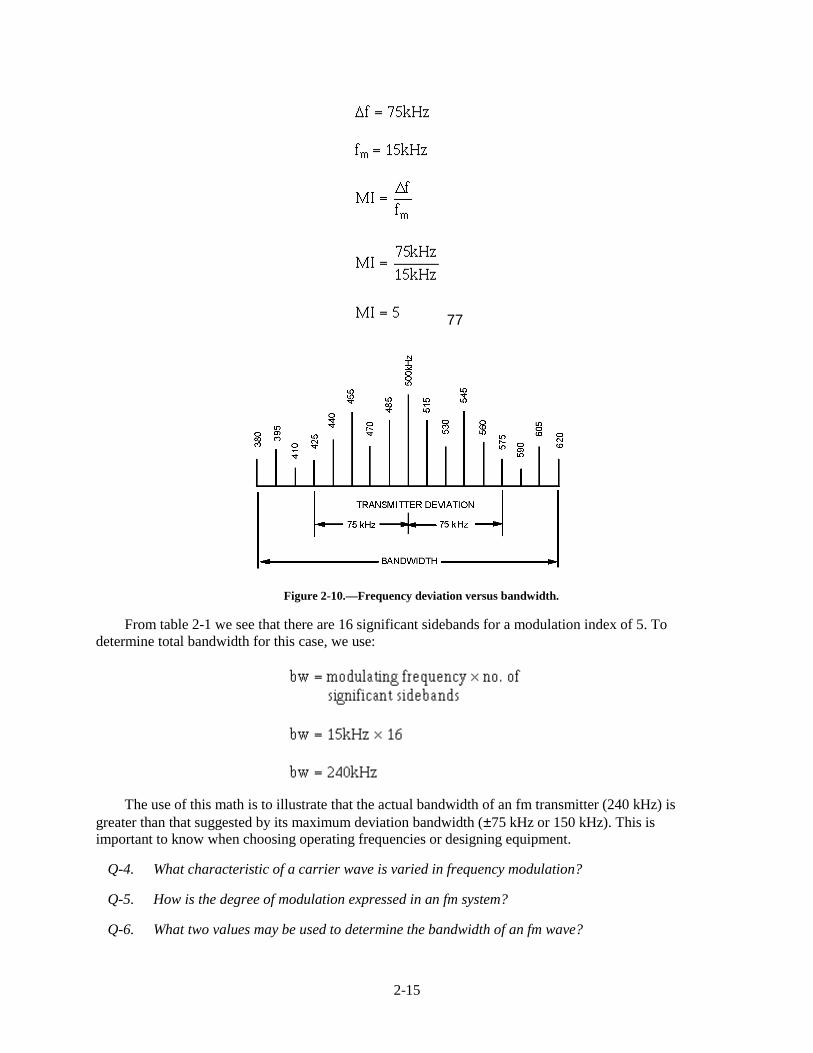
2-15
77
Figure 2-10.—Frequency deviation versus bandwidth.
From table 2-1 we see that there are 16 significant sidebands for a modulation index of 5. Todetermine total bandwidth for this case, we use:
The use of this math is to illustrate that the actual bandwidth of an fm transmitter (240 kHz) isgreater than that suggested by its maximum deviation bandwidth (±75 kHz or 150 kHz). This isimportant to know when choosing operating frequencies or designing equipment.
Q-4. What characteristic of a carrier wave is varied in frequency modulation?
Q-5. How is the degree of modulation expressed in an fm system?
Q-6. What two values may be used to determine the bandwidth of an fm wave?
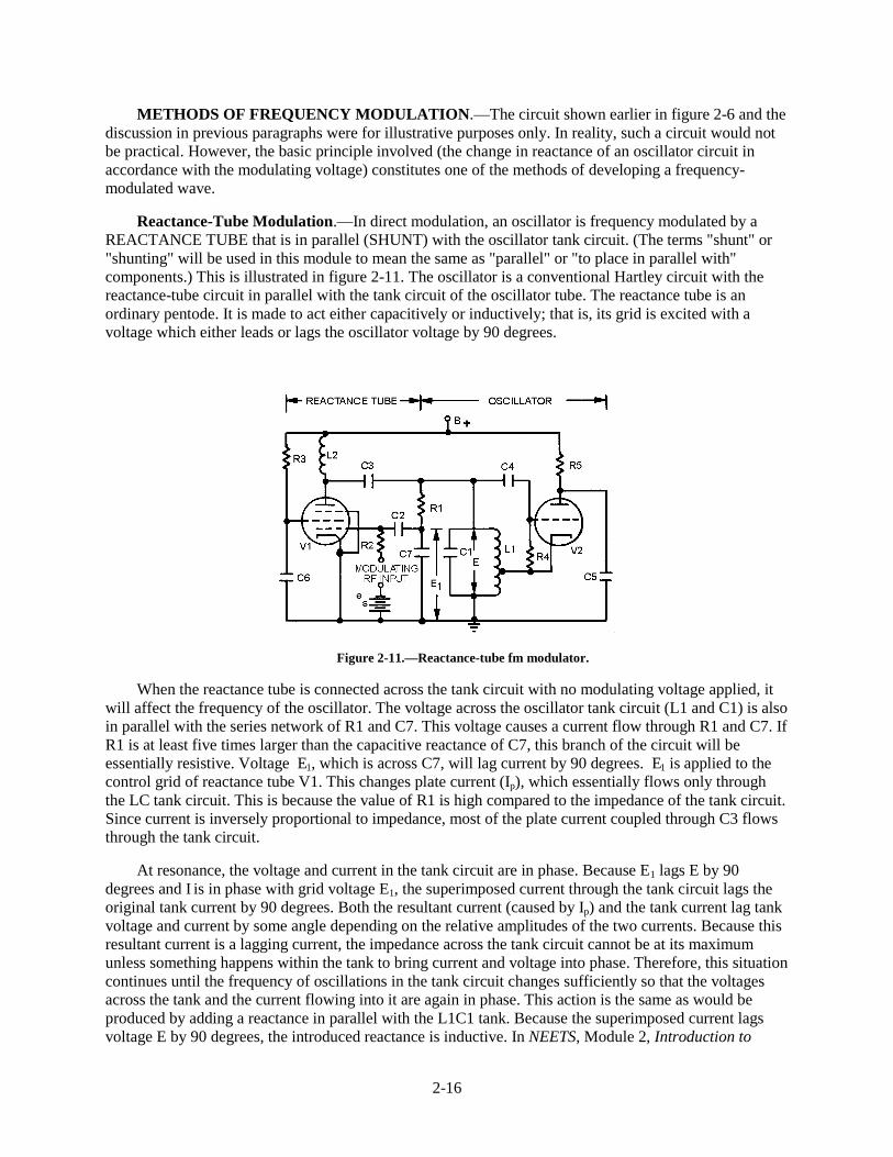
2-16
METHODS OF FREQUENCY MODULATION.—The circuit shown earlier in figure 2-6 and thediscussion in previous paragraphs were for illustrative purposes only. In reality, such a circuit would notbe practical. However, the basic principle involved (the change in reactance of an oscillator circuit inaccordance with the modulating voltage) constitutes one of the methods of developing a frequency-modulated wave.
Reactance-Tube Modulation.—In direct modulation, an oscillator is frequency modulated by aREACTANCE TUBE that is in parallel (SHUNT) with the oscillator tank circuit. (The terms "shunt" or"shunting" will be used in this module to mean the same as "parallel" or "to place in parallel with"components.) This is illustrated in figure 2-11. The oscillator is a conventional Hartley circuit with thereactance-tube circuit in parallel with the tank circuit of the oscillator tube. The reactance tube is anordinary pentode. It is made to act either capacitively or inductively; that is, its grid is excited with avoltage which either leads or lags the oscillator voltage by 90 degrees.
Figure 2-11.—Reactance-tube fm modulator.
When the reactance tube is connected across the tank circuit with no modulating voltage applied, itwill affect the frequency of the oscillator. The voltage across the oscillator tank circuit (L1 and C1) is alsoin parallel with the series network of R1 and C7. This voltage causes a current flow through R1 and C7. IfR1 is at least five times larger than the capacitive reactance of C7, this branch of the circuit will beessentially resistive. Voltage E 1, which is across C7, will lag current by 90 degrees. E 1 is applied to thecontrol grid of reactance tube V1. This changes plate current (Ip), which essentially flows only throughthe LC tank circuit. This is because the value of R1 is high compared to the impedance of the tank circuit.Since current is inversely proportional to impedance, most of the plate current coupled through C3 flowsthrough the tank circuit.
At resonance, the voltage and current in the tank circuit are in phase. Because E1 lags E by 90degrees and I is in phase with grid voltage E1, the superimposed current through the tank circuit lags theoriginal tank current by 90 degrees. Both the resultant current (caused by Ip) and the tank current lag tankvoltage and current by some angle depending on the relative amplitudes of the two currents. Because thisresultant current is a lagging current, the impedance across the tank circuit cannot be at its maximumunless something happens within the tank to bring current and voltage into phase. Therefore, this situationcontinues until the frequency of oscillations in the tank circuit changes sufficiently so that the voltagesacross the tank and the current flowing into it are again in phase. This action is the same as would beproduced by adding a reactance in parallel with the L1C1 tank. Because the superimposed current lagsvoltage E by 90 degrees, the introduced reactance is inductive. In NEETS, Module 2, Introduction to
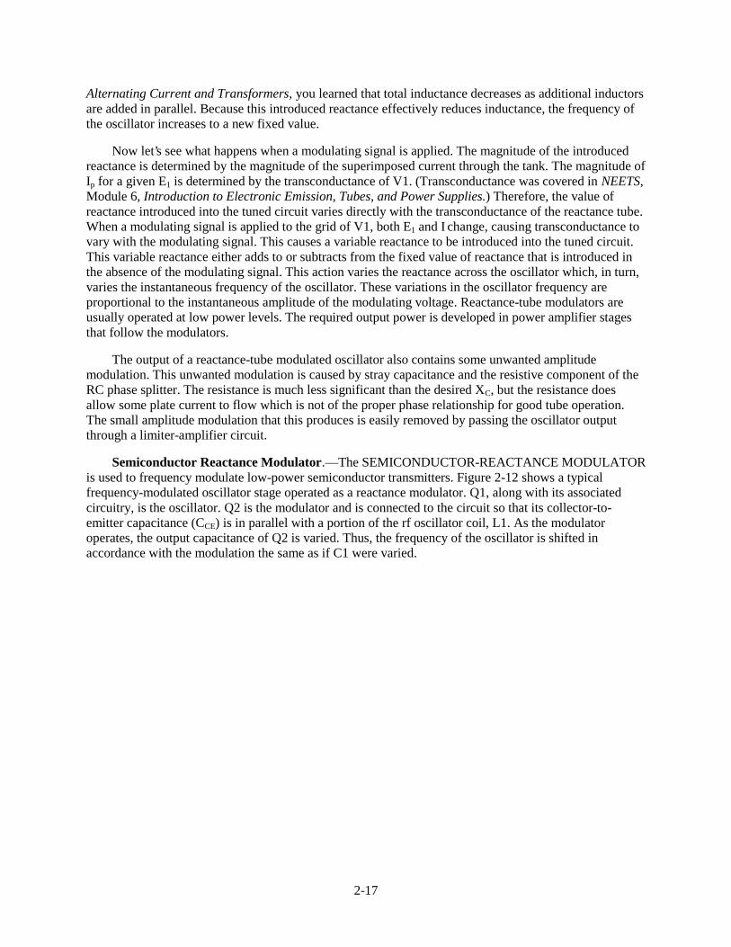
2-17
Alternating Current and Transformers, you learned that total inductance decreases as additional inductorsare added in parallel. Because this introduced reactance effectively reduces inductance, the frequency ofthe oscillator increases to a new fixed value.
Now let’s see what happens when a modulating signal is applied. The magnitude of the introducedreactance is determined by the magnitude of the superimposed current through the tank. The magnitude ofIp for a given E1 is determined by the transconductance of V1. (Transconductance was covered in NEETS,Module 6, Introduction to Electronic Emission, Tubes, and Power Supplies.) Therefore, the value ofreactance introduced into the tuned circuit varies directly with the transconductance of the reactance tube.When a modulating signal is applied to the grid of V1, both E1 and I change, causing transconductance tovary with the modulating signal. This causes a variable reactance to be introduced into the tuned circuit.This variable reactance either adds to or subtracts from the fixed value of reactance that is introduced inthe absence of the modulating signal. This action varies the reactance across the oscillator which, in turn,varies the instantaneous frequency of the oscillator. These variations in the oscillator frequency areproportional to the instantaneous amplitude of the modulating voltage. Reactance-tube modulators areusually operated at low power levels. The required output power is developed in power amplifier stagesthat follow the modulators.
The output of a reactance-tube modulated oscillator also contains some unwanted amplitudemodulation. This unwanted modulation is caused by stray capacitance and the resistive component of theRC phase splitter. The resistance is much less significant than the desired XC, but the resistance doesallow some plate current to flow which is not of the proper phase relationship for good tube operation.The small amplitude modulation that this produces is easily removed by passing the oscillator outputthrough a limiter-amplifier circuit.
Semiconductor Reactance Modulator.—The SEMICONDUCTOR-REACTANCE MODULATORis used to frequency modulate low-power semiconductor transmitters. Figure 2-12 shows a typicalfrequency-modulated oscillator stage operated as a reactance modulator. Q1, along with its associatedcircuitry, is the oscillator. Q2 is the modulator and is connected to the circuit so that its collector-to-emitter capacitance (CCE) is in parallel with a portion of the rf oscillator coil, L1. As the modulatoroperates, the output capacitance of Q2 is varied. Thus, the frequency of the oscillator is shifted inaccordance with the modulation the same as if C1 were varied.
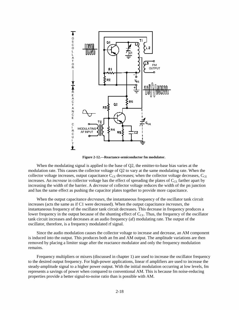
2-18
Figure 2-12.—Reactance-semiconductor fm modulator.
When the modulating signal is applied to the base of Q2, the emitter-to-base bias varies at themodulation rate. This causes the collector voltage of Q2 to vary at the same modulating rate. When thecollector voltage increases, output capacitance CCE decreases; when the collector voltage decreases, CCE
increases. An increase in collector voltage has the effect of spreading the plates of CCE farther apart byincreasing the width of the barrier. A decrease of collector voltage reduces the width of the pn junctionand has the same effect as pushing the capacitor plates together to provide more capacitance.
When the output capacitance decreases, the instantaneous frequency of the oscillator tank circuitincreases (acts the same as if C1 were decreased). When the output capacitance increases, theinstantaneous frequency of the oscillator tank circuit decreases. This decrease in frequency produces alower frequency in the output because of the shunting effect of CCE. Thus, the frequency of the oscillatortank circuit increases and decreases at an audio frequency (af) modulating rate. The output of theoscillator, therefore, is a frequency modulated rf signal.
Since the audio modulation causes the collector voltage to increase and decrease, an AM componentis induced into the output. This produces both an fm and AM output. The amplitude variations are thenremoved by placing a limiter stage after the reactance modulator and only the frequency modulationremains.
Frequency multipliers or mixers (discussed in chapter 1) are used to increase the oscillator frequencyto the desired output frequency. For high-power applications, linear rf amplifiers are used to increase thesteady-amplitude signal to a higher power output. With the initial modulation occurring at low levels, fmrepresents a savings of power when compared to conventional AM. This is because fm noise-reducingproperties provide a better signal-to-noise ratio than is possible with AM.

2-19
Multivibrator Modulator.—Another type of frequency modulator is the astable multivibratorillustrated in figure 2-13. Inserting the modulating af voltage in series with the base-return of themultivibrator transistors causes the gate length, and thus the fundamental frequency of the multivibrator,to vary. The amount of variation will be in accordance with the amplitude of the modulating voltage. Onerequirement of this method is that the fundamental frequency of the multivibrator be high in relation tothe highest modulating frequencies. A factor of at least 100 provides the best results.
Figure 2-13.—Astable multivibrator and filter circuit for generating an fm carrier.
Recall that a multivibrator output consists of the fundamental frequency and all of its harmonics.Unwanted even harmonics are eliminated by using a SYMMETRICAL MULTIVIBRATOR circuit, asshown in figure 2-13. The desired fundamental frequency, or desired odd harmonics, can be amplifiedafter all other odd harmonics are eliminated in the LCR filter section of figure 2-13. A single frequency-modulated carrier is then made available for further amplification and transmission.
Proper design of the multivibrator will cause the frequency deviation of the carrier to faithfullyfollow (referred to as a "linear" function) the modulating voltage. This is true up to frequency deviationswhich are considerable fractions of the fundamental frequency of the multivibrator. The principal designconsideration is that the RC coupling from one multivibrator transistor base to the collector of the otherhas a time constant which is greater than the actual gate length by a factor of 10 or more. Under theseconditions, a rise in base voltage in each transistor is essentially linear from cutoff to the bias at which thetransistor is switched on. Since this rise in base voltage is a linear function of time, the gate length willchange as an inverse function of the modulating voltage. This action will cause the frequency to change asa linear function of the modulating voltage.
The multivibrator frequency modulator has the advantage over the reactance-type modulator of agreater linear frequency deviation from a given carrier frequency. However, multivibrators are limited tofrequencies below about 1 megahertz. Both systems are subject to drift of the carrier frequency and must,therefore, be stabilized. Stabilization may be accomplished by modulating at a relatively low frequencyand translating by heterodyne action to the desired output frequency, as shown in figure 2-14. A1-megahertz signal is heterodyned with 49 megahertz from the crystal-controlled oscillator to provide astable 50-megahertz output from the mixer. If a suitably stable heterodyning oscillator is used, thefrequency stability can be greatly improved. For instance, at the frequencies shown in figure 2-14, the
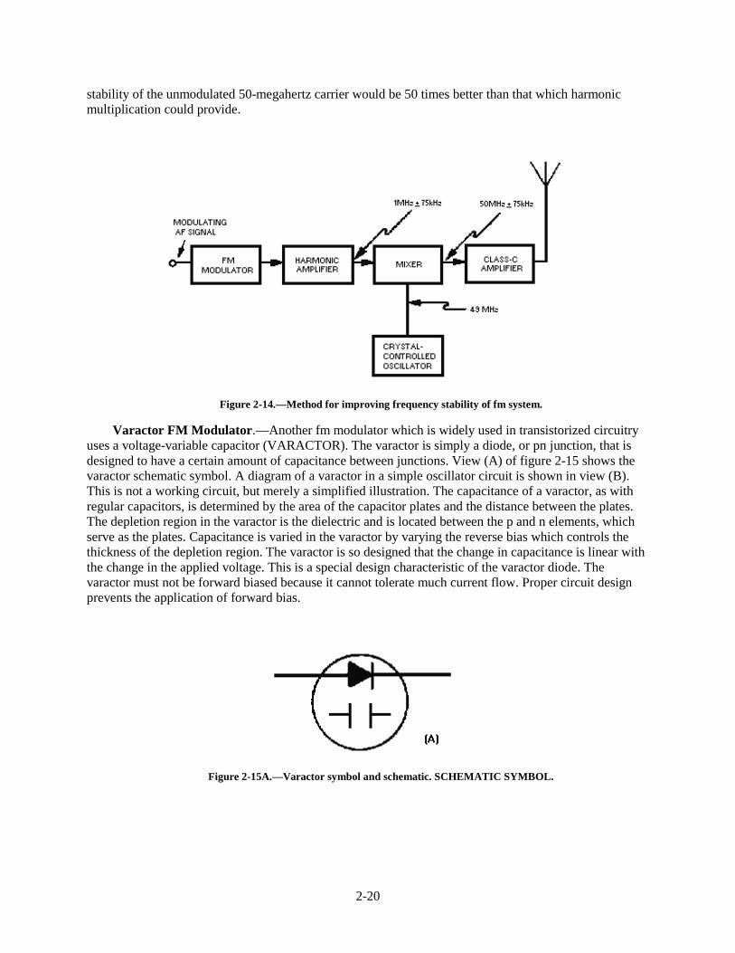
2-20
stability of the unmodulated 50-megahertz carrier would be 50 times better than that which harmonicmultiplication could provide.
Figure 2-14.—Method for improving frequency stability of fm system.
Varactor FM Modulator.—Another fm modulator which is widely used in transistorized circuitryuses a voltage-variable capacitor (VARACTOR). The varactor is simply a diode, or pn junction, that isdesigned to have a certain amount of capacitance between junctions. View (A) of figure 2-15 shows thevaractor schematic symbol. A diagram of a varactor in a simple oscillator circuit is shown in view (B).This is not a working circuit, but merely a simplified illustration. The capacitance of a varactor, as withregular capacitors, is determined by the area of the capacitor plates and the distance between the plates.The depletion region in the varactor is the dielectric and is located between the p and n elements, whichserve as the plates. Capacitance is varied in the varactor by varying the reverse bias which controls thethickness of the depletion region. The varactor is so designed that the change in capacitance is linear withthe change in the applied voltage. This is a special design characteristic of the varactor diode. Thevaractor must not be forward biased because it cannot tolerate much current flow. Proper circuit designprevents the application of forward bias.
Figure 2-15A.—Varactor symbol and schematic. SCHEMATIC SYMBOL.

2-21
Figure 2-15B.—Varactor symbol and schematic. SIMPLIFIED CIRCUIT.
Notice the simplicity of operation of the circuit in figure 2-16. An af signal that is applied to theinput results in the following actions: (1) On the positive alternation, reverse bias increases and thedielectric (depletion region) width increases. This decreases capacitance which increases the frequency ofthe oscillator. (2) On the negative alternation, the reverse bias decreases, which results in a decrease inoscillator frequency.
Figure 2-16.—Varactor fm modulator.
Many different fm modulators are available, but they all use the basic principles you have juststudied. The main point to remember is that an oscillator must be used to establish the reference (carrier)frequency. Secondly, some method is needed to cause the oscillator to change frequency in accordancewith an af signal. Anytime this can be accomplished, we have a frequency modulator.
Q-7. How does the reactance-tube modulator impress intelligence onto an rf carrier?
Q-8. What characteristic of a transistor is varied in a semiconductor-reactance modulator?
Q-9. What circuit section is required in the output of a multivibrator modulator to eliminateunwanted output frequencies?
Q-10. What characteristic of a varactor is used in an fm modulator?
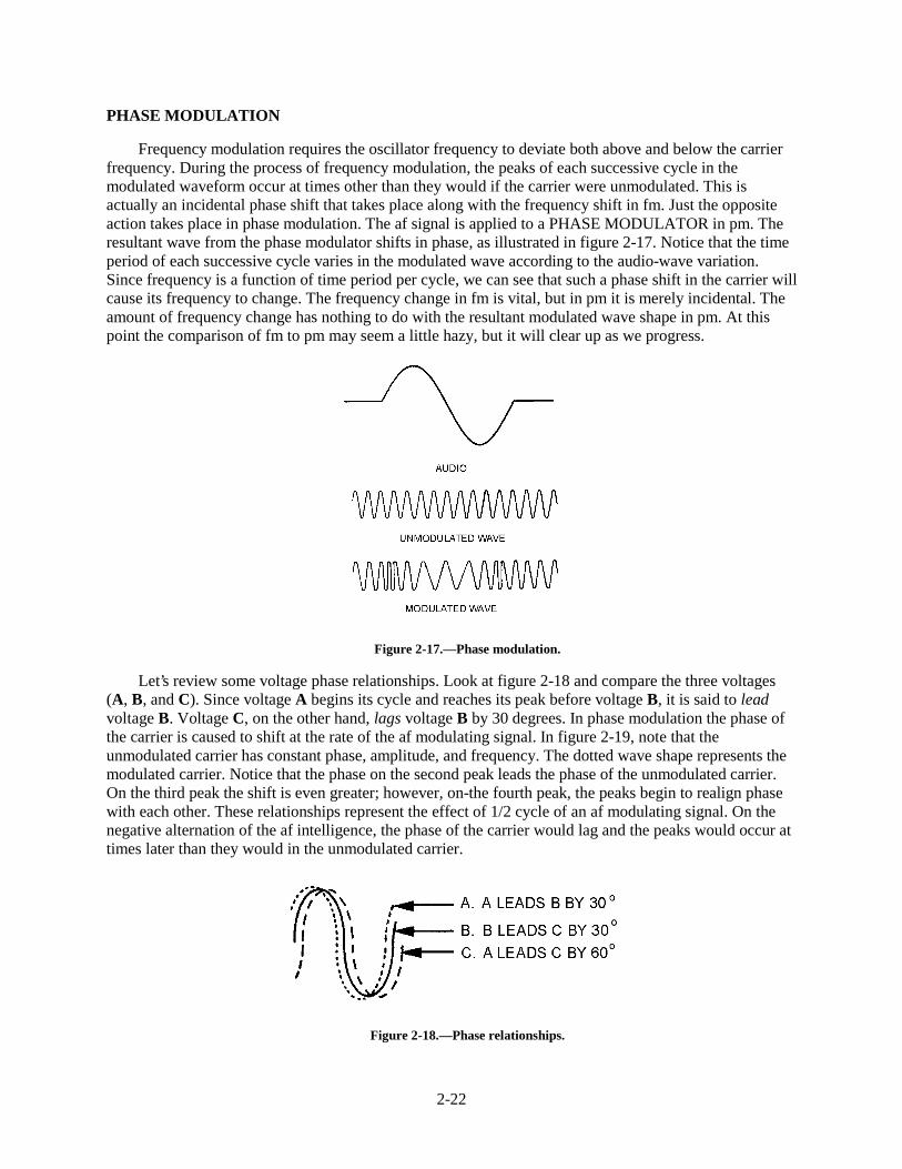
2-22
PHASE MODULATION
Frequency modulation requires the oscillator frequency to deviate both above and below the carrierfrequency. During the process of frequency modulation, the peaks of each successive cycle in themodulated waveform occur at times other than they would if the carrier were unmodulated. This isactually an incidental phase shift that takes place along with the frequency shift in fm. Just the oppositeaction takes place in phase modulation. The af signal is applied to a PHASE MODULATOR in pm. Theresultant wave from the phase modulator shifts in phase, as illustrated in figure 2-17. Notice that the timeperiod of each successive cycle varies in the modulated wave according to the audio-wave variation.Since frequency is a function of time period per cycle, we can see that such a phase shift in the carrier willcause its frequency to change. The frequency change in fm is vital, but in pm it is merely incidental. Theamount of frequency change has nothing to do with the resultant modulated wave shape in pm. At thispoint the comparison of fm to pm may seem a little hazy, but it will clear up as we progress.
Figure 2-17.—Phase modulation.
Let’s review some voltage phase relationships. Look at figure 2-18 and compare the three voltages(A, B, and C). Since voltage A begins its cycle and reaches its peak before voltage B, it is said to leadvoltage B. Voltage C, on the other hand, lags voltage B by 30 degrees. In phase modulation the phase ofthe carrier is caused to shift at the rate of the af modulating signal. In figure 2-19, note that theunmodulated carrier has constant phase, amplitude, and frequency. The dotted wave shape represents themodulated carrier. Notice that the phase on the second peak leads the phase of the unmodulated carrier.On the third peak the shift is even greater; however, on-the fourth peak, the peaks begin to realign phasewith each other. These relationships represent the effect of 1/2 cycle of an af modulating signal. On thenegative alternation of the af intelligence, the phase of the carrier would lag and the peaks would occur attimes later than they would in the unmodulated carrier.
Figure 2-18.—Phase relationships.
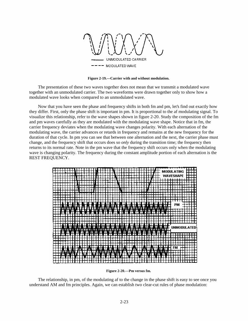
2-23
Figure 2-19.—Carrier with and without modulation.
The presentation of these two waves together does not mean that we transmit a modulated wavetogether with an unmodulated carrier. The two waveforms were drawn together only to show how amodulated wave looks when compared to an unmodulated wave.
Now that you have seen the phase and frequency shifts in both fm and pm, let’s find out exactly howthey differ. First, only the phase shift is important in pm. It is proportional to the af modulating signal. Tovisualize this relationship, refer to the wave shapes shown in figure 2-20. Study the composition of the fmand pm waves carefully as they are modulated with the modulating wave shape. Notice that in fm, thecarrier frequency deviates when the modulating wave changes polarity. With each alternation of themodulating wave, the carrier advances or retards in frequency and remains at the new frequency for theduration of that cycle. In pm you can see that between one alternation and the next, the carrier phase mustchange, and the frequency shift that occurs does so only during the transition time; the frequency thenreturns to its normal rate. Note in the pm wave that the frequency shift occurs only when the modulatingwave is changing polarity. The frequency during the constant amplitude portion of each alternation is theREST FREQUENCY.
Figure 2-20.—Pm versus fm.
The relationship, in pm, of the modulating af to the change in the phase shift is easy to see once youunderstand AM and fm principles. Again, we can establish two clear-cut rules of phase modulation:
2-24
• AMOUNT OF PHASE SHIFT IS PROPORTIONAL TO THE AMPLITUDE OF THEMODULATING SIGNAL.
(If a 10-volt signal causes a phase shift of 20 degrees, then a 20-volt signal causes a phase shift of 40degrees.)
• RATE OF PHASE SHIFT IS PROPORTIONAL TO THE FREQUENCY OF THEMODULATING SIGNAL.
(If the carrier were modulated with a 1-kilohertz tone, the carrier would advance and retard in phase1,000 times each second.)
Phase modulation is also similar to frequency modulation in the number of sidebands that existwithin the modulated wave and the spacing between sidebands. Phase modulation will also produce aninfinite number of sideband frequencies. The spacing between these sidebands will be equal to thefrequency of the modulating signal. However, one factor is very different in phase modulation; that is, thedistribution of power in pm sidebands is not similar to that in fm sidebands, as will be explained in thenext section.
Modulation Index
Recall from frequency modulation that modulation index is used to calculate the number ofsignificant sidebands existing in the waveform. The higher the modulation index, the greater the numberof sideband pairs. The modulation index is the ratio between the amount of oscillator deviation and thefrequency of the modulating signal:
In frequency modulation, we saw that as the frequency of the modulating signal increased (assumingthe deviation remained constant) the number of significant sideband pairs decreased. This is shown inviews (A) and (B) of figure 2-21. Notice that although the total number of significant sidebands decreaseswith a higher frequency-modulating signal, the sidebands spread out relative to each other; the totalbandwidth increases.

2-25
Figure 2-21.—Fm versus pm spectrum distribution.
In phase modulation the oscillator does not deviate, and the power in the sidebands is a function ofthe amplitude of the modulating signal. Therefore, two signals, one at 5 kilohertz and the other at 10kilohertz, used to modulate a carrier would have the same sideband power distribution. However, the10-kilohertz sidebands would be farther apart, as shown in views (C) and (D) of figure 2-21. Whencompared to fm, the bandwidth of the pm transmitted signal is greatly increased as the frequency of themodulating signal is increased.
As we pointed out earlier, phase modulation cannot occur without an incidental change in frequency,nor can frequency modulation occur without an incidental change in phase. The term fm is loosely usedwhen referring to any type of angle modulation, and phase modulation is sometimes incorrectly referredto as "indirect fm." This is a definition that you should disregard to avoid confusion. Phase modulation isjust what the words imply — phase modulation of a carrier by an af modulating signal. You will developa better understanding of these points as you advance in your study of modulation.
Basic Modulator
In phase modulation you learned that varying the phase of a carrier at an intelligence rate caused thatcarrier to contain variations which could be converted back into intelligence. One circuit that can causethis phase variation is shown in figure 2-22.
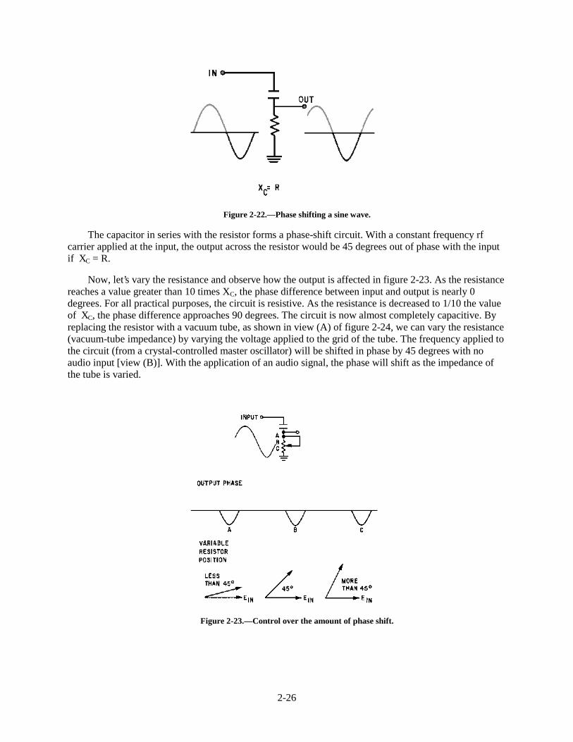
2-26
Figure 2-22.—Phase shifting a sine wave.
The capacitor in series with the resistor forms a phase-shift circuit. With a constant frequency rfcarrier applied at the input, the output across the resistor would be 45 degrees out of phase with the inputif X C = R.
Now, let’s vary the resistance and observe how the output is affected in figure 2-23. As the resistancereaches a value greater than 10 times XC, the phase difference between input and output is nearly 0degrees. For all practical purposes, the circuit is resistive. As the resistance is decreased to 1/10 the valueof X C, the phase difference approaches 90 degrees. The circuit is now almost completely capacitive. Byreplacing the resistor with a vacuum tube, as shown in view (A) of figure 2-24, we can vary the resistance(vacuum-tube impedance) by varying the voltage applied to the grid of the tube. The frequency applied tothe circuit (from a crystal-controlled master oscillator) will be shifted in phase by 45 degrees with noaudio input [view (B)]. With the application of an audio signal, the phase will shift as the impedance ofthe tube is varied.
Figure 2-23.—Control over the amount of phase shift.
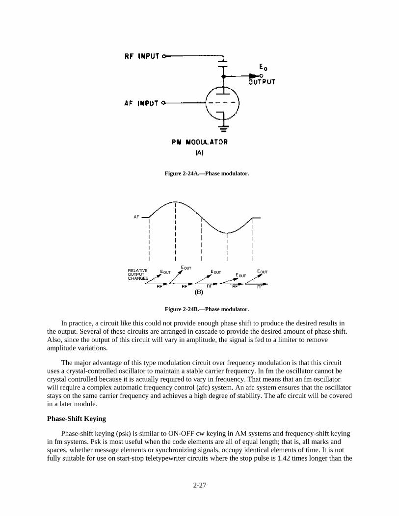
2-27
Figure 2-24A.—Phase modulator.
Figure 2-24B.—Phase modulator.
In practice, a circuit like this could not provide enough phase shift to produce the desired results inthe output. Several of these circuits are arranged in cascade to provide the desired amount of phase shift.Also, since the output of this circuit will vary in amplitude, the signal is fed to a limiter to removeamplitude variations.
The major advantage of this type modulation circuit over frequency modulation is that this circuituses a crystal-controlled oscillator to maintain a stable carrier frequency. In fm the oscillator cannot becrystal controlled because it is actually required to vary in frequency. That means that an fm oscillatorwill require a complex automatic frequency control (afc) system. An afc system ensures that the oscillatorstays on the same carrier frequency and achieves a high degree of stability. The afc circuit will be coveredin a later module.
Phase-Shift Keying
Phase-shift keying (psk) is similar to ON-OFF cw keying in AM systems and frequency-shift keyingin fm systems. Psk is most useful when the code elements are all of equal length; that is, all marks andspaces, whether message elements or synchronizing signals, occupy identical elements of time. It is notfully suitable for use on start-stop teletypewriter circuits where the stop pulse is 1.42 times longer than the
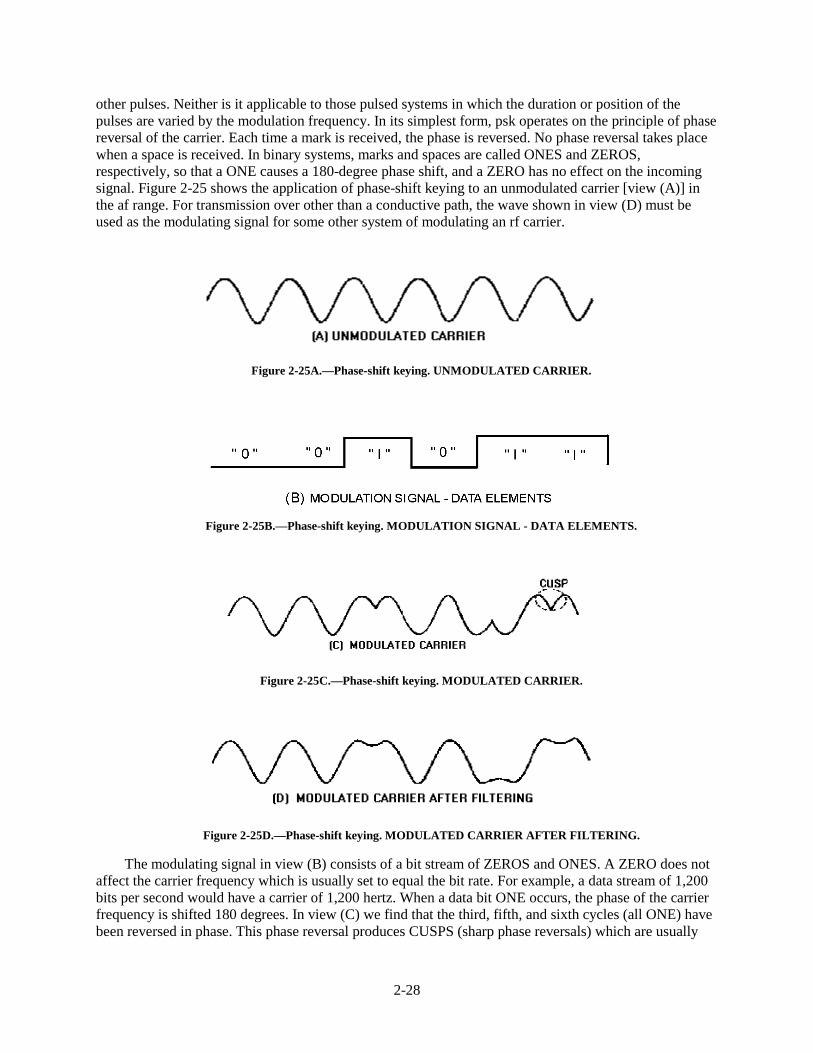
2-28
other pulses. Neither is it applicable to those pulsed systems in which the duration or position of thepulses are varied by the modulation frequency. In its simplest form, psk operates on the principle of phasereversal of the carrier. Each time a mark is received, the phase is reversed. No phase reversal takes placewhen a space is received. In binary systems, marks and spaces are called ONES and ZEROS,respectively, so that a ONE causes a 180-degree phase shift, and a ZERO has no effect on the incomingsignal. Figure 2-25 shows the application of phase-shift keying to an unmodulated carrier [view (A)] inthe af range. For transmission over other than a conductive path, the wave shown in view (D) must beused as the modulating signal for some other system of modulating an rf carrier.
Figure 2-25A.—Phase-shift keying. UNMODULATED CARRIER.
Figure 2-25B.—Phase-shift keying. MODULATION SIGNAL - DATA ELEMENTS.
Figure 2-25C.—Phase-shift keying. MODULATED CARRIER.
Figure 2-25D.—Phase-shift keying. MODULATED CARRIER AFTER FILTERING.
The modulating signal in view (B) consists of a bit stream of ZEROS and ONES. A ZERO does notaffect the carrier frequency which is usually set to equal the bit rate. For example, a data stream of 1,200bits per second would have a carrier of 1,200 hertz. When a data bit ONE occurs, the phase of the carrierfrequency is shifted 180 degrees. In view (C) we find that the third, fifth, and sixth cycles (all ONE) havebeen reversed in phase. This phase reversal produces CUSPS (sharp phase reversals) which are usually
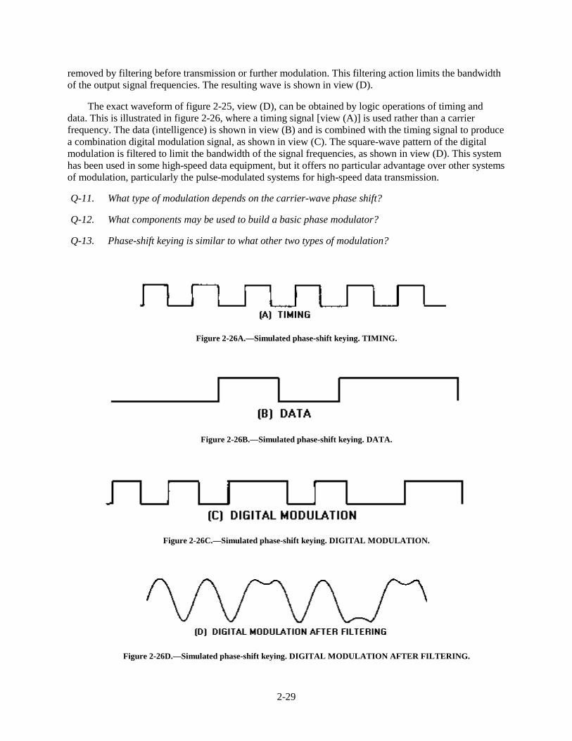
2-29
removed by filtering before transmission or further modulation. This filtering action limits the bandwidthof the output signal frequencies. The resulting wave is shown in view (D).
The exact waveform of figure 2-25, view (D), can be obtained by logic operations of timing anddata. This is illustrated in figure 2-26, where a timing signal [view (A)] is used rather than a carrierfrequency. The data (intelligence) is shown in view (B) and is combined with the timing signal to producea combination digital modulation signal, as shown in view (C). The square-wave pattern of the digitalmodulation is filtered to limit the bandwidth of the signal frequencies, as shown in view (D). This systemhas been used in some high-speed data equipment, but it offers no particular advantage over other systemsof modulation, particularly the pulse-modulated systems for high-speed data transmission.
Q-11. What type of modulation depends on the carrier-wave phase shift?
Q-12. What components may be used to build a basic phase modulator?
Q-13. Phase-shift keying is similar to what other two types of modulation?
Figure 2-26A.—Simulated phase-shift keying. TIMING.
Figure 2-26B.—Simulated phase-shift keying. DATA.
Figure 2-26C.—Simulated phase-shift keying. DIGITAL MODULATION.
Figure 2-26D.—Simulated phase-shift keying. DIGITAL MODULATION AFTER FILTERING.
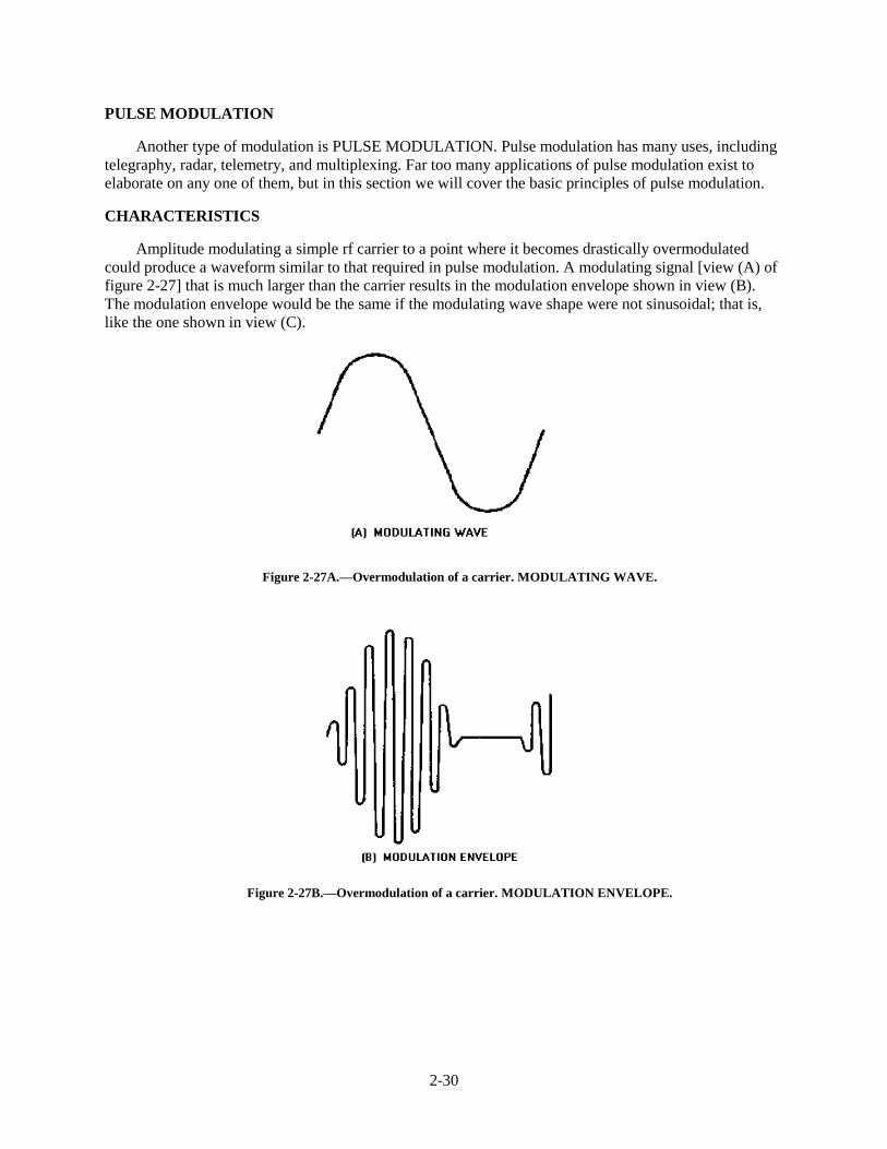
2-30
PULSE MODULATION
Another type of modulation is PULSE MODULATION. Pulse modulation has many uses, includingtelegraphy, radar, telemetry, and multiplexing. Far too many applications of pulse modulation exist toelaborate on any one of them, but in this section we will cover the basic principles of pulse modulation.
CHARACTERISTICS
Amplitude modulating a simple rf carrier to a point where it becomes drastically overmodulatedcould produce a waveform similar to that required in pulse modulation. A modulating signal [view (A) offigure 2-27] that is much larger than the carrier results in the modulation envelope shown in view (B).The modulation envelope would be the same if the modulating wave shape were not sinusoidal; that is,like the one shown in view (C).
Figure 2-27A.—Overmodulation of a carrier. MODULATING WAVE.
Figure 2-27B.—Overmodulation of a carrier. MODULATION ENVELOPE.
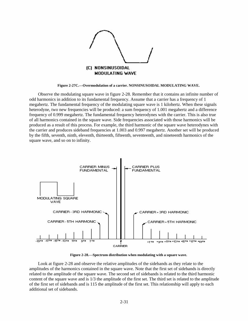
2-31
Figure 2-27C.—Overmodulation of a carrier. NONSINUSOIDAL MODULATING WAVE.
Observe the modulating square wave in figure 2-28. Remember that it contains an infinite number ofodd harmonics in addition to its fundamental frequency. Assume that a carrier has a frequency of 1megahertz. The fundamental frequency of the modulating square wave is 1 kilohertz. When these signalsheterodyne, two new frequencies will be produced: a sum frequency of 1.001 megahertz and a differencefrequency of 0.999 megahertz. The fundamental frequency heterodynes with the carrier. This is also trueof all harmonics contained in the square wave. Side frequencies associated with those harmonics will beproduced as a result of this process. For example, the third harmonic of the square wave heterodynes withthe carrier and produces sideband frequencies at 1.003 and 0.997 megahertz. Another set will be producedby the fifth, seventh, ninth, eleventh, thirteenth, fifteenth, seventeenth, and nineteenth harmonics of thesquare wave, and so on to infinity.
Figure 2-28.—Spectrum distribution when modulating with a square wave.
Look at figure 2-28 and observe the relative amplitudes of the sidebands as they relate to theamplitudes of the harmonics contained in the square wave. Note that the first set of sidebands is directlyrelated to the amplitude of the square wave. The second set of sidebands is related to the third harmoniccontent of the square wave and is 1/3 the amplitude of the first set. The third set is related to the amplitudeof the first set of sidebands and is 115 the amplitude of the first set. This relationship will apply to eachadditional set of sidebands.
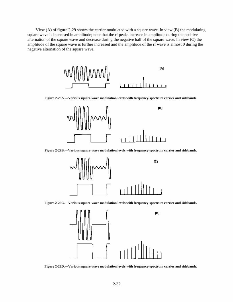
2-32
View (A) of figure 2-29 shows the carrier modulated with a square wave. In view (B) the modulatingsquare wave is increased in amplitude; note that the rf peaks increase in amplitude during the positivealternation of the square wave and decrease during the negative half of the square wave. In view (C) theamplitude of the square wave is further increased and the amplitude of the rf wave is almost 0 during thenegative alternation of the square wave.
Figure 2-29A.—Various square-wave modulation levels with frequency-spectrum carrier and sidebands.
Figure 2-29B.—Various square-wave modulation levels with frequency-spectrum carrier and sidebands.
Figure 2-29C.—Various square-wave modulation levels with frequency-spectrum carrier and sidebands.
Figure 2-29D.—Various square-wave modulation levels with frequency-spectrum carrier and sidebands.
2-33
Note the frequency spectrum associated with each of these conditions. The carrier amplitude remainsconstant, but the sidebands increase in amplitude in accordance with the amplitude of the modulatingsquare wave.
So far in pulse modulation, the same general rules apply as in AM. In view (C) the amplitude of thesquare wave of voltage is equal to the peak voltage of the unmodulated carrier wave. This is 100-percentmodulation, just as in conventional AM. Note in the frequency spectrum that the sideband distribution isalso the same as in AM. Keep in mind that the total sideband power is 1/2 of the total power when themodulator signal is a square wave. This is in contrast to 1/3 the total power with sine-wave modulation.
Now refer to view (D). The increase of the square-wave modulating voltage is greater in amplitudethan the unmodulated carrier. Notice that the sideband distribution does not change; but, as the sidebandstake on more of the transmitted power, so will the carrier.
Pulse Timing
Thus far, we have established a carrier and have caused its peaks to increase and decrease as amodulating square wave is applied. Some pulse-modulation systems modulate a carrier in this manner.Others produce no rf until pulsed; that is, rf occurs only during the actual pulse as shown in view (A) offigure 2-30. For example, let’s start with an rf carrier frequency of 1 megahertz. Each cycle of the rfrequires a certain amount of time to complete. If we allow oscillations to occur for a given period of timeonly during selected intervals, as in view (B), we are PULSING the system. Note that the pulsetransmitter does not produce an rf signal until one of the positive-going modulating pulses is applied. Thetransmitter then produces the rf carrier until the positive input pulse ends and the input waveform againbecomes a negative potential.
Figure 2-30A.—Pulse transmission.
Figure 2-30B.—Pulse transmission.
Refer back to figure 1-41 and the over-modulation discussion in chapter 1. You will notice that theovermodulation wave shape of view (D) in figure 2-29 and the pulse-modulation wave shape of figure2-30, view (B), are very similar to figure 1-41.
Actually, both figure 1-41 and view (D) of figure 2-29 result from overmodulation. Even though theoutput of the pulse transmitter in figure 2-30 looks like overmodulation, it is not; rather, it is pulsed.
2-34
However, the frequency spectrums are similar. Sideband distributions are similar, but not identical, sincethe pulse transmitter in figure 2-30 is gated on and off instead of being modulated by a square wave aswas the case in view (D) of figure 2-29.
Remember, in pulse modulation the sidebands produced to accompany the carrier duringtransmission are directly related to the harmonic content of the modulating wave shape. In figure 2-31,(view A, view B and view C), observe the square and rectangular wave shapes used to pulse modulate thesame carrier frequency in each of the three views.
Figure 2-31A.—Varying pulse-modulating waves.
Figure 2-31B.—Varying pulse-modulating waves.
Figure 2-31C.—Varying pulse-modulating waves.
Let’s take note of some timing relationships in the three modulating sequences in figure 2-31:
• the time for the rf cycle is the same in each case
• the number of cycles occurring in each group is different
• the ratio between transmitting and non-transmitting time varies
• the transmitter produces an rf wave four times in view (A), three transmission groups in view (B),and only two in view (C)
• rf is generated only during the positive pulses
2-35
In figure 2-32, observe the relative time for individual rf cycles. The time for each cycle is the samein views (A) and (B). Since this time is the same, we can assume that the carrier frequency is the same.But in view (C) the time for each cycle is about half that in views (A) and (B). Therefore, the frequencyof the carrier in view (C) is nearly twice that of the other two. This illustration shows that carrierfrequencies in pulse systems can vary.
Figure 2-32A.—Carrier frequency.
Figure 2-32B.—Carrier frequency.
Figure 2-32C.—Carrier frequency.
The carrier frequency is not the only frequency we must concern ourselves with in pulse systems.We must also be concerned with the frequency that is associated with the repetition rate of groups ofpulses. Figure 2-33 shows that a specific time period exists between each group of rf pulses. This time isthe same for each repetition of the pulse and is called the PULSE-REPETITION TIME (prt). To find outhow often these groups of pulses occur, compute PULSE-REPETITION FREQUENCY (prf) using theformula:
2-36
Figure 2-33.—Pulse-repetition time (prt).
Just remember that the pulse-repetition time is the time it takes for a pulse to recur, as shown infigure 2-34. The duration of time of the pulse (a) plus the time when no pulse occurs (b) equals the totalpulse-repetition time.
Figure 2-34.—Pulse cycles.
The time during which the pulse is occurring is called PULSE DURATION (pd) or PULSE WIDTH(pw), as shown in figure 2-35. As you will soon see, pulse width is important in pulse modulation.
Figure 2-35.—Pulse width (pw).

2-37
The time we have been referring to as the time of no pulse, or nonpulse time, is referred to as RESTTIME (rt). The duration of this rest time will determine certain capabilities of the pulse-modulationsystem. The pulse width is the time that the transmitter produces rf oscillations and is the actual pulsetransmission time. During the nonpulse time, shown in figure 2-36, the transmitter produces nooscillations and the oscillator is cut off.
Figure 2-36.—Rest time (rt).
Some pulse transmitter-receiver systems transmit the pulse and then rest, awaiting the return of anecho. Rest time provides the system time for the receive cycle of operation.
Power in a Pulse System
When discussing power in a pulse-modulation system, we have to consider PEAK POWER andAVERAGE POWER. Peak power is the maximum value of the transmitted pulse; average power is thepeak power value averaged over the pulse-repetition time. Peak power is very easy to see in a pulsesystem. In figure 2-37, all pulsed wave shapes have a peak power of 100 watts. Also note that in views(A), (B), and (C) the pulse width is the same, even though the carrier frequency is different. In these threecases average power would be the same. This is because average power is actually equal to the peakpower of a pulse averaged over 1 operating cycle. However, the pulse width is increased in view (D) andwe have a greater average power with the same prt. In view (E) the decreased pulse width has decreasedaverage power over the same prt.
Figure 2-37.—Peak and average power.
2-38
Use these simple rules to determine power in a pulsed-wave shape:
• Peak power is the maximum power reached by the transmitter during the pulse.
• Average power equals the peak power averaged over one cycle.
Duty Cycle
In pulse modulation you will need to know the percentage of time the system is actually producingrf. For example, let’s say that a pulse system is transmitting 25 percent of the time. This would mean thatthe pw is 1/4 the prt. For every 60 minutes we operate the pulse system, we actually transmit a total ofonly 15 minutes.
The DUTY CYCLE is the ratio of working time to total time for intermittently operated devices.Thus, duty cycle represents a ratio of actual transmitting time to transmitting time plus rest time. Toestablish the duty cycle, divide the pw by the prt of the system. This yields the duty cycle and isexpressed as a decimal figure. With this information, we can figure percentage of transmitting time bymultiplying the duty cycle by 100.
Applications of Pulse Modulation
Pulse modulation has many applications in the transmission of intelligence information. In telemetry,for example, the width of successive pulses may tell us humidity; the changing of the rest time may tell uspressure. In other applications, as you will see later in this text, the changing of the average power canprovide us with intelligence information.
In radar a pulse is transmitted and travels some distance to a target where it is then reflected back tothe system. The amount of time it takes provides us with information that can be converted to distance.
Telemetry and radar systems use the principles of pulse modulation described in this section. Let’squickly review what has been presented:
• Pulse width (pw) — the duration of time rf frequency is transmitted
• Rest time (rt) — the time the transmitter is resting (not transmitting)
• Carrier frequency — the frequency of the rf wave generated in the oscillator of the transmitter
• Pulse-repetition time (prt) — the total time of 1 complete pulse cycle of operation (rest timeplus pulse width)
• Pulse-repetition frequency (prf) — the rate, in pulses per second, that the pulse occurs
• Power peak — the maximum power contained in the pulse
• Average power — the peak power averaged over 1 complete operating cycle
• Duty cycle — a decimal number that expresses a ratio in a pulse modulation system of transmittime to total time
2-39
Pulse modulation will play a major part in your electronics career. In one way or another, you willencounter it in some form. The function of the particular system may involve many variations of thecharacteristics presented here. We will now look at some specific applications of pulse modulation inradar and communications systems.
Q-14. Overmodulating an rf carrier in amplitude modulation produces a waveform which is similar towhat modulated waveform?
Q-15. What is prt?
Q-16. What is nonpulse time?
Q-17. What is average power in a pulsed system?
RADAR MODULATION
Radio frequency energy in radar is transmitted in short pulses with time durations that may varyfrom 1 to 50 microseconds or more. If the transmitter is cut off before any reflected energy returns from atarget, the receiver can distinguish between the transmitted pulse and the reflected pulse. After allreflections have returned, the transmitter can again be cut on and the process repeated. The receiveroutput is applied to an indicator which measures the time interval between the transmission of energy andits return as a reflection. Since the energy travels at a constant velocity, the time interval becomes ameasure of the distance traveled (RANGE). Since this method does not depend on the relative frequencyof the returned signal, or on the motion of the target, difficulties experienced in cw or fm methods are notencountered. The pulse modulation method is used in many military radar applications.
Most radar oscillators operate at pulse voltages between 5 and 20 kilovolts. They require currents ofseveral amperes during the actual pulse which places severe requirements on the modulator. The functionof the high-vacuum tube modulator is to act as a switch to turn a pulse ON and OFF at the transmitter inresponse to a control signal. The best device for this purpose is one which requires the least signal powerfor control and allows the transfer of power from the transmitter power source to the oscillator with theleast loss. The pulse modulator circuits discussed in this section are typical pulse modulators used in radarequipment.
Spark-Gap Modulator
The SPARK-GAP MODULATOR consists of a circuit for storing energy, a circuit for rapidlydischarging the storage circuit (spark gap), a pulse transformer, and an ac power source. The circuit forstoring energy is essentially a short section of artificial transmission line which is known as thePULSE-FORMING NETWORK (pfn). The pulse-forming network is discharged by a spark gap. Twotypes of spark gaps are used: FIXED GAPS and ROTARY GAPS. The fixed gap, discussed in thissection, uses a trigger pulse to ionize the air between the contacts of the spark gap and to initiate thedischarge of the pulse-forming network. The rotary gap is similar to a mechanically driven switch.
A typical fixed, spark-gap modulator circuit is shown in figure 2-38. Between trigger pulses thespark gap is an open circuit. Current flows through the pulse transformer (T1), the pulse-forming network(C1, C2, C3, C4, and L2), the diode (V1), and the inductor (L1) to the plate supply voltage (Eb). Thesecomponents form the charging circuit for the pulse-forming network.
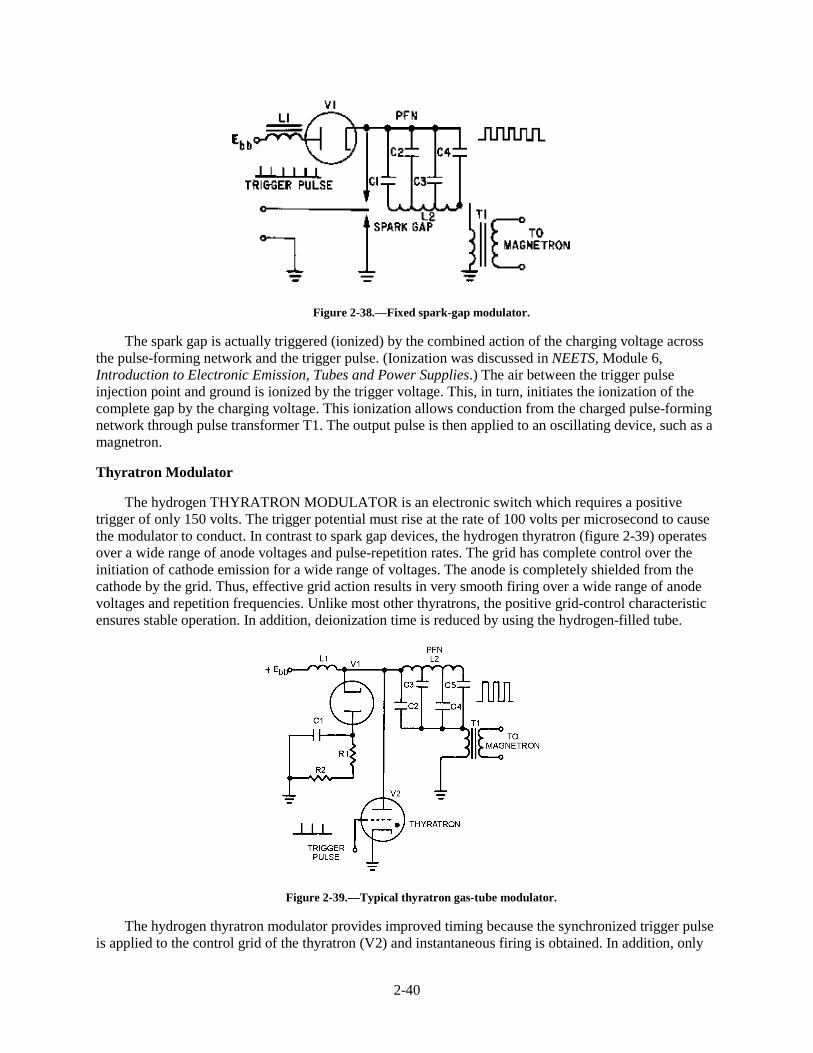
2-40
Figure 2-38.—Fixed spark-gap modulator.
The spark gap is actually triggered (ionized) by the combined action of the charging voltage acrossthe pulse-forming network and the trigger pulse. (Ionization was discussed in NEETS, Module 6,Introduction to Electronic Emission, Tubes and Power Supplies.) The air between the trigger pulseinjection point and ground is ionized by the trigger voltage. This, in turn, initiates the ionization of thecomplete gap by the charging voltage. This ionization allows conduction from the charged pulse-formingnetwork through pulse transformer T1. The output pulse is then applied to an oscillating device, such as amagnetron.
Thyratron Modulator
The hydrogen THYRATRON MODULATOR is an electronic switch which requires a positivetrigger of only 150 volts. The trigger potential must rise at the rate of 100 volts per microsecond to causethe modulator to conduct. In contrast to spark gap devices, the hydrogen thyratron (figure 2-39) operatesover a wide range of anode voltages and pulse-repetition rates. The grid has complete control over theinitiation of cathode emission for a wide range of voltages. The anode is completely shielded from thecathode by the grid. Thus, effective grid action results in very smooth firing over a wide range of anodevoltages and repetition frequencies. Unlike most other thyratrons, the positive grid-control characteristicensures stable operation. In addition, deionization time is reduced by using the hydrogen-filled tube.
Figure 2-39.—Typical thyratron gas-tube modulator.
The hydrogen thyratron modulator provides improved timing because the synchronized trigger pulseis applied to the control grid of the thyratron (V2) and instantaneous firing is obtained. In addition, only
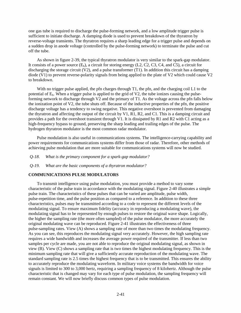
2-41
one gas tube is required to discharge the pulse-forming network, and a low amplitude trigger pulse issufficient to initiate discharge. A damping diode is used to prevent breakdown of the thyratron byreverse-voltage transients. The thyratron requires a sharp leading edge for a trigger pulse and depends ona sudden drop in anode voltage (controlled by the pulse-forming network) to terminate the pulse and cutoff the tube.
As shown in figure 2-39, the typical thyratron modulator is very similar to the spark-gap modulator.It consists of a power source (Eb), a circuit for storing energy (L2, C2, C3, C4, and C5), a circuit fordischarging the storage circuit (V2), and a pulse transformer (T1). In addition this circuit has a dampingdiode (V1) to prevent reverse-polarity signals from being applied to the plate of V2 which could cause V2to breakdown.
With no trigger pulse applied, the pfn charges through T1, the pfn, and the charging coil L1 to thepotential of Eb. When a trigger pulse is applied to the grid of V2, the tube ionizes causing the pulse-forming network to discharge through V2 and the primary of T1. As the voltage across the pfn falls belowthe ionization point of V2, the tube shuts off. Because of the inductive properties of the pfn, the positivedischarge voltage has a tendency to swing negative. This negative overshoot is prevented from damagingthe thyratron and affecting the output of the circuit by V1, R1, R2, and C1. This is a damping circuit andprovides a path for the overshoot transient through V1. It is dissipated by R1 and R2 with C1 acting as ahigh-frequency bypass to ground, preserving the sharp leading and trailing edges of the pulse. Thehydrogen thyratron modulator is the most common radar modulator.
Pulse modulation is also useful in communications systems. The intelligence-carrying capability andpower requirements for communications systems differ from those of radar. Therefore, other methods ofachieving pulse modulation that are more suitable for communications systems will now be studied.
Q-18. What is the primary component for a spark-gap modulator?
Q-19. What are the basic components of a thyratron modulator?
COMMUNICATIONS PULSE MODULATORS
To transmit intelligence using pulse modulation, you must provide a method to vary somecharacteristic of the pulse train in accordance with the modulating signal. Figure 2-40 illustrates a simplepulse train. The characteristics of these pulses that can be varied are amplitude, pulse width,pulse-repetition time, and the pulse position as compared to a reference. In addition to these threecharacteristics, pulses may be transmitted according to a code to represent the different levels of themodulating signal. To ensure maximum fidelity (accuracy in reproducing a modulating wave), themodulating signal has to be represented by enough pulses to restore the original wave shape. Logically,the higher the sampling rate (the more often sampled) of the pulse modulator, the more accurately theoriginal modulating wave can be reproduced. Figure 2-41 illustrates the effectiveness of threepulse-sampling rates. View (A) shows a sampling rate of more than two times the modulating frequency.As you can see, this reproduces the modulating signal very accurately. However, the high sampling raterequires a wide bandwidth and increases the average power required of the transmitter. If less than twosamples per cycle are made, you are not able to reproduce the original modulating signal, as shown inview (B). View (C) shows a sampling rate that is two times the highest modulating frequency. This is theminimum sampling rate that will give a sufficiently accurate reproduction of the modulating wave. Thestandard sampling rate is 2.5 times the highest frequency that is to be transmitted. This ensures the abilityto accurately reproduce the modulating waveform. In military voice systems the bandwidth for voicesignals is limited to 300 to 3,000 hertz, requiring a sampling frequency of 8 kilohertz. Although the pulsecharacteristic that is changed may vary for each type of pulse modulation, the sampling frequency willremain constant. We will now briefly discuss common types of pulse modulation.
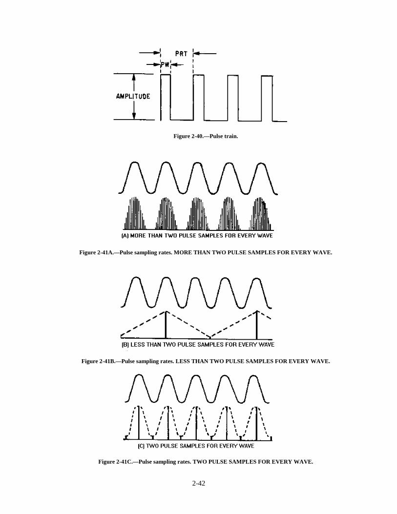
2-42
Figure 2-40.—Pulse train.
Figure 2-41A.—Pulse sampling rates. MORE THAN TWO PULSE SAMPLES FOR EVERY WAVE.
Figure 2-41B.—Pulse sampling rates. LESS THAN TWO PULSE SAMPLES FOR EVERY WAVE.
Figure 2-41C.—Pulse sampling rates. TWO PULSE SAMPLES FOR EVERY WAVE.
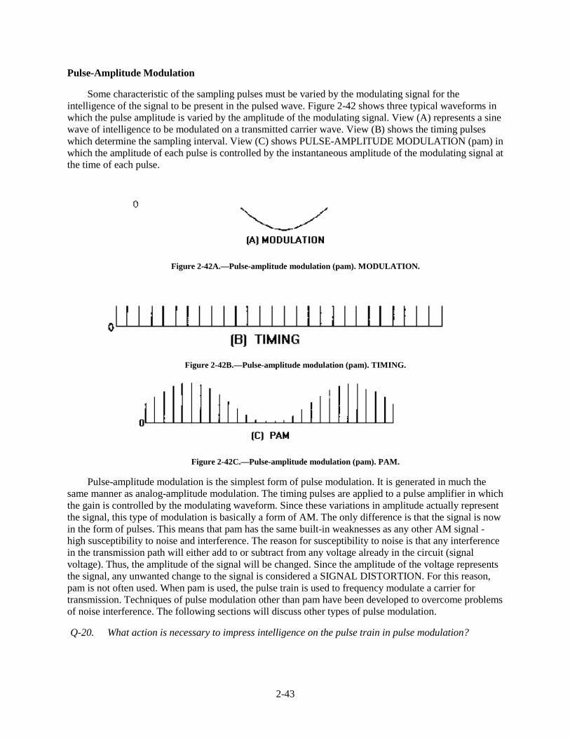
2-43
Pulse-Amplitude Modulation
Some characteristic of the sampling pulses must be varied by the modulating signal for theintelligence of the signal to be present in the pulsed wave. Figure 2-42 shows three typical waveforms inwhich the pulse amplitude is varied by the amplitude of the modulating signal. View (A) represents a sinewave of intelligence to be modulated on a transmitted carrier wave. View (B) shows the timing pulseswhich determine the sampling interval. View (C) shows PULSE-AMPLITUDE MODULATION (pam) inwhich the amplitude of each pulse is controlled by the instantaneous amplitude of the modulating signal atthe time of each pulse.
Figure 2-42A.—Pulse-amplitude modulation (pam). MODULATION.
Figure 2-42B.—Pulse-amplitude modulation (pam). TIMING.
Figure 2-42C.—Pulse-amplitude modulation (pam). PAM.
Pulse-amplitude modulation is the simplest form of pulse modulation. It is generated in much thesame manner as analog-amplitude modulation. The timing pulses are applied to a pulse amplifier in whichthe gain is controlled by the modulating waveform. Since these variations in amplitude actually representthe signal, this type of modulation is basically a form of AM. The only difference is that the signal is nowin the form of pulses. This means that pam has the same built-in weaknesses as any other AM signal -high susceptibility to noise and interference. The reason for susceptibility to noise is that any interferencein the transmission path will either add to or subtract from any voltage already in the circuit (signalvoltage). Thus, the amplitude of the signal will be changed. Since the amplitude of the voltage representsthe signal, any unwanted change to the signal is considered a SIGNAL DISTORTION. For this reason,pam is not often used. When pam is used, the pulse train is used to frequency modulate a carrier fortransmission. Techniques of pulse modulation other than pam have been developed to overcome problemsof noise interference. The following sections will discuss other types of pulse modulation.
Q-20. What action is necessary to impress intelligence on the pulse train in pulse modulation?

2-44
Q-21. To ensure the accuracy of a transmission, what is the minimum number of times a modulatingwave should be sampled in pulse modulation?
Q-22. What, if any, noise susceptibility advantage exists for pulse-amplitude modulation over analog-amplitude modulation?
Pulse-Time Modulation
In pulse-modulated systems, as in an analog system, the intelligence may be impressed on the carrierby varying any of its characteristics. In the preceding paragraphs the method of modulating a pulse trainby varying its amplitude was discussed. Time characteristics of pulses may also be modulated withintelligence information. Two time characteristics may be affected: (1) the time duration of the pulses,referred to as PULSE-DURATION MODULATION (pdm) or PULSE-WIDTH MODULATION (pwm);and (2) the time of occurrence of the pulses, referred to as PULSE-POSITION MODULATION (ppm),and a special type of PULSE-TIME MODULATION (ptm) referred to as PULSE-FREQUENCYMODULATION (pfm). Figure 2-43 shows these types of ptm in views (C), (D), and (E). Views (A) and(B) show the modulating signal and timing, respectively.
Figure 2-43A.—Pulse-time modulation (ptm). MODULATION.
Figure 2-43B.—Pulse-time modulation (ptm). TIMING.
Figure 2-43C.—Pulse-time modulation (ptm). PDM.
Figure 2-43D.—Pulse-time modulation (ptm). PPM.
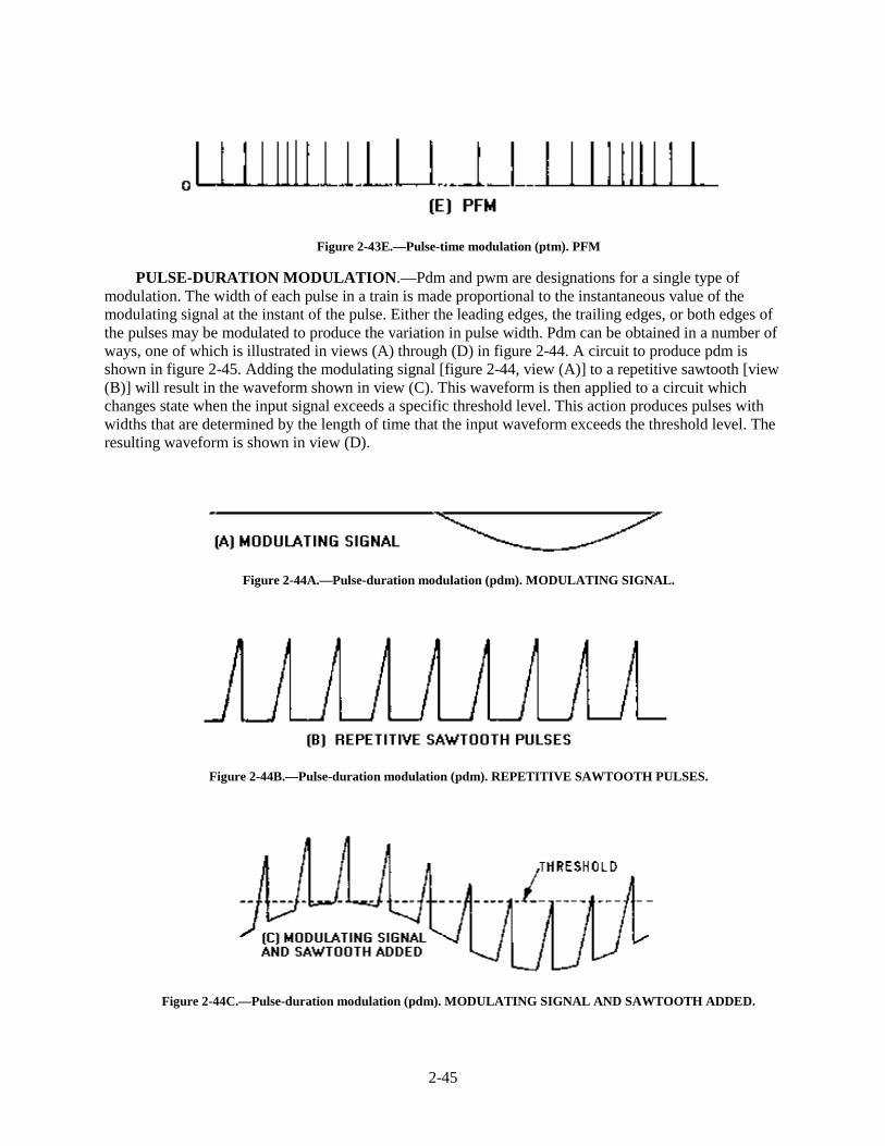
2-45
Figure 2-43E.—Pulse-time modulation (ptm). PFM
PULSE-DURATION MODULATION.—Pdm and pwm are designations for a single type ofmodulation. The width of each pulse in a train is made proportional to the instantaneous value of themodulating signal at the instant of the pulse. Either the leading edges, the trailing edges, or both edges ofthe pulses may be modulated to produce the variation in pulse width. Pdm can be obtained in a number ofways, one of which is illustrated in views (A) through (D) in figure 2-44. A circuit to produce pdm isshown in figure 2-45. Adding the modulating signal [figure 2-44, view (A)] to a repetitive sawtooth [view(B)] will result in the waveform shown in view (C). This waveform is then applied to a circuit whichchanges state when the input signal exceeds a specific threshold level. This action produces pulses withwidths that are determined by the length of time that the input waveform exceeds the threshold level. Theresulting waveform is shown in view (D).
Figure 2-44A.—Pulse-duration modulation (pdm). MODULATING SIGNAL.
Figure 2-44B.—Pulse-duration modulation (pdm). REPETITIVE SAWTOOTH PULSES.
Figure 2-44C.—Pulse-duration modulation (pdm). MODULATING SIGNAL AND SAWTOOTH ADDED.

2-46
Figure 2-44D.—Pulse-duration modulation (pdm). WIDTH MODULATED PULSES FROM CIRCUIT OFFIGURE 2-45.
Figure 2-45.—Circuit for producing pdm.
In the circuit of figure 2-45, a series of sawtooth pulses, occurring at the sampling rate, is applied toa one-shot multivibrator. The multivibrator has the signal voltage Essuperimposed on the bias voltage Ein.Each pulse triggers a cycle of multivibrator operation which terminates after a time interval and varieslinearly with the voltage Es. The pulse of plate voltage produced by the multivibrator will have a leadingedge at T1. The leading edge will vary in position with the signal voltage, while the trailing edge at T2 isfixed by the termination of the sawtooth pulse. The length of the output pulse is thus duration or widthmodulated. If the sawtooth has an instantaneous buildup and a sloping trailing edge, then the leading edge(T1) is fixed and the trailing edge (T2) varies. If the sawtooth generator produces a slope on both leadingand trailing edges, both T1 and T2 are variable in position, but the result is still pdm. Pdm is often usedbecause it is of a constant amplitude and is, therefore, less susceptible to noise. When compared withppm, pdm has the disadvantage of a varying pulse, width and, therefore, of varying power content. Thismeans that the transmitter must be powerful enough to handle the maximum-width pulses, although theaverage power transmitted is much less than peak power. On the other hand, pdm will still work if thesynchronization between the transmitter and receiver fails; in ppm it will not, as will be seen in the nextsection.
PULSE-POSITION MODULATION.—The amplitude and width of the pulse is kept constant inthe system. The position of each pulse, in relation to the position of a recurrent reference pulse, is variedby each instantaneous sampled value of the modulating wave. Ppm has the advantage of requiringconstant transmitter power since the pulses are of constant amplitude and duration. It is widely used buthas the disadvantage of depending on transmitter-receiver synchronization.
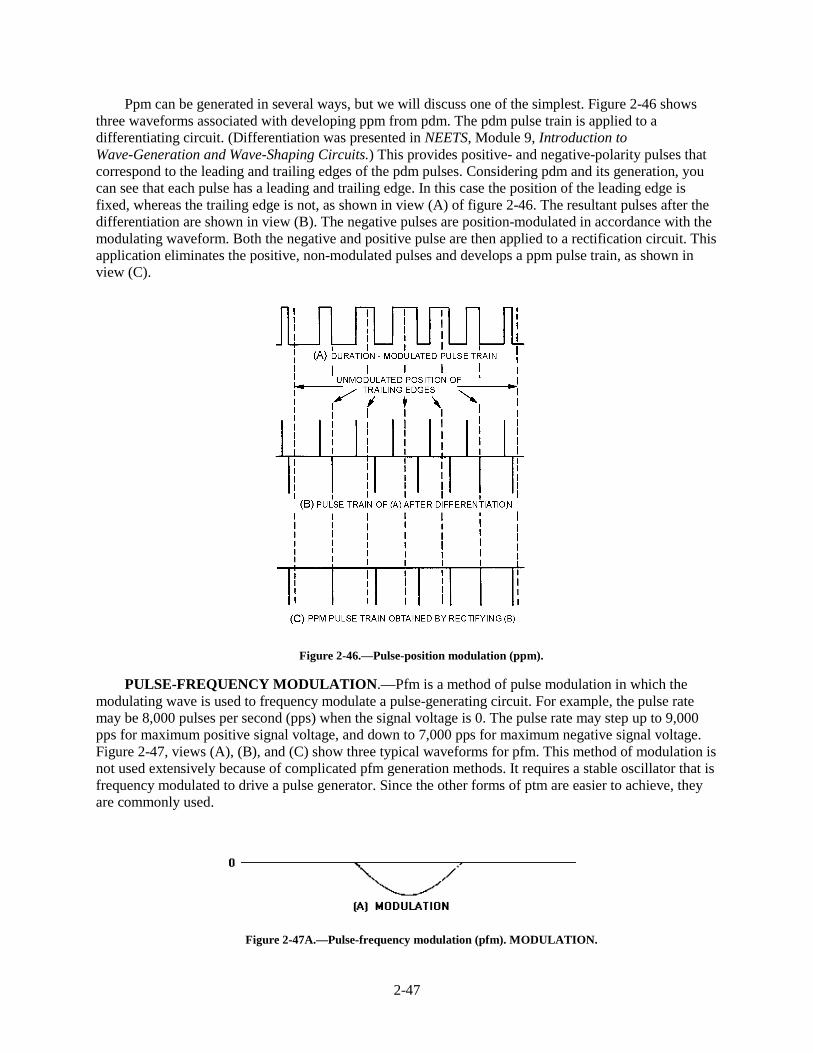
2-47
Ppm can be generated in several ways, but we will discuss one of the simplest. Figure 2-46 showsthree waveforms associated with developing ppm from pdm. The pdm pulse train is applied to adifferentiating circuit. (Differentiation was presented in NEETS, Module 9, Introduction toWave-Generation and Wave-Shaping Circuits.) This provides positive- and negative-polarity pulses thatcorrespond to the leading and trailing edges of the pdm pulses. Considering pdm and its generation, youcan see that each pulse has a leading and trailing edge. In this case the position of the leading edge isfixed, whereas the trailing edge is not, as shown in view (A) of figure 2-46. The resultant pulses after thedifferentiation are shown in view (B). The negative pulses are position-modulated in accordance with themodulating waveform. Both the negative and positive pulse are then applied to a rectification circuit. Thisapplication eliminates the positive, non-modulated pulses and develops a ppm pulse train, as shown inview (C).
Figure 2-46.—Pulse-position modulation (ppm).
PULSE-FREQUENCY MODULATION.—Pfm is a method of pulse modulation in which themodulating wave is used to frequency modulate a pulse-generating circuit. For example, the pulse ratemay be 8,000 pulses per second (pps) when the signal voltage is 0. The pulse rate may step up to 9,000pps for maximum positive signal voltage, and down to 7,000 pps for maximum negative signal voltage.Figure 2-47, views (A), (B), and (C) show three typical waveforms for pfm. This method of modulation isnot used extensively because of complicated pfm generation methods. It requires a stable oscillator that isfrequency modulated to drive a pulse generator. Since the other forms of ptm are easier to achieve, theyare commonly used.
Figure 2-47A.—Pulse-frequency modulation (pfm). MODULATION.
2-48
Figure 2-47B.—Pulse-frequency modulation (pfm). TIMING.
Figure 2-47C.—Pulse-frequency modulation (pfm). PFM.
Q-23. What characteristics of a pulse can be changed in pulse-time modulation?
Q-24. Which edges of the pulse can be modulated in pulse-duration modulation?
Q-25. What is the main disadvantage of pulse-position modulation?
Q-26. What is pulse-frequency modulation?
Pulse-Code Modulation
PULSE-CODE MODULATION (pcm) refers to a system in which the standard values of aQUANTIZED WAVE (explained in the following paragraphs) are indicated by a series of coded pulses.When these pulses are decoded, they indicate the standard values of the original quantized wave. Thesecodes may be binary, in which the symbol for each quantized element will consist of pulses and spaces:ternary, where the code for each element consists of any one of three distinct kinds of values (such aspositive pulses, negative pulses, and spaces); or n-ary, in which the code for each element consists of naynumber (n) of distinct values. This discussion will be based on the binary pcm system.
All of the pulse-modulation systems discussed previously provide methods of converting analogwave shapes to digital wave shapes (pulses occurring at discrete intervals, some characteristic of which isvaried as a continuous function of the analog wave). The entire range of amplitude (frequency or phase)values of the analog wave can be arbitrarily divided into a series of standard values. Each pulse of a pulsetrain [figure 2-48, view (B)] takes the standard value nearest its actual value when modulated. Themodulating wave can be faithfully reproduced, as shown in views (C) and (D). The amplitude range hasbeen divided into 5 standard values in view (C). Each pulse is given whatever standard value is nearest itsactual instantaneous value. In view (D), the same amplitude range has been divided into 10 standardlevels. The curve of view (D) is a much closer approximation of the modulating wave, view (A), than isthe 5-level quantized curve in view (C). From this you should see that the greater the number of standardlevels used, the more closely the quantized wave approximates the original. This is also made evident bythe fact that an infinite number of standard levels exactly duplicates the conditions of nonquantization(the original analog waveform).
2-49
Figure 2-48A.—Quantization levels. MODULATION.
Figure 2-48B.—Quantization levels. TIMING.
Figure 2-48C.—Quantization levels. QUANTIZED 5-LEVEL.
Figure 2-48D.—Quantization levels. QUANTIZED 10-LEVEL.
Although the quantization curves of figure 2-48 are based on 5- and 10-level quantization, in actualpractice the levels are usually established at some exponential value of 2, such as 4(22), 8(2 3), 16(24),32(25) . . . N(2n). The reason for selecting levels at exponential values of 2 will become evident in thediscussion of pcm. Quantized fm is similar in every way to quantized AM. That is, the range of frequencydeviation is divided into a finite number of standard values of deviation. Each sampling pulse results in adeviation equal to the standard value nearest the actual deviation at the sampling instant. Similarly, forphase modulation, quantization establishes a set of standard values. Quantization is used mostly inamplitude- and frequency-modulated pulse systems.
Figure 2-49 shows the relationship between decimal numbers, binary numbers, and a pulse-codewaveform that represents the numbers. The table is for a 16-level code; that is, 16 standard values of aquantized wave could be represented by these pulse groups. Only the presence or absence of the pulsesare important. The next step up would be a 32-level code, with each decimal number represented by aseries of five binary digits, rather than the four digits of figure 2-49. Six-digit groups would provide a64-level code, seven digits a 128-level code, and so forth. Figure 2-50 shows the application ofpulse-coded groups to the standard values of a quantized wave.
2-50
Figure 2-49.—Binary numbers and pulse-code equivalents.
Figure 2-50.—Pulse-code modulation of a quantized wave (128 bits).
In figure 2-50 the solid curve represents the unquantized values of a modulating sinusoid. Thedashed curve is reconstructed from the quantized values taken at the sampling interval and shows a veryclose agreement with the original curve. Figure 2-51 is identical to figure 2-50 except that the samplinginterval is four times as great and the reconstructed curve is not faithful to the original. As previouslystated, the sampling rate of a pulsed system must be at least twice the highest modulating frequency to get
2-51
a usable reconstructed modulation curve. At the sampling rate of figure 2-50 and with a 4-element binarycode, 128 bits (presence or absence of pulses) must be transmitted for each cycle of the modulatingfrequency. At the sampling rate of figure 2-51, only 32 bits are required; at the minimum sampling rate,only 8 bits are required.
Figure 2-51.—Pulse-code modulation of a quantized wave (32 bits).
As a matter of convenience, especially to simplify the demodulation of pcm, the pulse trains actuallytransmitted are reversed from those shown in figures 2-49, 2-50, and 2-51; that is, the pulse with thelowest binary value (least significant digit) is transmitted first and the succeeding pulses have increasingbinary values up to the code limit (most significant digit). Pulse coding can be performed in a number ofways using conventional circuitry or by means of special cathode ray coding tubes. One form of codingcircuit is shown in figure 2-52. In this case, the pulse samples are applied to a holding circuit (a capacitorwhich stores pulse amplitude information) and the modulator converts pam to pdm. The pdm pulses arethen used to gate the output of a precision pulse generator that controls the number of pulses applied to abinary counter. The duration of the gate pulse is not necessarily an integral number of the repetitionpulses from the precisely timed clock-pulse generator. Therefore, the clock pulses gated into the binarycounter by the pdm pulse may be a number of pulses plus the leading edge of an additional pulse. This"partial" pulse may have sufficient duration to trigger the counter, or it may not. The counter thusresponds only to integral numbers, effectively quantizing the signal while, at the same time, encoding it.Each bistable stage of the counter stores ZERO or a ONE for each binary digit it represents (binary 1110or decimal 14 is shown in figure 2-52). An electronic commutator samples the 20, 21, 22, and 23 digitpositions in sequence and transmits a mark or space bit (pulse or no pulse) in accordance with the state ofeach counter stage. The holding circuit is always discharged and reset to zero before initiation of thesequence for the next pulse sample.
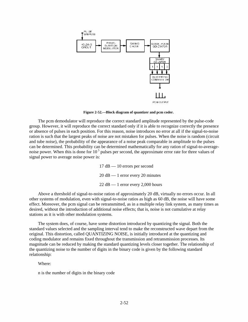
2-52
Figure 2-52.—Block diagram of quantizer and pcm coder.
The pcm demodulator will reproduce the correct standard amplitude represented by the pulse-codegroup. However, it will reproduce the correct standard only if it is able to recognize correctly the presenceor absence of pulses in each position. For this reason, noise introduces no error at all if the signal-to-noiseration is such that the largest peaks of noise are not mistaken for pulses. When the noise is random (circuitand tube noise), the probability of the appearance of a noise peak comparable in amplitude to the pulsescan be determined. This probability can be determined mathematically for any ration of signal-to-average-noise power. When this is done for 10 5 pulses per second, the approximate error rate for three values ofsignal power to average noise power is:
17 dB — 10 errors per second
20 dB — 1 error every 20 minutes
22 dB — 1 error every 2,000 hours
Above a threshold of signal-to-noise ration of approximately 20 dB, virtually no errors occur. In allother systems of modulation, even with signal-to-noise ratios as high as 60 dB, the noise will have someeffect. Moreover, the pcm signal can be retransmitted, as in a multiple relay link system, as many times asdesired, without the introduction of additional noise effects; that is, noise is not cumulative at relaystations as it is with other modulation systems.
The system does, of course, have some distortion introduced by quantizing the signal. Both thestandard values selected and the sampling interval tend to make the reconstructed wave depart from theoriginal. This distortion, called QUANTIZING NOISE, is initially introduced at the quantizing andcoding modulator and remains fixed throughout the transmission and retransmission processes. Itsmagnitude can be reduced by making the standard quantizing levels closer together. The relationship ofthe quantizing noise to the number of digits in the binary code is given by the following standardrelationship:
Where:
n is the number of digits in the binary code
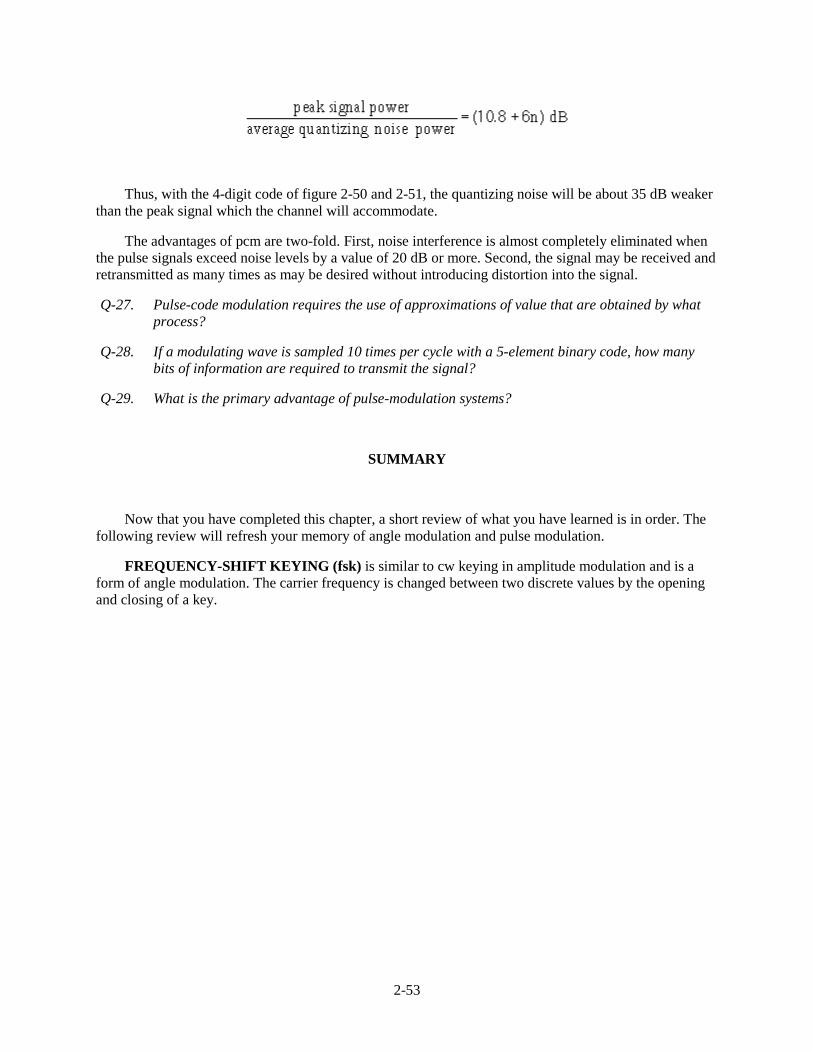
2-53
Thus, with the 4-digit code of figure 2-50 and 2-51, the quantizing noise will be about 35 dB weakerthan the peak signal which the channel will accommodate.
The advantages of pcm are two-fold. First, noise interference is almost completely eliminated whenthe pulse signals exceed noise levels by a value of 20 dB or more. Second, the signal may be received andretransmitted as many times as may be desired without introducing distortion into the signal.
Q-27. Pulse-code modulation requires the use of approximations of value that are obtained by whatprocess?
Q-28. If a modulating wave is sampled 10 times per cycle with a 5-element binary code, how manybits of information are required to transmit the signal?
Q-29. What is the primary advantage of pulse-modulation systems?
SUMMARY
Now that you have completed this chapter, a short review of what you have learned is in order. Thefollowing review will refresh your memory of angle modulation and pulse modulation.
FREQUENCY-SHIFT KEYING (fsk) is similar to cw keying in amplitude modulation and is aform of angle modulation. The carrier frequency is changed between two discrete values by the openingand closing of a key.
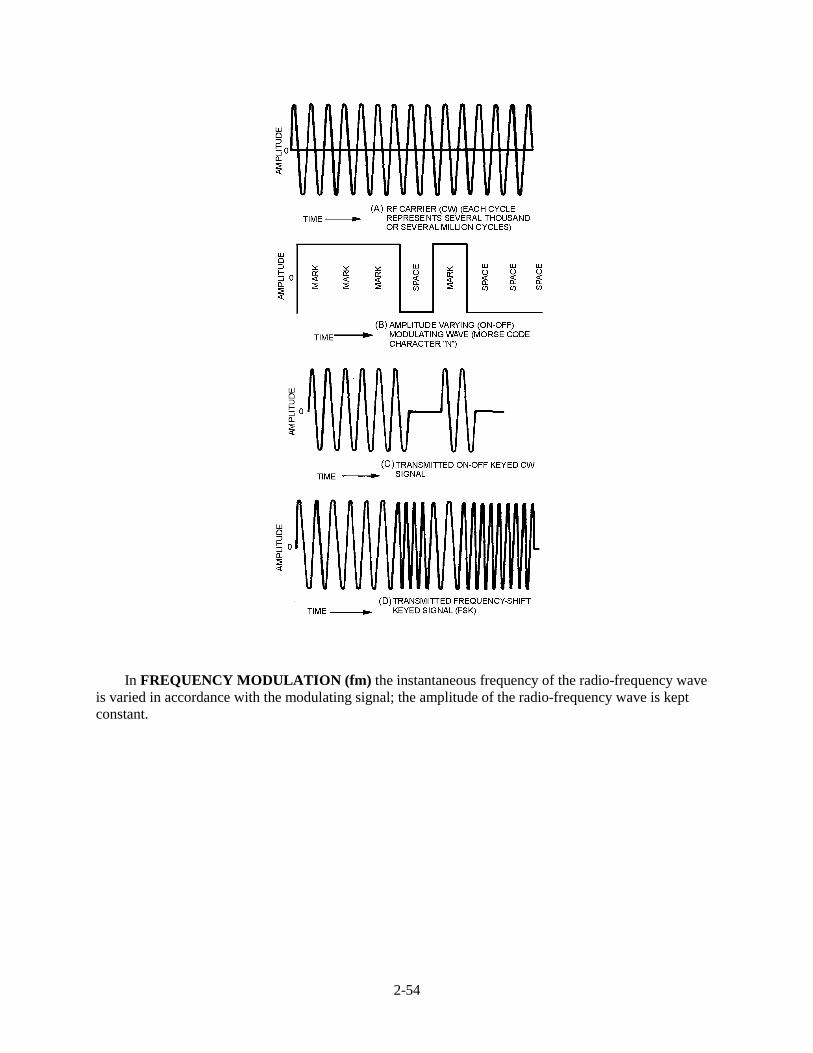
2-54
In FREQUENCY MODULATION (fm) the instantaneous frequency of the radio-frequency waveis varied in accordance with the modulating signal; the amplitude of the radio-frequency wave is keptconstant.

2-55
MODULATION INDEX is the ratio of the maximum frequency difference between the modulatedand the unmodulated carrier, or between the deviation frequency and the modulation frequency.
The number of SIGNIFICANT SIDEBANDS and the modulating frequency will determine thebandwidth of the fm wave. The number of significant sidebands can be determined from the modulationindex.
MODULATIONINDEX
SIGNIFICANTSIDEBANDS
.01 2.4 2.5 4
1.0 62.0 83.0 124.0 145.0 166.0 187.0 228.0 249.0 26
10.0 2811.0 3212.0 3213.0 3614.0 3815.0 38
The REACTANCE-TUBE MODULATOR is frequency modulated by using a reactance tube inshunt with the tank circuit.

2-56
The SEMICONDUCTOR-REACTANCE MODULATOR is used to frequency modulatelow-power semiconductor transmitters.

2-57
The MULTIVIBRATOR MODULATOR uses an astable multivibrator with a modulating voltageinserted in series with the base return of the multivibrator transistors.
The VARACTOR FM MODULATOR uses a VARACTOR. This is a specially designed diode thathas a certain amount of capacitance between the junction that can be controlled by reverse biasing.
In PHASE MODULATION the carrier’s phase is caused to shift at the rate of the modulating audio.The amount of phase shift is controlled by the amplitude of the modulating wave.
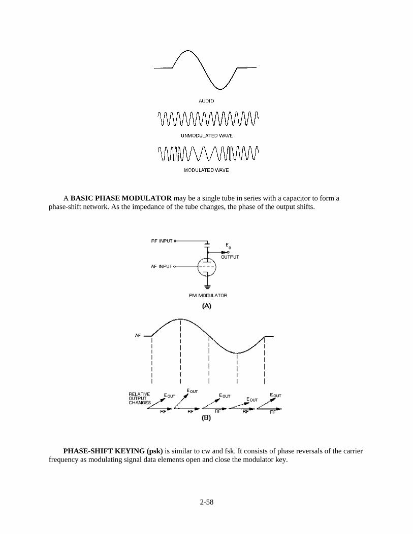
2-58
A BASIC PHASE MODULATOR may be a single tube in series with a capacitor to form aphase-shift network. As the impedance of the tube changes, the phase of the output shifts.
PHASE-SHIFT KEYING (psk) is similar to cw and fsk. It consists of phase reversals of the carrierfrequency as modulating signal data elements open and close the modulator key.
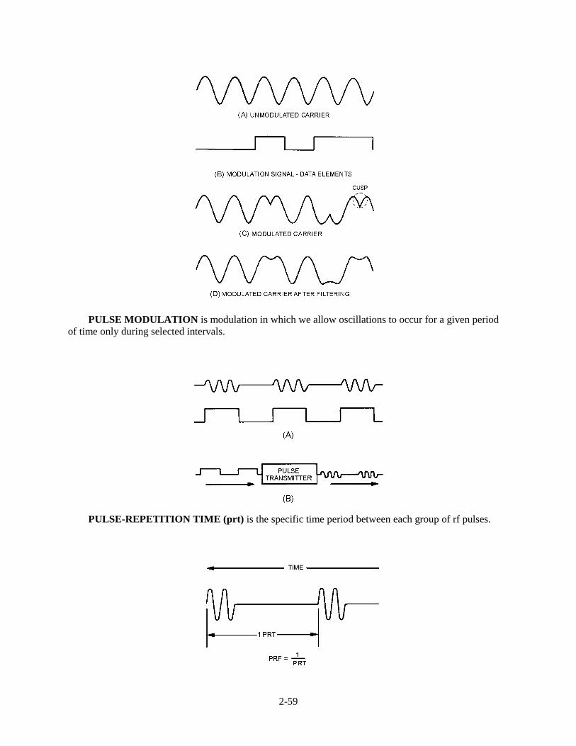
2-59
PULSE MODULATION is modulation in which we allow oscillations to occur for a given periodof time only during selected intervals.
PULSE-REPETITION TIME (prt) is the specific time period between each group of rf pulses.
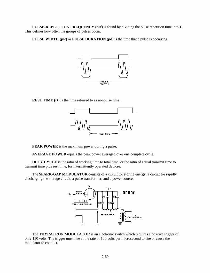
2-60
PULSE-REPETITION FREQUENCY (prf) is found by dividing the pulse repetition time into 1.This defines how often the groups of pulses occur.
PULSE WIDTH (pw) or PULSE DURATION (pd) is the time that a pulse is occurring.
REST TIME (rt) is the time referred to as nonpulse time.
PEAK POWER is the maximum power during a pulse.
AVERAGE POWER equals the peak power averaged over one complete cycle.
DUTY CYCLE is the ratio of working time to total time, or the ratio of actual transmit time totransmit time plus rest time, for intermittently operated devices.
The SPARK-GAP MODULATOR consists of a circuit for storing energy, a circuit for rapidlydischarging the storage circuit, a pulse transformer, and a power source.
The THYRATRON MODULATOR is an electronic switch which requires a positive trigger ofonly 150 volts. The trigger must rise at the rate of 100 volts per microsecond to fire or cause themodulator to conduct.
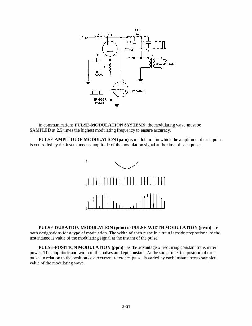
2-61
In communications PULSE-MODULATION SYSTEMS, the modulating wave must beSAMPLED at 2.5 times the highest modulating frequency to ensure accuracy.
PULSE-AMPLITUDE MODULATION (pam) is modulation in which the amplitude of each pulseis controlled by the instantaneous amplitude of the modulation signal at the time of each pulse.
PULSE-DURATION MODULATION (pdm) or PULSE-WIDTH MODULATION (pwm) areboth designations for a type of modulation. The width of each pulse in a train is made proportional to theinstantaneous value of the modulating signal at the instant of the pulse.
PULSE-POSITION MODULATION (ppm) has the advantage of requiring constant transmitterpower. The amplitude and width of the pulses are kept constant. At the same time, the position of eachpulse, in relation to the position of a recurrent reference pulse, is varied by each instantaneous sampledvalue of the modulating wave.
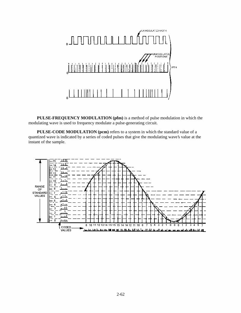
2-62
PULSE-FREQUENCY MODULATION (pfm) is a method of pulse modulation in which themodulating wave is used to frequency modulate a pulse-generating circuit.
PULSE-CODE MODULATION (pcm) refers to a system in which the standard value of aquantized wave is indicated by a series of coded pulses that give the modulating wave’s value at theinstant of the sample.
2-63
ANSWERS TO QUESTIONS Q1. THROUGH Q29.
A-1. Frequency and phase.
A-2. Frequency-shift keying.
A-3. Resistance to noise interference.
A-4. Instantaneous frequency.
A-5. As the ratio of the frequency deviation to the maximum frequency deviation allowable.
A-6. The number of significant sidebands and the modulating frequency.
A-7. By changing the reactance of an oscillator circuit in consonance with the modulating voltage.
A-8. Collector-to-emitter capacitance.
A-9. An LCR filter.
A-10. Capacitance.
A-11. Phase.
A-12. A phase-shift network such as a variable resistor and capacitor in series.
A-13. Cw and frequency-shift keying.
A-14. Pulse modulation.
A-15. Pulse-repetition time.
A-16. Rest time.
A-17. Peak power during a pulse averaged over pulse time plus rest time.
A-18. Either a fixed spark gap that uses a trigger pulse to ionize the air between the contacts, or arotary gap that is similar to a mechanical switch.
A-19. Power source, a circuit for storing energy, a circuit for discharging the storage circuit, and apulse transformer.
A-20. Some characteristic of the pulses has to be varied.
A-21. 2.5 times the highest modulating frequency.
A-22. Both are susceptible to noise and interference.
A-23. The time duration of the pulses or the time of occurrence of the pulses.
A-24. Either, or both at the same time.
A-25. It requires synchronization between the transmitter and receiver.
A-26. A method of pulse modulation in which a modulating wave is used to frequency modulate apulse-generating circuit.

2-64
A-27. Quantization.
A-28. 50.
A-29. Low susceptibility to noise.
3-1
CHAPTER 3
DEMODULATION
LEARNING OBJECTIVES
Upon completion of this chapter you will be able to:
1. Describe cw detector circuit operations for the heterodyne and regenerative detectors.
2. Discuss the requirements for recovery of intelligence from an AM signal and describe the theoryof operation of the following AM demodulators: series-diode, shunt-diode, common-emitter, andcommon-base.
3. Describe fm demodulation circuit operation for the phase-shift and gated-beam discriminatorsand the ratio-detector demodulator.
4. Describe phase demodulation circuit operation for the peak, low-pass filter, and conversiondetectors.
INTRODUCTION
In chapters 1 and 2 you studied how to apply intelligence (modulation) to an rf-carrier wave. Carriermodulation allows the transmission of modulating frequencies without the use of transmission wire as amedium. However, for the communication process to be completed or to be useful, the intelligence mustbe recovered in its original form at the receiving site. The process of re-creating original modulatingfrequencies (intelligence) from the rf carrier is referred to as DEMODULATION or DETECTION. Eachtype of modulation is different and requires different techniques to recover (demodulate) the intelligence.In this chapter we will discuss ways of demodulating AM, cw, fm, phase, and pulse modulation.
The circuit in which restoration is achieved is called the DETECTOR or DEMODULATOR (both ofthese terms are used in NEETS). The term demodulator is used because the demodulation process isconsidered to be the opposite of modulation. The output of an ideal detector must be an exactreproduction of the modulation existing on the rf wave. Failure to accurately recover this intelligence willresult in distortion and degradation of the demodulated signal and intelligence will be lost. The distortionmay be in amplitude, frequency, or phase, depending on the nature of the demodulator. A nonlineardevice is required for demodulation. This nonlinear device is required to recover the modulatingfrequencies from the rf envelope. Solid-state detector circuits may be either a pn junction diode or theinput junction of a transistor. In electron-tube circuits, either a diode or the grid or plate circuits of atriode electron tube may be used as the nonlinear device.
Q-1. What is demodulation?
Q-2. What is a demodulator?
3-2
CONTINUOUS-WAVE DEMODULATION
Continuous-wave (cw) modulation consists of on-off keying of a carrier wave. To recover on-offkeyed information, we need a method of detecting the presence or absence of rf oscillations. The CWDEMODULATOR detects the presence of rf oscillations and converts them into a recognizable form.Figure 3-1 illustrates the received cw in view (A), the rectified cw from a diode detector in view (B), andthe dc output from a filter that can be used to control a relay or light indicator in view (C).
Figure 3-1A.—Cw demodulation. RECEIVED CW.
Figure 3-1B.—Cw demodulation. RECTIFIED CW FROM DETECTOR.
Figure 3-1C.—Cw demodulation. OUTPUT FROM FILTER.
Figure 3-2 is a, simplified circuit that could be used as a cw demodulator. The antenna receives the rfoscillations from the transmitter. The tank circuit, L and C1, acts as a frequency-selective network that istuned to the desired rf carrier frequency. The diode rectifies the oscillations and C2 provides filtering toprovide a constant dc output to control the headset. This demodulator circuit is the equivalent of a wiretelegraphy circuit but it has certain disadvantages. For example, if two transmitters are very close infrequency, distinguishing which transmitting station you are receiving is often impossible without amethod of fine tuning the desired frequency. Also, if the stations are within the frequency bandpass of theinput tank circuit, the tank output will contain a mixture of both signals. Therefore, a method, such asHETERODYNE DETECTION, must be used which provides more than just the information on thepresence or absence of a signal.
3-3
Figure 3-2.—Cw demodulator.
HETERODYNE DETECTION
The use of an af voltage in the detector aids the operator in distinguishing between various signals.Since the carrier is unmodulated, the af voltage can be developed by using the heterodyne procedurediscussed in chapter 1. The procedure is to mix the incoming cw signal with locally generatedoscillations. This provides a convenient difference frequency in the af range, such as 1,000 hertz. The afdifference frequency then is rectified and smoothed by a detector. The af voltage is reproduced by atelephone headset or a loudspeaker.
Consider the heterodyne reception of the code letter A, as shown in figure 3-3, view (A). The codeconsists of a short burst of cw energy (dot) followed by a longer burst (dash). Assume that the frequencyof the received cw signal is 500 kilohertz. The locally generated oscillations are adjusted to a frequencywhich is higher or lower than the incoming rf signal (501 kilohertz in this case), as shown in view (B).The voltage resulting from the heterodyning action between the cw signal [view (A)] and the localoscillator signal [view (B)] is shown in view (C) as the mixed-frequency signal. ENVELOPE(intelligence) amplitude varies at the BEAT (difference) frequency of 1,000 hertz (501,000 − 500,000).The negative half cycles of the mixed frequency are rectified, as shown in view (D). The peaks of thepositive half cycles follow the 1,000-hertz beat frequency.
Figure 3-3A.—Heterodyne detection. RECEIVED CW SIGNAL.
Figure 3-3B.—Heterodyne detection. LOCAL OSCILLATOR SIGNAL.
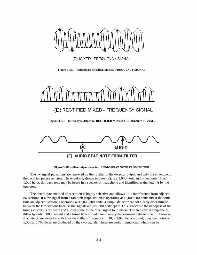
3-4
Figure 3-3C.—Heterodyne detection. MIXED-FREQUENCY SIGNAL.
Figure 3-3D.—Heterodyne detection. RECTIFIED MIXED-FREQUENCY SIGNAL.
Figure 3-3E.—Heterodyne detection. AUDIO-BEAT NOTE FROM FILTER.
The cw signal pulsations are removed by the rf filter in the detector output and only the envelope ofthe rectified pulses remains. The envelope, shown in view (E), is a 1,000-hertz audio-beat note. This1,000 hertz, dot-dash tone may be heard in a speaker or headphone and identified as the letter A by theoperator.
The heterodyne method of reception is highly selective and allows little interference from adjacentcw stations. If a cw signal from a radiotelegraph station is operating at 10,000,000 hertz and at the sametime an adjacent station is operating at 10,000,300 hertz, a simple detector cannot clearly discriminatebetween the two stations because the signals are just 300 hertz apart. This is because the bandpass of thetuning circuits is too wide and allows some of the other signal to interfere. The two carrier frequenciesdiffer by only 0.003 percent and a tuned tank circuit cannot easily discriminate between them. However,if a heterodyne detector with a local-oscillator frequency of 10,001,000 hertz is used, then beat notes of1,000 and 700 hertz are produced by the two signals. These are audio frequencies, which can be
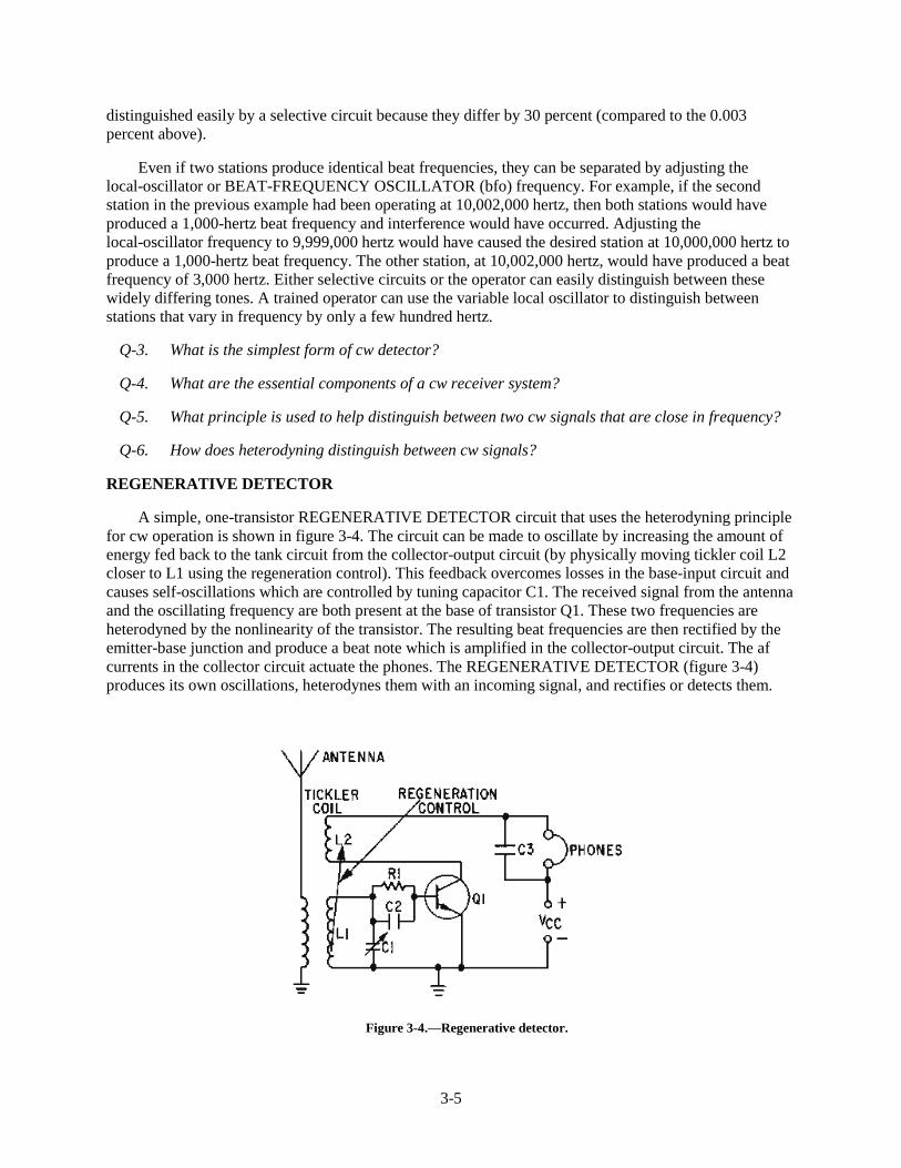
3-5
distinguished easily by a selective circuit because they differ by 30 percent (compared to the 0.003percent above).
Even if two stations produce identical beat frequencies, they can be separated by adjusting thelocal-oscillator or BEAT-FREQUENCY OSCILLATOR (bfo) frequency. For example, if the secondstation in the previous example had been operating at 10,002,000 hertz, then both stations would haveproduced a 1,000-hertz beat frequency and interference would have occurred. Adjusting thelocal-oscillator frequency to 9,999,000 hertz would have caused the desired station at 10,000,000 hertz toproduce a 1,000-hertz beat frequency. The other station, at 10,002,000 hertz, would have produced a beatfrequency of 3,000 hertz. Either selective circuits or the operator can easily distinguish between thesewidely differing tones. A trained operator can use the variable local oscillator to distinguish betweenstations that vary in frequency by only a few hundred hertz.
Q-3. What is the simplest form of cw detector?
Q-4. What are the essential components of a cw receiver system?
Q-5. What principle is used to help distinguish between two cw signals that are close in frequency?
Q-6. How does heterodyning distinguish between cw signals?
REGENERATIVE DETECTOR
A simple, one-transistor REGENERATIVE DETECTOR circuit that uses the heterodyning principlefor cw operation is shown in figure 3-4. The circuit can be made to oscillate by increasing the amount ofenergy fed back to the tank circuit from the collector-output circuit (by physically moving tickler coil L2closer to L1 using the regeneration control). This feedback overcomes losses in the base-input circuit andcauses self-oscillations which are controlled by tuning capacitor C1. The received signal from the antennaand the oscillating frequency are both present at the base of transistor Q1. These two frequencies areheterodyned by the nonlinearity of the transistor. The resulting beat frequencies are then rectified by theemitter-base junction and produce a beat note which is amplified in the collector-output circuit. The afcurrents in the collector circuit actuate the phones. The REGENERATIVE DETECTOR (figure 3-4)produces its own oscillations, heterodynes them with an incoming signal, and rectifies or detects them.
Figure 3-4.—Regenerative detector.
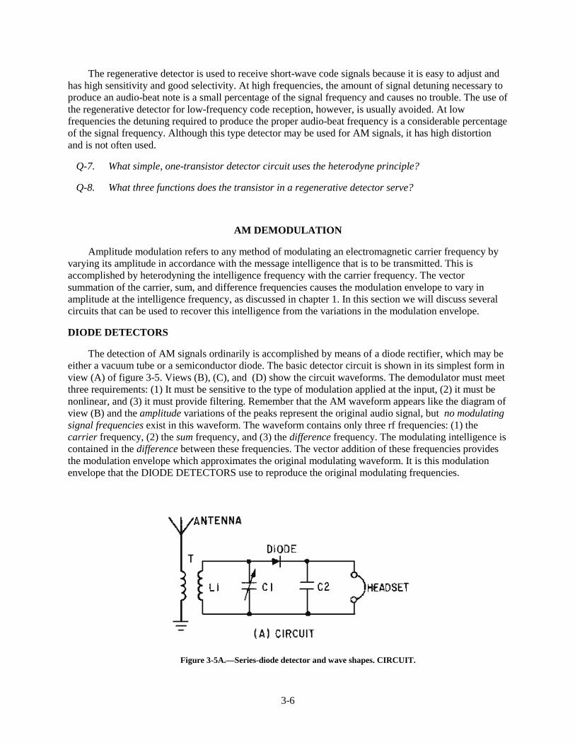
3-6
The regenerative detector is used to receive short-wave code signals because it is easy to adjust andhas high sensitivity and good selectivity. At high frequencies, the amount of signal detuning necessary toproduce an audio-beat note is a small percentage of the signal frequency and causes no trouble. The use ofthe regenerative detector for low-frequency code reception, however, is usually avoided. At lowfrequencies the detuning required to produce the proper audio-beat frequency is a considerable percentageof the signal frequency. Although this type detector may be used for AM signals, it has high distortionand is not often used.
Q-7. What simple, one-transistor detector circuit uses the heterodyne principle?
Q-8. What three functions does the transistor in a regenerative detector serve?
AM DEMODULATION
Amplitude modulation refers to any method of modulating an electromagnetic carrier frequency byvarying its amplitude in accordance with the message intelligence that is to be transmitted. This isaccomplished by heterodyning the intelligence frequency with the carrier frequency. The vectorsummation of the carrier, sum, and difference frequencies causes the modulation envelope to vary inamplitude at the intelligence frequency, as discussed in chapter 1. In this section we will discuss severalcircuits that can be used to recover this intelligence from the variations in the modulation envelope.
DIODE DETECTORS
The detection of AM signals ordinarily is accomplished by means of a diode rectifier, which may beeither a vacuum tube or a semiconductor diode. The basic detector circuit is shown in its simplest form inview (A) of figure 3-5. Views (B), (C), and (D) show the circuit waveforms. The demodulator must meetthree requirements: (1) It must be sensitive to the type of modulation applied at the input, (2) it must benonlinear, and (3) it must provide filtering. Remember that the AM waveform appears like the diagram ofview (B) and the amplitude variations of the peaks represent the original audio signal, but no modulatingsignal frequencies exist in this waveform. The waveform contains only three rf frequencies: (1) thecarrier frequency, (2) the sum frequency, and (3) the difference frequency. The modulating intelligence iscontained in the difference between these frequencies. The vector addition of these frequencies providesthe modulation envelope which approximates the original modulating waveform. It is this modulationenvelope that the DIODE DETECTORS use to reproduce the original modulating frequencies.
Figure 3-5A.—Series-diode detector and wave shapes. CIRCUIT.
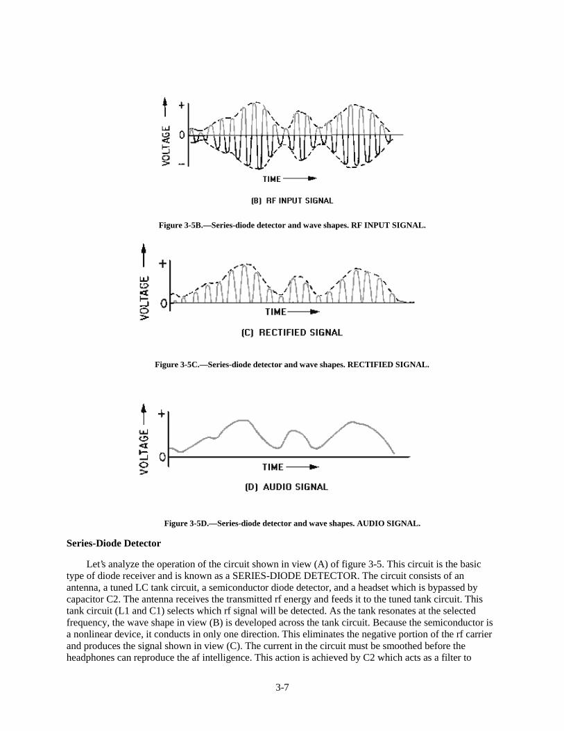
3-7
Figure 3-5B.—Series-diode detector and wave shapes. RF INPUT SIGNAL.
Figure 3-5C.—Series-diode detector and wave shapes. RECTIFIED SIGNAL.
Figure 3-5D.—Series-diode detector and wave shapes. AUDIO SIGNAL.
Series-Diode Detector
Let’s analyze the operation of the circuit shown in view (A) of figure 3-5. This circuit is the basictype of diode receiver and is known as a SERIES-DIODE DETECTOR. The circuit consists of anantenna, a tuned LC tank circuit, a semiconductor diode detector, and a headset which is bypassed bycapacitor C2. The antenna receives the transmitted rf energy and feeds it to the tuned tank circuit. Thistank circuit (L1 and C1) selects which rf signal will be detected. As the tank resonates at the selectedfrequency, the wave shape in view (B) is developed across the tank circuit. Because the semiconductor isa nonlinear device, it conducts in only one direction. This eliminates the negative portion of the rf carrierand produces the signal shown in view (C). The current in the circuit must be smoothed before theheadphones can reproduce the af intelligence. This action is achieved by C2 which acts as a filter to
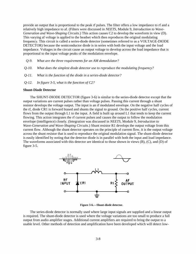
3-8
provide an output that is proportional to the peak rf pulses. The filter offers a low impedance to rf and arelatively high impedance to af. (Filters were discussed in NEETS, Module 9, Introduction to Wave-Generation and Wave-Shaping Circuits.) This action causes C2 to develop the waveform in view (D).This varying af voltage is applied to the headset which then reproduces the original modulatingfrequency. This circuit is called a series-diode detector (sometimes referred to as a VOLTAGE-DIODEDETECTOR) because the semiconductor diode is in series with both the input voltage and the loadimpedance. Voltages in the circuit cause an output voltage to develop across the load impedance that isproportional to the input voltage peaks of the modulation envelope.
Q-9. What are the three requirements for an AM demodulator?
Q-10. What does the simplest diode detector use to reproduce the modulating frequency?
Q-11. What is the function of the diode in a series-diode detector?
Q-12. In figure 3-5, what is the function of C2?
Shunt-Diode Detector
The SHUNT-DIODE DETECTOR (figure 3-6) is similar to the series-diode detector except that theoutput variations are current pulses rather than voltage pulses. Passing this current through a shuntresistor develops the voltage output. The input is an rf modulated envelope. On the negative half cycles ofthe rf, diode CR1 is forward biased and shunts the signal to ground. On the positive half cycles, currentflows from the output through L1 to the input. A field is built up around L1 that tends to keep the currentflowing. This action integrates the rf current pulses and causes the output to follow the modulationenvelope (intelligence) closely. (Integration was discussed in NEETS, Module 9, Introduction toWave-Generation and Wave-Shaping Circuits.) Shunt resistor R1 develops the output voltage from thiscurrent flow. Although the shunt detector operates on the principle of current flow, it is the output voltageacross the shunt resistor that is used to reproduce the original modulation signal. The shunt-diode detectoris easily identified by noting that the detector diode is in parallel with both the input and load impedance.The waveforms associated with this detector are identical to those shown in views (B), (C), and (D) offigure 3-5.
Figure 3-6.—Shunt-diode detector.
The series-diode detector is normally used where large input signals are supplied and a linear outputis required. The shunt-diode detector is used where the voltage variations are too small to produce a fulloutput from audio amplifier stages. Additional current amplifiers are required to bring the output to ausable level. Other methods of detection and amplification have been developed which will detect low-

3-9
level signals. The next sections will discuss two of these circuits, the common-emitter and common-basedetectors.
Q-13. How does the current-diode detector differ from the voltage-diode detector?
Q-14. Under what circuit conditions would the shunt detector be used?
COMMON-EMITTER DETECTOR
The COMMON-EMITTER DETECTOR is often used in receivers to supply an amplified detectedoutput. The schematic for a typical transistor common-emitter detector is shown in figure 3-7. Inputtransformer T1 has a tuned primary that acts as a frequency-selective device. L2 inductively couples theinput modulation envelope to the base of transistor Q1. Resistors R1 and R2 are fixed-bias voltagedividers that set the bias levels for Q1. Resistor R1 is bypassed by C2 to eliminate rf. This RCcombination also acts as the load for the diode detector (emitter-base junction of Q1). The detected audiois in series with the biasing voltage and controls collector current. The output is developed across R4which is also bypassed to remove rf by C4. R3 is a temperature stabilization resistor and C3 bypasses itfor both rf and af.
Figure 3-7.—Common-emitter detector.
Q1 is biased for slight conduction with no input signal applied. When an input signal appears on thebase of Q1, it is rectified by the emitter-base junction (operating as a diode) and is developed across R1 asa dc bias voltage with a varying af component. This voltage controls bias and collector current for Q1.The output is developed by collector current flow through R4. Any rf ripple in the output is bypassedacross the collector load resistor by capacitor C4. The af variations are not bypassed. After the modulationenvelope is detected in the base circuit, it is amplified in the output circuit to provide suitable af output.The output of this circuit is higher than is possible with a simple detector. Because of the amplification inthis circuit, weaker signals can be detected than with a simple detector. A higher, more usable output isthus developed.
Q-15. Which junction of the transistor in the common-emitter detector detects the modulationenvelope?
Q-16. Which component in figure 3-7 develops the af signal at the input?
Q-17. How is the output signal developed in the common-emitter detector?

3-10
COMMON-BASE DETECTOR
Another amplifying detector that is used in portable receivers is the COMMON-BASE DETECTOR.In this circuit detection occurs in the emitter-base junction and amplification occurs at the output of thecollector junction. The output developed is the equivalent of a diode detector which is followed by a stageof audio amplification, but with more distortion. Figure 3-8 is a schematic of a typical common-basedetector. Transformer T1 is tuned by capacitor C3 to the frequency of the incoming modulated envelope.Resistor R1 and capacitor C1 form a self-biasing network which sets the dc operating point of the emitterjunction. The af output is taken from the collector circuit through audio transformer T2. The primary ofT2 forms the detector output load and is bypassed for rf by capacitor C2.
Figure 3-8.—Common-base detector.
The input signal is coupled through T1. When capacitor C3 is tuned to the proper frequency, thesignal is passed to the emitter of Q1. When no input signal is present, bias is determined by resistor R1.When the input signal becomes positive, current flows through the emitter-base junction causing it to beforward biased. C1 and R1 establish the dc operating point by acting as a filter network. This actionprovides a varying dc voltage that follows the peaks of the rf modulated envelope. This action is identicalto the diode detector with the emitter-base junction doing the detecting. The varying dc voltage on theemitter changes the bias on Q1 and causes collector current to vary in accordance with the detectedvoltage. Transformer T2 couples these af current changes to the output. Thus, Q1 detects the AM waveand then provides amplification for the detected waveform.
The four AM detectors just discussed are not the only types that you will encounter. However, theyare representative of most AM detectors and the same characteristics will be found in all AM detectors.Now let’s study some ways of demodulating frequency-modulated (fm) signals.
Q-18. Which junction acts as the detector in a common-base detector?
Q-19. To what circuit arrangement is a common-base detector equivalent?
Q-20. In figure 3-8, which components act as the filter network in the diode detector?
FM DEMODULATION
In fm demodulators, the intelligence to be recovered is not in amplitude variations; it is in thevariation of the instantaneous frequency of the carrier, either above or below the center frequency. The

3-11
detecting device must be constructed so that its output amplitude will vary linearly according to theinstantaneous frequency of the incoming signal.
Several types of fm detectors have been developed and are in use, but in this section you will studythree of the most common: (1) the phase-shift detector, (2) the ratio detector, and (3) the gated-beamdetector.
SLOPE DETECTION
To be able to understand the principles of operation for fm detectors, you need to first study thesimplest form of frequency-modulation detector, the SLOPE DETECTOR. The slope detector isessentially a tank circuit which is tuned to a frequency either slightly above or below the fm carrierfrequency. View (A) of figure 3-9 is a plot of voltage versus frequency for a tank circuit. The resonantfrequency of the tank is the frequency at point 4. Components are selected so that the resonant frequencyis higher than the frequency of the fm carrier signal at point 2. The entire frequency deviation for the fmsignal falls on the lower slope of the bandpass curve between points 1 and 3. As the fm signal is appliedto the tank circuit in view (B), the output amplitude of the signal varies as its frequency swings closer to,or further from, the resonant frequency of the tank. Frequency variations will still be present in thiswaveform, but it will also develop amplitude variations, as shown in view (B). This is because of theresponse of the tank circuit as it varies with the input frequency. This signal is then applied to the diodedetector in view (C) and the detected waveform is the output. This circuit has the major disadvantage thatany amplitude variations in the rf waveform will pass through the tank circuit and be detected. Thisdisadvantage can be eliminated by placing a limiter circuit before the tank input. (Limiter circuits werediscussed in NEETS, Module 9, Introduction to Wave-Generation and Wave-Shaping Circuits.) Thiscircuit is basically the same as an AM detector with the tank tuned to a higher or lower frequency than thereceived carrier.
Figure 3-9A.—Slope detector. VOLTAGE VERSUS FREQUENCY PLOT.
Figure 3-9B.—Slope detector. TANK CIRCUIT.
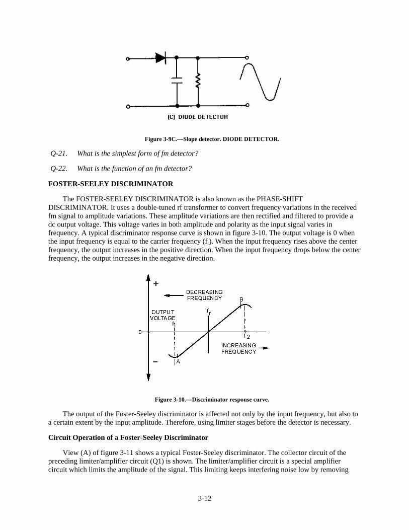
3-12
Figure 3-9C.—Slope detector. DIODE DETECTOR.
Q-21. What is the simplest form of fm detector?
Q-22. What is the function of an fm detector?
FOSTER-SEELEY DISCRIMINATOR
The FOSTER-SEELEY DISCRIMINATOR is also known as the PHASE-SHIFTDISCRIMINATOR. It uses a double-tuned rf transformer to convert frequency variations in the receivedfm signal to amplitude variations. These amplitude variations are then rectified and filtered to provide adc output voltage. This voltage varies in both amplitude and polarity as the input signal varies infrequency. A typical discriminator response curve is shown in figure 3-10. The output voltage is 0 whenthe input frequency is equal to the carrier frequency (fr). When the input frequency rises above the centerfrequency, the output increases in the positive direction. When the input frequency drops below the centerfrequency, the output increases in the negative direction.
Figure 3-10.—Discriminator response curve.
The output of the Foster-Seeley discriminator is affected not only by the input frequency, but also toa certain extent by the input amplitude. Therefore, using limiter stages before the detector is necessary.
Circuit Operation of a Foster-Seeley Discriminator
View (A) of figure 3-11 shows a typical Foster-Seeley discriminator. The collector circuit of thepreceding limiter/amplifier circuit (Q1) is shown. The limiter/amplifier circuit is a special amplifiercircuit which limits the amplitude of the signal. This limiting keeps interfering noise low by removing
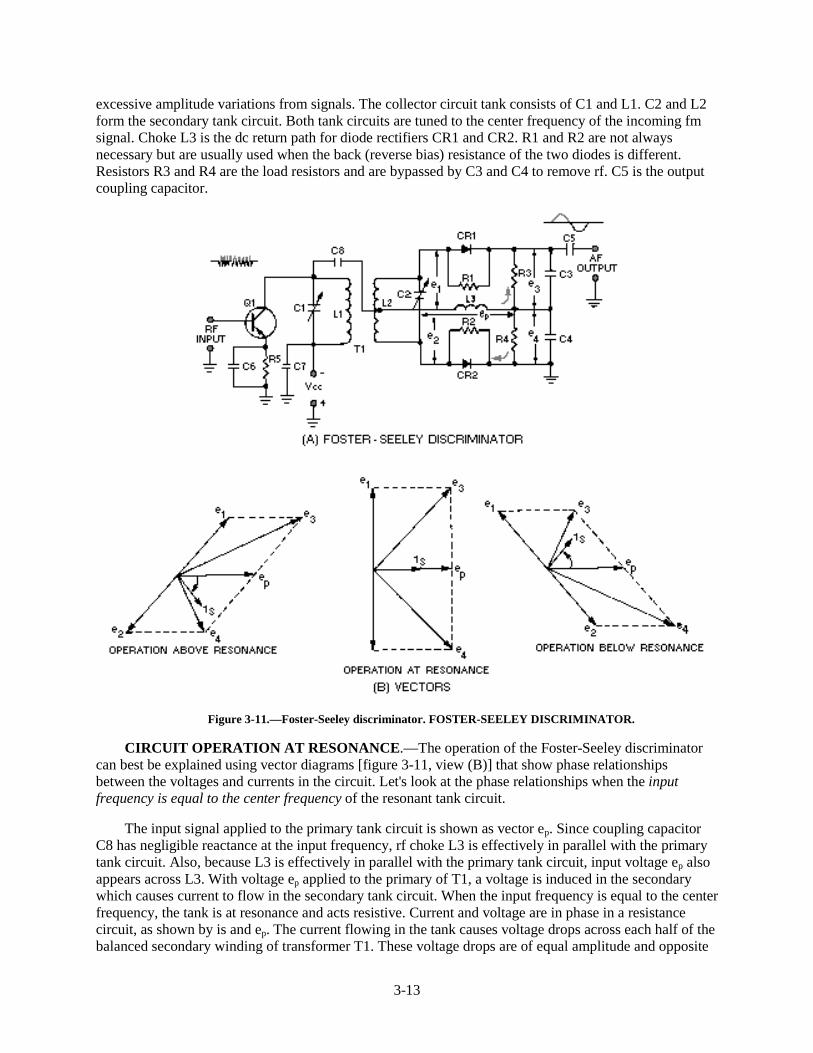
3-13
excessive amplitude variations from signals. The collector circuit tank consists of C1 and L1. C2 and L2form the secondary tank circuit. Both tank circuits are tuned to the center frequency of the incoming fmsignal. Choke L3 is the dc return path for diode rectifiers CR1 and CR2. R1 and R2 are not alwaysnecessary but are usually used when the back (reverse bias) resistance of the two diodes is different.Resistors R3 and R4 are the load resistors and are bypassed by C3 and C4 to remove rf. C5 is the outputcoupling capacitor.
Figure 3-11.—Foster-Seeley discriminator. FOSTER-SEELEY DISCRIMINATOR.
CIRCUIT OPERATION AT RESONANCE.—The operation of the Foster-Seeley discriminatorcan best be explained using vector diagrams [figure 3-11, view (B)] that show phase relationshipsbetween the voltages and currents in the circuit. Let's look at the phase relationships when the inputfrequency is equal to the center frequency of the resonant tank circuit.
The input signal applied to the primary tank circuit is shown as vector ep. Since coupling capacitorC8 has negligible reactance at the input frequency, rf choke L3 is effectively in parallel with the primarytank circuit. Also, because L3 is effectively in parallel with the primary tank circuit, input voltage ep alsoappears across L3. With voltage ep applied to the primary of T1, a voltage is induced in the secondarywhich causes current to flow in the secondary tank circuit. When the input frequency is equal to the centerfrequency, the tank is at resonance and acts resistive. Current and voltage are in phase in a resistancecircuit, as shown by is and ep. The current flowing in the tank causes voltage drops across each half of thebalanced secondary winding of transformer T1. These voltage drops are of equal amplitude and opposite

3-14
polarity with respect to the center tap of the winding. Because the winding is inductive, the voltage acrossit is 90 degrees out of phase with the current through it. Because of the center-tap arrangement, thevoltages at each end of the secondary winding of T1 are 180 degrees out of phase and are shown as e1 ande2 on the vector diagram.
The voltage applied to the anode of CR1 is the vector sum of voltages ep and e1, shown as e 3 on thediagram. Likewise, the voltage applied to the anode of CR2 is the vector sum of voltages ep and e 2,shown as e4 on the diagram. At resonance e3 and e4 are equal, as shown by vectors of the same length.Equal anode voltages on diodes CR1 and CR2 produce equal currents and, with equal load resistors, equaland opposite voltages will be developed across R3 and R4. The output is taken across R3 and R4 and willbe 0 at resonance since these voltages are equal and of appositive polarity.
The diodes conduct on opposite half cycles of the input waveform and produce a series of dc pulsesat the rf rate. This rf ripple is filtered out by capacitors C3 and C4.
OPERATION ABOVE RESONANCE.—A phase shift occurs when an input frequency higherthan the center frequency is applied to the discriminator circuit and the current and voltage phaserelationships change. When a series-tuned circuit operates at a frequency above resonance, the inductivereactance of the coil increases and the capacitive reactance of the capacitor decreases. Above resonancethe tank circuit acts like an inductor. Secondary current lags the primary tank voltage, ep. Notice thatsecondary voltages e 1 and e2 are still 180 degrees out of phase with the current (iS) that produces them.The change to a lagging secondary current rotates the vectors in a clockwise direction. This causes el tobecome more in phase with ep while e2 is shifted further out of phase with ep. The vector sum of ep and e2is less than that of ep and e1. Above the center frequency, diode CR1 conducts more than diode CR2.Because of this heavier conduction, the voltage developed across R3 is greater than the voltage developedacross R4; the output voltage is positive.
OPERATION BELOW RESONANCE.—When the input frequency is lower than the centerfrequency, the current and voltage phase relationships change. When the tuned circuit is operated at afrequency lower than resonance, the capacitive reactance increases and the inductive reactance decreases.Below resonance the tank acts like a capacitor and the secondary current leads primary tank voltage ep.This change to a leading secondary current rotates the vectors in a counterclockwise direction. From thevector diagram you should see that e2 is brought nearer in phase with ep, while el is shifted further out ofphase with ep. The vector sum of ep and e2 is larger than that of e and e1. Diode CR2 conducts more thandiode CR1 below the center frequency. The voltage drop across R4 is larger than that across R3 and theoutput across both is negative.
Disadvantages
These voltage outputs can be plotted to show the response curve of the discriminator discussedearlier (figure 3-10). When weak AM signals (too small in amplitude to reach the circuit limiting level)pass through the limiter stages, they can appear in the output. These unwanted amplitude variations willcause primary voltage ep [view (A) of figure 3-11] to fluctuate with the modulation and to induce asimilar voltage in the secondary of T1. Since the diodes are connected as half-wave rectifiers, these smallAM signals will be detected as they would be in a diode detector and will appear in the output. Thisunwanted AM interference is cancelled out in the ratio detector (to be studied next in this chapter) and isthe main disadvantage of the Foster-Seeley circuit.
Q-23. What type of tank circuit is used in the Foster-Seeley discriminator?
Q-24. What is the purpose of CR1 and CR2 in the Foster-Seeley discriminator?
Q-25. What type of impedance does the tank circuit have above resonance?

3-15
RATIO DETECTOR
The RATIO DETECTOR uses a double-tuned transformer to convert the instantaneous frequencyvariations of the fm input signal to instantaneous amplitude variations. These amplitude variations arethen rectified to provide a dc output voltage which varies in amplitude and polarity with the input signalfrequency. This detector demodulates fm signals and suppresses amplitude noise without the need oflimiter stages.
Circuit Operation
Figure 3-12 shows a typical ratio detector. The input tank capacitor (C1) and the primary oftransformer T1 (L1) are tuned to the center frequency of the fm signal to be demodulated. The secondarywinding of T1 (L2) and capacitor C2 also form a tank circuit tuned to the center frequency. Tertiary(third) winding L3 provides additional inductive coupling which reduces the loading effect of thesecondary on the primary circuit. Diodes CR1 and CR2 rectify the signal from the secondary tank.Capacitor C5 and resistors R1 and R2 set the operating level of the detector. Capacitors C3 and C4determine the amplitude and polarity of the output. Resistor R3 limits the peak diode current andfurnishes a dc return path for the rectified signal. The output of the detector is taken from the commonconnection between C3 and C4. Resistor RL is the load resistor. R5, C6, and C7 form a low-pass filter tothe output.
Figure 3-12.—Ratio detector.
This circuit operates on the same principles of phase shifting as did the Foster-Seeley discriminator.In that discussion, vector diagrams were used to illustrate the voltage amplitudes and polarities forconditions at resonance, above resonance, and below resonance. The same vector diagrams apply to theratio detector but will not be discussed here. Instead, you will study the resulting current flows andpolarities on simplified schematic diagrams of the detector circuit.
OPERATION AT RESONANCE.—When the input voltage ep is applied to the primary in figure3-12 it also appears across L3 because, by inductive coupling, it is effectively connected in parallel withthe primary tank circuit. At the same time, a voltage is induced in the secondary winding and causescurrent to flow around the secondary tank circuit. At resonance the tank acts like a resistive circuit; that is,
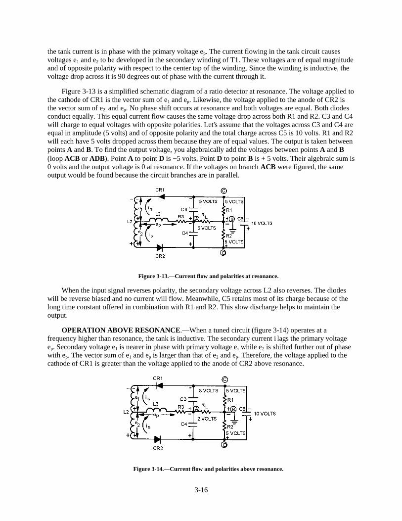
3-16
the tank current is in phase with the primary voltage ep. The current flowing in the tank circuit causesvoltages e1 and e2 to be developed in the secondary winding of T1. These voltages are of equal magnitudeand of opposite polarity with respect to the center tap of the winding. Since the winding is inductive, thevoltage drop across it is 90 degrees out of phase with the current through it.
Figure 3-13 is a simplified schematic diagram of a ratio detector at resonance. The voltage applied tothe cathode of CR1 is the vector sum of e1 and ep. Likewise, the voltage applied to the anode of CR2 isthe vector sum of e2 and ep. No phase shift occurs at resonance and both voltages are equal. Both diodesconduct equally. This equal current flow causes the same voltage drop across both R1 and R2. C3 and C4will charge to equal voltages with opposite polarities. Let’s assume that the voltages across C3 and C4 areequal in amplitude (5 volts) and of opposite polarity and the total charge across C5 is 10 volts. R1 and R2will each have 5 volts dropped across them because they are of equal values. The output is taken betweenpoints A and B. To find the output voltage, you algebraically add the voltages between points A and B(loop ACB or ADB). Point A to point D is −5 volts. Point D to point B is + 5 volts. Their algebraic sum is0 volts and the output voltage is 0 at resonance. If the voltages on branch ACB were figured, the sameoutput would be found because the circuit branches are in parallel.
Figure 3-13.—Current flow and polarities at resonance.
When the input signal reverses polarity, the secondary voltage across L2 also reverses. The diodeswill be reverse biased and no current will flow. Meanwhile, C5 retains most of its charge because of thelong time constant offered in combination with R1 and R2. This slow discharge helps to maintain theoutput.
OPERATION ABOVE RESONANCE.—When a tuned circuit (figure 3-14) operates at afrequency higher than resonance, the tank is inductive. The secondary current i lags the primary voltageep. Secondary voltage e1 is nearer in phase with primary voltage e, while e2 is shifted further out of phasewith ep. The vector sum of e1 and ep is larger than that of e2 and ep. Therefore, the voltage applied to thecathode of CR1 is greater than the voltage applied to the anode of CR2 above resonance.
Figure 3-14.—Current flow and polarities above resonance.
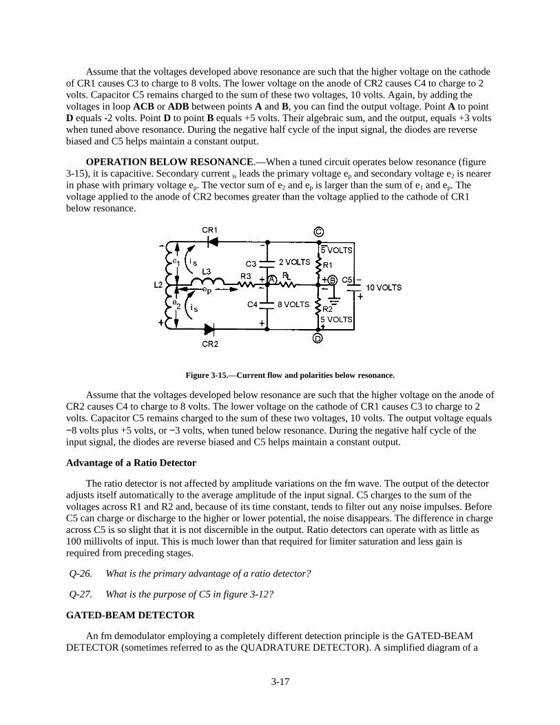
3-17
Assume that the voltages developed above resonance are such that the higher voltage on the cathodeof CR1 causes C3 to charge to 8 volts. The lower voltage on the anode of CR2 causes C4 to charge to 2volts. Capacitor C5 remains charged to the sum of these two voltages, 10 volts. Again, by adding thevoltages in loop ACB or ADB between points A and B, you can find the output voltage. Point A to pointD equals -2 volts. Point D to point B equals +5 volts. Their algebraic sum, and the output, equals +3 voltswhen tuned above resonance. During the negative half cycle of the input signal, the diodes are reversebiased and C5 helps maintain a constant output.
OPERATION BELOW RESONANCE.—When a tuned circuit operates below resonance (figure3-15), it is capacitive. Secondary current is leads the primary voltage ep and secondary voltage e2 is nearerin phase with primary voltage ep. The vector sum of e2 and ep is larger than the sum of e1 and ep. Thevoltage applied to the anode of CR2 becomes greater than the voltage applied to the cathode of CR1below resonance.
Figure 3-15.—Current flow and polarities below resonance.
Assume that the voltages developed below resonance are such that the higher voltage on the anode ofCR2 causes C4 to charge to 8 volts. The lower voltage on the cathode of CR1 causes C3 to charge to 2volts. Capacitor C5 remains charged to the sum of these two voltages, 10 volts. The output voltage equals−8 volts plus +5 volts, or −3 volts, when tuned below resonance. During the negative half cycle of theinput signal, the diodes are reverse biased and C5 helps maintain a constant output.
Advantage of a Ratio Detector
The ratio detector is not affected by amplitude variations on the fm wave. The output of the detectoradjusts itself automatically to the average amplitude of the input signal. C5 charges to the sum of thevoltages across R1 and R2 and, because of its time constant, tends to filter out any noise impulses. BeforeC5 can charge or discharge to the higher or lower potential, the noise disappears. The difference in chargeacross C5 is so slight that it is not discernible in the output. Ratio detectors can operate with as little as100 millivolts of input. This is much lower than that required for limiter saturation and less gain isrequired from preceding stages.
Q-26. What is the primary advantage of a ratio detector?
Q-27. What is the purpose of C5 in figure 3-12?
GATED-BEAM DETECTOR
An fm demodulator employing a completely different detection principle is the GATED-BEAMDETECTOR (sometimes referred to as the QUADRATURE DETECTOR). A simplified diagram of a
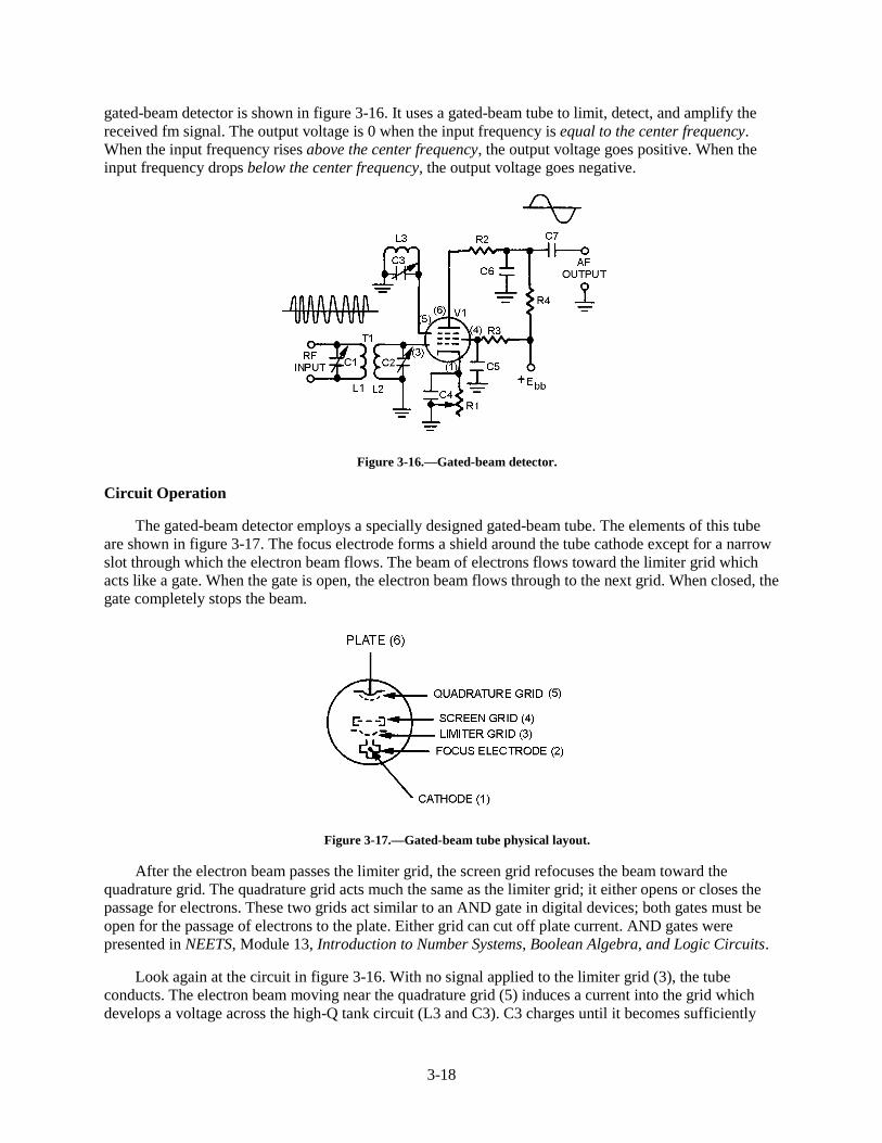
3-18
gated-beam detector is shown in figure 3-16. It uses a gated-beam tube to limit, detect, and amplify thereceived fm signal. The output voltage is 0 when the input frequency is equal to the center frequency.When the input frequency rises above the center frequency, the output voltage goes positive. When theinput frequency drops below the center frequency, the output voltage goes negative.
Figure 3-16.—Gated-beam detector.
Circuit Operation
The gated-beam detector employs a specially designed gated-beam tube. The elements of this tubeare shown in figure 3-17. The focus electrode forms a shield around the tube cathode except for a narrowslot through which the electron beam flows. The beam of electrons flows toward the limiter grid whichacts like a gate. When the gate is open, the electron beam flows through to the next grid. When closed, thegate completely stops the beam.
Figure 3-17.—Gated-beam tube physical layout.
After the electron beam passes the limiter grid, the screen grid refocuses the beam toward thequadrature grid. The quadrature grid acts much the same as the limiter grid; it either opens or closes thepassage for electrons. These two grids act similar to an AND gate in digital devices; both gates must beopen for the passage of electrons to the plate. Either grid can cut off plate current. AND gates werepresented in NEETS, Module 13, Introduction to Number Systems, Boolean Algebra, and Logic Circuits.
Look again at the circuit in figure 3-16. With no signal applied to the limiter grid (3), the tubeconducts. The electron beam moving near the quadrature grid (5) induces a current into the grid whichdevelops a voltage across the high-Q tank circuit (L3 and C3). C3 charges until it becomes sufficiently
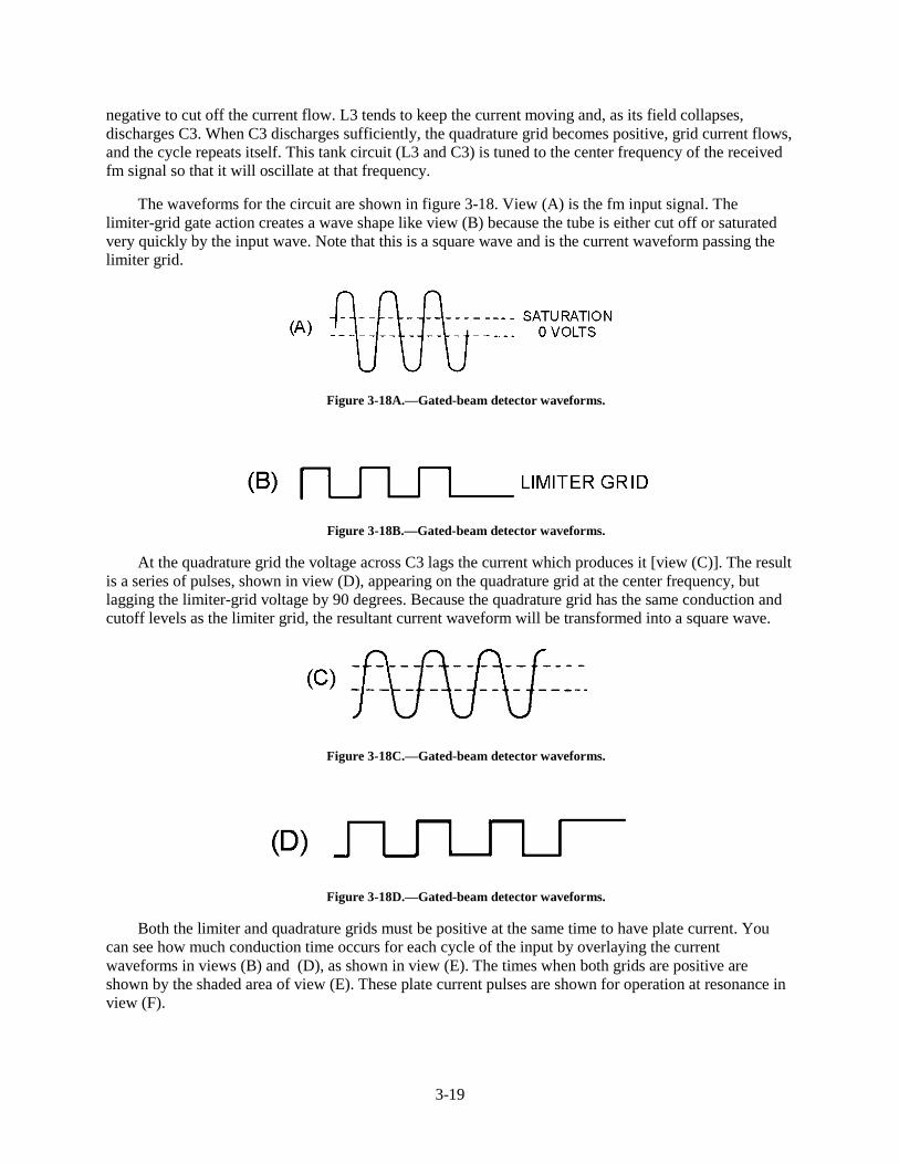
3-19
negative to cut off the current flow. L3 tends to keep the current moving and, as its field collapses,discharges C3. When C3 discharges sufficiently, the quadrature grid becomes positive, grid current flows,and the cycle repeats itself. This tank circuit (L3 and C3) is tuned to the center frequency of the receivedfm signal so that it will oscillate at that frequency.
The waveforms for the circuit are shown in figure 3-18. View (A) is the fm input signal. Thelimiter-grid gate action creates a wave shape like view (B) because the tube is either cut off or saturatedvery quickly by the input wave. Note that this is a square wave and is the current waveform passing thelimiter grid.
Figure 3-18A.—Gated-beam detector waveforms.
Figure 3-18B.—Gated-beam detector waveforms.
At the quadrature grid the voltage across C3 lags the current which produces it [view (C)]. The resultis a series of pulses, shown in view (D), appearing on the quadrature grid at the center frequency, butlagging the limiter-grid voltage by 90 degrees. Because the quadrature grid has the same conduction andcutoff levels as the limiter grid, the resultant current waveform will be transformed into a square wave.
Figure 3-18C.—Gated-beam detector waveforms.
Figure 3-18D.—Gated-beam detector waveforms.
Both the limiter and quadrature grids must be positive at the same time to have plate current. Youcan see how much conduction time occurs for each cycle of the input by overlaying the currentwaveforms in views (B) and (D), as shown in view (E). The times when both grids are positive areshown by the shaded area of view (E). These plate current pulses are shown for operation at resonance inview (F).

3-20
Figure 3-18E.—Gated-beam detector waveforms.
Figure 3-18F.—Gated-beam detector waveforms.
Now consider what happens with a deviation in frequency at the input. If the frequency increases, thefrequency across the quadrature tank also increases. Above resonance, the tank appears capacitive to theinduced current; voltage then lags the applied voltage by more than 90 degrees, as shown in view (G).Note in view (H) that the two grid signals have moved more out of phase and the average plate currentlevel has decreased.
Figure 3-18G.—Gated-beam detector waveforms.
Figure 3-18H.—Gated-beam detector waveforms.
As the input frequency decreases, the opposite action takes place. The two grid signals move more inphase, as shown in view (I), and the average plate current increases, as shown in view (J).
Figure 3-18I.—Gated-beam detector waveforms.
Figure 3-18J.—Gated-beam detector waveforms.
View (K) shows the resultant plate-current pulses when an fm signal is applied to a gated-beamdetector. Plate load resistor R4 and capacitor C6 form an integrating network which filters these pulses toform the sine-wave output.
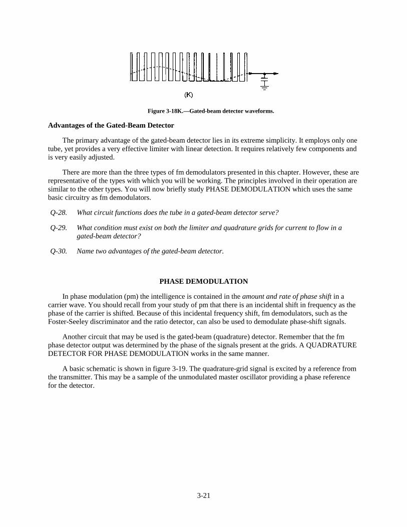
3-21
Figure 3-18K.—Gated-beam detector waveforms.
Advantages of the Gated-Beam Detector
The primary advantage of the gated-beam detector lies in its extreme simplicity. It employs only onetube, yet provides a very effective limiter with linear detection. It requires relatively few components andis very easily adjusted.
There are more than the three types of fm demodulators presented in this chapter. However, these arerepresentative of the types with which you will be working. The principles involved in their operation aresimilar to the other types. You will now briefly study PHASE DEMODULATION which uses the samebasic circuitry as fm demodulators.
Q-28. What circuit functions does the tube in a gated-beam detector serve?
Q-29. What condition must exist on both the limiter and quadrature grids for current to flow in agated-beam detector?
Q-30. Name two advantages of the gated-beam detector.
PHASE DEMODULATION
In phase modulation (pm) the intelligence is contained in the amount and rate of phase shift in acarrier wave. You should recall from your study of pm that there is an incidental shift in frequency as thephase of the carrier is shifted. Because of this incidental frequency shift, fm demodulators, such as theFoster-Seeley discriminator and the ratio detector, can also be used to demodulate phase-shift signals.
Another circuit that may be used is the gated-beam (quadrature) detector. Remember that the fmphase detector output was determined by the phase of the signals present at the grids. A QUADRATUREDETECTOR FOR PHASE DEMODULATION works in the same manner.
A basic schematic is shown in figure 3-19. The quadrature-grid signal is excited by a reference fromthe transmitter. This may be a sample of the unmodulated master oscillator providing a phase referencefor the detector.
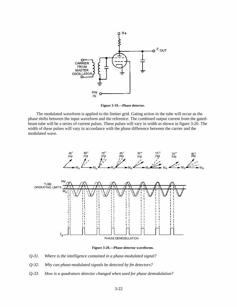
3-22
Figure 3-19.—Phase detector.
The modulated waveform is applied to the limiter grid. Gating action in the tube will occur as thephase shifts between the input waveform and the reference. The combined output current from the gated-beam tube will be a series of current pulses. These pulses will vary in width as shown in figure 3-20. Thewidth of these pulses will vary in accordance with the phase difference between the carrier and themodulated wave.
Figure 3-20.—Phase-detector waveforms.
Q-31. Where is the intelligence contained in a phase-modulated signal?
Q-32. Why can phase-modulated signals be detected by fm detectors?
Q-33. How is a quadrature detector changed when used for phase demodulation?
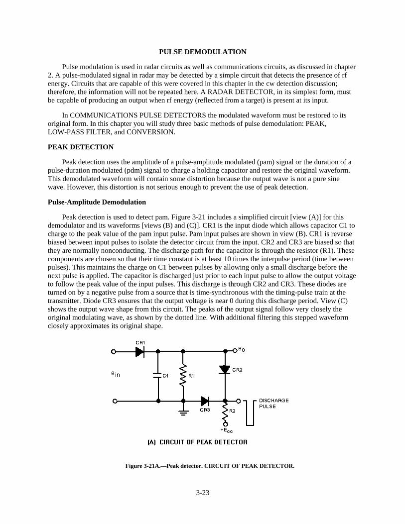
3-23
PULSE DEMODULATION
Pulse modulation is used in radar circuits as well as communications circuits, as discussed in chapter2. A pulse-modulated signal in radar may be detected by a simple circuit that detects the presence of rfenergy. Circuits that are capable of this were covered in this chapter in the cw detection discussion;therefore, the information will not be repeated here. A RADAR DETECTOR, in its simplest form, mustbe capable of producing an output when rf energy (reflected from a target) is present at its input.
In COMMUNICATIONS PULSE DETECTORS the modulated waveform must be restored to itsoriginal form. In this chapter you will study three basic methods of pulse demodulation: PEAK,LOW-PASS FILTER, and CONVERSION.
PEAK DETECTION
Peak detection uses the amplitude of a pulse-amplitude modulated (pam) signal or the duration of apulse-duration modulated (pdm) signal to charge a holding capacitor and restore the original waveform.This demodulated waveform will contain some distortion because the output wave is not a pure sinewave. However, this distortion is not serious enough to prevent the use of peak detection.
Pulse-Amplitude Demodulation
Peak detection is used to detect pam. Figure 3-21 includes a simplified circuit [view (A)] for thisdemodulator and its waveforms [views (B) and (C)]. CR1 is the input diode which allows capacitor C1 tocharge to the peak value of the pam input pulse. Pam input pulses are shown in view (B). CR1 is reversebiased between input pulses to isolate the detector circuit from the input. CR2 and CR3 are biased so thatthey are normally nonconducting. The discharge path for the capacitor is through the resistor (R1). Thesecomponents are chosen so that their time constant is at least 10 times the interpulse period (time betweenpulses). This maintains the charge on C1 between pulses by allowing only a small discharge before thenext pulse is applied. The capacitor is discharged just prior to each input pulse to allow the output voltageto follow the peak value of the input pulses. This discharge is through CR2 and CR3. These diodes areturned on by a negative pulse from a source that is time-synchronous with the timing-pulse train at thetransmitter. Diode CR3 ensures that the output voltage is near 0 during this discharge period. View (C)shows the output wave shape from this circuit. The peaks of the output signal follow very closely theoriginal modulating wave, as shown by the dotted line. With additional filtering this stepped waveformclosely approximates its original shape.
Figure 3-21A.—Peak detector. CIRCUIT OF PEAK DETECTOR.
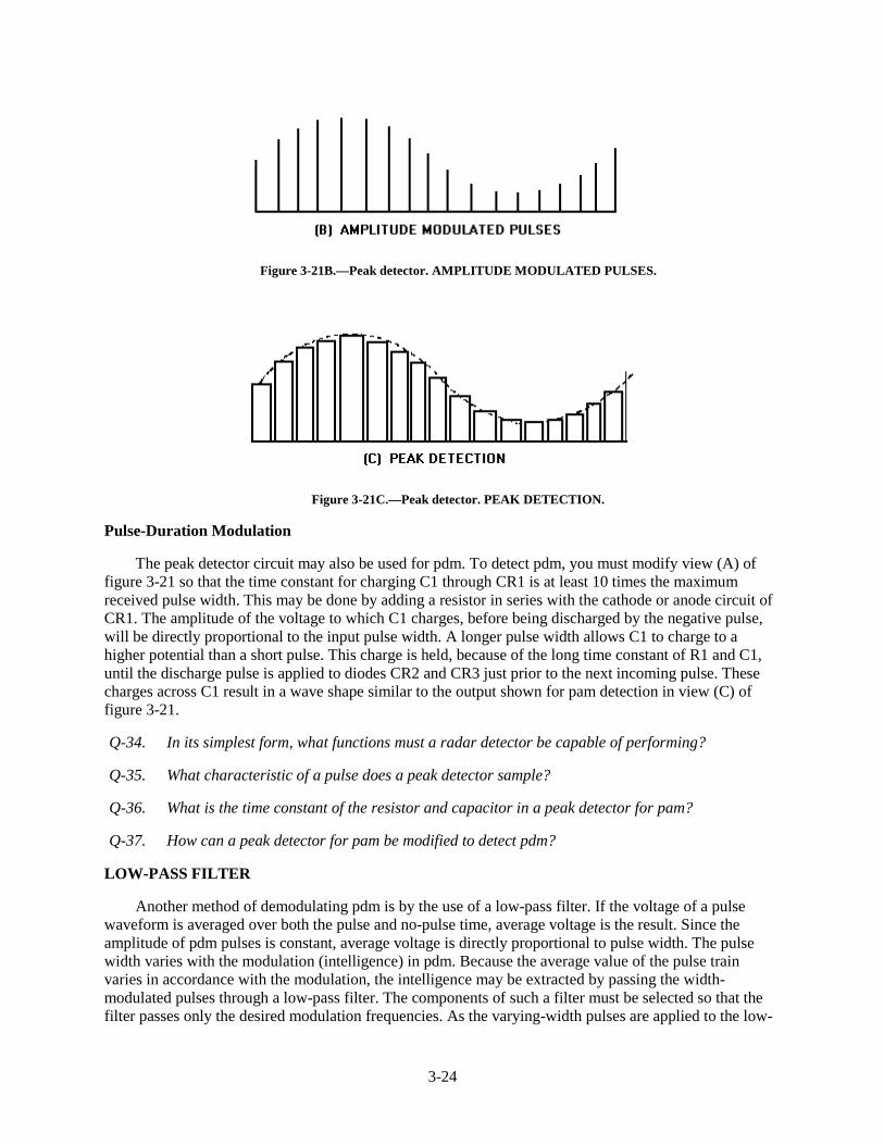
3-24
Figure 3-21B.—Peak detector. AMPLITUDE MODULATED PULSES.
Figure 3-21C.—Peak detector. PEAK DETECTION.
Pulse-Duration Modulation
The peak detector circuit may also be used for pdm. To detect pdm, you must modify view (A) offigure 3-21 so that the time constant for charging C1 through CR1 is at least 10 times the maximumreceived pulse width. This may be done by adding a resistor in series with the cathode or anode circuit ofCR1. The amplitude of the voltage to which C1 charges, before being discharged by the negative pulse,will be directly proportional to the input pulse width. A longer pulse width allows C1 to charge to ahigher potential than a short pulse. This charge is held, because of the long time constant of R1 and C1,until the discharge pulse is applied to diodes CR2 and CR3 just prior to the next incoming pulse. Thesecharges across C1 result in a wave shape similar to the output shown for pam detection in view (C) offigure 3-21.
Q-34. In its simplest form, what functions must a radar detector be capable of performing?
Q-35. What characteristic of a pulse does a peak detector sample?
Q-36. What is the time constant of the resistor and capacitor in a peak detector for pam?
Q-37. How can a peak detector for pam be modified to detect pdm?
LOW-PASS FILTER
Another method of demodulating pdm is by the use of a low-pass filter. If the voltage of a pulsewaveform is averaged over both the pulse and no-pulse time, average voltage is the result. Since theamplitude of pdm pulses is constant, average voltage is directly proportional to pulse width. The pulsewidth varies with the modulation (intelligence) in pdm. Because the average value of the pulse trainvaries in accordance with the modulation, the intelligence may be extracted by passing the width-modulated pulses through a low-pass filter. The components of such a filter must be selected so that thefilter passes only the desired modulation frequencies. As the varying-width pulses are applied to the low-

3-25
pass filter, the average voltage across the filter will vary in the same way as the original modulatingvoltage. This varying voltage will closely approximate the original modulating voltage.
CONVERSION
Pulse-position modulation (ppm), pulse-frequency modulation (pfm), and pulse-code modulation(pcm) are most easily demodulated by first converting them to either pdm or pam. After conversion thesepulses are demodulated using either peak detection or a low-pass filter. This conversion may be done inmany ways, but your study will be limited to the simpler methods.
Pulse-Position Modulation
Ppm can be converted to pdm by using a flip-flop circuit. (Flip flops were discussed inNEETS,Module 9,Introduction to Wave-Generation and Wave-Shaping Circuits.) Figure 3-22 shows thewaveforms for conversion of ppm to pdm. View (A) is the pulse-modulated pulse train and view (B) is aseries of reset trigger pulses. The trigger pulses must be synchronized with the unmodulated position ofthe ppm pulses, but with a fixed time delay from these pulses. As the position-modulated pulse is appliedto the flip-flop, the output is driven positive, as shown in view (C). After a period of time, the triggerpulse is again generated and drives the flip-flop output negative and the pulse ends. Because the ppmpulses are constantly varying in position with reference to the unmodulated pulses, the output of the flip-flop also varies in duration or width. This pdm signal can now be applied to one of the circuits that hasalready been discussed for demodulation.
Figure 3-22.—Conversion of ppm to pdm.
Pulse-frequency modulation is a variation of ppm and may be converted by the same method.
3-26
Pulse-Code Modulation
Pulse-code modulation can easily be decoded, provided the pulse-code groups have been transmittedin reverse order; that is, if the pulse with the lowest value is transmitted first, the pulse with the highestvalue is transmitted last. A circuit that will provide a constant value of current without regard to its load isknown as a current source. A current source is used to apply the pcm pulses to an RC circuit, such as thatshown in figure 3-23, view (A). The current source must be capable of supplying a linear charge to C1that will increase each time a pulse is applied if C1 is not allowed to discharge between pulses. In otherwords, if C1 charges to 16 volts during the period of one pulse, then each additional pulse increases thecharge by 16 volts. Thus, the cumulative value increases by 16 volts for each received pulse. This doesnot provide a usable output unless a resistor is chosen that allows C1 to discharge to one-half its valuebetween pulses. If only one pulse is received at T1, C1 charges to 16 volts and then begins to discharge.At T2 the charge has decayed to 8 volts and continues to decay unless another pulse is received. At T3 ithas a 4-volt charge and at T4 it only has a 2-volt charge. At the sampling time, a 1-volt charge remains;this charge corresponds to the binary-weighted pulse train of 0001. Now we will apply a pcm signalwhich corresponds to the binary-coded equivalent of 7 volts (0111) in figure 3-23, view (A). View (B) isthe pulse code that is received. Remember that the pulses are transmitted in reverse order. View (C) is theresponse curve of the circuit. At T1 the pulse corresponding to the least significant digit is applied and C1charges to 16 volts. C1 discharges between pulses until it reaches 8 volts at T2. At T2 another pulsecharges it to 24 volts. At T3, C1 has discharged through R1 to a value of 12 volts. The pulse at T3increases the charge on C1 by 16 volts to a total charge of 28 volts. At T4, C1 has discharged to one-halfits value and is at 14 volts. No pulse is present at T4 so C1 will not receive an additional charge. C1continues to discharge until T5 when it has reached 7 volts and is sampled to provide a pam pulse whichcan be peak detected. This sampled output corresponds to the original sampling of the analog voltage inthe modulation.
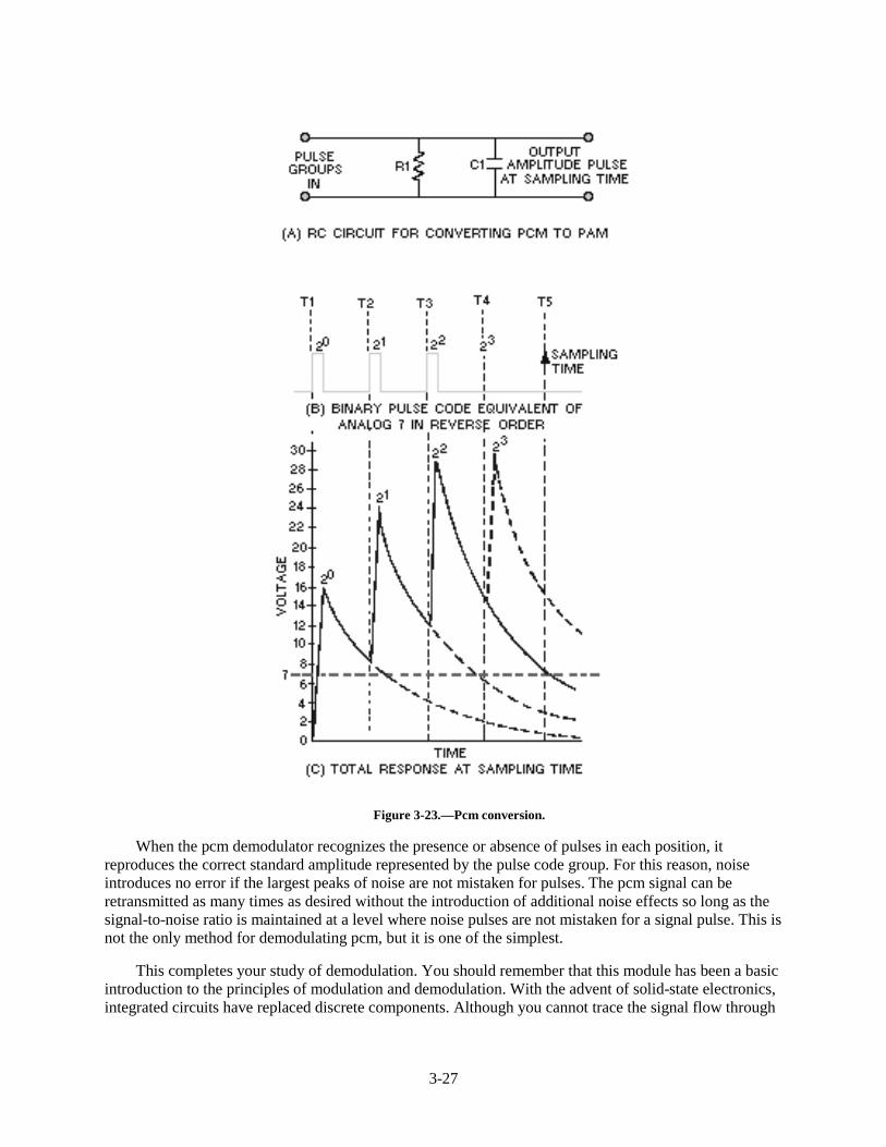
3-27
Figure 3-23.—Pcm conversion.
When the pcm demodulator recognizes the presence or absence of pulses in each position, itreproduces the correct standard amplitude represented by the pulse code group. For this reason, noiseintroduces no error if the largest peaks of noise are not mistaken for pulses. The pcm signal can beretransmitted as many times as desired without the introduction of additional noise effects so long as thesignal-to-noise ratio is maintained at a level where noise pulses are not mistaken for a signal pulse. This isnot the only method for demodulating pcm, but it is one of the simplest.
This completes your study of demodulation. You should remember that this module has been a basicintroduction to the principles of modulation and demodulation. With the advent of solid-state electronics,integrated circuits have replaced discrete components. Although you cannot trace the signal flow through
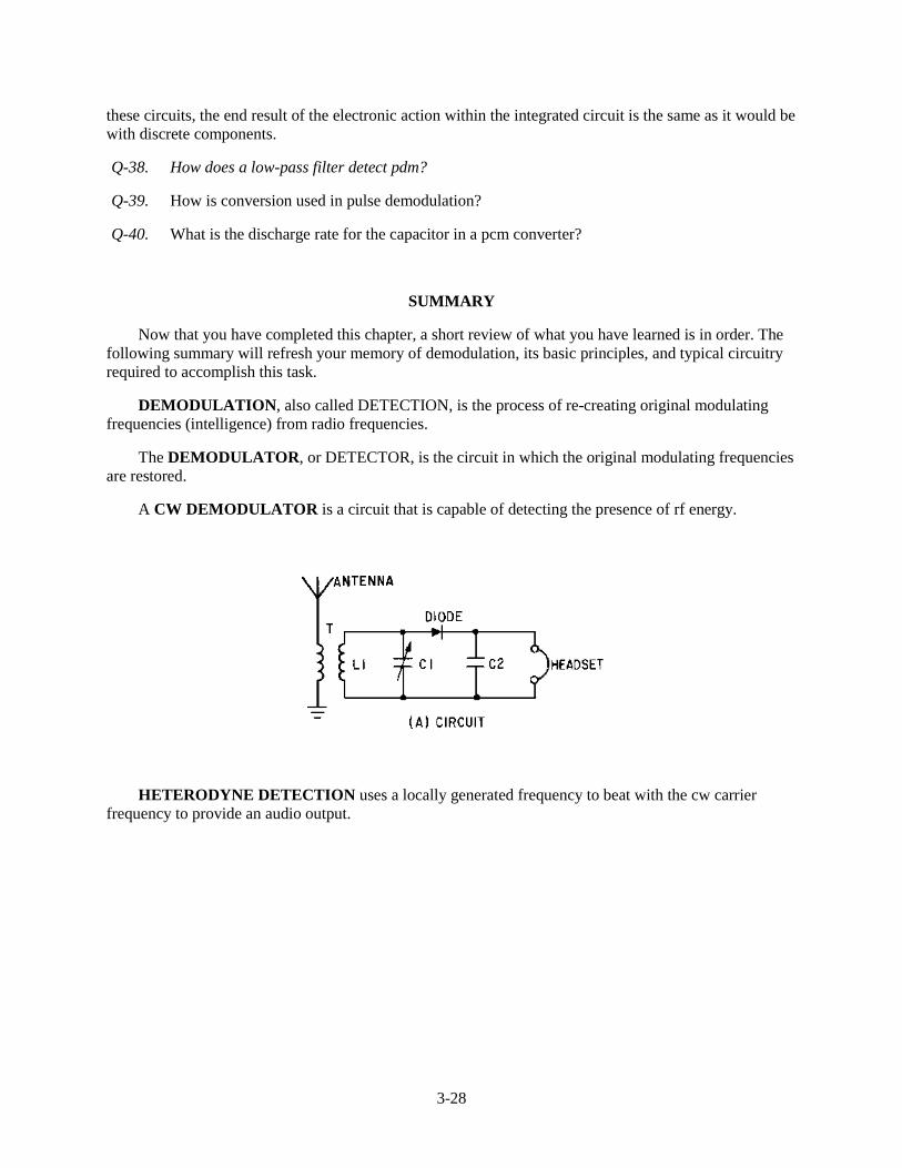
3-28
these circuits, the end result of the electronic action within the integrated circuit is the same as it would bewith discrete components.
Q-38. How does a low-pass filter detect pdm?
Q-39. How is conversion used in pulse demodulation?
Q-40. What is the discharge rate for the capacitor in a pcm converter?
SUMMARY
Now that you have completed this chapter, a short review of what you have learned is in order. Thefollowing summary will refresh your memory of demodulation, its basic principles, and typical circuitryrequired to accomplish this task.
DEMODULATION, also called DETECTION, is the process of re-creating original modulatingfrequencies (intelligence) from radio frequencies.
The DEMODULATOR, or DETECTOR, is the circuit in which the original modulating frequenciesare restored.
A CW DEMODULATOR is a circuit that is capable of detecting the presence of rf energy.
HETERODYNE DETECTION uses a locally generated frequency to beat with the cw carrierfrequency to provide an audio output.

3-29
The REGENERATIVE DETECTOR produces its own oscillations, heterodynes them with anincoming signal, and detects them.
The SERIES- (VOLTAGE-) DIODE DETECTOR has a rectifier diode that is in series with theinput voltage and the load impedance.
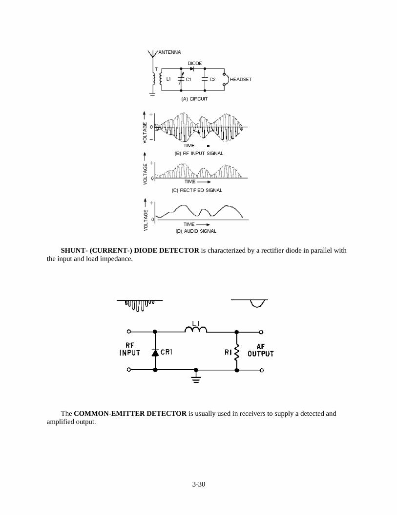
3-30
SHUNT- (CURRENT-) DIODE DETECTOR is characterized by a rectifier diode in parallel withthe input and load impedance.
The COMMON-EMITTER DETECTOR is usually used in receivers to supply a detected andamplified output.

3-31
The COMMON-BASE DETECTOR is an amplifying detector that is used in portable receivers.
The SLOPE DETECTOR is the simplest form of frequency detector. It is essentially a tank circuittuned slightly away from the desired fm carrier.
The FOSTER-SEELEY DISCRIMINATOR uses a double tuned rf transformer to convertfrequency changes of the received fm signal into amplitude variations of the rf wave.
The RATIO DETECTOR uses a double-tuned transformer connected so that the instantaneousfrequency variations of the fm input signal are converted into instantaneous amplitude variations.

3-32
The GATED-BEAM DETECTOR uses a specially-designed tube to limit, detect, and amplify thereceived fm signal.
PHASE DEMODULATION may be accomplished using a frequency discriminator or a quadraturedetector.
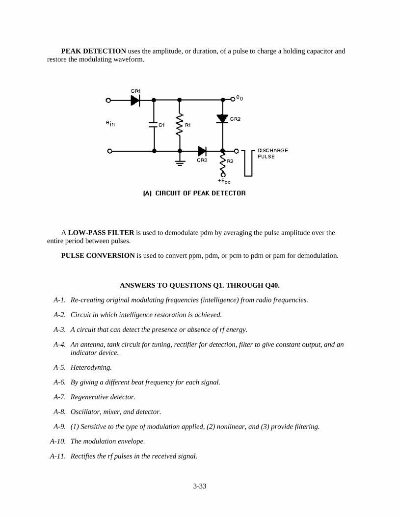
3-33
PEAK DETECTION uses the amplitude, or duration, of a pulse to charge a holding capacitor andrestore the modulating waveform.
A LOW-PASS FILTER is used to demodulate pdm by averaging the pulse amplitude over theentire period between pulses.
PULSE CONVERSION is used to convert ppm, pdm, or pcm to pdm or pam for demodulation.
ANSWERS TO QUESTIONS Q1. THROUGH Q40.
A-1. Re-creating original modulating frequencies (intelligence) from radio frequencies.
A-2. Circuit in which intelligence restoration is achieved.
A-3. A circuit that can detect the presence or absence of rf energy.
A-4. An antenna, tank circuit for tuning, rectifier for detection, filter to give constant output, and anindicator device.
A-5. Heterodyning.
A-6. By giving a different beat frequency for each signal.
A-7. Regenerative detector.
A-8. Oscillator, mixer, and detector.
A-9. (1) Sensitive to the type of modulation applied, (2) nonlinear, and (3) provide filtering.
A-10. The modulation envelope.
A-11. Rectifies the rf pulses in the received signal.
3-34
A-12. To filter the rf pulses and develop the modulating wave (intelligence) from the modulationenvelope.
A-13. The current-diode detector is in parallel with the input and load.
A-14. When the input voltage variations are too small to give a usable output from a series detector.
A-15. Emitter-base junction.
A-16. R1.
A-17. By the collector current flow through R4.
A-18. Emitter-base junction.
A-19. A diode detector followed by a stage of audio amplification.
A-20. C1 and R1.
A-21. Slope detector.
A-22. Converting frequency variations of received fm signals to amplitude variations.
A-23. A double-tuned tank circuit.
A-24. Rectify the rf voltage from the discriminator.
A-25. Inductive.
A-26. Suppresses amplitude noise without limiter stages.
A-27. It helps to maintain a constant circuit voltage to prevent noise fluctuations from interfering withthe output.
A-28. Limits, detects, and amplifies.
A-29. Both grids must be positively biased.
A-30. Extreme simplicity, few components, and ease of adjustment.
A-31. In the amount and rate of phase shift of the carrier wave.
A-32. Because of the incidental frequency shift that is caused while phase-shifting a carrier wave that issimilar to fm modulation.
A-33. The quadrature grid signal is excited by a reference from the transmitter.
A-34. Detecting the presence of rf energy.
A-35. Pulse amplitude or pulse duration.
A-36. At least 10 times the interpulse period.
A-37. By making the time constant for charging the capacitor at least 10 times the maximum receivedpulse width.
3-35
A-38. By averaging the value of the pulses over the period of the pulse-repetition rate.
A-39. Ppm, pfm, and pcm are converted to either pdm or pam for demodulation.
A-40. It will discharge to one-half its value between pulses.

AI-1
APPENDIX I
GLOSSARY
AMPLITUDE—Used to represent values of electrical current or voltage. The greater its height,the greater the value it represents.
AMPLITUDE MODULATION—Any method of varying the amplitude of an electromagneticcarrier frequency in accordance with the intelligence to be transmitted
ANGLE MODULATION—Modulation in which the angle of a sine-wave carrier is varied by amodulating wave.
AVERAGE POWER—The peak power value averaged over the pulse-repetition time.
BANDWIDTH—The section of the frequency spectrum that specific signals occupy.
BASE-INJECTION MODULATOR—Similar to control-grid modulator. Gain of a transistor isvaried by changing the bias on its base.
BLOCKED-GRID KEYING—A method of keying in which the bias is varied to turn platecurrent on and off.
BUFFER—A voltage amplifier used between the oscillator and power amplifier.
CARBON MICROPHONE—Microphone in which sound waves vary the resistance of a pile ofcarbon granules. May be single-button or double-button.
CARRIER FREQUENCY—The assigned transmitter frequency.
CARRIER—Radio-frequency sine wave.
CATHODE KEYING—A system in which the cathode circuit is interrupted so that neither gridcurrent nor plate current can flow.
CATHODE MODULATOR—Voltage on the cathode is varied to produce the modulationenvelope.
CHANNEL—Carrier frequency assignment usually with a fixed bandwidth.
COLLECTOR-INJECTION MODULATOR—Transistor equivalent of plate modulator.Modulating voltage is applied to collector circuit.
COMMON-BASE DETECTOR—An amplifying detector where detection occurs inemitter-base junction and amplification occurs at the output of the collector junction.
COMMON-EMITTER DETECTOR—Often used in receivers to supply detected andamplified output. The emitter-base junction acts as the detector.
COMPLEX WAVE—A wave composed of two or more parts.
CONTINUOUS-WAVE KEYING—The "on-off" keying of a carrier.
AI-2
CONTROL-GRID MODULATOR—Uses a variation of grid bias to vary the instantaneousplate voltage and current. The modulating signal is applied to the control grid.
CONVERSION—The process of changing ppm or pcm to pdm or pam to make them easier todemodulate.
CRYSTAL MICROPHONE—Uses the piezo-electric effect of crystalline materials to generatea voltage from sound waves.
CUSPS—Sharp phase reversals.
CW DEMODULATOR—A circuit that detects the presence of rf oscillations and converts theminto a useful form.
CYCLE—360 degree rotation of a vector generating a sine wave.
DEMODULATION—The removal of intelligence from a transmission medium.
DEMODULATION or DETECTION—The process of re-creating original modulating-frequency intelligence from the rf carrier.
DEMODULATOR or DETECTOR—A circuit in which demodulation or restoration of theoriginal intelligence is achieved.
DIODE DETECTOR—A simple type of crystal receiver.
DUTY CYCLE—The ratio of working time to total time for intermittently operated devices.
DYNAMIC MICROPHONE—A device in which sound waves move a coil of fine wire that ismounted on the back of a diaphragm and located in the magnetic field of a permanentmagnet.
EMITTER-INJECTION MODULATOR—The transistor equivalent of the cathode modulator.The gain is varied by changing the voltage on the emitter.
FIDELITY—The ability to faithfully re-produce the input in the output.
FINAL POWER AMPLIFIER (fpa)—The final stage of amplification in a transmitter.
FIXED SPARK GAP—A device used to discharge the pulse-forming network. A trigger pulseionizes the air between two contacts to initiate the discharge.
FOSTER-SEELEY DISCRIMINATOR—A circuit that uses a double-tuned rf transformer toconvert frequency variations in the received fm signal to amplitude variations. Also knownas a phase-shift discriminator.
FREQUENCY DEVIATION—The amount the frequency departs from the carrier frequency.
FREQUENCY MODULATION (fm)—Angle modulation in which the modulating signalcauses the carrier frequency to vary. The amplitude of the modulating signal determines howfar the frequency changes and the frequency of the modulating signal determines how fastthe frequency changes.
FREQUENCY MULTIPLIERS—Special rf power amplifiers that multiply the input frequency.
AI-3
FREQUENCY—The rate at which the vector that generates a sine wave rotates.
FREQUENCY-SHIFT KEYING (fsk)—Frequency modulation somewhat similar tocontinuous-wave (cw) keying in AM transmitters. The carrier is shifted between twodiffering frequencies by opening and closing a key.
GATED-BEAM DETECTOR—An fm demodulator that uses a special gated-beam tube tolimit, detect, and amplify the received fm signal. Also known as a quadrature detector.
HARMONIC FREQUENCIES—Integral multiples of a fundamental frequency
HETERODYNE DETECTION—The use of an af voltage to distinguish between availablesignals. The incoming cw signal is mixed with locally generated oscillations to give an afoutput.
HETERODYNING—Mixing two frequencies across a nonlinear impedance.
HIGH-LEVEL MODULATION—Modulation produced in the plate circuit of the last radiostage of the system.
INSTANTANEOUS AMPLITUDE—The amplitude at any given point along a sine wave at aspecific instant in time.
INTERMEDIATE POWER AMPLIFIER (ipa)—The amplifier between the oscillator andfinal power amplifier.
KEY CLICKS—Interference in the form of "clicks" or "thumps" caused by the suddenapplication or removal of power.
KEY-CLICK FILTERS—Filters used in keying systems to prevent key-click interference.
KEYING RELAYS—Relays used in high- power transmitters where the ordinary hand keycannot accommodate the plate current without excessive arcing.
LINEAR IMPEDANCE—An impedance in which a change in current through a device changesin direct proportion to the voltage applied to the device.
LOW-LEVEL MODULATION—Modulation produced in an earlier stage than the final.
LOW-PASS FILTER—A method of demodulating pdm by averaging the voltage over pulse andno-pulse time.
LOWER SIDEBAND—All difference frequencies below that of the carrier.
MACHINE KEYING—A method of cw keying using punched tape or other mechanical meansto key a transmitter.
MAGNETIC MICROPHONE—A microphone in which the sound waves vibrate a movingarmature. The armature consists of a coil wound on the armature and located between thepole pieces of a permanent magnet. The armature is mechanically linked to the diaphragm.
MARK—An interval during which a signal is present. Also the presence of an rf signal in cwkeying. The key-closed condition (presence of data) in communications systems.
AI-4
MASTER OSCILLATOR POWER AMPLIFIER (MOPA)—A transmitter in which theoscillator is isolated from the antenna by a power amplifier.
MICROPHONE—An energy converter that changes sound energy into electrical energy.
MODULATED WAVE—A complex wave consisting of a carrier and a modulating wave that istransmitted through space.
MODULATING WAVE—An information wave representing intelligence.
MODULATION FACTOR (M)—An indication of relative magnitudes of the rf carrier and theaudio-modulating signal.
MODULATION INDEX—The ratio of frequency deviation to the frequency of the modulatingsignal.
MODULATION—The ability to impress intelligence upon a transmission medium, such as radiowaves.
MODULATOR—The last audio stage in which intelligence is applied to the rf stage to modulatethe carrier.
MULTIPLICATION FACTOR—The number of times an input frequency is multiplied.
MULTIVIBRATOR MODULATOR—An astable multivibrator used to provide frequencymodulation by inserting the modulating af voltage in series with the base-return of themultivibrator transistors.
NEGATIVE ALTERNATION—That part of a sine wave that is below the reference level.
NONLINEAR DEVICE—A device in which the output does not rise and fall directly with theinput.
NONLINEAR IMPEDANCE—An impedance in which the resulting current through the deviceis not proportional to the applied voltage.
OVERMODULATION—A condition that exists when the peaks of the modulating signal arelimited.
PEAK AMPLITUDE—The maximum value above or below the reference line.
PEAK DETECTION—Detection that uses the amplitude of pam or the duration of pdm tocharge a holding capacitor and restore the original waveform.
PEAK POWER—The maximum value of the transmitted pulse.
PERCENT OF MODULATION—The degree of modulation defined in terms of the maximumpermissible amount of modulation.
PERIOD—The duration of a waveform.
PHASE MODULATION (pm)—Angle modulation in which the phase of the carrier iscontrolled by the modulating waveform. The amplitude of the modulating wave determinesthe amount of phase shift and the frequency of the modulation determines how often thephase shifts.

AI-5
PHASE or PHASE ANGLE—The angle that exists between the starting point of a vector and itsposition at that instant. An indication of how much of a cycle has been completed at anygiven instant in time.
PHASE-SHIFT DISCRIMINATOR—See Foster-Seeley discriminator.
PHASE-SHIFT KEYING—Similar to ON-OFF cw keying in AM systems and frequency-shiftkeying in fm systems. Each time a mark is received, the phase is reversed. No phase reversaltakes place when a space is received.
PLATE KEYING—A keying system in which the plate supply is interrupted.
PLATE MODULATOR—An electron-tube modulator in which the modulating voltage isapplied to the plate circuit of the tube.
POSITIVE ALTERNATION—That part of a sine wave that is above the reference line.
PULSE DURATION (pd)—The period of time during which a pulse is present.
PULSE MODULATION—A form of modulation in which one of the characteristics of a pulsetrain is varied.
PULSE WIDTH (pw)—The period of time during which a pulse occurs.
PULSE—A surge of plate current that occurs when a tube is momentarily saturated.
PULSE-AMPLITUDE MODULATION (pam)—Pulse modulation in which the amplitude ofthe pulses is varied by the modulating signal.
PULSE-CODE MODULATION (pcm)—A modulation system in which the standard values ofa quantized wave are indicated by a series of coded pulses.
PULSE-DURATION MODULATION (pdm)—Pulse modulation in which the time durationof the pulses is changed by the modulating signal.
PULSE-FORMING NETWORK (pfn)—A circuit used for storing energy. Essentially a shortsection of artificial transmission line.
PULSE-FREQUENCY MODULATION (pfm)—Pulse modulation in which the modulatingvoltage varies the repetition rate of a pulse train.
PULSE-POSITION MODULATION (ppm)—Pulse modulation in which the position of thepulses is varied by the modulating voltage.
PULSE-REPETITION FREQUENCY—The rate, in pulses per second, at which the pulsesoccur.
PULSE-REPETITION TIME (prt)—The total time for one complete pulse cycle of operation(rest time plus pulse width).
PULSE-TIME MODULATION (ptm)—Pulse modulation that varies one of the timecharacteristics of a pulse train (pwm, pdm, ppm, and pfm).
PULSE-WIDTH MODULATION (pwm)—Pulse modulation in which the duration of thepulses is varied by the modulating voltage.

AI-6
PULSING—Allowing oscillations to occur for a specific period of time only during selectedintervals.
QUANTIZED WAVE—A wave created by arbitrarily dividing the entire range of amplitude (orfrequency, or phase) values of an analog wave into a series of standard values. Each sampletakes the standard value nearest its actual value when modulated.
QUANTIZING NOISE—A distortion introduced by quantizing the signal.
RADAR DETECTOR—A detector which, in its simplest form, only needs to be capable ofproducing an output when rf energy (reflected from a target) is present at its input.
RATIO DETECTOR—A detector that uses a double-tuned transformer to convert theinstantaneous frequency variations of the fm input signal to instantaneous amplitudevariations.
RATIO OF TRANSMITTED POWERS—The power ratio (fsk verses AM) that expresses theoverall improvement of fsk transmission when compared to AM under rapid-fading andhigh-noise conditions.
REACTANCE TUBE—A tube connected in parallel with the tank circuit of an oscillator.Provides a signal that will either lag or lead the signal produced by the tank.
REACTANCE-TUBE MODULATOR—An fm modulator that uses a reactance tube in parallelwith the oscillator tank circuit.
REGENERATIVE DETECTOR—A detector circuit that produces its own oscillations,heterodynes them with an incoming signal, and detects them.
REST FREQUENCY—The carrier frequency during the constant-amplitude portions of a phasemodulation signal.
REST TIME (rt)—The time when there is no pulse or nonpulse.
ROTARY GAP—Similar to a mechanically driven switch. Used to discharge a pulse-formingnetwork.
SENSITIVITY OF A MICROPHONE—Efficiency of a microphone. Describes micro- phonepower delivered to a matched-impedance load as compared to the sound level beingconverted. Usually expressed in terms of the electrical power level.
SERIES-DIODE DETECTOR—The semiconductor diode in series with the input voltage andthe load impedance. Sometimes called a voltage-diode detector.
SHUNT—Means the same as parallel or to place in parallel with other components.
SHUNT-DIODE DETECTOR—A diode detector in which the diode is in parallel with the inputvoltage and the load impedance. Also known as a current detector because it operates withsmaller input levels.
SIGNAL DISTORTION—Any unwanted change to the signal.
SIGNIFICANT SIDEBANDS—Those sidebands with significantly large amplitude.
AI-7
SINE WAVE—The basic synchronous alternating waveform for all complex waveforms.
SLOPE DETECTOR—A tank circuit tuned to a frequency, either slightly above or below an fmcarrier frequency, that is used to detect intelligence.
SPACE—Absence of an rf signal in cw keying. Key-open condition or lack of data incommunications systems. Also a period of no signal.
SPARK-GAP MODULATOR—Modulator consists of a circuit for storing energy, a circuit forrapidly discharging the storage circuit (spark gap), a pulse transformer, and a power source.
SPECTRUM ANALYSIS—The display of electromagnetic energy arranged according towavelength or frequency.
SPLATTER—Unwanted sideband frequencies that are generated from overmodulation.
THYRATRON MODULATOR—An electronic switch that requires a low potential to turn iton.
TRANSMISSION MEDIUM—A means of transferring intelligence from point to point. Can bedescribed as light, smoke, sound, wirelines, or radio-frequency waves.
UPPER SIDEBAND—All of the sum frequencies above the carrier.
VARACTOR—A diode, or pn junction, that is designed to have a certain amount of capacitancebetween junctions.
VARACTOR FM MODULATOR—An fm modulator which uses avoltage-variablecapacitordiode (varactor).
VOLTAGE-DIODE DETECTOR—Series detector in which the crystal is in series with theinput voltage and the load impedance.
VECTOR—Mathematical method of showing both magnitude and direction.
WAVELENGTH—The physical dimension of a sine wave.


INDEX-1
MODULE 12 INDEX A Ac applied to linear and nonlinear impedances,
1-18 AM demodulation, 3-6 to 3-10 AM transmitter principles, 1-42 Amplitude, 1-7 Amplitude modulation, 1-1 to 1-62
amplitude-modulated systems, 1-26 AM transmitter principles, 1-42 amplitude modulation, 1-36 continuous wave (cw), 1-26 modulation systems, 1-54
heterodyning, 1-10 ac applied to linear and nonlinear
impedances, 1-18 combined linear and nonlinear
impedance, 1-17 linear impedance, 1-11 nonlinear impedance, 1-16 spectrum analysis, 1-25 two sine-wave generators and a
combination of linear and nonlinear impedances, 1-22
two sine-wave generators in linear circuits, 1-20
typical heterodyning circuit, 1-25 introduction to modulation principles, 1-1 sine-wave characteristics, 1-2
amplitude, 1-7 frequency, 1-7 generation of sine waves, 1-3 period, 1-7 phase, 1-7 wavelength, 1-8
summary, 1-62 Angle and pulse modulation, 2-1
angle modulation, 2-2 basic modulator, 2-25 frequency-modulation systems, 2-2 frequency-shift keying, 2-2 modulation index, 2-23 phase modulation, 2-21 phase-shift keying, 2-26
Angle and pulse modulation—Continued introduction, 2-1 pulse modulation, 2-29
characteristics, 2-29 communications pulse modulators,
2-40 pulse timing, 2-32 radar modulation, 2-38 spark-gap modulator, 2-38 thyratron modulator, 2-39
summary, 2-52 B Basic modulator, 2-25 C Characteristics, pulse modulation, 2-29 Combined linear and nonlinear impedance,
1-17 Common-base detector, 3-10 Common-emitter detectors, 3-9 Communications pulse modulators, 2-40 Continuous wave (cw), 1-26 Continuous-wave demodulation, 3-2 Conversion, 3-25 D Demodulation, 3-1
AM demodulation, 3-6 common-base detector, 3-10 common-emitter detectors, 3-9 diode detectors, 3-6
continuous-wave demodulation, 3-2 heterodyne detection, 3-3 regenerative detector, 3-5
fm demodulation, 3-10 Foster-Seeley discriminator, 3-12 gated-beam detector, 3-17 ratio detector, 3-15 slope detection, 3-11
introduction, 3-1
INDEX-2
Demodulation—Continued phase demodulation, 3-21 pulse demodulation, 3-23
conversion, 3-25 low-pass filter, 3-24 peak detection, 3-23
summary, 3-28 Diode detectors, 3-6 F Fm demodulation, 3-10 Foster-Seeley discriminator, 3-12 Frequency, 1-7 Frequency-modulation systems, 2-2 Frequency-shift keying, 2-2 G Gated-beam detector, 3-17 Generation of sine waves, 1-3 Glossary, AI-1 to AI-7 H Heterodyne detection, 3-3 Heterodyning, 1-10 L Learning objectives, 1-1, 2-1, 3-1 Linear impedance, 1-11 Low-pass filter, 3-24 M Modulation index, 2-23 Modulation principles, introduction to, 1-1 Modulation systems, 1-54
N Nonlinear impedance, 1-16 P Peak detection, 3-23 Period, 1-7 Phase, 1-7 Phase demodulation, 3-21 Phase modulation, 2-21 Phase-shift keying, 2-26 Pulse and angle modulation, 2-1 Pulse demodulation, 3-23 R Radar modulation, 2-38 Ratio detector, 3-15 Regenerative detector, 3-5 S Sine-wave characteristics, 1-2 Slope detection, 3-11 Spark-gap modulator, 2-38 Spectrum analysis, 1-25 T Thyratron modulator, 2-39 Timing, pulse, 2-32 Two sine-wave generators and a combination
of linear and nonlinear impedances, 1-22 Two sine-wave generators, in linear circuits,
1-20 Typical heterodyning circuit, 1-25 W Wavelength, 1-8

Assignment Questions
Information: The text pages that you are to study areprovided at the beginning of the assignment questions.


1
ASSIGNMENT 1
Textbook assignment: Chapter 1, “Amplitude Modulation,” pages 1-1 through 1-75. _________________________________________________________________________________
1-1. The action of impressing intelligence upon a transmission medium is referred to as
1. modulating 2. demodulating 3. heterodyning 4. wave generating
1-2. You can communicate with others using which of the following transmissions mediums?
1. Light 2. Wire lines 3. Radio waves 4. Each of the above
1-3. When you use a vector to indicate force in a diagram, what do (a) length and (b) arrowhead position indicate?
1. (a) Magnitude (b) direction 2. (a) Magnitude (b) frequency 3. (a) Phase (b) frequency 4. (a) Phase (b) direction
1-4. Vectors are used to show which of the following characteristics of a sine wave?
1. Fidelity 2. Amplitude 3. Resonance 4. Distortion
1-5. A rotating coil in the uniform magnetic field between two magnets produces a sine wave. It is called a sine wave because the voltage depends on which of the following factors?
1. The number of turns in the coil 2. The speed at which the coil is rotating 3. The angular position of the coil in the
magnetic field 4. Each of the above
1-6. The trigonometric relationship for the sine of an angle in a right triangle is figured using which of the following ratios?
1. Opposite side ÷ hypotenuse 2. Adjacent side ÷ hypotenuse 3. Hypotenuse ÷ opposite side 4. Hypotenuse ÷ adjacent side
1-7. The part of a sine wave that is above the voltage reference line is referred to as the
1. peak amplitude 2. positive alternation 3. negative alternation 4. instantaneous amplitude
1-8. The degree to which a cycle has been completed at any given instant is referred to as the
1. phase 2. period 3. frequency 4. amplitude

2
1-9. The frequency of the sine wave is determined by which of the following sine-wave factors?
1. The maximum voltage 2. The rate at which the vector rotates 3. The number of degrees of vector
rotation 4. Each of the above
1-10. Which of the following mathematical relationships do you use to figure the period of a sine wave?
1.
3.
2.
4.
1-11. Which of the following Greek letters is
the symbol for wavelength?
1. θ 2. ϑ 3. λ 4. ω
1-12. Which of the following waveform characteristics determines the wavelength of a sine wave?
1. Phase 2. Period 3. Amplitude 4. Phase Angle
1-13. An electromagnetic wavefront moves through free space at approximately what speed in meters per second?
1. 3,000,000 2. 30,000,000 3. 300,000,000 4. 3,000,000,000
1-14. What is the wavelength of a 1.5 MHz frequency?
1. 100 meters 2. 200 meters 3. 300 meters 4. 400 meters
1-15. As the frequency of a signal is increased, what change can be noted about its wavelength?
1. It decreases 2. It increases 3. It remains the same
1-16. The ability of a circuit to faithfully reproduce the input signal in the output is known by what term?
1. Fidelity 2. Fluctuation 3. Directivity 4. Discrimination
1-17. In rf communications, modulation impresses information on which of the following types of waves?
1. Carrier wave 2. Complex wave 3. Modulated wave 4. Modulating wave
1-18. Which of the following types of modulation is a form of amplitude modulation?
1. Angle 2. Phase 3. Frequency 4. Continuous-wave
3
1-19. With a sine-wave input, how will the output compare to the input in (a) a linear circuit and (b) a nonlinear circuit?
1. (a) Proportional
(b) proportional
2. (a) Proportional (b) not proportional
3. (a) Not proportional (b) not proportional
4. (a) Not proportional (b) proportional
1-20. What effect, if any, does a nonlinear
device have on a sine wave?
1. It amplifies without distortion 2. It attenuates without distortion 3. It generates harmonic frequencies 4. None
1-21. For the heterodyning action to occur in a circuit, (a) what number of frequencies must be present and (b) to what type of circuit must they be applied?
1. (a) Two (b) linear 2. (a) Two (b) nonlinear 3. (a) Three (b) nonlinear 4. (a) Three (b) linear
1-22. Spectrum analysis is used to view which of the following characteristics of an rf signal?
1. Phase 2. Bandwidth 3. Modulating wave 4. Modulation envelope
1-23. The method of rf communication that uses either the presence or absence of a carrier in a prearranged code is what type of modulation?
1. Pulse modulation 2. Amplitude modulation 3. Continuous-wave modulation 4. Pulse-time modulation
1-24. What is the purpose of the key in a cw transmitter?
1. It generates the rf oscillations 2. It heterodynes the rf oscillations 3. It controls the rf output 4. It amplifies the rf signal
1-25. To ensure frequency stability in a cw transmitter, you should NOT key what circuit?
1. The mixer 2. The detector 3. The oscillator 4. The rf amplifier
1-26. When keying a high-power transmitter, what component should you use to reduce the shock hazard?
1. A coil 2. A relay 3. A resistor 4. A capacitor
1-27. Interference detected by a receiver is often caused by the application and removal of power in nearby transmitters. This interference can be prevented by using what type of circuit in such transmitters?
1. Power filter 2. On-off filter 3. Key-click filter 4. Rf detector filter
1-28. Transmitter machine keying was developed for which of the following purposes?
1. To increase the speed of
communications 2. To make communications more
intelligible 3. To reduce interference 4. Each of the above
4
1-29. Which of the following advantages is a benefit of cw communications?
1. Wide bandwidth 2. Fast transmission 3. Long-range operation 4. Each of the above
1-30. To prevent a transmitter from being loaded unnecessarily, where should you connect the antenna?
1. At the oscillator input 2. At the oscillator output 3. At the power-amplifier input 4. At the power-amplifier output
1-31. Amplifier tubes are added to the output of a transmitter for which of the following reasons?
1. To increase power 2. To increase frequency 3. To increase stability 4. To increase selectivity
1-32. Which of the following combinations of frequency multiplier stages will produce a total multiplication factor of 72?
1. 36, 36 2. 4, 3, 3, 2 3. 4, 4, 3, 2 4. 18, 18, 18, 18
1-33. To change sound energy into electrical energy, which of the following devices should you use?
1. A speaker 2. A microphone 3. An amplifier 4. An oscillator
1-34. Which of the following is the schematic symbol for a microphone?
1.
3.
2.
4.
1-35. What component in a carbon microphone converts a dc voltage into a varying current?
1. Button 2. Diaphragm 3. Transformer 4. Carbon granules
1-36. The action of the double-button carbon microphone is similar to which of the following electronic circuits?
1. A limiter 2. An oscillator 3. A voltage doulber 4. A push-pull amlifier
1-37. A carbon microphone has which of the following advantages over other types of microphones?
1. Ruggedness 2. Sensitivity 3. Low output voltage 4. Frequency response
1-38. The voltage produced by mechanical stress placed on certain crystals is a result of which of the following effects?
1. Hall 2. Acoustic 3. Electrostatic 4. Piezoelectric
5
1-39. If you require a microphone that is lightweight, has high sensitivity, is rugged, requires no external voltage, can withstand temperature, vibration, and moisture extremes, and has a uniform frequency response of 40 to 15,000 hertz, which of the following types of microphones should you select?
1. Carbon 2. Crystal 3. Dynamic 4. Electrostatic
1-40. What component in a magnetic microphone causes the lines of flux to alternate?
1. The coil 2. The magnet 3. The diaphragm 4. The armature
1-41. What are the two major sections of an AM transmitter?
1. Audio frequency unit and radio
frequency unit 2. Audio frequency unit and master
oscillator 3. Audio frequency unit and final power
amplifier 4. Audio frequency unit and
intermediate power amplifier
1-42. The intermediate power amplifier serves what function in a transmitter?
1. It generates the carrier 2. It modulates the carrier 3. It increases the frequency of the
signal 4. It increases the power level of the
signal
1-43. The final audio stage in an AM transmitter is the
1. mixer 2. modulator 3. multipler 4. multiplexer
1-44. The vertical axis on a frequency-spectrum graph represents which of the following waveform characteristics?
1. Phase 2. Duration 3. Frequency 4. Amplitude
1-45. When a 500-hertz signal modulates a 1-megahertz carrier, the 1-megahertz carrier and what two other frequencies are transmitted?
1. 500 and 999,500 hertz 2. 500 and 1,000,500 hertz 3. 999,500 and 1,500,000 hertz 4. 999,500 and 1,000,500 hertz
1-46. If 750 hertz modulates a 100-kilohertz carrier, what would the upper-sideband frequency be?
1. 99,250 hertz 2. 100,000 hertz 3. 100,500 hertz 4. 100,750 hertz
1-47. In an AM wave, where is the audio intelligence located?
1. In the carrier frequency 2. In the spacing between the sideband
frequencies 3. In the spacing between the carrier and
sideband frequencies 4. In the sideband frequencies
6
1-48. What determines the bandwidth of an AM wave?
1. The carrier frequency 2. The number of sideband frequencies 3. The lowest modulating frequency 4. The highest modulating frequency
1-49. If an 860-kilohertz AM signal is modulated by frequencies of 5 and 10 kilohertz, what is the bandwidth?
1. 5 kilohertz 2. 10 kilohertz 3. 15 kilohertz 4. 20 kilohertz
1-50. If a 1-megahertz signal is modulated by frequencies of 50 and 75 kilohertz, what is the resulting maximum frequency range?
1. 925,000 to 1,000,000 hertz 2. 925,000 to 1,075,000 hertz 3. 975,000 to 1,025,000 hertz 4. 1,000,000 to 1,075,000 hertz
1-51. If an rf carrier is 100 percent AM-modulated, what will be the rf output when the modulating signal is (a) at its negative peak and (b) at its positive peak?
(a) 0 1. (b) 2 times the amplitude of the
unmodulated carrier 2. (a) 0
(b) 1/2 the amplitude of the unmodulated carrier
(a) 1/2 the amplitude of the unmodulated carrier
3.
(b) 1/2 the amplitude of the unmodulated carrier
(a) 1/2 the amplitude of the unmodulated carrier
4.
(b) 2 times the amplitude of the unmodulated carrier
1-52. In an AM signal that is 100 percent modulated, what maximum voltage value is present in each sideband?
1. 1/4 the carrier voltage 2. 1/2 the carrier voltage 3. 3/4 the carrier voltage 4. Same as the carrier voltage
1-53. Overmodulation of an AM signal will have which, if any, of the following effects on the bandwidth?
1. It will increase 2. It will decrease 3. It will remain the same
1-54. In a carrier wave with a peak amplitude of 400 volts and a peak modulating voltage of 100 volts, what is the modulation factor?
1. 0.15 2. 0.25 3. 0.45 4. 0.55
1-55. The percent of modulation for a modulated carrier wave is figured using which of the following formulas?
1.
3.
2.
4.
1-56. Modulation produced in the plate circuit of the last radio stage of a system is known by what term?
1. Low-level modulation 2. High-level modulation 3. Final-amplifier modulation 4. Radio frequency modulation
7
1-57. Which, if any, of the following advantages is a primary benefit of plate modulation?
1. It operates at low efficiency 2. It operates at low power levels 3. It operates with high efficiency 4. None of the above
1-58. A final rf power amplifier biased for plate modulation operates in what class of operation?
1. A 2. B 3. AB 4. C
1-59. Heterodyning action in a plate modulator takes place in what circuit?
1. Grid 2. Plate 3. Screen 4. Cathode
1-60. A plate modulator produces a modulated rf output by controlling which of the following voltages?
1. Plate voltage 2. Cathode voltage 3. Grid-bias voltage 4. Grid-input voltage
1-61. To achieve 100-percent modulation in a plate modulator, what maximum voltage must the modulator tube be capable of providing to the final power amplifier (fpa)?
1. Twice the fpa plate voltage 2. The same as the fpa plate voltage 3. Three times the fpa plate voltage 4. Half the fpa plate voltage
1-62. In a plate modulator, with no modulation, how will the plate current of the final rf amplifier appear on a scope?
1. A series of pulses at the carrier
frequency 2. A series of pulses at twice the carrier
frequency 3. A series of pulses at 1/4 the carrier
frequency 4. A series of pulses at 1/2 the carrier
frequency
1-63. In the collector-injection modulator, af and rf are heterodyned by injecting the rf into (a) what circuit and the af into (b) what circuit?
1. (a) Base (b) collector 2. (a) Base (b) emitter 3. (a) Emitter (b) collector 4. (a) Emitter (b) base
1-64. Plate- and collector-injection modulators are the most commonly used modulators for which of the following reasons?
1. The rf amplifier stages can be
operated class C for linearity 2. The rf amplifier stages can be
operated class C for maximum efficiency
3. They require small amounts of audio power
4. They require large amounts of audio power
1-65. A control-grid modulator would be used
in which of the following situations?
1. In extremely high-power, wideband equipment where high-level modulation is difficult to achieve
2. In cases where the use of a minimum of audio power is desired
3. In portable and mobile equipment to reduce size and power requirements
4. Each of the above
8
1-66. Which of the following inputs is/are applied to the grid of a control-grid modulator?
1. Rf 2. Af 3. Dc bias 4. Each of the above
1-67. Excessive modulating signal levels have which, if any, of the following effects on a control-grid modulator?
1. They increase output. amplitude 2. They decrease output amplitude 3. They create distortion 4. None
1-68. Compared to a plate modulator, the control-grid modulator has which of the following advantages?
1. It is more efficient 2. It has less distortion 3. It requires less power from the
modulator 4. It requires less power from the
amplifier
1-69. The control-grid modulator is similar to which of the following modulator circuits?
1. Plate 2. Cathode 3. Base-injection 4. Emitter-injection
Figure 1A.—Modulator circuit.
IN ANSWERING QUESTIONS 1-70 THROUGH 1-72, REFER TO FIGURE 1A.
1-70. What components in the circuit establish
the bias for Q1?
1. R1 and R2 2. R2 and R3 3. R1 and R3
1-71. The rf voltage in the circuit is applied at (a) what points and the af voltage is applied at (b) what points?
1. (a) A and B (b) C and D 2. (a) C and D (b) A and B 3. (a) C and D (b) E and F 4. (a) E and F (b) C and D
1-72. What components develop the rf modulation envelope?
1. C1 and R1 2. C2 and R1 3. C3 and R3 4. C4 and L1
9
1-73. A cathode modulator is used in which of the following situations?
1. When rf power is unlimited and
distortion can be tolerated 2. When rf power is limited and
distortion cannot be tolerated 3. When af power is unlimited and
distortion can be tolerated 4. When af power is limited and
distortion cannot be tolerated 1-74. In a cathode modulator, the modulating
voltage is in series with which of the following voltages?
1. The grid voltage only 2. The plate voltage only 3. Both the grid and plate voltages 4. The cathode voltage only
Figure 1B.—Emitter-injection modulator.
IN ANSWERING QUESTION 1-75, REFER TO FIGURE 1B. 1-75. In the circuit, what components develop
the modulation envelope?
1. Q1 2. C2 and R1 3. C3 and R3 4. C4 and L1
10
ASSIGNMENT 2
Textbook assignment: Chapter 2, “Angle and Pulse Modulation,” pages 2-1 through 2-64.___________________________________________________________________________________
2-1. Frequency-shift keying resembles whattype of AM modulation?
1. CW modulation2. Analog AM modulation3. Plate modulation4. Collector-injection modulation
2-2. Frequency-shift keying is generated usingwhich of the following methods?
1. By shifting the frequency of anoscillator at an af rate
2. By shifting the frequency of anoscillator at an rf rate
3. By keying an af oscillator at an rf rate4. By keying an af oscillator at an af rate
2-3. In a frequency-shift keyed signal, where isthe intelligence contained?
1. In the duration of the rf energy2. In the frequency of the rf energy3. In the amplitude of the rf energy4. In the spacing between bursts of rf
energy
2-4. If an fsk transmitter has a MARKfrequency of 49.575 kilohertz and aSPACE frequency of 50.425 kilohertz,what is the assigned channel frequency?
1. 49 kilohertz2. 49.575 kilohertz3. 50 kilohertz4. 50.425 kilohertz
2-5. Fsk is NOT affected by noise interferencefor which of the following reasons?
1. Noise is outside the bandwidth of anfsk signal
2. Fsk does not rely on the amplitude ofthe transmitted signal to carryintelligence
3. The wide bandwidth of an fsk signalprevents noise interference
4. Each of the above
2-6. In an fsk transmitter, what stage is keyed?
1. The oscillator2. The power supply3. The power amplifier4. The buffer amplifier
2-7. When the amount of oscillator frequencyshift in an fsk transmitter is determined,which of the following factors must beconsidered?
1. The number of buffer amplifiers2. The transmitter power output3. The frequency multiplication factor for
the transmitter amplifiers4. The oscillator rest frequency
2-8. In an fsk transmitter with a doubler and atripler stage, the desired frequency shift is1,200 hertz. To what maximum amount isthe oscillator frequency shift limited?
1. 60 hertz2. 100 hertz3. 120 hertz4. 200 hertz
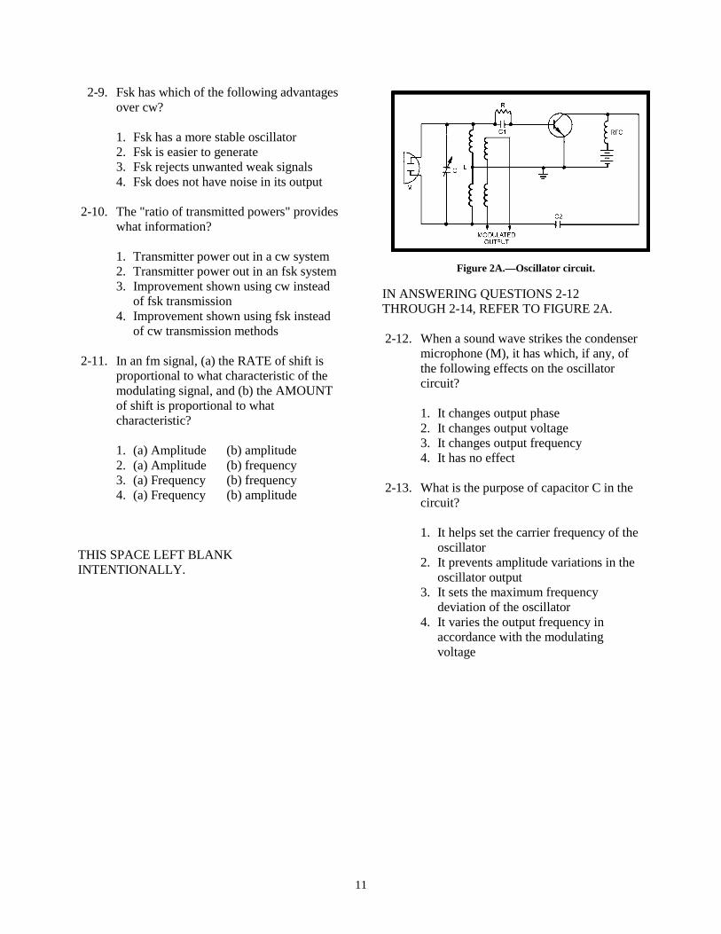
11
2-9. Fsk has which of the following advantagesover cw?
1. Fsk has a more stable oscillator2. Fsk is easier to generate3. Fsk rejects unwanted weak signals4. Fsk does not have noise in its output
2-10. The "ratio of transmitted powers" provideswhat information?
1. Transmitter power out in a cw system2. Transmitter power out in an fsk system3. Improvement shown using cw instead
of fsk transmission4. Improvement shown using fsk instead
of cw transmission methods
2-11. In an fm signal, (a) the RATE of shift isproportional to what characteristic of themodulating signal, and (b) the AMOUNTof shift is proportional to whatcharacteristic?
1. (a) Amplitude (b) amplitude2. (a) Amplitude (b) frequency3. (a) Frequency (b) frequency4. (a) Frequency (b) amplitude
THIS SPACE LEFT BLANKINTENTIONALLY.
Figure 2A.—Oscillator circuit.
IN ANSWERING QUESTIONS 2-12THROUGH 2-14, REFER TO FIGURE 2A.
2-12. When a sound wave strikes the condensermicrophone (M), it has which, if any, ofthe following effects on the oscillatorcircuit?
1. It changes output phase2. It changes output voltage3. It changes output frequency4. It has no effect
2-13. What is the purpose of capacitor C in thecircuit?
1. It helps set the carrier frequency of theoscillator
2. It prevents amplitude variations in theoscillator output
3. It sets the maximum frequencydeviation of the oscillator
4. It varies the output frequency inaccordance with the modulatingvoltage
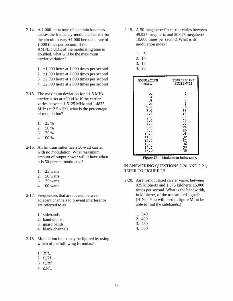
12
2-14. A 1,000-hertz tone of a certain loudnesscauses the frequency-modulated carrier forthe circuit to vary ±1,000 hertz at a rate of1,000 times per second. If theAMPLITUDE of the modulating tone isdoubled, what will be the maximumcarrier variation?
1. ±1,000 hertz at 1,000 times per second2. ±1,000 hertz at 2,000 times per second3. ±2,000 hertz at 1,000 times per second4. ±2,000 hertz at 2,000 times per second
2-15. The maximum deviation for a 1.5 MHzcarrier is set at ±50 kHz. If the carriervaries between 1.5125 MHz and 1.4875MHz (±12.5 kHz), what is the percentageof modulation?
1. 25 %2. 50 %3. 75 %4. 100 %
2-16. An fm transmitter has a 50-watt carrierwith no modulation. What maximumamount of output power will it have whenit is 50-percent modulated?
1. 25 watts2. 50 watts3. 75 watts4. 100 watts
2-17. Frequencies that are located betweenadjacent channels to prevent interferenceare referred to as
1. sidebands2. bandwidths3. guard bands4. blank channels
2-18. Modulation index may be figured by usingwhich of the following formulas?
1. 2f/fm
2. fm/2f3. fm/∆f4. ∆f/fm
2-19. A 50-megahertz fm carrier varies between49.925 megahertz and 50.075 megahertz10,000 times per second. What is itsmodulation index?
1. 52. 103. 154. 20
Figure 2B.—Modulation index table.
IN ANSWERING QUESTIONS 2-20 AND 2-21,REFER TO FIGURE 2B.
2-20. An fm-modulated carrier varies between925 kilohertz and 1,075 kilohertz 15,000times per second. What is the bandwidth,in kilohertz, of the transmitted signal?(HINT: You will need to figure MI to beable to find the sidebands.)
1. 3402. 4203. 4804. 560

13
2-21. The spectrum of a 500 kilohertz fm-modulated carrier has a 60-kilohertzbandwidth and contains 12 significantsidebands. How much, in kilohertz, is thecarrier deviated?
1. ±52. ±7.53. ±104. ±15
2-22. In a reactance-tube modulator, thereactance tube shunts what part of theoscillator circuitry?
1. The amplifier2. The tank circuit3. The biasing network4. The feedback network
2-23. With no modulating signal applied, areactance tube has which, if any, of thefollowing effects on the output of anoscillator?
1. It will decrease amplitude2. It will increase amplitude3. It will change resonant frequency4. It will have no effect
2-24. The reactance-tube frequency modulatesthe oscillator by which of the followingactions?
1. By shunting the tank circuit with avariable resistance
2. By shunting the tank circuit with avariable reactance
3. By shunting the tank circuit with avariable capacitance
4. By causing a resultant current flow inthe tank circuit which either leads orlags resonant current
Figure 2C.—Semiconductor reactance modulator.
IN ANSWERING QUESTIONS 2-25 AND 2-26,REFER TO FIGURE 2C.
2-25. The semiconductor reactance modulator inthe circuit is in parallel with a portion ofthe oscillator tank circuit coil. Modulationresults because of interaction with whichof the following transistor characteristics?
1. Collector-to-emitter resistance2. Collector-to-emitter capacitance3. Base-to-emitter resistance4. Base-to-emitter capacitance
2-26. With a positive-going modulating signalapplied to the base of Q2, (a) what willcircuit capacitance do and (b) what willthe output frequency do?
1. (a) Decrease (b) decrease2. (a) Decrease (b) increase3. (a) Increase (b) increase4. (a) Increase (a) decrease

14
2-27. What type of circuit is used to remove theAM component in the output of asemiconductor reactance modulator?
1. A mixer2. A filter3. A limiter4. A buffer amplifier
Figure 2D.—Multivibrator modulator.
IN ANSWERING QUESTIONS 2-28 AND 2-29,REFER TO FIGURE 2D.
2-28. The multivibrator modulator produces fmmodulation by which of the followingactions?
1. By modulating the collector voltages2. By modulating the base-return voltages3. By modulating the value of the base
value of the base capacitors4. By modulating the value of the base
resistors
2-29. What is the purpose of the filter on theoutput of the multivibrator modulator?
1. To establish the fundamental operatingfrequency
2. To eliminate unwanted frequencyvariations
3. To eliminate unwanted odd harmonics4. To eliminate unwanted even harmonics
2-30. A multivibrator frequency modulator islimited to frequencies below whatmaximum frequency?
1. 1 megahertz2. 2 megahertz3. 5 megahertz4. 10 megahertz
2-31. To ensure the frequency stability of an fmtransmitter, which, if any, of the followingactions could be taken?
1. Modulate a crystal-controlled oscillatorat the desired frequency
2. Modulate a low-frequency oscillator,and use frequency multipliers toachieve the operating frequency
3. Modulate a low-frequency oscillator,and heterodyne it with a higher-frequency oscillator to achieve thedesired frequency
4. None of the above
2-32. A varactor is a variable device that acts aswhich of the following components?
1. Resistor2. Inductor3. Capacitor4. Transistor
2-33. As the positive potential is increased onthe cathode of a varactor, (a) what happensto reverse bias and (b) how is dielectricwidth affected?
1. (a) Increases (b) increases2. (a) Increases (b) decreases3. (a) Decreases (b) decreases4. (a) Decreases (b) increases
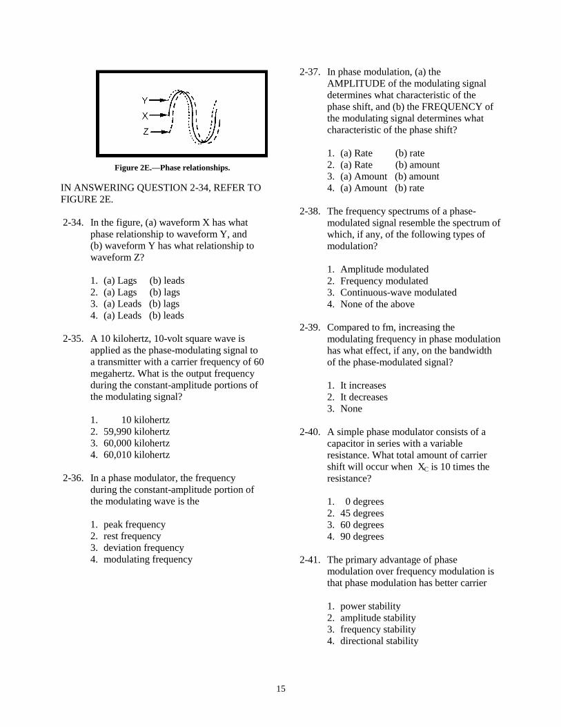
15
Figure 2E.—Phase relationships.
IN ANSWERING QUESTION 2-34, REFER TOFIGURE 2E.
2-34. In the figure, (a) waveform X has whatphase relationship to waveform Y, and(b) waveform Y has what relationship towaveform Z?
1. (a) Lags (b) leads2. (a) Lags (b) lags3. (a) Leads (b) lags4. (a) Leads (b) leads
2-35. A 10 kilohertz, 10-volt square wave isapplied as the phase-modulating signal toa transmitter with a carrier frequency of 60megahertz. What is the output frequencyduring the constant-amplitude portions ofthe modulating signal?
1. 10 kilohertz2. 59,990 kilohertz3. 60,000 kilohertz4. 60,010 kilohertz
2-36. In a phase modulator, the frequencyduring the constant-amplitude portion ofthe modulating wave is the
1. peak frequency2. rest frequency3. deviation frequency4. modulating frequency
2-37. In phase modulation, (a) theAMPLITUDE of the modulating signaldetermines what characteristic of thephase shift, and (b) the FREQUENCY ofthe modulating signal determines whatcharacteristic of the phase shift?
1. (a) Rate (b) rate2. (a) Rate (b) amount3. (a) Amount (b) amount4. (a) Amount (b) rate
2-38. The frequency spectrums of a phase-modulated signal resemble the spectrum ofwhich, if any, of the following types ofmodulation?
1. Amplitude modulated2. Frequency modulated3. Continuous-wave modulated4. None of the above
2-39. Compared to fm, increasing themodulating frequency in phase modulationhas what effect, if any, on the bandwidthof the phase-modulated signal?
1. It increases2. It decreases3. None
2-40. A simple phase modulator consists of acapacitor in series with a variableresistance. What total amount of carriershift will occur when X C is 10 times theresistance?
1. 0 degrees2. 45 degrees3. 60 degrees4. 90 degrees
2-41. The primary advantage of phasemodulation over frequency modulation isthat phase modulation has better carrier
1. power stability2. amplitude stability3. frequency stability4. directional stability
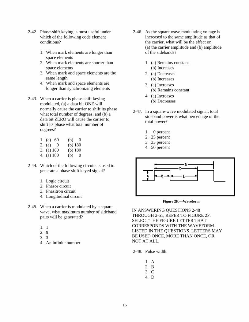
16
2-42. Phase-shift keying is most useful underwhich of the following code elementconditions?
1. When mark elements are longer thanspace elements
2. When mark elements are shorter thanspace elements
3. When mark and space elements are thesame length
4. When mark and space elements arelonger than synchronizing elements
2-43. When a carrier is phase-shift keyingmodulated, (a) a data bit ONE willnormally cause the carrier to shift its phasewhat total number of degrees, and (b) adata bit ZERO will cause the carrier toshift its phase what total number ofdegrees?
1. (a) 60 (b) 02. (a) 0 (b) 1803. (a) 180 (b) 1804. (a) 180 (b) 0
2-44. Which of the following circuits is used togenerate a phase-shift keyed signal?
1. Logic circuit2. Phasor circuit3. Phasitron circuit4. Longitudinal circuit
2-45. When a carrier is modulated by a squarewave, what maximum number of sidebandpairs will be generated?
1. 12. 93. 34. An infinite number
2-46. As the square wave modulating voltage isincreased to the same amplitude as that ofthe carrier, what will be the effect on(a) the carrier amplitude and (b) amplitudeof the sidebands?
1. (a) Remains constant(b) Increases
2. (a) Decreases(b) Increases
3. (a) Increases(b) Remains constant
4. (a) Increases(b) Decreases
2-47. In a square-wave modulated signal, totalsideband power is what percentage of thetotal power?
1. 0 percent2. 25 percent3. 33 percent4. 50 percent
Figure 2F.—Waveform.
IN ANSWERING QUESTIONS 2-48THROUGH 2-51, REFER TO FIGURE 2F.SELECT THE FIGURE LETTER THATCORRESPONDS WITH THE WAVEFORMLISTED IN THE QUESTIONS. LETTERS MAYBE USED ONCE, MORE THAN ONCE, ORNOT AT ALL.
2-48. Pulse width.
1. A2. B3. C4. D
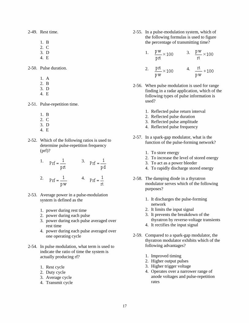
17
2-49. Rest time.
1. B2. C3. D4. E
2-50. Pulse duration.
1. A2. B3. D4. E
2-51. Pulse-repetition time.
1. B2. C3. D4. E
2-52. Which of the following ratios is used todetermine pulse-repetition frequency(prf)?
1. 3.
2. 4.
2-53. Average power in a pulse-modulationsystem is defined as the
1. power during rest time2. power during each pulse3. power during each pulse averaged over
rest time4. power during each pulse averaged over
one operating cycle
2-54. In pulse modulation, what term is used toindicate the ratio of time the system isactually producing rf?
1. Rest cycle2. Duty cycle3. Average cycle4. Transmit cycle
2-55. In a pulse-modulation system, which ofthe following formulas is used to figurethe percentage of transmitting time?
1. 3.
2. 4.
2-56. When pulse modulation is used for rangefinding in a radar application, which of thefollowing types of pulse information isused?
1. Reflected pulse return interval2. Reflected pulse duration3. Reflected pulse amplitude4. Reflected pulse frequency
2-57. In a spark-gap modulator, what is thefunction of the pulse-forming network?
1. To store energy2. To increase the level of stored energy3. To act as a power bleeder4. To rapidly discharge stored energy
2-58. The damping diode in a thyratronmodulator serves which of the followingpurposes?
1. It discharges the pulse-formingnetwork
2. It limits the input signal3. It prevents the breakdown of the
thyratron by reverse-voltage transients4. It rectifies the input signal
2-59. Compared to a spark-gap modulator, thethyratron modulator exhibits which of thefollowing advantages?
1. Improved timing2. Higher output pulses3. Higher trigger voltage4. Operates over a narrower range of
anode voltages and pulse-repetitionrates
18
2-60. To transmit intelligence using pulsemodulation, which of the following pulsecharacteristics may be varied?
1. Pulse duration2. Pulse amplitude3. Pulse-repetition time4. Each of the above
2-61. To accurately reproduce a modulatingsignal in a pulse-modulated system, whatminimum number of samples must betaken per cycle?
1. One2. Two3. Three4. Four
2-62. What is the simplest form of pulsemodulation?
1. Pulse-code modulation2. Pulse-duration modulation3. Pulse-frequency modulation4. Pulse-amplitude modulation
2-63. The same pulse characteristic is varied inwhich of the following types of pulsemodulations?
1. Pam and pdm2. Pdm and pwm3. Pwm and ppm4. Ppm and pam
THIS SPACE LEFT BLANKINTENTIONALLY.
Figure 2G.—Waveform.
IN ANSWERING QUESTION 2-64, REFER TOFIGURE 2G.
2-64. Which of the points shown in thewaveform may be varied in pulse-durationmodulation?
1. A only2. B only3. C only4. A and/or C
2-65. Which, if any, of the following is theprimary disadvantage of pulse-positionmodulation?
1. It depends on transmitter-receiversynchronization
2. It is susceptible to noise interference3. Transmitter power varies4. None of the above
2-66. A pfm transmitter transmits 10,000 pulsesper second without a modulating signalapplied. How, if at all, will a modulatingsignal affect the transmitted pulse rate?
1. It will decrease the transmitted pulserate
2. It will increase the transmitted pulserate
3. Both 1 and 2 above4. It will not affect the transmitted pulse
rate

19
2-67. The process of arbitrarily dividing a waveinto a series of standard values is referredto as
1. arbitration2. quantization3. interposition4. approximation
2-68. A pcm system is capable of transmitting32 standard levels that ate sampled 2.5times per cycle of a 3-kilohertzmodulating signal. What maximumnumber of bits per second are transmitted?
1. 18,7502. 37,5003. 75,0004. 240,000
2-69. Which of the following is a characteristicof a pcm system that makes itadvantageous for use in multiple-relay linksystems?
1. Average power is constant2. Average power decreases with each
relay3. Noise is not cumulative at relay
stations4. Quantization noise decreases with each
relay
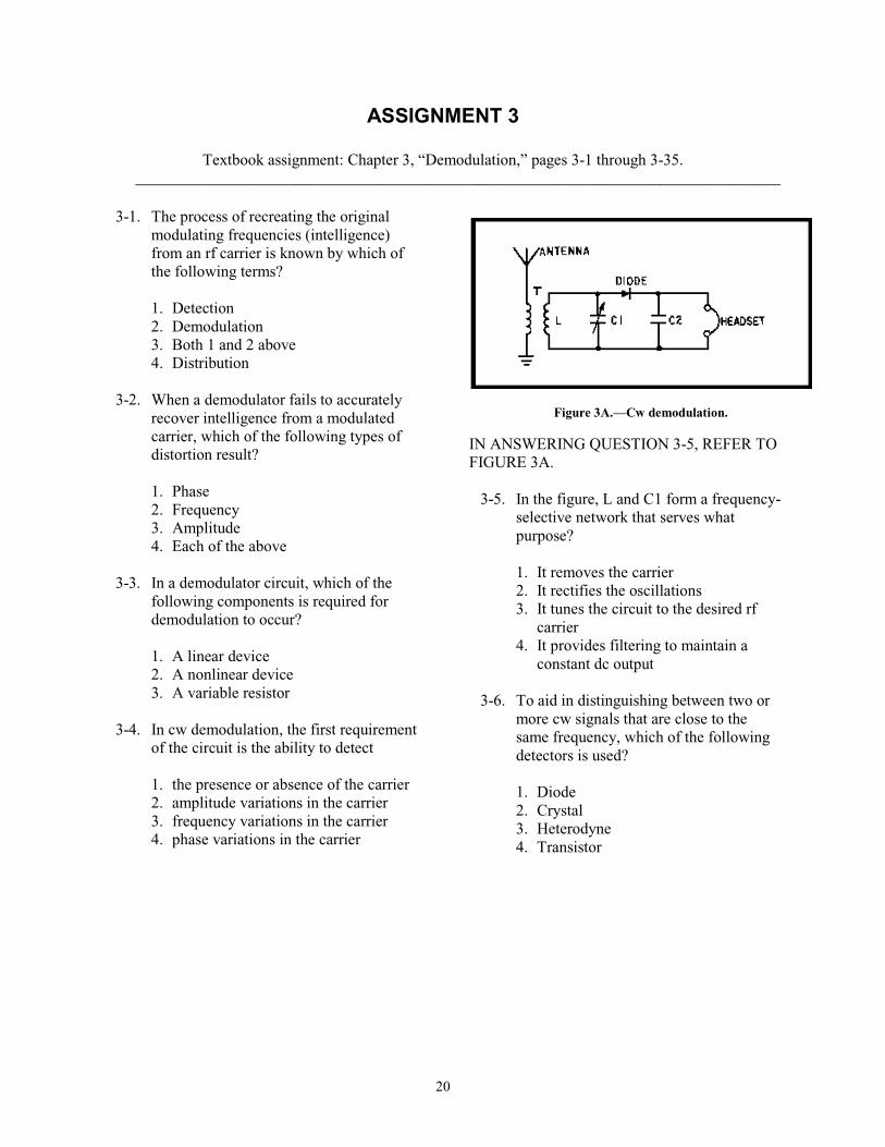
20
ASSIGNMENT 3
Textbook assignment: Chapter 3, “Demodulation,” pages 3-1 through 3-35. _________________________________________________________________________________
3-1. The process of recreating the original modulating frequencies (intelligence) from an rf carrier is known by which of the following terms?
1. Detection 2. Demodulation 3. Both 1 and 2 above 4. Distribution
3-2. When a demodulator fails to accurately recover intelligence from a modulated carrier, which of the following types of distortion result?
1. Phase 2. Frequency 3. Amplitude 4. Each of the above
3-3. In a demodulator circuit, which of the following components is required for demodulation to occur?
1. A linear device 2. A nonlinear device 3. A variable resistor
3-4. In cw demodulation, the first requirement of the circuit is the ability to detect
1. the presence or absence of the carrier 2. amplitude variations in the carrier 3. frequency variations in the carrier 4. phase variations in the carrier
Figure 3A.—Cw demodulation.
IN ANSWERING QUESTION 3-5, REFER TO FIGURE 3A.
3-5. In the figure, L and C1 form a frequency-selective network that serves what purpose?
1. It removes the carrier 2. It rectifies the oscillations 3. It tunes the circuit to the desired rf
carrier 4. It provides filtering to maintain a
constant dc output
3-6. To aid in distinguishing between two or more cw signals that are close to the same frequency, which of the following detectors is used?
1. Diode 2. Crystal 3. Heterodyne 4. Transistor

21
3-7. Assume that two signals are received, one at 500 kHz and the other at 501 kHz. What frequency, in kHz, should be mixed with them to distinguish the 501 kHz signal by producing a 1 kHz output?
1. 499 2. 500 3. 501 4. 502
Figure 3B.—Detector. IN ANSWERING QUESTIONS 3-8 THROUGH 3-11, REFER TO FIGURE 3B.
3-8. The detector circuit in the figure uses the heterodyning principle to detect the incoming signal. What type of detector is it?
1. Hartley 2. Colpitts 3. Armstrong 4. Regenerative
3-9. What component controls the operating frequency of the detector?
1. C1 2. C2 3. L2 4. R1
3-10. What component provides the feedback necessary for oscillations to occur?
1. R1 2. C2 3. C3 4. L2
3-11. Which of the following circuit functions
does Q1 perform?
1. Mixer 2. Detector 3. Oscillator 4. Each of the above
3-12. A circuit that is nonlinear, provides filtering, and is sensitive to the type of modulation applied to it fulfills the requirements of which, if any, of the following circuits?
1. Mixer 2. Modulator 3. Demodulator 4. None of the above
3-13. A detector uses which of the following signals to approximate the original waveform?
1. The sum frequency 2. The carrier frequency 3. The modulation envelope
THIS SPACE LEFT BLANK INTENTIONALLY.
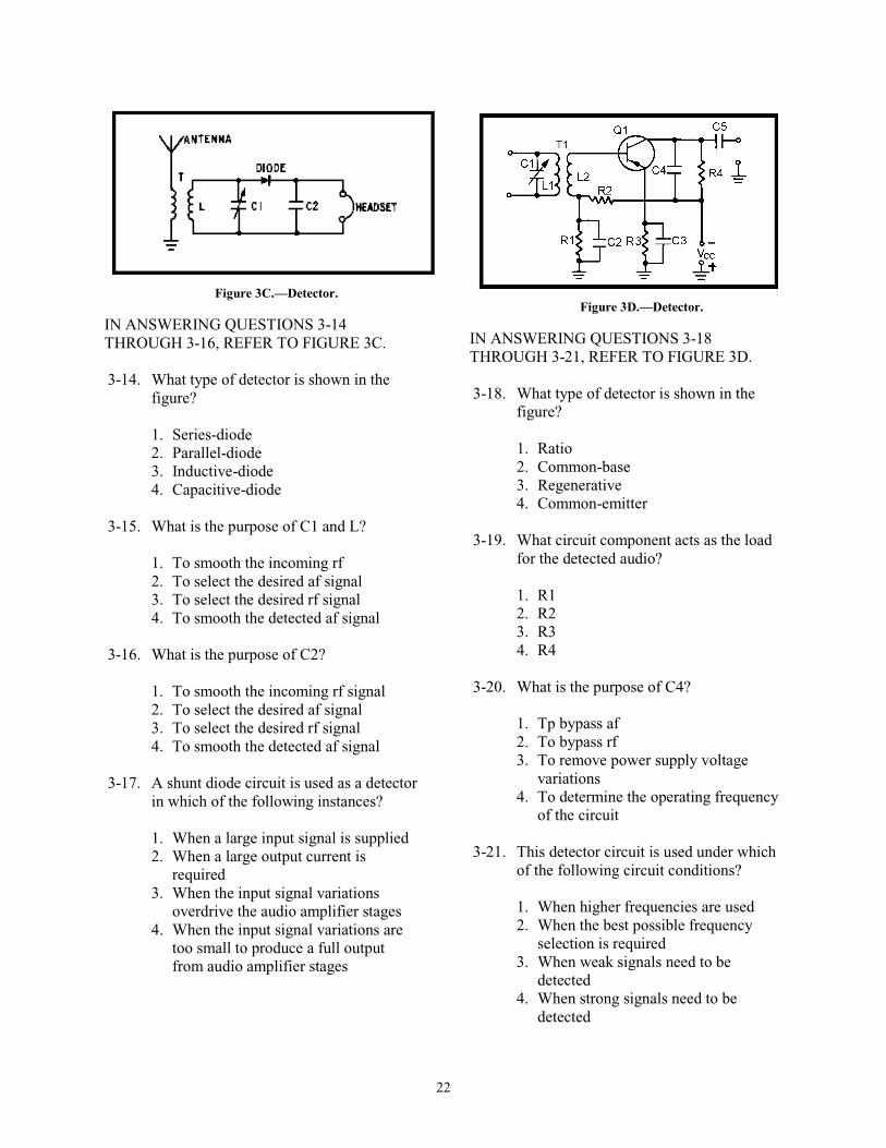
22
Figure 3C.—Detector.
IN ANSWERING QUESTIONS 3-14 THROUGH 3-16, REFER TO FIGURE 3C. 3-14. What type of detector is shown in the
figure?
1. Series-diode 2. Parallel-diode 3. Inductive-diode 4. Capacitive-diode
3-15. What is the purpose of C1 and L?
1. To smooth the incoming rf 2. To select the desired af signal 3. To select the desired rf signal 4. To smooth the detected af signal
3-16. What is the purpose of C2?
1. To smooth the incoming rf signal 2. To select the desired af signal 3. To select the desired rf signal 4. To smooth the detected af signal
3-17. A shunt diode circuit is used as a detector in which of the following instances?
1. When a large input signal is supplied 2. When a large output current is
required 3. When the input signal variations
overdrive the audio amplifier stages 4. When the input signal variations are
too small to produce a full output from audio amplifier stages
Figure 3D.—Detector.
IN ANSWERING QUESTIONS 3-18 THROUGH 3-21, REFER TO FIGURE 3D. 3-18. What type of detector is shown in the
figure?
1. Ratio 2. Common-base 3. Regenerative 4. Common-emitter
3-19. What circuit component acts as the load for the detected audio?
1. R1 2. R2 3. R3 4. R4
3-20. What is the purpose of C4?
1. Tp bypass af 2. To bypass rf 3. To remove power supply voltage
variations 4. To determine the operating frequency
of the circuit
3-21. This detector circuit is used under which of the following circuit conditions?
1. When higher frequencies are used 2. When the best possible frequency
selection is required 3. When weak signals need to be
detected 4. When strong signals need to be
detected
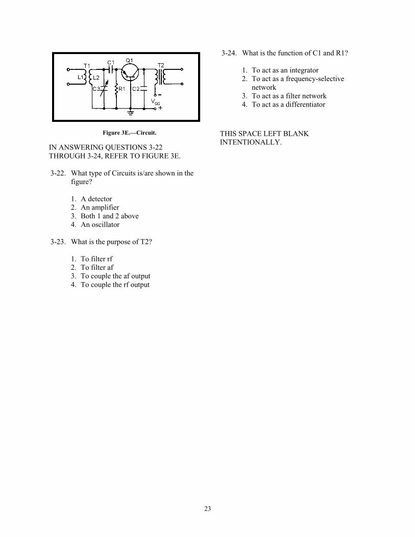
23
Figure 3E.—Circuit.
IN ANSWERING QUESTIONS 3-22 THROUGH 3-24, REFER TO FIGURE 3E. 3-22. What type of Circuits is/are shown in the
figure?
1. A detector 2. An amplifier 3. Both 1 and 2 above 4. An oscillator
3-23. What is the purpose of T2?
1. To filter rf 2. To filter af 3. To couple the af output 4. To couple the rf output
3-24. What is the function of C1 and R1?
1. To act as an integrator 2. To act as a frequency-selective
network 3. To act as a filter network 4. To act as a differentiator
THIS SPACE LEFT BLANK INTENTIONALLY.
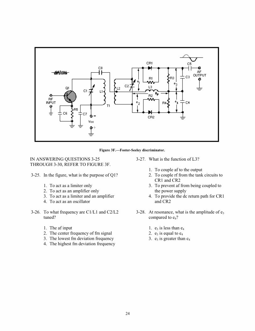
24
Figure 3F.—Foster-Seeley discriminator.
IN ANSWERING QUESTIONS 3-25 THROUGH 3-30, REFER TO FIGURE 3F. 3-25. In the figure, what is the purpose of Q1?
1. To act as a limiter only 2. To act as an amplifier only 3. To act as a limiter and an amplifier 4. To act as an oscillator
3-26. To what frequency are C1/L1 and C2/L2 tuned?
1. The af input 2. The center frequency of fm signal 3. The lowest fm deviation frequency 4. The highest fm deviation frequency
3-27. What is the function of L3?
1. To couple af to the output 2. To couple rf from the tank circuits to
CR1 and CR2 3. To prevent af from being coupled to
the power supply 4. To provide the dc return path for CR1
and CR2
3-28. At resonance, what is the amplitude of e3 compared to e4?
1. e3 is less than e4 2. e3 is equal to e4 3. e3 is greater than e4
25
3-29. When the circuit is operating ABOVE resonance, (a) does inductive reactance increase or decrease, and (b) does capacitive reactance increase or decrease?
1. (a) Increases (b) increases 2. (a) Increases (b) decreases 3. (a) Decreases (b) decreases 4. (a) Decreases (b) increases
3-30. Circuit operation BELOW resonance is represented by which of the following vector diagrams?
1.
2.
3.
THIS SPACE LEFT BLANK INTENTIONALLY.
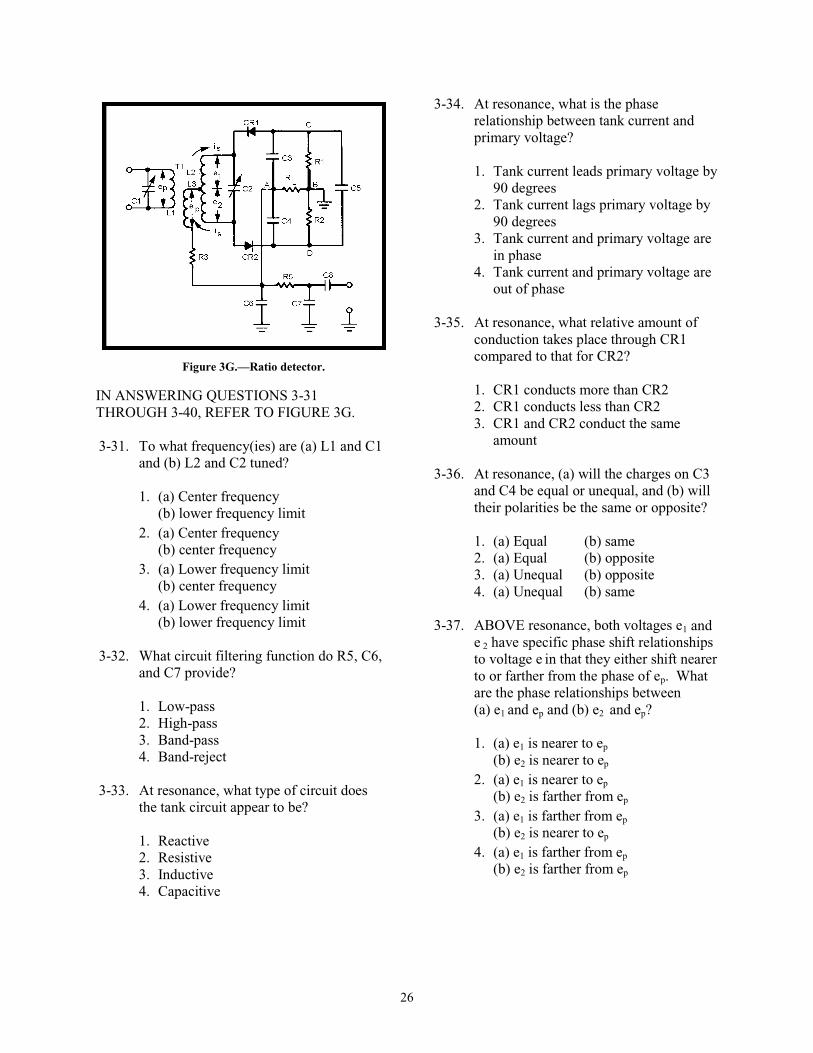
26
Figure 3G.—Ratio detector.
IN ANSWERING QUESTIONS 3-31 THROUGH 3-40, REFER TO FIGURE 3G. 3-31. To what frequency(ies) are (a) L1 and C1
and (b) L2 and C2 tuned?
1. (a) Center frequency (b) lower frequency limit
2. (a) Center frequency (b) center frequency
3. (a) Lower frequency limit (b) center frequency
4. (a) Lower frequency limit (b) lower frequency limit
3-32. What circuit filtering function do R5, C6,
and C7 provide?
1. Low-pass 2. High-pass 3. Band-pass 4. Band-reject
3-33. At resonance, what type of circuit does the tank circuit appear to be?
1. Reactive 2. Resistive 3. Inductive 4. Capacitive
3-34. At resonance, what is the phase relationship between tank current and primary voltage?
1. Tank current leads primary voltage by
90 degrees 2. Tank current lags primary voltage by
90 degrees 3. Tank current and primary voltage are
in phase 4. Tank current and primary voltage are
out of phase
3-35. At resonance, what relative amount of conduction takes place through CR1 compared to that for CR2?
1. CR1 conducts more than CR2 2. CR1 conducts less than CR2 3. CR1 and CR2 conduct the same
amount
3-36. At resonance, (a) will the charges on C3 and C4 be equal or unequal, and (b) will their polarities be the same or opposite? 1. (a) Equal (b) same 2. (a) Equal (b) opposite 3. (a) Unequal (b) opposite 4. (a) Unequal (b) same
3-37. ABOVE resonance, both voltages e1 and
e 2 have specific phase shift relationships to voltage e in that they either shift nearer to or farther from the phase of ep. What are the phase relationships between (a) e1 and ep and (b) e2 and ep?
1. (a) e1 is nearer to ep
(b) e2 is nearer to ep 2. (a) e1 is nearer to ep
(b) e2 is farther from ep 3. (a) e1 is farther from ep
(b) e2 is nearer to ep 4. (a) e1 is farther from ep
(b) e2 is farther from ep
27
3-38. If C3 is charged to 6 volts and C4 is charged to 4 volts, what is the output voltage? 1. 1 volt 2. 2 volts 3. 3 volts 4. 4 volts
3-39. When operating BELOW resonance, what is the relationship of the vector sum of e 1 and ep to the vector sum of e2 and ep?
1. The sum of e1 and ep is larger than the
sum of e2 and ep 2. The sum of e1 and ep is smaller than
the sum of e2 and ep 3. The slam of e1 and ep is equal to the
sum of e2 an ep
3-40. What components help to reduce the effects of amplitude variations at the input of the circuit?
1. R1, R2, and C5 2. R5, C6, and C7 3. R1, R2, C3, and C4 4. L1, L2, L3, and C2
3-41. What is the minimum input voltage, in millivolts, required for a ratio detector?
1. 100 2. 200 3. 300 4. 400
3-42. Which of the following circuit functions is performed by the gated-beam detector?
1. Limiter 2. Detector 3. Amplifier 4. Each of the above
THIS SPACE LEFT BLANK INTENTIONALLY.
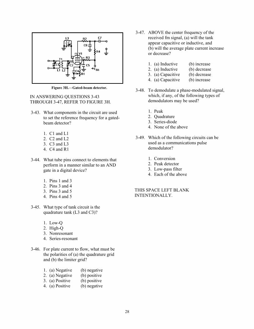
28
Figure 3H.—Gated-beam detector.
IN ANSWERING QUESTIONS 3-43 THROUGH 3-47, REFER TO FIGURE 3H. 3-43. What components in the circuit are used
to set the reference frequency for a gated-beam detector?
1. C1 and L1 2. C2 and L2 3. C3 and L3 4. C4 and R1
3-44. What tube pins connect to elements that perform in a manner similar to an AND gate in a digital device?
1. Pins 1 and 3 2. Pins 3 and 4 3. Pins 3 and 5 4. Pins 4 and 5
3-45. What type of tank circuit is the quadrature tank (L3 and C3)?
1. Low-Q 2. High-Q 3. Nonresonant 4. Series-resonant
3-46. For plate current to flow, what must be the polarities of (a) the quadrature grid and (b) the limiter grid?
1. (a) Negative (b) negative 2. (a) Negative (b) positive 3. (a) Positive (b) positive 4. (a) Positive (b) negative
3-47. ABOVE the center frequency of the received fm signal, (a) will the tank appear capacitive or inductive, and (b) will the average plate current increase or decrease?
1. (a) Inductive (b) increase 2. (a) Inductive (b) decrease 3. (a) Capacitive (b) decrease 4. (a) Capacitive (b) increase
3-48. To demodulate a phase-modulated signal, which, if any, of the following types of demodulators may be used?
1. Peak 2. Quadrature 3. Series-diode 4. None of the above
3-49. Which of the following circuits can be used as a communications pulse demodulator?
1. Conversion 2. Peak detector 3. Low-pass filter 4. Each of the above
THIS SPACE LEFT BLANK INTENTIONALLY.

29
Figure 3I.—Detector.
IN ANSWERING QUESTIONS 3-50 THROUGH 3-52, REFER TO FIGURE 3I. 3-50. To detect pulse-amplitude modulation,
what value must the RC time constant of R1 and C1 in the circuit be?
1. Five times the pulse width 2. Ten times the pulse width 3. Five times the interpulse period 4. Ten times the interpulse period
3-51. Which, if any, of the following functions is the purpose of CR2? 1. To quickly discharge C1 between
received pulses 2. To rectify input pulses 3. To clamp the output to a positive
level 4. None of the above
3-52. What change must be made to the circuit to detect pulse-duration modulation?
1. Remove R1 2. Increase the value of R1 3. Decrease the value of R1 4. Add a resistor in series with CR1
3-53. When a pulse-duration modulated signal is determined by using a low-pass filter, what characteristic of the signal is used?
1. Width 2. Amplitude 3. Frequency 4. Pulse position
3-54. To detect pulse-duration modulation, the
low-pass filter components must be selected so that they pass only the
1. carrier frequency 2. intermediate frequency 3. pulse-repetition frequency 4. desired modulating frequency
3-55. What type(s) of modulation is/are normally detected by first converting it/them to another type of modulation?
1. Ppm only 2. Pfm only 3. Pcm only 4. Ppm, pfm, and pcm
3-56. What type of circuit can be used to convert from ppm to pdm for demodulation?
1. An amplifier 2. A flip-flop 3. An oscillator 4. A transformer
THIS SPACE LEFT BLANK INTENTIONALLY.
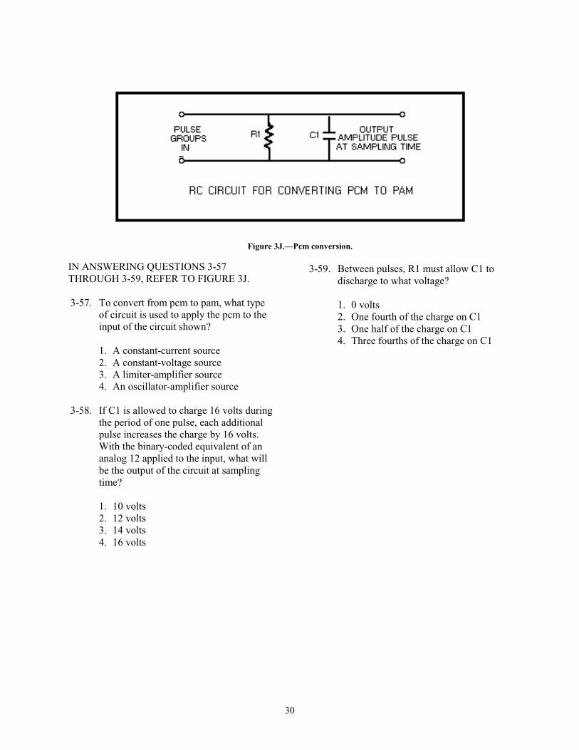
30
Figure 3J.—Pcm conversion.
IN ANSWERING QUESTIONS 3-57 THROUGH 3-59, REFER TO FIGURE 3J. 3-57. To convert from pcm to pam, what type
of circuit is used to apply the pcm to the input of the circuit shown?
1. A constant-current source 2. A constant-voltage source 3. A limiter-amplifier source 4. An oscillator-amplifier source
3-58. If C1 is allowed to charge 16 volts during the period of one pulse, each additional pulse increases the charge by 16 volts. With the binary-coded equivalent of an analog 12 applied to the input, what will be the output of the circuit at sampling time?
1. 10 volts 2. 12 volts 3. 14 volts 4. 16 volts
3-59. Between pulses, R1 must allow C1 to
discharge to what voltage?
1. 0 volts 2. One fourth of the charge on C1 3. One half of the charge on C1 4. Three fourths of the charge on C1