Embed Size (px)
Citation preview
REV. 0
AD1833A
Information furnished by Analog Devices is believed to be accurate andreliable. However, no responsibility is assumed by Analog Devices for itsuse, nor for any infringements of patents or other rights of third parties thatmay result from its use. No license is granted by implication or otherwiseunder any patent or patent rights of Analog Devices. Trademarks andregistered trademarks are the property of their respective companies.
One Technology Way, P.O. Box 9106, Norwood, MA 02062-9106, U.S.A.
Tel: 781/329-4700 www.analog.com
Fax: 781/326-8703 © 2003 Analog Devices, Inc. All rights reserved.
Multichannel,24-Bit, 192 kHz, �-� DAC
FEATURES
5 V Stereo Audio System with 3.3 V Tolerant Digital
Interface
Supports 96 kHz Sample Rates on 6 Channels and
192 kHz on 2 Channels
Supports 16-/20-/24-Bit Word Lengths
Multibit �-� Modulators with
Perfect Differential Linearity Restoration for
Reduced Idle Tones and Noise Floor
Data Directed Scrambling DACs—Least Sensitive to
Jitter
Differential Output for Optimum Performance
DACs Signal-to-Noise and Dynamic Range: 110 dB
–94 dB THD + N—6-Channel Mode
–95 dB THD + N—2-Channel Mode
On-Chip Volume Control per Channel with 1024-Step
Linear Scale
Software Controllable Clickless Mute
Digital De-emphasis Processing
Supports 256 � fS, 512 � fS, and 768 � fS Master
Clock Modes
Power-Down Mode Plus Soft Power-Down Mode
Flexible Serial Data Port with Right-Justified,
Left-Justified, I2S Compatible, and DSP Serial Port Modes
Supports Packed Data Mode and TDM Mode
48-Lead LQFP Plastic Package
APPLICATIONS
DVD Video and Audio Players
Home Theater Systems
Automotive Audio Systems
Set-Top Boxes
Digital Audio Effects Processors
FUNCTIONAL BLOCK DIAGRAM
AGNDDGNDFILTR FILTD
MCLK
CDATA
CLATCH
CCLK
OUTLP1OUTLN1
OUTLP2OUTLN2
OUTLP3OUTLN3
OUTRP3OUTRN3
OUTRP2OUTRN2
OUTRP1OUTRN1
ZERO FLAGSDVD D 1 DVD D 2
AVD D
RESET
SOUTAD1833A
SPIPORT
DATAPORT
L/RCLK
BCLK
SDIN1
SDIN2
SDIN3
INTERPOLATOR DAC
INTERPOLATOR DAC
INTERPOLATOR DAC
INTERPOLATOR DAC
INTERPOLATOR DAC
FILTERENGINE
INTERPOLATOR DAC
GENERAL DESCRIPTIONThe AD1833A is a complete, high performance, single-chip,multichannel, digital audio playback system. It features six audioplayback channels, each comprising a high performance digitalinterpolation filter, a multibit S-D modulator featuring AnalogDevices’ patented technology, and a continuous-time voltage-outanalog DAC section. Other features include an on-chip clicklessattenuator and mute capability for each channel, programmedthrough an SPI compatible serial control port.
The AD1833A is fully compatible with all known DVD formats,accommodating word lengths of up to 24 bits at sample rates of48 kHz and 96 kHz on all six channels while supporting a 192 kHzsample rate on two channels. It also provides the Redbook stan-dard 50 ms/15 ms digital de-emphasis filters at sample rates of32 kHz, 44.1 kHz, and 48 kHz.
The AD1833A has a very flexible serial data input port thatallows glueless interconnection to a variety of ADCs, DSP chips,AES/EBU receivers, and sample rate converters. It can be con-figured in right-justified, left-justified, I2S, or DSP serial portcompatible modes. The AD1833A accepts serial audio data in MSBfirst, twos complement format. The AD1833A can be operatedfrom a single 5 V power supply; it also features a separate supplypin for its digital interface that allows it to be interfaced to devicesusing 3.3 V power supplies.
The AD1833A is fabricated on a single monolithic integratedcircuit and is housed in a 48-lead LQFP package for operationfrom –40∞C to +85∞C.

REV. 0–2–
AD1833A–SPECIFICATIONS
Parameter Min Typ Max Unit Test Conditions
ANALOG PERFORMANCEDIGITAL-TO-ANALOG CONVERTERS
Dynamic Range (20 Hz to 20 kHz, –60 dBFS Input)with A-Weighted FilterAD1833AA 106.5 110.0 dBAD1833AA 110.5 dB fS = 96 kHzAD1833AC 107.0 dB
Total Harmonic Distortion + Noise –95 –89 dB Two channels active–94 dB Six channels active–95 dB 96 kHz, two channels active–94 dB 96 kHz, six channels active
SNR 110 dBInterchannel Isolation 108 dBDC Accuracy
Gain Error ± 3 %Interchannel Gain Mismatch 0.2 %Gain Drift 80 ppm/∞C
Interchannel Crosstalk (EIAJ Method) –120 dBInterchannel Phase Deviation ± 0.1 DegreesVolume Control Step Size (1023 Linear Steps) 0.098 %Volume Control Range (Max Attenuation) +63.5 (0.098) dB (%)Mute Attenuation –63.5 (0.098) dB (%)De-emphasis Gain Error ± 0.1 dBFull-Scale Output Voltage at Each Pin (Single-Ended) 1 (2.8) V rms (V p-p)Output Resistance Measured Differentially 150 WCommon-Mode Output Volts 2.2 V
DAC INTERPOLATION FILTER—8� Mode (48 kHz)Pass Band 21.768 kHzPass-Band Ripple ± 0.01 dBStop Band 24 kHzStop-Band Attenuation 70 dBGroup Delay 510 ms
DAC INTERPOLATION FILTER—4� Mode (96 kHz)Pass Band 37.7 kHzPass-Band Ripple ± 0.03 dBStop Band 55.034 kHzStop-Band Attenuation 70 dBGroup Delay 160 ms
DAC INTERPOLATION FILTER—2� Mode (192 kHz)Pass Band 89.954 kHzPass-Band Ripple ± 1 dBStop Band 104.85 kHzStop-Band Attenuation 70 dBGroup Delay 140 ms
TEST CONDITIONS, UNLESS OTHERWISE NOTED*
Supply Voltages (AVDD, DVDDX) 5 VAmbient Temperature 25∞CInput Clock 12.288 MHz, (8� Mode)Input Signal Nominally 1 kHz, 0 dBFS
(Full-Scale)Input Sample Rate 48 kHzMeasurement Bandwidth 20 Hz to 20 kHzWord Width 24 BitsLoad Capacitance 100 pFLoad Impedance 10 kW*Performance is identical for all channels (except for the Interchannel GainMismatch and Interchannel Phase Deviation specifications).
REV. 0 –3–
AD1833AParameter Min Typ Max Unit Test Conditions
DIGITAL I/OInput Voltage HI 2.4 VInput Voltage LO 0.8 VOutput Voltage HI DVDD2 – 0.4 VOutput Voltage LO 0.4 V
POWER SUPPLIESSupply Voltage (AVDD and DVDD1) 4.5 5 5.5 VSupply Voltage (DVDD2) 3.3 DVDD1 VSupply Current IANALOG 38.5 42 mASupply Current IDIGITAL 42 48 mA Active
2 mA Power-DownPower Supply Rejection Ratio
1 kHz 300 mV p-p Signal at Analog Supply Pins –60 dB20 kHz 300 mV p-p Signal at Analog Supply Pins –50 dB
Specifications subject to change without notice.
DIGITAL TIMINGParameter Min Max Unit Comments
MASTER CLOCK AND RESETtML MCLK LO (All Modes)* 15 ns 24 MHz clock, clock doubler bypassedtMH MCLK HI (All Modes)* 15 ns 24 MHz clock, clock doubler bypassedtPDR PD/RST LO 20 ns
SPI PORTtCCH CCLK HI Pulsewidth 20 nstCCL CCLK LO Pulsewidth 20 nstCCP CCLK Period 80 nstCDS CDATA Setup Time 10 ns To CCLK risingtCDH CDATA Hold Time 10 ns From CCLK risingtCLS CLATCH Setup 10 ns To CCLK risingtCLH CLATCH Hold 10 ns From CCLK rising
DAC SERIAL PORTtDBH BCLK HI 15 nstDBL BCLK LO 15 nstDLS L/RCLK Setup 10 ns To BCLK risingtDLH L/RCLK Hold 10 ns From BCLK risingtDDS SDATA Setup 10 ns To BCLK risingtDDH SDATA Hold 15 ns From BCLK rising
TDM MODE MASTERtTMBD BCLKTDM Delay 20 ns From MCLK risingtTMFSD FSTDM Delay 10 ns From BCLKTDM risingtTMDDS SDIN1 Setup 15 ns To BCLKTDM fallingtTMDDH SDIN1 Hold 15 ns From BCLKTDM falling
TDM MODE SLAVEfTSB BCLKTDM Frequency 256 � fS
tTSBCH BCLKTDM High 20 nstTSBCL BCLKTDM Low 20 nstTSFS FSTDM Setup 10 ns To BCLKTDM fallingtTSFH FSTDM Hold 10 ns From BCLKTDM fallingtTSDDS SDIN1 Setup 15 ns To BCLKTDM fallingtTSDDH SDIN1 Hold 15 ns From BCLKTDM falling
AUXILIARY INTERFACEtAXLRD L/RCLK Delay 10 ns From BCLK fallingtAXDD Data Delay 10 ns From BCLK fallingtAXBD AUXBCLK Delay 20 ns From MCLK rising
*MCLK symmetry must be better than 60:40 or 40:60.
Specifications subject to change without notice.
(Guaranteed over –40�C to +85�C, AVDD = DVDD = 5 V � 10%)

REV. 0–4–
AD1833A
MCLK
tMH
PD/RST
tML
tPDR
Figure 1. MCLK and RESET Timing
CLATCH
CCLK
CIN D0D15 D14 D8
tCCH tCCL
D9
tCDS tCDH
tCLS tCLH
tCCP
Figure 2. SPI Port Timing
BCLK
L/RCLK
SDATALEFT-JUSTIFIED
MODE
SDATARIGHT-JUSTIFIED
MODELSB
SDATAI2S MODE
MSB MSB-1
MSB
MSB
tDBH
tDBL
tDLS
tDDS
tDDH
tDDS
tDLH
tDDH
tDDS tDDS
tDDH tDDH
Figure 3. Serial Port Timing
MSB
tTMBD
tTMFSD
tTMDDS tTMDDH
MCLK
BCLKTDM
FSTDM
SDIN1
tTSBCL tTSBCH
tTSDDHtTSDDS
tTSFS tTSFH
Figure 4. TDM Master and Slave Mode Timing

REV. 0
AD1833A
–5–
ABSOLUTE MAXIMUM RATINGS*(TA = 25∞C, unless otherwise noted.)
AVDD, DVDDX to AGND, DGND . . . . . . . . –0.3 V to +6.5 VAGND to DGND . . . . . . . . . . . . . . . . . . . . –0.3 V to +0.3 VDigital I/O Voltage to DGND . . . . . –0.3 V to DVDD2 + 0.3 VAnalog I/O Voltage to AGND . . . . . . –0.3 V to AVDD + 0.3 VOperating Temperature Range
Industrial (A Version) . . . . . . . . . . . . . . . –40∞C to +85∞CStorage Temperature Range . . . . . . . . . . . . –65∞C to +150∞CMaximum Junction Temperature . . . . . . . . . . . . . . . . 150∞C
LQFP, qJA Thermal Impedance . . . . . . . . . . . . . . . . . 91∞C/WLead Temperature, Soldering
Vapor Phase (60 sec) . . . . . . . . . . . . . . . . . . . . . . . . 215∞CInfrared (15 sec) . . . . . . . . . . . . . . . . . . . . . . . . . . . . 220∞C
*Stresses above those listed under Absolute Maximum Ratings may cause perma-nent damage to the device. This is a stress rating only; functional operation of thedevice at these or any other conditions above those listed in the operationalsections of this specification is not implied. Exposure to absolute maximum ratingconditions for extended periods may affect device reliability. Only one absolutemaximum rating may be applied at any one time.
MSB
MCLK
AUXBCLK
AUXL/RCLK
AUX DATA
tAXDD
tAXLRD
tAXBD
Figure 5. Auxiliary Interface Timing
ORDERING GUIDE
Model Temperature Range Package Description Package Option
AD1833AAST –40∞C to +85∞C Low Profile Quad Flat Package ST-48AD1833ACST –40∞C to +85∞C Low Profile Quad Flat Package ST-48EVAL-AD1833AEB Evaluation BoardAD1833AAST-REEL –40∞C to +85∞C Low Profile Quad Flat Package ST-48AD1833ACST-REEL –40∞C to +85∞C Low Profile Quad Flat Package ST-48
CAUTIONESD (electrostatic discharge) sensitive device. Electrostatic charges as high as 4000 V readily accumulateon the human body and test equipment and can discharge without detection. Although the AD1833Afeatures proprietary ESD protection circuitry, permanent damage may occur on devices subjected tohigh energy electrostatic discharges. Therefore, proper ESD precautions are recommended to avoidperformance degradation or loss of functionality.

REV. 0
AD1833A
–6–
PIN CONFIGURATION
36
35
34
33
32
31
30
29
28
27
26
25
13 14 15 16 17 18 19 20 21 22 23 24
1
2
3
4
5
6
7
8
9
10
11
12
48 47 46 45 44 39 38 3743 42 41 40
PIN 1IDENTIFIER
TOP VIEW(Not to Scale)
OUTRP1
OUTRN1
AVDDAVDDAGND
AGND
AGND
OUTLP1
OUTLN1
AVDDAVDD
AGND
AGND
AGND
DGND
DVDD1ZEROA
ZERO3R
DGND
DVDD2
RESETZERO1L
AD1833A
ZERO3L ZERO1RO
UT
LN
2
OU
TL
P2
OU
TL
N3
OU
TL
P3
AV
DD
FIL
TD
FIL
TR
AG
ND
OU
TR
P3
OU
TR
N3
OU
TR
P2
OU
TR
N2
ZE
RO
2RC
LA
TC
H
CD
AT
A
CC
LK
L/R
CL
K
BC
LK
MC
LK
SD
IN1
SD
IN2
SD
IN3
SO
UT
ZE
RO
2L
PIN FUNCTION DESCRIPTIONS
Pin No. Mnemonic IN/OUT Description
1 OUTLP1 O DAC 1 Left Channel Positive Output.2 OUTLN1 O DAC 1 Left Channel Negative Output.3, 4, 33, 34, 44 AVDD Analog Supply.5, 6, 7, 30, 31, 32, 41 AGND Analog Ground.8, 29 DGND Digital Ground.9 DVDD1 Digital Supply to Core Logic.10 ZEROA O Flag to Indicate Zero Input on All Channels.11 ZERO3R O Flag to Indicate Zero Input on Channel 3 Right.12 ZERO3L O Flag to Indicate Zero Input on Channel 3 Left.13 ZERO2R O Flag to Indicate Zero Input on Channel 2 Right.14 CLATCH I Latch Input for Control Data (SPI Port).15 CDATA I Serial Control Data Input (SPI Port).16 CCLK I Clock Input for Control Data (SPI Port).17 L/RCLK I/O Left/Right Clock for DAC Data Input; FSTDM Input in TDM Slave Mode;
FSTDM Output in TDM Master Mode.18 BCLK I/O Bit Clock for DAC Data Input; BCLKTDM Input in TDM Slave Mode; BCLKTDM
Output in TDM Master Mode.19 MCLK I Master Clock Input.20 SDIN1 I Data Input for Channel 1 Left/Right (Data Stream Input in TDM and Packed Modes).21 SDIN2 I/O Data Input for Channel 2 Left/Right (L/RCLK Output to Auxiliary DAC in
TDM Mode).22 SDIN3 I/O Data Input for Channel 3 Left/Right (BCLK Output to Auxiliary DAC in TDM Mode).23 SOUT O Auxiliary I2S Output (Available in TDM Mode).24 ZERO2L O Flag to Indicate Zero Input on Channel 2 Left.25 ZERO1R O Flag to Indicate Zero Input on Channel 1 Right.26 ZERO1L O Flag to Indicate Zero Input on Channel 1 Left.27 RESET I Power-Down and Reset Control.28 DVDD2 Power Supply to Output Interface Logic.35 OUTRN1 O DAC 1 Right Channel Negative Output.36 OUTRP1 O DAC 1 Right Channel Positive Output.37 OUTRN2 O DAC 2 Right Channel Negative Output.38 OUTRP2 O DAC 2 Right Channel Positive Output.39 OUTRN3 O DAC 3 Right Channel Negative Output.
REV. 0
AD1833A
–7–
DEFINITION OF TERMSDynamic RangeThe ratio of a full-scale input signal to the integrated input noise inthe pass band (20 Hz to 20 kHz), expressed in decibels. Dynamicrange is measured with a –60 dB input signal and is equal to(S/[THD + N]) +60 dB. Note that spurious harmonics are belowthe noise with a –60 dB input, so the noise level establishes thedynamic range. The dynamic range is specified with and withoutan A-Weight filter applied.
Signal to (Total Harmonic Distortion + Noise)[S/(THD + N)]The ratio of the root-mean-square (rms) value of the fundamentalinput signal to the rms sum of all other spectral components inthe pass band, expressed in decibels.
Pass BandThe region of the frequency spectrum unaffected by the attenuationof the digital decimator’s filter.
Pass-Band RippleThe peak-to-peak variation in amplitude response from equal-amplitude input signal frequencies within the pass band, expressedin decibels.
Stop BandThe region of the frequency spectrum attenuated by the digitaldecimator’s filter to the degree specified by stop-band attenuation.
Gain ErrorWith a near full-scale input, the ratio of actual output to expectedoutput, expressed as a percentage.
Interchannel Gain MismatchWith identical near full-scale inputs, the ratio of outputs of thetwo stereo channels, expressed in decibels.
Gain DriftChange in response to a nearly full-scale input with a change intemperature, expressed as parts-per-million (ppm/∞C).
Crosstalk (EIAJ Method)Ratio of response on one channel with a grounded input to afull-scale 1 kHz sine wave input on the other channel, expressedin decibels.
Power Supply RejectionWith no analog input, signal present at the output when a300 mV p-p signal is applied to the power supply pins, expressedin decibels of full scale.
Group DelayIntuitively, the time interval required for an input pulse to appearat the converter’s output, expressed in ms. More precisely, thederivative of radian phase with respect to the radian frequency ata given frequency.
Group Delay VariationThe difference in group delays at different input frequencies.Specified as the difference between the largest and the smallestgroup delays in the pass band, expressed in ms.
PIN FUNCTION DESCRIPTIONS (continued)
Pin No. Mnemonic IN/OUT Description
40 OUTRP3 O DAC 3 Right Channel Positive Output.42 FILTR Reference/Filter Capacitor Connection. Recommend 0.1 mF/10 mF decouple to
analog ground.43 FILTD Filter Capacitor Connection. Recommend 0.1 mF/10 mF decouple to analog ground.45 OUTLP3 O DAC 3 Left Channel Positive Output.46 OUTLN3 O DAC 3 Left Channel Negative Output.47 OUTLP2 O DAC 2 Left Channel Positive Output.48 OUTLN2 O DAC 2 Left Channel Negative Output.
REV. 0
AD1833A
–8–
0.010
0 0.2 0.4 0.6 0.8 1.0 1.2 1.4 1.6 1.8 2.0
0.008
0.006
0.004
0.002
0
–0.002
–0.004
–0.006
–0.008
–0.010
dB
Hz �104
TPC 1. Pass-Band Response, 8� Mode
10
2.00 2.05 2.10 2.15 2.20 2.25 2.30 2.35 2.40 2.45 2.50
0
–10
–20
–30
dB
Hz �104
–40
–50
–60
–70
–80
–90
–100
TPC 2. Transition Band Response, 8� Mode
0 0.5 1.5 2.0 2.5 3.0
0
–20
–40
–60
–80
–100
–120
–140
–160
dB
Hz �105
1.0
TPC 3. Complete Response, 8� Mode
–Typical Performance Characteristics0.10
0 0.5 1.0 1.5 2.0 2.5 3.0 3.5
0.08
0.06
0.04
0.02
0
–0.02
–0.04
–0.06
–0.08
–0.10
dB
Hz �104
TPC 4. Pass-Band Response, 4� Mode
0.5
0 0.5 1.0 1.5 2.0 2.5 3.0 3.5 4.0
0.4
0.3
0.2
0.1
0
–0.1
–0.2
–0.3
–0.4
–0.5
dB
Hz �104
TPC 5. 40 kHz Pass-Band Response, 4� Mode
10
4.0 4.2 4.4 4.6 4.8 5.0 5.2 5.4 5.6 5.8 6.0
0
–10
–20
–30
dB
Hz �104
–40
–50
–60
–70
–80
–90
–100
TPC 6. Transition Band Response, 4� Mode
REV. 0
AD1833A
–9–
0 0.5 1.5 2.0
0
–20
–40
–60
–80
–100
–120
–140
–160
dB
Hz �105
1.0 2.5 3.0
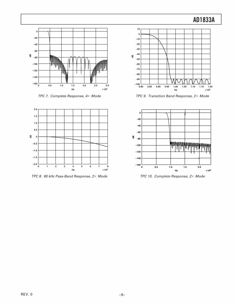
TPC 7. Complete Response, 4� Mode
2.0
0 1 2 3 4 5 6 7 8
1.5
0.5
0
–0.5
–1.0
–1.5
–2.0
dB
Hz �104
1.0
TPC 8. 80 kHz Pass-Band Response, 2� Mode
10
0.80 0.85 0.90 0.95 1.00 1.05 1.10 1.15 1.20
0
–10
–20
–30
dB
Hz �105
–40
–50
–60
–70
–80
–90
–100
TPC 9. Transition Band Response, 2� Mode
0 0.5 1.5 2.0
0
–20
–40
–60
–80
–100
–120
–140
–160
dB
Hz �105
1.0
TPC 10. Complete Response, 2� Mode
REV. 0
AD1833A
–10–
FUNCTIONAL DESCRIPTIONDevice ArchitectureThe AD1833A is a six-channel audio DAC featuring multibitsigma-delta (S-D) technology. The AD1833A features three stereoconverters (providing six channels); each stereo channel is con-trolled by a common bit-clock (BCLK) and synchronizationsignal (L/RCLK).
General OverviewThe AD1833A is designed to run with an internal MCLK(IMCLK) of 24.576 MHz and a modulator rate of 6.144 MHz(i.e., IMCLK/4). From this IMCLK frequency, sample rates of48 kHz and 96 kHz can be achieved on six channels or 192 kHzcan be achieved on two channels. The internal clock should neverbe run at a higher frequency but may be reduced to achievelower sampling rates, i.e., for a sample rate of 44.1 kHz, the appro-priate internal MCLK is 22.5792 MHz. The modulator rate scalesin proportion with the MCLK scaling.
InterpolatorThe interpolator consists of as many as three stages of samplerate doubling and half-band filtering followed by a 16-samplezero order hold (ZOH). The sample rate doubling is achievedby zero stuffing the input samples, and a digital half-band filteris used to remove any images above the band of interest and tobring the zero samples to their correct values.
The interpolator output must always be at a rate of IMCLK/64.Depending on the interpolation rates selected, one, two, or allthree stages of doubling may be switched in. This allows forthree different sample rate inputs for any given IMCLK. For anIMCLK of 24.576 MHz, all three doubling stages are used witha 48 kHz input sample rate; with a 96 kHz input sample rate, onlytwo doubling stages are used; and with a 192 kHz input sample
rate, only one doubling stage is used. In each case, the inputsample frequency is increased to 384 kHz (IMCLK/64). TheZOH holds the interpolator samples for upsampling by themodulator. This is done at a rate 16 times the interpolatoroutput sample rate.
ModulatorThe modulator is a 6-bit, second order implementation and usesdata scrambling techniques to achieve perfect linearity. The modu-lator samples the output of the interpolator stage(s) at a rate of(IMCLK/4).
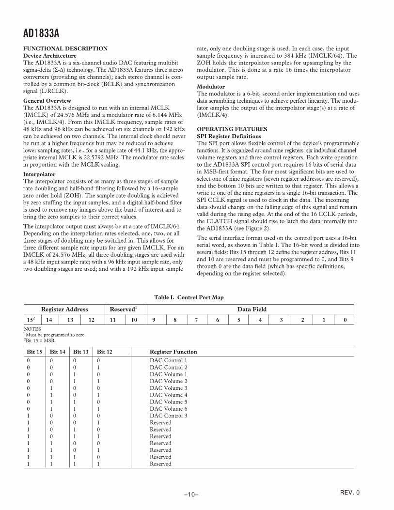
OPERATING FEATURESSPI Register DefinitionsThe SPI port allows flexible control of the device’s programmablefunctions. It is organized around nine registers: six individual channelvolume registers and three control registers. Each write operationto the AD1833A SPI control port requires 16 bits of serial datain MSB-first format. The four most significant bits are used toselect one of nine registers (seven register addresses are reserved),and the bottom 10 bits are written to that register. This allows awrite to one of the nine registers in a single 16-bit transaction. TheSPI CCLK signal is used to clock in the data. The incomingdata should change on the falling edge of this signal and remainvalid during the rising edge. At the end of the 16 CCLK periods,the CLATCH signal should rise to latch the data internally intothe AD1833A (see Figure 2).
The serial interface format used on the control port uses a 16-bitserial word, as shown in Table I. The 16-bit word is divided intoseveral fields: Bits 15 through 12 define the register address, Bits 11and 10 are reserved and must be programmed to 0, and Bits 9through 0 are the data field (which has specific definitions,depending on the register selected).
Table I. Control Port Map
Register Address Reserved1 Data Field
152 14 13 12 11 10 9 8 7 6 5 4 3 2 1 0NOTES1Must be programmed to zero.2Bit 15 = MSB.
Bit 15 Bit 14 Bit 13 Bit 12 Register Function
0 0 0 0 DAC Control 10 0 0 1 DAC Control 20 0 1 0 DAC Volume 10 0 1 1 DAC Volume 20 1 0 0 DAC Volume 30 1 0 1 DAC Volume 40 1 1 0 DAC Volume 50 1 1 1 DAC Volume 61 0 0 0 DAC Control 31 0 0 1 Reserved1 0 1 0 Reserved1 0 1 1 Reserved1 1 0 0 Reserved1 1 0 1 Reserved1 1 1 0 Reserved1 1 1 1 Reserved
REV. 0
AD1833A
–11–
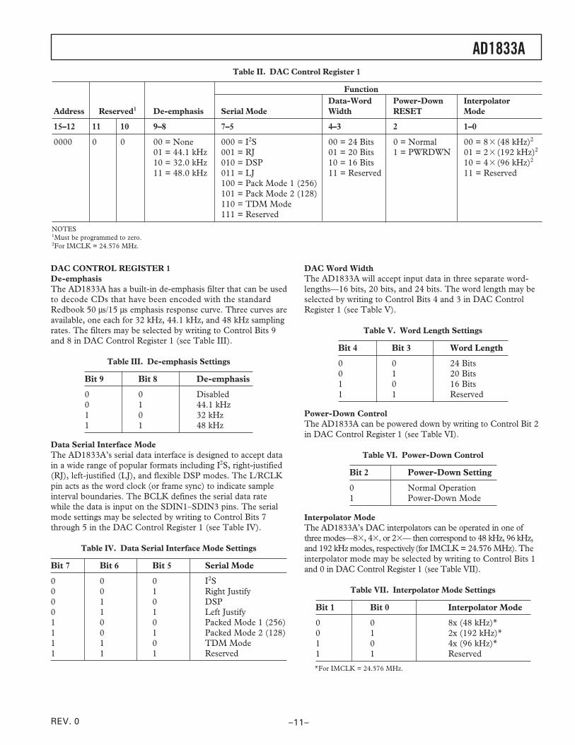
DAC Word WidthThe AD1833A will accept input data in three separate word-lengths—16 bits, 20 bits, and 24 bits. The word length may beselected by writing to Control Bits 4 and 3 in DAC ControlRegister 1 (see Table V).
Table V. Word Length Settings
Bit 4 Bit 3 Word Length
0 0 24 Bits0 1 20 Bits1 0 16 Bits1 1 Reserved
Power-Down ControlThe AD1833A can be powered down by writing to Control Bit 2in DAC Control Register 1 (see Table VI).
Table VI. Power-Down Control
Bit 2 Power-Down Setting
0 Normal Operation1 Power-Down Mode
Interpolator ModeThe AD1833A’s DAC interpolators can be operated in one ofthree modes—8�, 4�, or 2�— then correspond to 48 kHz, 96 kHz,and 192 kHz modes, respectively (for IMCLK = 24.576 MHz). Theinterpolator mode may be selected by writing to Control Bits 1and 0 in DAC Control Register 1 (see Table VII).
Table VII. Interpolator Mode Settings
Bit 1 Bit 0 Interpolator Mode
0 0 8x (48 kHz)*0 1 2x (192 kHz)*1 0 4x (96 kHz)*1 1 Reserved
*For IMCLK = 24.576 MHz.
DAC CONTROL REGISTER 1De-emphasisThe AD1833A has a built-in de-emphasis filter that can be usedto decode CDs that have been encoded with the standardRedbook 50 ms/15 ms emphasis response curve. Three curves areavailable, one each for 32 kHz, 44.1 kHz, and 48 kHz samplingrates. The filters may be selected by writing to Control Bits 9and 8 in DAC Control Register 1 (see Table III).
Table III. De-emphasis Settings
Bit 9 Bit 8 De-emphasis
0 0 Disabled0 1 44.1 kHz1 0 32 kHz1 1 48 kHz
Data Serial Interface ModeThe AD1833A’s serial data interface is designed to accept datain a wide range of popular formats including I2S, right-justified(RJ), left-justified (LJ), and flexible DSP modes. The L/RCLKpin acts as the word clock (or frame sync) to indicate sampleinterval boundaries. The BCLK defines the serial data ratewhile the data is input on the SDIN1–SDIN3 pins. The serialmode settings may be selected by writing to Control Bits 7through 5 in the DAC Control Register 1 (see Table IV).
Table IV. Data Serial Interface Mode Settings
Bit 7 Bit 6 Bit 5 Serial Mode
0 0 0 I2S0 0 1 Right Justify0 1 0 DSP0 1 1 Left Justify1 0 0 Packed Mode 1 (256)1 0 1 Packed Mode 2 (128)1 1 0 TDM Mode1 1 1 Reserved
Table II. DAC Control Register 1
FunctionData-Word Power-Down Interpolator
Address Reserved1 De-emphasis Serial Mode Width RESET Mode
15–12 11 10 9–8 7–5 4–3 2 1–0
0000 0 0 00 = None 000 = I2S 00 = 24 Bits 0 = Normal 00 = 8� (48 kHz)2
01 = 44.1 kHz 001 = RJ 01 = 20 Bits 1 = PWRDWN 01 = 2� (192 kHz)2
10 = 32.0 kHz 010 = DSP 10 = 16 Bits 10 = 4� (96 kHz)2
11 = 48.0 kHz 011 = LJ 11 = Reserved 11 = Reserved100 = Pack Mode 1 (256)101 = Pack Mode 2 (128)110 = TDM Mode111 = Reserved
NOTES1Must be programmed to zero.2For IMCLK = 24.576 MHz.
REV. 0
AD1833A
–12–
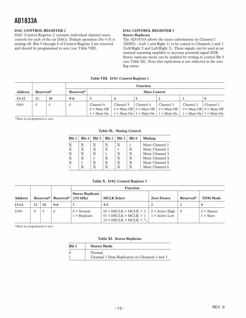
Table X. DAC Control Register 3
Function
Stereo ReplicateAddress Reserved* Reserved* (192 kHz) MCLK Select Zero Detect Reserved* TDM Mode
15–12 11 10 9–6 5 4–3 2 1 0
1000 0 0 0 0 = Normal 00 = IMCLK = MCLK � 2 0 = Active High 0 0 = Master1 = Replicate 01 = IMCLK = MCLK � 1 1 = Active Low 1 = Slave
10 = IMCLK = MCLK � 2/3
*Must be programmed to zero.
DAC CONTROL REGISTER 2DAC Control Register 2 contains individual channel mutecontrols for each of the six DACs. Default operation (bit = 0) ismuting off. Bits 9 through 6 of Control Register 2 are reservedand should be programmed to zero (see Table VIII).
DAC CONTROL REGISTER 3Stereo ReplicateThe AD1833A allows the stereo information on Channel 1(SDIN1—Left 1 and Right 1) to be copied to Channels 2 and 3(Left/Right 2 and Left/Right 3). These signals can be used in anexternal summing amplifier to increase potential signal SNR.Stereo replicate mode can be enabled by writing to control Bit 5(see Table XI). Note that replication is not reflected in the zeroflag status.
Table XI. Stereo Replicate
Bit 5 Stereo Mode
0 Normal1 Channel 1 Data Replicated on Channels 2 and 3
Table VIII. DAC Control Register 2
Function
Address Reserved* Reserved* Mute Control
15–12 11 10 9–6 5 4 3 2 1 0
0001 0 0 0 Channel 6 Channel 5 Channel 4 Channel 3 Channel 2 Channel 10 = Mute Off 0 = Mute Off 0 = Mute Off 0 = Mute Off 0 = Mute Off 0 = Mute Off1 = Mute On 1 = Mute On 1 = Mute On 1 = Mute On 1 = Mute On 1 = Mute On
*Must be programmed to zero.
Table IX. Muting Control
Bit 5 Bit 4 Bit 3 Bit 2 Bit 1 Bit 0 Muting
X X X X X 1 Mute Channel 1X X X X 1 X Mute Channel 2X X X 1 X X Mute Channel 3X X 1 X X X Mute Channel 4X 1 X X X X Mute Channel 51 X X X X X Mute Channel 6

REV. 0
AD1833A
–13–
MCLK SelectThe AD1833A allows the matching of available external MCLKfrequencies to the required internal MCLK rate. The MCLKmodification factor can be selected from 2, 1, or 2/3 by writing toBit 4 and Bit 3 of Control Register 3. Internally, the AD1833Arequires an MCLK of 24.576 MHz for sample rates of 48 kHz,96 kHz, and 192 kHz. In the case of 48 kHz data with anMCLK of 256 � fS, a clock doubler is used, whereas with anMCLK of 768 � fS, a divide-by-3 block (�3) is first implementedfollowed by a clock doubler. With an MCLK of 512 � fS, theMCLK is passed through unmodified (see Table XII).
Table XII. MCLK Settings
Bit 4 Bit 3 Modification Factor
0 0 MCLK � 2 Internally0 1 MCLK � 1 Internally1 0 MCLK � 2/3 Internally1 1 Reserved
Channel Zero StatusThe AD1833A provides individual logic output status indicatorswhen zero data is sent to a channel for 1024 or more consecutivesample periods in all modes except right-justified. There is also
Table XIV. MCLK vs. Sample Rate Selection
Sampling Rate Interpolator Mode Internal MCLK Suitable External MCLK Frequencies (MHz)fS (kHz) Required Required (MHz) MCLK � 2 MCLK � 1 MCLK � 2/332 8�64 4� 16.384 8192 16.384 24.576128 2�
44.1 8�88.2 4� 22.5792 11.2896 22.5792 33.8688176.4 2�
48 8�96 4� 24.576 12.288 24.576 36.864192 2�
Table XV. Volume Control Registers
Address Reserved* Volume Control
15–12 11 10 9–0
0 0 1 0 0 0 Channel 1 Volume Control (OUTL1)0 0 1 1 Channel 2 Volume Control (OUTR1)0 1 0 0 Channel 3 Volume Control (OUTL2)0 1 0 1 Channel 4 Volume Control (OUTR2)0 1 1 0 Channel 5 Volume Control (OUTL3)0 1 1 1 Channel 6 Volume Control (OUTR3)
*Must be programmed to zero.
a global zero flag that indicates all channels contain zero data.The polarity of the zero signal is programmable by writing toControl Bit 2 (see Table XIII). In right-justified mode, the sixindividual channel flags are best used as three stereo zero flagsby combining pairs of them through suitable logic gates. Then,when both the left and right inputs are zero for 1024 clock cycles,i.e., a stereo zero input for 1024 sample periods, the combinedresult of the two individual flags will become active, indicat-ing a stereo zero.
Table XIII. Zero Detect
Bit 2 Channel Zero Status
0 Active High1 Active Low
DAC Volume Control RegistersThe AD1833A has six volume control registers, one for each ofthe six DAC channels. Volume control is exercised by writing tothe relevant register associated with each DAC. This setting isused to attenuate the DAC output. Full-scale setting (all 1s) isequivalent to zero attenuation (see Table XV).
REV. 0
AD1833A
–14–
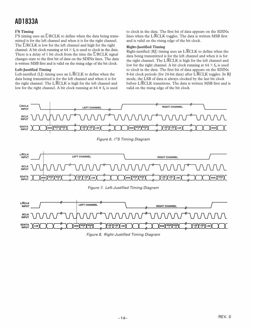
I2S TimingI2S timing uses an L/RCLK to define when the data being trans-mitted is for the left channel and when it is for the right channel.The L/RCLK is low for the left channel and high for the rightchannel. A bit clock running at 64 � fS is used to clock in the data.There is a delay of 1 bit clock from the time the L/RCLK signalchanges state to the first bit of data on the SDINx lines. The datais written MSB first and is valid on the rising edge of the bit clock.
Left-Justified TimingLeft-justified (LJ) timing uses an L/RCLK to define when thedata being transmitted is for the left channel and when it is forthe right channel. The L/RCLK is high for the left channel andlow for the right channel. A bit clock running at 64 � fS is used
LEFT CHANNEL RIGHT CHANNEL
LSB+1 LSB MSB
L/RCLKINPUT
BCLKINPUT
SDATAINPUT
LSB+2
MSB–2
MSB–1MSBLSB
+1 LSBLSB+2
MSB–2
MSB–1MSB
Figure 6. I 2S Timing Diagram
LEFT CHANNEL RIGHT CHANNEL
LSB+1 LSB
L/RCLKINPUT
BCLKINPUT
SDATAINPUT
LSB+2
MSB–2
MSB–1MSBLSB
+1 LSBLSB+2
MSB–2
MSB–1MSB MSB
–1MSB
Figure 7. Left-Justified Timing Diagram
LEFT CHANNEL RIGHT CHANNEL
LSB+1 LSB
L/RCLKINPUT
BCLKINPUT
SDATAINPUT
LSB+2
MSB–2
MSB–1LSB MSB LSB
+1 LSBLSB+2
MSB–2
MSB–1MSB
Figure 8. Right-Justified Timing Diagram
to clock in the data. The first bit of data appears on the SDINxlines when the L/RCLK toggles. The data is written MSB firstand is valid on the rising edge of the bit clock.
Right-Justified TimingRight-justified (RJ) timing uses an L/RCLK to define when thedata being transmitted is for the left channel and when it is forthe right channel. The L/RCLK is high for the left channel andlow for the right channel. A bit clock running at 64 � fS is usedto clock in the data. The first bit of data appears on the SDINx8-bit clock periods (for 24-bit data) after L/RCLK toggles. In RJmode, the LSB of data is always clocked by the last bit clockbefore L/RCLK transitions. The data is written MSB first and isvalid on the rising edge of the bit clock.
REV. 0
AD1833A
–15–
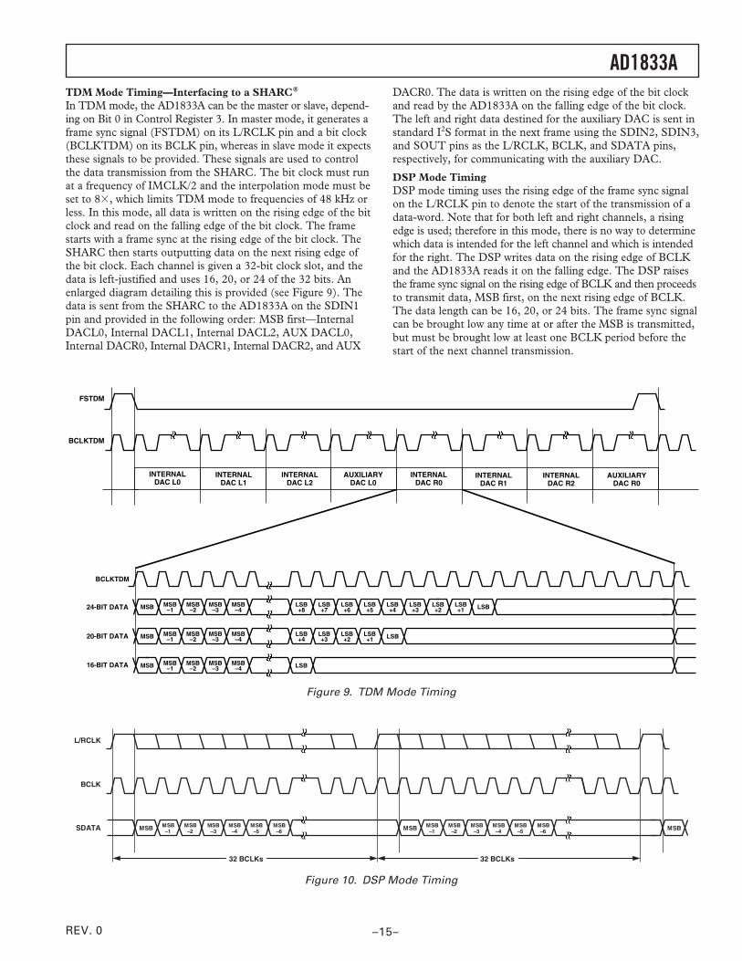
TDM Mode Timing—Interfacing to a SHARC®
In TDM mode, the AD1833A can be the master or slave, depend-ing on Bit 0 in Control Register 3. In master mode, it generates aframe sync signal (FSTDM) on its L/RCLK pin and a bit clock(BCLKTDM) on its BCLK pin, whereas in slave mode it expectsthese signals to be provided. These signals are used to controlthe data transmission from the SHARC. The bit clock must runat a frequency of IMCLK/2 and the interpolation mode must beset to 8�, which limits TDM mode to frequencies of 48 kHz orless. In this mode, all data is written on the rising edge of the bitclock and read on the falling edge of the bit clock. The framestarts with a frame sync at the rising edge of the bit clock. TheSHARC then starts outputting data on the next rising edge ofthe bit clock. Each channel is given a 32-bit clock slot, and thedata is left-justified and uses 16, 20, or 24 of the 32 bits. Anenlarged diagram detailing this is provided (see Figure 9). Thedata is sent from the SHARC to the AD1833A on the SDIN1pin and provided in the following order: MSB first—InternalDACL0, Internal DACL1, Internal DACL2, AUX DACL0,Internal DACR0, Internal DACR1, Internal DACR2, and AUX
DACR0. The data is written on the rising edge of the bit clockand read by the AD1833A on the falling edge of the bit clock.The left and right data destined for the auxiliary DAC is sent instandard I2S format in the next frame using the SDIN2, SDIN3,and SOUT pins as the L/RCLK, BCLK, and SDATA pins,respectively, for communicating with the auxiliary DAC.
DSP Mode TimingDSP mode timing uses the rising edge of the frame sync signalon the L/RCLK pin to denote the start of the transmission of adata-word. Note that for both left and right channels, a risingedge is used; therefore in this mode, there is no way to determinewhich data is intended for the left channel and which is intendedfor the right. The DSP writes data on the rising edge of BCLKand the AD1833A reads it on the falling edge. The DSP raisesthe frame sync signal on the rising edge of BCLK and then proceedsto transmit data, MSB first, on the next rising edge of BCLK.The data length can be 16, 20, or 24 bits. The frame sync signalcan be brought low any time at or after the MSB is transmitted,but must be brought low at least one BCLK period before thestart of the next channel transmission.
INTERNALDAC L0
INTERNALDAC L1
INTERNALDAC L2
AUXILIARYDAC L0
INTERNALDAC R0
INTERNALDAC R1
INTERNALDAC R2
AUXILIARYDAC R0
FSTDM
BCLKTDM
MSB24-BIT DATA
20-BIT DATA
16-BIT DATA
BCLKTDM
MSB–1
MSB–2
MSB–3
MSB–4
LSB+8
LSB+7
LSB+6
LSB+5
LSB+4
LSB+3
LSB+2
LSB+1 LSB
MSB MSB–1
MSB–2
MSB–3
MSB–4
LSB+4
LSB+3
LSB+2
LSB+1 LSB
MSB MSB–1
MSB–2
MSB–3
MSB–4 LSB
Figure 9. TDM Mode Timing
L/RCLK
BCLK
SDATA MSB MSB–1
MSB–2
MSB–4
MSB–5
MSB–6 MSB MSB
–1MSB–2
MSB–3
MSB–4
MSB–5
MSB–6 MSB
32 BCLKs32 BCLKs
MSB–3
Figure 10. DSP Mode Timing

REV. 0
AD1833A
–16–
Packed Mode 128In Packed Mode 128, all six data channels are packed into onesample interval on one data pin. The BCLK runs at 128 � fS;therefore, there are 128 BCLK periods in each sample interval.Each sample interval is broken into eight time slots: six slots of20 BCLK and two of 4 BCLK. In this mode, the data length isrestricted to a maximum of 20 bits. The three left channels arewritten first, MSB first, and the data is written on the fallingedge of BCLK. After the three left channels are written, there isa space of four BCLK, and then the three right channels are writ-ten. The L/RCLK defines the left and right data transmission; itis high for the three left channels and low for the three right channels.
Packed Mode 256In Packed Mode 256, all six data channels are packed into onesample interval on one data pin. The BCLK runs at 256 � fS;therefore, there are 256 BCLK periods in each sample interval, andeach sample interval is broken into eight time slots of 32 BCLKeach. The data length can be 16, 20, or 24 bits. The three leftchannels are written first, MSB first, and the data is written on thefalling edge of BCLK with a one BCLK period delay from thestart of the slot. After the three left channels are written, there isa space of 32 BCLK, and then the three right channels are written.The L/RCLK defines the left and right data transmission; it islow for the three left channels and high for the three right channels.
SLOT 1LEFT 0
SLOT 2LEFT 1
SLOT 3LEFT 2
BLANK SLOT4 SCLK
SLOT 4RIGHT 0
SLOT 5RIGHT 1
SLOT 6RIGHT 2
BLANK SLOT 4 SCLK
DATA
20-BIT DATA
16-BIT DATA
BCLK
BCLK
MSB–1
MSB–2
MSB–3
MSB–4
MSB–1
MSB–2
MSB–3
MSB–4
LSB+4
LSB+3
LSB+2
LSB+1
MSB LSB
LSBMSB
L/RCLK
Figure 11. Packed Mode 128
SLOT 1LEFT 0
SLOT 2LEFT 1
SLOT 3LEFT 2
SLOT 4RIGHT 0
SLOT 5RIGHT 1
SLOT 6RIGHT 2
20-BIT DATA
24-BIT DATA
16-BIT DATA
BCLK
MSB–1
MSB–2
MSB–3
MSB–4
MSB–1
MSB–2
MSB–3
MSB–4
LSB+8
LSB+7
LSB+6
LSB+5
LSB+4
LSB+3
LSB+2
LSB+1
LSB+4
LSB+3
LSB+2
LSB+1
MSB LSB
LSB
LSB
MSB
MSB–1
MSB–2
MSB–3
MSB–4MSB
DATA
BCLK
L/RCLK
Figure 12. Packed Mode 256
REV. 0
AD1833A
–17–
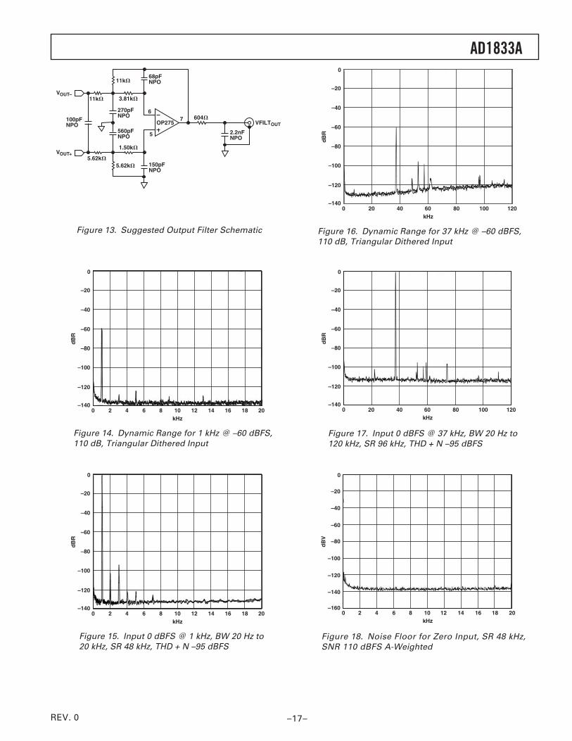
20 40 60 80
0
–20
–40
–60
–80
–100
–120
–140100 120
kHz
dB
R
0
Figure 16. Dynamic Range for 37 kHz @ –60 dBFS,110 dB, Triangular Dithered Input
20 40 60 80
0
–20
–40
–60
–80
–100
–120
–140100 120
kHz
dB
R
0
Figure 17. Input 0 dBFS @ 37 kHz, BW 20 Hz to120 kHz, SR 96 kHz, THD + N –95 dBFS
2 4 6 8
0
–20
–40
–60
–80
–100
–120
–140
10 12kHz
dB
V
0–160
14 16 18 20
Figure 18. Noise Floor for Zero Input, SR 48 kHz,SNR 110 dBFS A-Weighted
3.81k�
270pFNPO
11k�68pFNPO
11k�VOUT–
5.62k�VOUT+
560pFNPO
1.50k�
5.62k� 150pFNPO
OP275604�
2.2nFNPO
VFILTOUT
5
67100pF
NPO
Figure 13. Suggested Output Filter Schematic
2 4 6 8 10 12 14 16
0
–20
–40
–60
–80
–100
–120
–14018 20
kHz
dB
R
0
Figure 14. Dynamic Range for 1 kHz @ –60 dBFS,110 dB, Triangular Dithered Input
2 4 6 8 10 12 14 16
0
–20
–40
–60
–80
–100
–120
–14018 20
kHz
dB
R
0
Figure 15. Input 0 dBFS @ 1 kHz, BW 20 Hz to20 kHz, SR 48 kHz, THD + N –95 dBFS
REV. 0
AD1833A
–18–
–90 –80 –70 –60
–30
–40
–50
–60
–70
–80
–90
–50 –40dBFS
dB
R
–100
–100
–30 –20 –10 0
–20
–110
–120
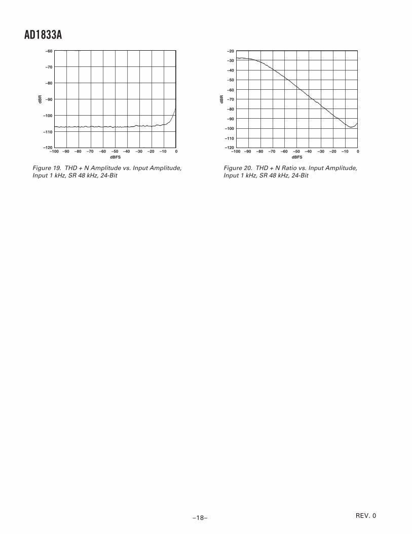
Figure 20. THD + N Ratio vs. Input Amplitude,Input 1 kHz, SR 48 kHz, 24-Bit
–90 –80 –70 –60
–70
–80
–90
–100
–50 –40dBFS
dB
R
–100 –30 –20 –10 0
–60
–110
–120
Figure 19. THD + N Amplitude vs. Input Amplitude,Input 1 kHz, SR 48 kHz, 24-Bit
REV. 0
AD1833A
–19–
CLATCHCDATACCLK
L/RCLKBCLKSDIN1SDIN2SDIN3SOUTMCLK
OUTLP1OUTLN1OUTLP2OUTLN2
OUTLP3OUTLN3
OUTRP1OUTRN1OUTRP2OUTRN2
OUTRP3OUTRN3
FILTR
FILTD
DG
ND
1
DG
ND
2
GN
D
DV
DD
1
DV
DD
2
AV
DD
1A
VD
D2
AV
DD
AV
DD
AV
DD
AD1833A
0.1�F
+
+
+
0.1�F
10�F
0.1�F
10�F
0.1�F
10�F
AVDD5V
5V
+
+
0.1�F
10�F
0.1�F
10�F
0.1�F 10�F 0.1�F 10�F++
CLATCHCDATA
CCLK
L1+L1–L2+L2–L3+L3–
R1+R1–R2+R2–R3+R3–
1247484546
363538374039
4243
14
1516
17182021222319
GN
D
GN
D
GN
D
GN
DG
ND
GN
D
+
10�F
0.1�F+
10�F
RXP
RXN
FILT
AGND
DGND
SDATAFSYNC
SCKMCK
M0M1M2M3
CU
CBLVERF
ERF
CO/EOCA/E1CB/E2CC/F0CD/F1CE/F2
SELCS12/FCK
DIR-CS8414
SHLD1
SHLD1
SHLD1
SHLD1
DV
DD
OUTU5
TORX173
10nF
10nF
47nF
1k�
75RO
5V
10k�0.1�FL5
0.1�F
10�F
26111219
23241817114152825
65432271613
8
21
20
10
9 VA
+
VD
+
5
6
2
4
1
PAL
DVD D
AVD D
7 30 6 31 5 32 41298
3
DVDD–INTF
22 7
9 28 4 33 3 34 44
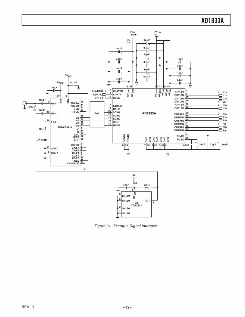
Figure 21. Example Digital Interface
REV. 0
C02
336–
0–5/
03(0
)
AD1833A
–20–
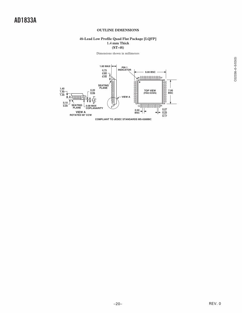
OUTLINE DIMENSIONS
48-Lead Low Profile Quad Flat Package [LQFP]1.4 mm Thick
(ST-48)
Dimensions shown in millimeters
TOP VIEW(PINS DOWN)
1
1213
2524
363748
0.27 0.22 0.17
0.50BSC
7.00BSC
SEATINGPLANE
1.60 MAX
0.750.600.45
VIEW A7�3.5�0�
0.20 0.09
1.45 1.40 1.35
0.150.05 0.08 MAX
COPLANARITY
VIEW AROTATED 90� CCW
PIN 1INDICATOR
9.00 BSC
COMPLIANT TO JEDEC STANDARDS MS-026BBC
SEATINGPLANE