Embed Size (px)
Citation preview
Multiband Hot Photoluminescence from Nanocavity-EmbeddedSilicon Nanowire Arrays with Tunable WavelengthZhiqiang Mu,† Haochi Yu,‡ Miao Zhang,† Aimin Wu,† Gongmin Qi,† Paul K. Chu,∥ Zhenghua An,*,‡,§
Zengfeng Di,*,† and Xi Wang†
†State Key Laboratory of Functional Materials for Informatics, Shanghai Institute of Microsystem and Information Technology,Chinese Academy of Sciences, Shanghai 200050, People’s Republic of China‡State Key Laboratory of Surface Physics, Department of Physics and §Collaborative Innovation Center of Advanced Microstructures,Fudan University, Shanghai 200433, People’s Republic of China∥Department of Physics and Materials Science, City University of Hong Kong, Tat Chee Avenue, Kowloon, Hong Kong, People’sRepublic of China
*S Supporting Information
ABSTRACT: Besides the well-known quantum confinement effect,hot luminescence from indirect bandgap Si provides a new andpromising approach to realize monolithically integrated siliconoptoelectronics due to phonon-assisted light emission. In this work,multiband hot photoluminescence is generated from Si nanowirearrays by introducing trapezoid-shaped nanocavities that supporthybrid photonic-plasmonic modes. By continuously adjusting thegeometric parameters of the Si nanowires with trapezoidalnanocavities, the multiband hot photoluminescence can be tunedin the range from visible to near-infrared independent of theexcitation laser wavelength. The highly tunable wavelength bandsand concomitant compatibility with Si-integrated electronics enabletailoring of silicon-based light sources suitable for next-generationoptoelectronics devices.
KEYWORDS: Hot luminescence, Si nanowires, nanocavities, surface plasmon, resonance mode, tunable wavelength
In the pursuit of higher performance, smaller powerconsumption, and lower cost per unit, Moore’s law has
been valid for complementary metal-oxide-semiconductor(CMOS) integrated circuit (IC) for decades.1 However, onthe heels of the increasing integration density and complexity ofSi CMOS, there are severe challenges including signalpropagation delay, heat dissipation, and limited bandwidthhindering the development of high-performance and low-powerdevices such as large-scale data centers and smartphones, andeven much more advanced fin field-effect transistors (FinFETs)have joined.2−4 Introduction of Si photonics to state-of-the-artICs is regarded as a promising solution to achieve largebandwidths and low energy consumption.5,6
Although photonics-based modules such as photodetectors,7
modulators,8 and optical waveguides9 have been developedusing CMOS-compatible processes, the light sources are mainlybased on III/V compound semiconductors instead of siliconbecause of the low emission efficiency of indirect bandgap Si.10
Much effort has been made to overcome this limitation, forexample, by introducing quantum confinement effects11,12 orphotonic crystals.13,14 Unfortunately, most of these approachesare not practical, especially when considering monolithicintegration into the exiting CMOS technology. For indirect
bandgap semiconductors like Si, it is more challenging becausephonons are involved in the light emission process and morecomplex radiative and nonradiative recombinations coexist andeven compete,15−17 resulting in low light emission efficiency.Taking advantage of the nanoplasmonic resonance and theassociated huge Purcell enhancement (>1000),18,19 recentbreakthroughs on developing light sources for Si photonicshave been demonstrated on direct bandgap CdS19 and indirect-bandgap Si20 by Cho et al. For indirect-bandgap Si material,when silicon nanowire is coupled with a Ω-shaped plasmoniccavity, the remarkable radiative rate enhancement of >103 withsubpicosecond lifetimes and a spontaneous emission with theenhancement rate of 103 have been demonstrated. Despite thecontroversial luminescence mechanism,21−23 this work un-doubtedly assures the prominent merits of the phonon-assistedSi hot luminescence and suggests interesting physics among thethree types of interacting species, namely charge, phonon, andcavity photon or plasmon. However, the proposed approachrelies on randomly distributed silicon nanowires instead of
Received: November 8, 2016Revised: January 10, 2017Published: January 30, 2017
Letter
pubs.acs.org/NanoLett
© 2017 American Chemical Society 1552 DOI: 10.1021/acs.nanolett.6b04675Nano Lett. 2017, 17, 1552−1558
silicon nanowire array, which is commonly adopted by thestate-of-the-art ICs, therefore, it is not a practical solution forsilicon-based light source in term of CMOS compatibility.Meanwhile, as the optical modes corresponding to Si nanowireswith fixed shape and dimension are limited, the wavelengthtunability and the spectrum range of phonon-assisted Si hotluminescence are restricted as well, which cannot meet thebroadband demand for optical communications of siliconphotonics. Furthermore, as the luminescence mechanism forplasmonic nanocavity system is still unclear,21−23 it is offundamental importance to understand the more general light-matter interaction physics in indirect semiconductor embed-ding nanocavity systems.In this work, trapezoidal nanocavities-embedded Si nanowire
arrays with controllable dimension fabricated by CMOSprocess are investigated for phonon-assisted Si hot lumines-cence. The fabrication process is similar to that of trapezoidal-shaped FinFETs, which have been recently introduced to build22 nm high-performance and low-power CMOS technology,24
though the dimension of individual Si nanowire is enlarged forbetter visibility. Hot luminescence from trapezoidal Si nanowireis found to be governed by the plasmonic cavity mode withremarkably attenuated dependence on the intrinsic density ofstate of the phonon. By adjusting the geometric parameters ofthe Si nanowires via nanofabrication process, the multiband hotphotoluminescence associated with different orders of cavitymodes can be conveniently tuned in the range from visible tonear-infrared. Meanwhile, inheriting the small mode volume ofCMOS-compatible nanowire structures, the trapezoidal Sisystem preserves a large Purcell factor (∼1 × 10²) producingenhanced luminescence. The proposed Si light source withhighly tunable wavelengths is promising to Si photonics as wellas sensing and biomedical application.The array of Si nanowires with the identical trapezoidal
structure was fabricated on a silicon-on-insulator (SOI) waferby electron beam lithography (EBL) and modified inductively
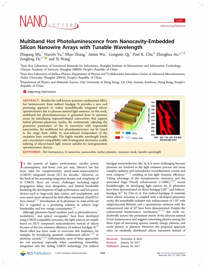
coupled plasma (ICP) etching. After transferring to a quartzsubstrate by the sacrificial etching of the buried oxide, 5 nmAl2O3 layer and 120 nm Ag layer were deposited successively toproduce the trapezoidal plasmonic nanocavity-coupled siliconnanowire device (see Supporting Information), as shown inFigure 1a,b. The plasmonic cavity was confined by the uniquehornlike metal coverage and Si/quartz interface (with arefractive index ratio of about 3.42/1.46). Transmissionelectron microscopy (TEM), scanning transmission electronmicroscopy (STEM), and energy-dispersive X-ray spectroscopy(EDS) reveal that the dielectric layer consists of 3 nm nativeoxide and 5 nm Al2O3, as shown in Figure S1 and Figure 1c.Room-temperature photoluminescence (PL) from a typical
array of trapezoidal nanocavities embedded Si nanowires withtop width Wt of 130 nm and bottom width Wb of 330 nm wasmonitored with a perpendicularly polarized 514 nm Ar laser.The laser spot size is ∼700 nm and the corresponding powerdensity is ∼2.6 mW/μm2. A broadband hot luminescencespectrum with considerable counts is observed, as shown inFigure 1d. In addition, four distinct peaks emerge from thebroadband PL spectrum of the nanocavity-embedded Sinanowires. There are at least four resonant modes along themetal/dielectrics interface perpendicular to the long axis of thenanowires. In contrast, no appreciable counts above thebackground can be detected from the array of Si nanowirescoated with the identical dielectric layers but without Agnanocavities. The difference suggests that strong confinementfrom the plasmonic trapezoidal nanocavities is responsible forthe broadband hot luminescence. To characterize the realemission color of the nanocavity-embedded Si nanowire array,confocal laser fluorescence microscopy images acquried with40× objective and 405 nm laser at single detection channel areshown in Figure 1e. The spot size of 405 nm laser is ∼520 nm,and the corresponding laser power density is ∼17.9 mW/μm2.The figure in the upper left panel is the optical image of thearray consisting of 12 individual Si nanowires and the other
Figure 1. (a) Schematic of the trapezoidal nanocavity-embedded Si nanowire array. (b) Cross-sectional STEM image of nanocavities-embedded Sinanowire array. (c) Enlarged STEM image of a single nanocavity-embedded Si nanowire with SiO2/Al2O3/Ag coating and EDS maps of Si, Al, O,and Ag of the nanocavity-embedded Si nanowire. The red rectangular area in the STEM image is selected for EDS mapping. Scale bar: 50 nm. (d)Room-temperature PL spectra of the Si nanowires with/without Ag-coated trapezoidal nanocavities. (e) Optical (upper left) and confocal laserfluorescence microscopy images of the Si nanowire array. The wavelength of excitation laser is 405 nm and the scale bar is 8 μm.
Nano Letters Letter
DOI: 10.1021/acs.nanolett.6b04675Nano Lett. 2017, 17, 1552−1558
1553
three figures are the corresponding confocal laser fluorescenceimages obtained using 525, 585, and 650 nm channels,respectively. Three fluorescence images also show the align-ment of silicon nanowires but three different colors of green,yellow, and red, which are consistent with three strong hotluminescence bands in the visible region, as shown in Figure 1d.In addition, the fouth strong hot luminescence band at 793 nm,which is located in the near-infrared region, cannot be resolvedby confocal laser fluorescence microscopy. Other than thesilicon nanowire array, the more complex pattern “SIMIT”(abbreviation of our institute) composed of silicon nanowirescan be fabricated (Figure S2) and each letter shows broadbandhot luminescence. The letter “SIMIT” can be selectivelydisplayed by PL mapping of the luminescence peak, forexample, at 650 and 750 nm.Room-temperature PL is monitored with four different laser
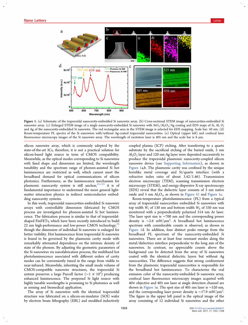
lines of 405, 514, 532, and 633 nm to characterize thenanocavity-embedded Si nanowires. As shown in Figure 2a, thepeak positions are always fixed irrespective of the energy of theexcitation laser. It is similar to the usual light emission of near-band-edge combination but different from that observed fromΩ-shaped cavities.21 This implies that in the trapezoidal Sinanowires, radiative recombination of excited carriers occurs atthe resonance frequencies of the cavity modes involving realelectronic states (not necessarily to be band minima such as X,L in electronic band diagram). In contrast, involvement of thereal or virtual electronic states has to be precautiously justifiedin Ω-cavities in order to be distinguished from resonant Ramanprocess.23 The cavity modes for a particular nanowire arespectrally fixed by its geometry and the tunability of hotluminescence from the trapezoidal cavity embedded Sinanowires can be inferred. For different batches of nanowires
with the same size, the luminescence bands are alwaysindependent of the laser excitation energy and it is ratherimportant to attain tunable luminescence by engineering thecavity resonances later.To investigate the origin of hot luminescence, the nano-
cavity-embedded Si nanowire array is studied by monitoring thePL spectra at different temperatures, as shown in Figure 2b.The photoluminescence intensity is enhanced as the measure-ment temperature is increased from 77 to 300 K and theintegrated intensity in the PL spectrum at 300 K is 5−10 timeslarger than that in the 77 K one. Therefore, the hotluminescence of nanocavity-embedded Si nanowire arrayexhibits a positive temperature dependence, which is contraryto that of direct bandgap materials like AlGaAs25 and CdS.26
The photoluminescence from direct bandgap materials isalways suppressed at elevated temperature due to increasednonradiative recombination.27 However, the process for hotluminescence from an indirect bandgap material (Si intrapezoidal cavities) is quite different, where the thermallyactivated phonons are necessary to mediate radiativerecombination and satisfy momentum conservation. As thephonon population increases with temperature,28 the hotluminescence from the nanocavity-embedded Si nanowire arrayis enhanced at elevated temperature accordingly. Previously, thesimilar positive temperature dependence of photoluminescencebehavior has been observed in Ω-shaped plasmonically coupledSi nanowires21,23 in which phonon mediated radiativerecombination dominates. It is worth mentioning that theenhanced absorption coefficient of silicon at elevated temper-ature may also contribute to the increased PL intensity to someextent (∼2.4 fold at most) but should not be the dominatingreason as determined by the more quantitative analysis.21
Figure 2. (a) Room-temperature PL spectra of the trapezoidal nanocavity-embedded Si nanowire array excited by 405, 514, 532, and 633 nm laserlines. Each spectral curve has been normalized and offset for clarity purpose. (b) PL spectra of the trapezoidal nanocavity-embedded Si nanowirearray at 77 and 300 K. (c) Room-temperature PL intensity of the trapezoidal nanocavity-embedded Si nanowire array as a function of excitationpower. The inset shows the corresponding PL spectra with different excitation power of the 514 nm laser. (d) Time-resolved hot luminescence decayof the plasmonic Si nanowire (with Ag coating) and the photonic Si nanowire (without Ag coating) at room temperature. The emission lifetime isextracted from the exponential fitting curve.
Nano Letters Letter
DOI: 10.1021/acs.nanolett.6b04675Nano Lett. 2017, 17, 1552−1558
1554
The change in the PL intensity with excitation power isalways investigated to study the recombination process forabove-band gap excitation, especially for II−VI and III−Vcompound direct bandgap semiconductors.29−31 The powerdependence of the PL intensity can be described by an I ∼ Pα
law, where I is the luminescence intensity, P is the excitationlaser power, and α is a dimensionless exponent.29−31 Withregard to the free- and bound-exciton emission, α is generallybetween 1 and 2 but is usually less than 1 for free to bound anddonor−acceptor pair recombination. The PL spectra areacquired using a 514 nm laser with different excitation powerat room temperature. The PL intensity at around 790 nmincreases with excitation power as shown in the inset in Figure2c. It follows a similar trend as the aforementioned directbandgap semiconductors with α of ∼0.6. The sublinearity ofthe luminescence intensity with increasing pump power may becaused by the dynamic equilibrium between hot carrierradiation and intraband relaxation. The similarity of thetrapezoidal Si (α ∼ 0.6) with free-to-bound and donor−acceptor pair recombination in direct bandgap semiconductors(α < 1) suggests that the hot luminescent process is complexinvolving phonons. The reported I ∼ Pα law is generally appliedto direct bandgap semiconductor but it is noted that thecomprehensive theory is still absent and has to be developed inthe future to describe the nonlinear power dependence of hotcarrier luminescence from nanocavity-embedded Si nanowires.The interactions among three particle systems (carriers,phonons, and cavity plasmons) and other nonlinear process(phonon intraband relaxation and Auger recombination) mustbe taken into account.To confirm the radiative recombination enhancement, the
time-resolved hot luminescence decay of cavity-embedded Sinanowires is monitored using time-correlated single photon
counting (TCSPC) system in the emission range between 630and 730 nm at pulsed excitation of λex = 405 nm (Figure 2d).TCSPC system is extremely sensitive for weak emission, and itcan even detect the spontaneous emission from photonic SiNWs without plasmonic nanocavity although it requiressufficiently long time to achieve reasonable photon counts.The light emission for plasmonic Si nanowires, that is,trapezoidal nanocavity-embedded Si nanowires with Ag coatingexhibits an exponential decay with a spontaneous emissionlifetime of ∼130 ps. It is reduced by a factor of 45 incomparison with photonic Si nanowires, that is, trapezoidal Sinanowires without Ag coating (∼5.9 ns). The lifetime appearsto be very short compared to previous reports on indirectbandgap Si systems28 but comparable to direct bandgapsemiconductors such as the hybrid CdS−MgF2−Ag nano-squares (∼72 ps).32 The large radiative rate enhancement isbelieved to be caused by the ultrasmall mode volumes andreasonably high quality factors of the nanocavities that providehigh electromagnetic energy densities.To further investigate the enhanced electromagnetic field
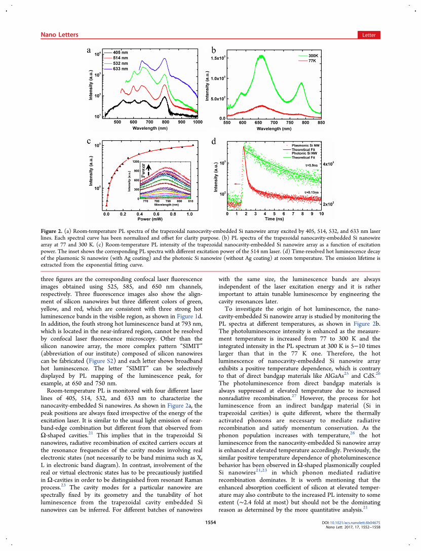
intensity in the cavity-embedded Si nanowire, finite-differencetime-domain (FDTD) simulation is performed. The simulatedfrequency-dependent electromagnetic field intensity inside thenanocavity is enhanced at 532, 596, 677, and 792 nm (Figure3a), indicating four resonance modes (I−IV) produced by thenanocavity. These peaks match well with four hot luminescencepeaks obtained by the experimental PL results. The agreementbetween the simulation results and the experimental datasuggests that radiative recombination of excited carriers occursmainly at the resonance frequency of the cavity modes,suggesting that it is feasible to tailor the luminescentwavelengths by changing the dimensions of the cavities. Asexpected, the calculated electric and magnetic field profiles of
Figure 3. (a) Calculated frequency-dependent electromagnetic field intensity inside the nanocavity of the trapezoidal Si nanowire with theexperimental PL spectrum included for comparsion. The four resonance modes labeled as I, II, III, and IV are observed. (b,c) The calculated electricand magnetic field profiles for resonance modes I, II, III, and IV, respectively.
Nano Letters Letter
DOI: 10.1021/acs.nanolett.6b04675Nano Lett. 2017, 17, 1552−1558
1555
the four resonant cavity modes (I−IV) show that theelectromagnetic field is not only confined in the gap regionbetween the metal surface and Si nanowires, but also moreimportantly inside the Si nanowires (Figure 3b,c) thusenhancing the light-matter (Si) interaction. The resonantmodes verify that the confinement by the Ag and Si/quartzinterface is sufficient even though the Si/quartz interface allowsmoderate transmission. The electromagnetic field of a puresurface plasmon state is confined to the metal surface withexponentially decaying profiles away from the metal sufarce andso there is large metallic ohmic loss. In our trapezoidalnanocavities, however, the plasmonic resonant modes arehybridized with photonic ones and a significant portion of theelectromagnetic field is located inside the nanowire tocontribute to the light-matter (Si) interaction. Because theelectric field is preferentially perpendiular to the long axis of thenanowire in the hybrid plasmonic modes, the parallel polarizedPL intensity is suppressed giving rise to the obviouspolarization dependence on emission polarization (FigureS3). For comparison, the polarization dependence of excitationpolarization shows no clear difference, and experiments (FigureS4) under parallel (photonic-like) and perpendicular (plas-monic-like) excitations show comparable luminescent inten-sities, which agrees well with earlier work with large sizenanowire.21 The experimental observation is also consistentwith our theoretical simulations that predicts comparable Siabsorption efficiencies under parallel/perpendicular laserexcitations at 514 nm (not shown). Because the hotluminescence from Si is an inelastic and incoherent process,the PL signal becomes nearly independent of the excitationpolarization once the excitation energy is absorbed by theembedded Si. Consequently, the PL intensity is justified by thePurcell enhancement effect21 that prefers the plasmonic-like
modes and therefore perpendicular emission polarization. Thestronger dependence of hot luminescence on emissionpolarization rather than excitation polarization suggests thatthe optical cavity modes in lieu of the intrinsic density ofphonon state play a crucial role in the hot luminescent emissionfrom the trapezoidal samples.The spontaneous emission rate enhancement of a dipole
source observed by Purcell33 is given by
γγ π
λ= =
⎛⎝⎜
⎞⎠⎟
⎛⎝⎜
⎞⎠⎟F
nQV
34P
02
c3
m
where γ and γ0 are the spontanous emssion rates in the hostmedium and free space, respectively, and λc, n, Q, and Vm arethe vacuum wavelength, refractive index, quality factor, andmode volume, respectively.17,34 The spontaneous emission rateenhancement known as the Purcell effect is determined by Qand Vm. As the optical cavity has entered into nanoscale, thequality factor of the cavity mode Q is reduced slightly (less than102) compared to the microscale counterpart. However, themode volume Vm shrinks more dramatically, thus resulting in alarger FP. Therefore, enhanced spontaneous emission can beachieved from the ultrasmall optical cavity. The quality factor Qof the hybrid cavity mode is estimated to be ∼60 with thefrequency at around 792 nm (mode IV in Figure 3a) and modevolume of λc
3/103 (λc is the free-space wavelength).35 It leads to
a Purcell factor of ∼1 × 10², which is the same magnitude asthat reported by Mokkapati et al.35
The luminescence property of the trapezoidal nanocavityembedded Si nanowires is determined by the cavity modesinstead of the intrinsic phonon band structure. Therefore, theluminescence band of the nanocavity-embedded Si nanowirescan be easily tuned by changing the dimensions of the Si
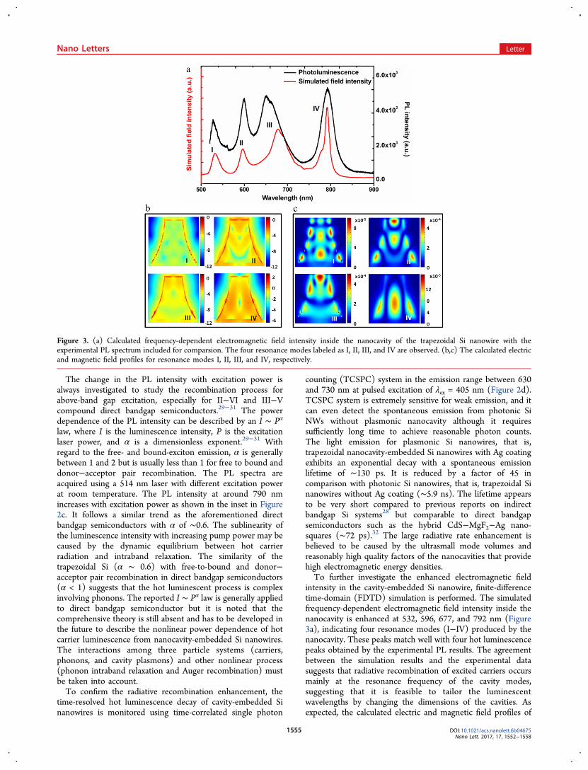
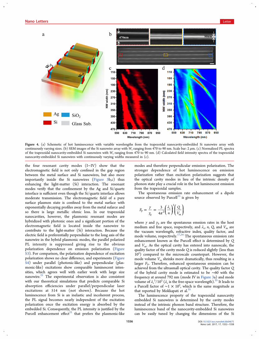
Figure 4. (a) Schemetic of hot luminescence with variable wavelengths from the trapezoidal nanocavity-embedded Si nanowire array withcontinuously varying sizes. (b) SEM images of the Si nanowire array withWt ranging from 470 to 90 nm. Scale bar: 2 μm. (c) Normalized PL spectraof the trapezoidal nanocavity-embedded Si nanowires with Wt ranging from 470 to 90 nm. (d) Calculated field intensity spectra of the trapezoidalnanocavity-embedded Si nanowires with continuously varying widths measured in (c).
Nano Letters Letter
DOI: 10.1021/acs.nanolett.6b04675Nano Lett. 2017, 17, 1552−1558
1556
nanowires. When the size of the nanocavity is changedcontinuously, the nanocavity resonance modes are expectedto shift gradually, as schematically illustrated in Figure 4a. As aresult of the precise CMOS nanofabrication process, Ag/SiO2layer-coated Si trapezoidal nanocavity arrays with continuouslyvarying widths between 90 and 470 nm are fabricated (Figure4b). The normalized PL spectra (Figure 4c and Figure S5)show that the luminescence bands shift to lower wavelength(blue shift) as the top width of the trapezoidal nanocavity Wtdecreases. In particular, as Wt is changed from 470 to 90 nm,the three typical luminsecent peaks shift from ∼750 to ∼550nm, ∼870 to ∼630 nm, and ∼900 to ∼670 nm, correspondingto the tunability ratios of about 31%, 32%, and 29%,respectively. Moreover, four distinct emission peaks emergefrom the nanocavities with large Wt (430 nm < Wt < 470 nm).As the top width of the trapezoidal nanocavity Wt is decreased,the two emission peaks at lower wavelengths (630−750 nm)merge into a single peak, while the other two emission peaks athigher wavelengths (790−880 nm) merges first and then splits.The luminescence band evolution is also revealed by numericalsimulation of the field intensity as a function of nanowire size,as shown in Figure 4d. Considering the dispersive refractiveindex of Si in this wide wavelength range and also imperfectionin nanofabrication, the agreement between the simulation(Figure 4d) and experimental data (Figure 4c) is quite good. Inaddition, the polarization-dependent data (Figure S6) showconsistency with the cavity mode simulation, which furtherproves that wavelength tuning indeed originates from the cavitymodes, because the electronic band and phonon density ofstates are both fixed in the gradient nanowires. Most of theluminescent range (600−950 nm) in Figure 4c is below the L-point bandgap but still above the X-point bandgap and theluminescence thus arises from hot electrons along the Γ−Xelectronic branch and no peak emission is shown withoutregulation by the photon or phonon density of states. Inpractice, the trapezoidal cavity resonances (Figure 4d) show upin the same wavelength range and exhibit a similar blue shifttendency with decreasing cavity size, producing evidence thatphoton rather than phonon density of states plays a crucial rolehere.As shown by the experimental and simulation results in
Figure 4, the luminescence bands of the Si nanowires withtrapezoidal nanocavities can be tuned by the cavity resonancemodes. Thus, the wavelength of the emission peaks can besimply tuned by designing the Si nanowires with particulardimensions. For a Ω-shaped cavity, the plasmonic cavity modescan also be adjusted by changing the diameter of the Sinanowires. Nevertheless, the strong hot luminescence bands ofSi nanowires are fixed at around 2.51, 2.34, and 2.18 eV withoutany shift when perfect matching is satisfied between cavityresonances and phonons with the largest density of states.20,21
In the trapezoidal nanocavities, hot electrons emitted at alonger wavelength range (600−950 nm) exhibit largermomentum mismatch and therefore require participation ofmultiple phonons. Because of the multiple-phonon involvementand many possible pathways, the spectral features modulated byspecific phonon with high density of states becomes lessnoticeable and the spectral tunability by cavity modes becomesprominent compared to Ω-shaped cavity.20,21 Furthermore,when the nanowire is optically excited, electrons may be excitedwith higher efficiency. The hot phonon population andsubsequent phonon bottleneck of carrier relaxation mayemerge. It is believed that nonequilibrium distributed phonons
produced by hot carriers can be reabsorbed by the relaxingcharge carriers to retard the charge carriers relaxation process.As the time for radiative recombination is sufficiently shortenedby the cavity modes, the dependence of the intrinsic phononswith a large density of states will be reduced, as suggested bythe weaker temperature dependence of hot luminescence.36−38
Our work together with existing works reveals the rich physicsof hot electron relaxation dynamics interacting with other(quasi-)particles such as phonon and cavity-photon/plasmon,and the realized tunable emission in this work implies the newpossibility to engineer the luminescent property of indirectsemiconductor with the advanced nanotechnology.In conclusion, we demonstrate large enhancement in the hot
luminescence from Si nanowire arrays embedded withtrapezoidal nanocavities fabricated by CMOS-compatibleprocesses. The luminescence from trapezoidal nanocavity-embedded Si nanowire arrays has unique properties includinga very short radiative lifetime (∼130 ps), positive temperaturedependence, power law dependence on excitation laser power(I ∼ Pα, with α ∼ 0.6), and most importantly, wide wavelengthtunability with cavity resonance, which is in contrast to thephonon-dominated Ω-shaped Si nanowire case. The independ-ence of the hot luminescence bands with excitation laser showsthat hot carrier radiation recombination in the trapezoidalcavity-embedded Si nanowires is not restricted by the intrinsicphonon density of states. The hot luminescence bands can beconveniently tuned via cavity resonance modes by simplydimension adjustment of Si nanowires. The excellent wave-length tunability of trapezoidal Si nanowire system is expectedto promote its potential for future Si photonics, sensing, andbiomedical research applications.
■ ASSOCIATED CONTENT*S Supporting InformationThe Supporting Information is available free of charge on theACS Publications website at DOI: 10.1021/acs.nano-lett.6b04675.
Experimental methods, luminescence spectra images andFDTD simulation results (PDF)
■ AUTHOR INFORMATIONCorresponding Authors*E-mail: [email protected].*E-mail: [email protected] Di: 0000-0002-9357-5107Author ContributionsZ.D. and X.W. supervised the project. Z.D., M.Z., Z.A., andZ.M. conceived and designed the experiments. Z.D. and Z.M.fabricated the samples and carried out experimental measure-ments. H.Y., G.Q., and Z.A. performed the FDTD simulation.Z.D., Z.A., A.W., P.K.C., Z.M., and H.Y. analyzed the data andcowrote the paper. All the authors discussed the results andcommented on the manuscript. Z.M. and H.Y. contributedequally to this work.NotesThe authors declare no competing financial interest.
■ ACKNOWLEDGMENTSThe authors thank the financial support from National NaturalScience Foundation of China (61274136/11427807/
Nano Letters Letter
DOI: 10.1021/acs.nanolett.6b04675Nano Lett. 2017, 17, 1552−1558
1557
11634012/11674070), Creative Research Groups of NationalNatural Science Foundation of China (No. 61321492),Program of Shanghai Academic/Technology Research Leader(16XD1404200), and City University of Hong Kong AppliedResearch Grant (ARG) 9667122.
■ REFERENCES(1) Chau, R.; Doyle, B.; Datta, S.; Kavalieros, J.; Zhang, K. Nat.Mater. 2007, 6, 810−812.(2) del Alamo, J. A. Nature 2011, 479, 317−323.(3) Frank, D. J. IBM J. Res. Dev. 2002, 46, 235−244.(4) Theis, T. N.; Solomon, P. M. Proceedings of the IEEE 2004International Interconnect Technology Conference 2010, 98, 2005−2014.(5) Chen, X.; Li, C.; Tsang, H. K. NPG Asia Mater. 2011, 3, 34−40.(6) Sun, C.; Wade, M. T.; Lee, Y.; Orcutt, J. S.; Alloatti, L.; Georgas,M. S.; Waterman, A. S.; Shainline, J. M.; Avizienis, R. R.; Lin, S.; Moss,B. R.; Kumar, R.; Pavanello, F.; Atabaki, A. H.; Cook, H. M.; Ou, A. J.;Leu, J. C.; Chen, Y. H.; Asanovic, K.; Ram, R. J.; Popovic, M. A.;Stojanovic, V. M. Nature 2015, 528, 534−538.(7) Assefa, S.; Xia, F. N. A.; Vlasov, Y. A. Nature 2010, 464, 80−84.(8) Xu, Q. F.; Schmidt, B.; Pradhan, S.; Lipson, M. Nature 2005, 435,325−327.(9) Xia, F. N.; Sekaric, L.; Vlasov, Y. Nat. Photonics 2007, 1, 65−71.(10) Liu, J. F.; Camacho-Aguilera, R.; Bessette, J. T.; Sun, X. C.;Wang, X. X.; Cai, Y.; Kimerling, L. C.; Michel, J. Thin Solid Films 2012,520, 3354−3360.(11) Cullis, A. G.; Canham, L. T. Nature 1991, 353, 335−338.(12) Wilson, W. L.; Szajowski, P. F.; Brus, L. E. Science 1993, 262,1242−1244.(13) Akahane, Y.; Asano, T.; Song, B. S.; Noda, S. Nature 2003, 425,944−947.(14) Fujita, M.; Takahashi, S.; Tanaka, Y.; Asano, T.; Noda, S. Science2005, 308, 1296−1298.(15) Goldman, J. R.; Prybyla, J. A. Phys. Rev. Lett. 1994, 72, 1364−1367.(16) Liang, D.; Bowers, J. E. Nat. Photonics 2010, 4, 511−517.(17) Aspetti, C. O.; Agarwal, R. J. Phys. Chem. Lett. 2014, 5, 3768−3780.(18) Bergman, D. J.; Stockman, M. I. Phys. Rev. Lett. 2003, 90,027402.(19) Cho, C. H.; Aspetti, C. O.; Turk, M. E.; Kikkawa, J. M.; Nam, S.W.; Agarwal, R. Nat. Mater. 2011, 10, 669−675.(20) Cho, C. H.; Aspetti, C. O.; Park, J.; Agarwal, R. Nat. Photonics2013, 7, 285−289.(21) Aspetti, C. O.; Cho, C. H.; Agarwal, R.; Agarwal, R. Nano Lett.2014, 14, 5413−5422.(22) Russell, K. J.; Hu, E. L. Nat. Photonics 2014, 8, 666−666.(23) Aspetti, C. O.; Cho, C. H.; Park, J.; Agarwal, R. Nat. Photonics2014, 8, 667−668.(24) Intel Corporation. 3-D, 22nm: New TechnologyDelivers AnUnprecedented Combination ofPerformance and Power Efficiency. www.intel.com/content/www/us/en/silicon-innovations/intel-22nm-technology.html.(25) Titova, L. V.; Hoang, T. B.; Jackson, H. E.; Smith, L. M.;Yarrison-Rice, J. M.; Kim, Y.; Joyce, H. J.; Tan, H. H.; Jagadish, C.Appl. Phys. Lett. 2006, 89, 173126.(26) Hoang, T. B.; Titova, L. V.; Jackson, H. E.; Smith, L. M.;Yarrison-Rice, J. M.; Lensch, J. L.; Lauhon, L. J. Appl. Phys. Lett. 2006,89, 123123.(27) Pankove, J. I. Optical processes in semiconductors; Prentice-Hall:Englewood Cliffs, NJ, 1971.(28) Kwack, H. S.; Sun, Y.; Cho, Y. H.; Park, N. M.; Park, S. J. Appl.Phys. Lett. 2003, 83, 2901−2903.(29) Cooper, D. E.; Bajaj, J.; Newman, P. R. J. Cryst. Growth 1988,86, 544−551.(30) Schmidt, T.; Lischka, K.; Zulehner, W. Phys. Rev. B: Condens.Matter Mater. Phys. 1992, 45, 8989−8994.
(31) Daoudi, M.; Kaouach, H.; Dhifallah, I.; Ouerghi, A.; Chtourou,R. Optik 2015, 126, 932−936.(32) Ma, R. M.; Oulton, R. F.; Sorger, V. J.; Bartal, G.; Zhang, X. Nat.Mater. 2011, 10, 110−113.(33) Purcell, E. M. Phys. Rev. 1946, 69, 37.(34) Piccione, B.; Aspetti, C. O.; Cho, C. H.; Agarwal, R. Rep. Prog.Phys. 2014, 77, 086401.(35) Mokkapati, S.; Saxena, D.; Jiang, N.; Li, L.; Tan, H. H.; Jagadish,C. Nano Lett. 2015, 15, 307−312.(36) Nozik, A. J. Annu. Rev. Phys. Chem. 2001, 52, 193−231.(37) Tea, E.; Hamzeh, H.; Aniel, F. J. Appl. Phys. 2011, 110, 113108.(38) Conibeer, G.; Patterson, R.; Huang, L. M.; Guillernoles, J. F.;Konig, D.; Shrestha, S.; Green, M. A. Sol. Energy Mater. Sol. Cells 2010,94, 1516−1521.
Nano Letters Letter
DOI: 10.1021/acs.nanolett.6b04675Nano Lett. 2017, 17, 1552−1558
1558

Supporting Information for
Multiband Hot Photoluminescence from Nanocavity-Embedded
Silicon Nanowire Arrays with Tunable Wavelength
Zhiqiang Mu†, Haochi Yu
‡, Miao Zhang
†, Aiming Wu
†, Gongmin Qi
†, Paul K. Chu
||,
Zhenghua An*,‡,§
, Zengfeng Di*,†
, Xi Wang†
† State Key Laboratory of Functional Materials for Informatics, Shanghai Institute of
Microsystem and Information Technology, Chinese Academy of Sciences, Shanghai
200050, People's Republic of China
‡ State Key Laboratory of Surface Physics, Department of Physics and
§ Collaborative
Innovation Center of Advanced Microstructures, Fudan University, Shanghai 200433,
People's Republic of China
|| Department of Physics and Materials Science, City University of Hong Kong, Tat
Chee Avenue, Kowloon, Hong Kong, People's Republic of China
Methods
Device fabrication and characterization
The 25 μm long Si nanowire array was fabricated on an undoped SOI substrate
with a top Si layer of 190 nm and buried oxide (BOX) of 145 nm by electron beam
lithography (EBL) and inductively coupled plasma (ICP) etching. The trapezoidal
structure was formed purposely during ICP by using SF6 gas but without CF4
passivation gas. The top width of Si nanowire with the trapezoidal structure was
controlled precisely by the lithographic process. After etching the undernearth BOX
layer using HF solution, the Si nanowire array was transferred to a 50 μm-thick quartz
substrate. A 5 nm Al2O3 dielectric layer was deposited by atomic layer deposition
(ALD) (Beneq TFS 200) at 200 oC using trimethyl aluminum (Al(CH3)3) as the metal
precursor and O2 as the oxidant after the growth of 3 nm native oxide on the nanowire,
which was used as a blocking layer to reduce propagation loss from the metal while
maximizing the nanocavity electromagnetic fields at the interface. Finally, 120 nm
Ag was deposited by magnetron sputtering at the rate of 0.6Å/s at room temperature
to form the plasmonic Si nanowire array. The Si nanowire array without Ag
deposition (photonic Si nanowire array) was prepared for comparison. The whole
structure of plasmonic Si nanowire, i.e., trapezoidal nanocavitie-embedded Si
nanowire with Ag coating is revealed by transmission electron microscopy (TEM), as
shown in Figure S1. For Si trapezoidal nanocavity arrays with continuously varying
widths shown in Figure 4, only 3 nm native oxide was used as a blocking layer
between Si nanowire and Ag coating to reduce propagation loss from the metal while
maximizing the nanocavity electromagnetic fields at the interface.
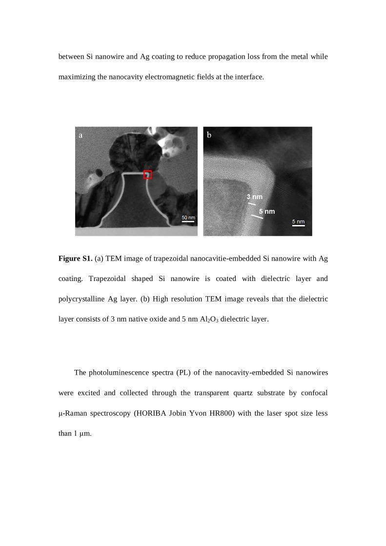
Figure S1. (a) TEM image of trapezoidal nanocavitie-embedded Si nanowire with Ag
coating. Trapezoidal shaped Si nanowire is coated with dielectric layer and
polycrystalline Ag layer. (b) High resolution TEM image reveals that the dielectric
layer consists of 3 nm native oxide and 5 nm Al2O3 dielectric layer.
The photoluminescence spectra (PL) of the nanocavity-embedded Si nanowires
were excited and collected through the transparent quartz substrate by confocal
μ-Raman spectroscopy (HORIBA Jobin Yvon HR800) with the laser spot size less
than 1 μm.
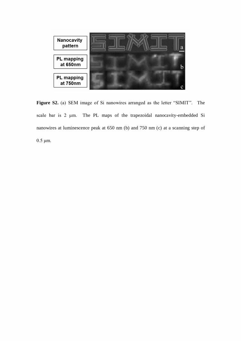
Figure S2. (a) SEM image of Si nanowires arranged as the letter “SIMIT”. The
scale bar is 2 μm. The PL maps of the trapezoidal nanocavity-embedded Si
nanowires at luminescence peak at 650 nm (b) and 750 nm (c) at a scanning step of
0.5 μm.
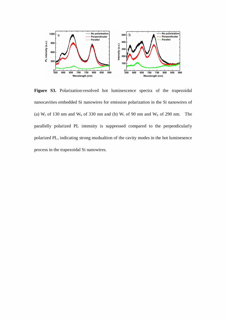
Figure S3. Polarization-resolved hot luminescence spectra of the trapezoidal
nanocavities embedded Si nanowires for emission polarization in the Si nanowires of
(a) Wt of 130 nm and Wb of 330 nm and (b) Wt of 90 nm and Wb of 290 nm. The
parallelly polarized PL intensity is suppressed compared to the perpendicularly
polarized PL, indicating strong mudualtion of the cavity modes in the hot luminesence
process in the trapezoidal Si nanowires.
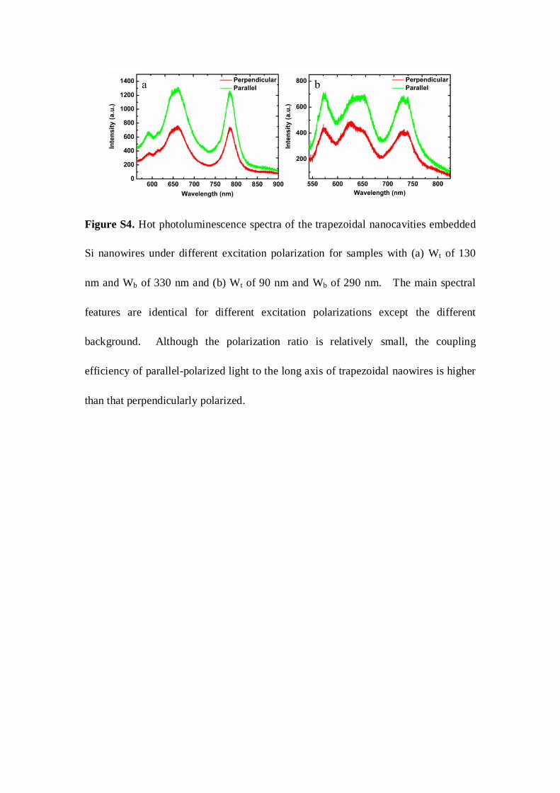
Figure S4. Hot photoluminescence spectra of the trapezoidal nanocavities embedded
Si nanowires under different excitation polarization for samples with (a) Wt of 130
nm and Wb of 330 nm and (b) Wt of 90 nm and Wb of 290 nm. The main spectral
features are identical for different excitation polarizations except the different
background. Although the polarization ratio is relatively small, the coupling
efficiency of parallel-polarized light to the long axis of trapezoidal naowires is higher
than that perpendicularly polarized.

Figure S5. PL spectra of the trapezoidal nanocavities embedded Si nanowires with
continuously changing width from 470 nm to 395 nm. The typical hot luminescence
bands of Si nanowires exhibits a blue shift from ~725 nm to ~680 nm. It is shown
experimentally that the luminescence bands of the Si nanowires with trapezoidal
nanocavities can be tuned by the cavity resonance modes. Hence, the wavelength of
the emission peaks can be tuned by designing the Si nanowires with particular
dimensions.

Figure S6. (a) Polarization-dependent PL spectra of the trapezoidal nanocavities
embedded Si nanowires with continuouly changing widths (395 nm < Wt < 470 nm)
as shown in Fig. S5. (b) Corresponding polarization ratio. The relatively large
emission polarization ratio of about 0.77 confirms that the luminescence bands of the
Si nanowires with trapezoidal nanocavities can be tuned by the cavity resonance
modes.


