Embed Size (px)
Citation preview
International Journal of Advanced Research in Computer Engineering & Technology (IJARCET)
Volume 3 Issue 10, October 2014
3577
ISSN: 2278 – 1323 All Rights Reserved © 2014 IJARCET
Multi Resonant Stacked Micro Strip Patch
Antenna Designs for IMT, WLAN &
WiMAX Applications
Tejinder Kaur Gill, Ekambir Sidhu
Abstract: In this paper, stacked multi resonant slotted
micro strip patch antennas (MPA) have been proposed
which are suitable to be used for GSM, WLAN
standard and WiMAX applications. The antennas
have been designed using substrate of FR4 material. In
the designed antennas, substrates having different
thickness have been used. The performance of designed
antenna has been observed by comparing without air
gap between the stacks with same antenna having air
gap of 0.8 mm between two stacks. It has been observed
that air gap in stacking results in increase of antenna
impedance bandwidth. The bottom stack of designed
antenna has a radiating patch of circular shape and the
patch on the upper stack is of rectangular shape. The
antenna has a feed line which is connected to circular
patch. The designed antennas have a defected ground
structure in order to improve the antenna performance.
The antenna performance has been measured in terms
of antenna parameters such as impedance bandwidth,
Return loss, antenna impedance, VSWR and
Directivity. The designed antenna results have been
simulated in CST Microwave Studio 2010. The
practically designed antennas have been tested
successfully by using Network analyzer E5071C. It has
been observed that the practical results closely match
with theoretical results.
Index Terms— Defected ground structure, Directivity,
Micro strip patch antenna, Multi resonant air gap stacked
antenna, Return loss (S11), VSWR.
Tejinder Kaur Gill, Department of Electronics & Communication
Engineering, Punjabi University Patiala., India ,+919041806381
Ekambir Sidhu, Department of Electronics and
Communication Engineering, Punjabi University, Patiala, India, 84275299711.
I. INTRODUCTION
Microstrip antenna, also known as printed circuit antenna
or patch antenna is suitable for conformal and low profile
applications. The Microstrip Patch Antenna has advantage
of low cost and weight, design flexibility and ease of
installation [4]. The radiating elements together with feed
line are photo etched on a thin dielectric sheet on a ground
plane. The patch can be square, rectangular or circular in
shape. However, MPA suffers from disadvantage that they
have narrow bandwidth. Extensive research has been
carried out to overcome the band width problem in recent
years and many techniques have been suggested and
implemented to achieve the desired wide band
characteristics [2]-[3]. One of these techniques is stacked
antennas, realizing dual frequency operation with two
resonant frequencies separated by certain range [8]-[9].
Stacked patch antenna is a kind of microstrip antenna
which consists of two printed antennas. The lower
patch is called driven patch and another patch is
parasitically coupled to driven patch. To produce
broadband responses, the selection of the substrate of the
first layer is very important.
.
Section II (Antenna Geometry) explains the geometry of
antenna. The top view, bottom view and dimensions of
substrate, patch, slots on the patch and ground plane are
listed in section II.
Section III (Results and Discussions) describes the
simulated results obtained by using CST MWS (2010)
which includes Return loss (S11), Directivity, Gain at
corresponding resonant frequencies, VSWR and Smith
chart plots.
Section IV (Experimental verification) indicates the top and
bottom view of practically designed antenna and describes
practical results obtained by testing the practically designed
antenna using E5071C ENA series Network Analyzer.

International Journal of Advanced Research in Computer Engineering & Technology (IJARCET)
Volume 3 Issue 10, October 2014
3578
ISSN: 2278 – 1323 All Rights Reserved © 2014 IJARCET
Section V (conclusion) explains both simulated theoretical
results and practical results in terms of return loss at
corresponding resonant frequencies and bandwidth, along
with list of applications in which designed antenna
can be used.
II . ANTENNA GEOMETRY
Fig. 1 shows the top view of the bottom stack of the
antenna. The Fig1 shows circular slotted patch, excited
by feedline of suitable width. Fig. 2 represents the top
view of upper stack. Fig. 3 represents the bottom view of
stacked antenna. The ground has been designed at the
bottom of the lower stack which has been partially
reduced. The antenna has been fabricated using FR4 as an
substrate with dielectric constant of 4.4.The height of
lower substrate is 1.57mm and that of upper substrate is
0.8mm.The feedline is designed in such a way that antenna
will have 50 ohm resistance matched with the port
impedance for maximum power transfer from port to
patch. Fig. 4 shows the stacked air gap antenna with all
the dimensions same except the air gap is present. The
dimensions of substrate, patch, feed, slots cut on patch and
ground are listed in Table. 1
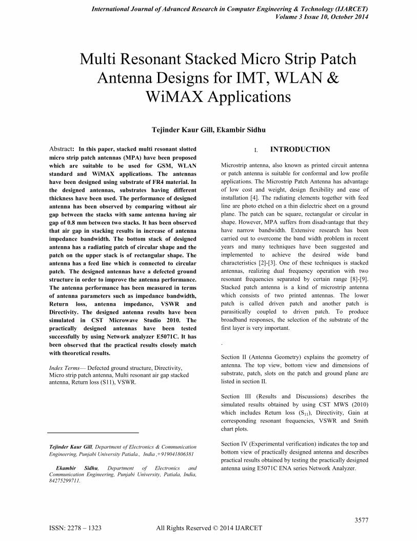
NOTE: The dotted lines in Fig. 3 represent the projection
of patch and feedline on ground. NOTE: The air gap of 0.8mm has been maintained by
inserting a 0.8 mm FR4 sheet between the two stacks at
their edges. This can be cleared from the Fig. 9 (c)
Fig. 1Top View of bottom stack of antenna
TABLE 1. ANTENNA PARAMETERS
Antenna Parameter Specification
Length of substrate (Ls) 60mm
Width of substrate (Ws) 60 mm
Radius of lower patch (R1) 18.8mm
Radius of circular slot (R2) 10.8mm
Length of feed (Lp) 112mm
Width of feed (Wp) 5.6mm
Length (L1) 22mm
Length (L2) 21mm
Length (L3) 20mm
Width (W1) 13.2mm
Width (W2) 5.6mm
Width (W3) 4mm
Width (W4) 2mm
Width (W5) 2mm
Width (W6) 2mm
Length of upper substrate (LUs) 60mm
Width of upper substrate (WUs) 60mm
Length of upper patch (LU1) 25mm
Width of upper patch (WU1) 11.6mm
Length of ground (Lg1) 12mm
Width of ground (Wg4) 60mm
Length of slot on ground (Lg5) 3mm
Width of slot on ground (Wg5) 6.4mm
Length (LU2) 30mm
Width (WU1) 24.2mm
Thickness of upper stack ( T1) 0.8mm
Thickness of lower stack ( T2) 1.57mm
Air gap (Ag) 0.8mm
Fig. 2Top view of stacked antenna
International Journal of Advanced Research in Computer Engineering & Technology (IJARCET)
Volume 3 Issue 10, October 2014
3579
ISSN: 2278 – 1323 All Rights Reserved © 2014 IJARCET
Fig. 3Bottom View of stacked antenna
Fig. 4 View of stacked antenna with air gap
III. RESULTS AND DISCUSSIONS
The designed stacked antenna have been simulated using CST Microwave Studio 2010 and the performance of the antenna has been analyzed in terms of return loss, VSWR, radiation pattern, directivity, impedance and gain. The experimental results have been also obtained using E5071C ENA series Network Analyzer and it
has been concluded that the practical results closely matches with the simulated theoretical results. Fig. 5 represents the simulated results of return loss (S11) for designed stacked antenna without
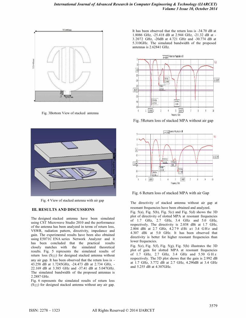
any air gap. It has been observed that the return loss is -43.258 dB at 1.7245GHz, -24.473 dB at 2.734 GHz, -22.169 dB at 3.385 GHz and -37.41 dB at 5.047GHz. The simulated bandwidth of the proposed antennas is 2.2887 GHz.
Fig. 6 represents the simulated results of return loss (S11) for designed stacked antenna without any air gap.
It has been observed that the return loss is -34.70 dB at 1.8086 GHz, -25.418 dB at 2.944 GHz, -21.32 dB at -3.2072 GHz, -20dB at 4.721 GHz and -30.774 dB at 5.310GHz. The simulated bandwidth of the proposed antennas is 2.62841 GHz.
Fig. 5Return loss of stacked MPA without air gap
Fig. 6 Return loss of stacked MPA with air Gap
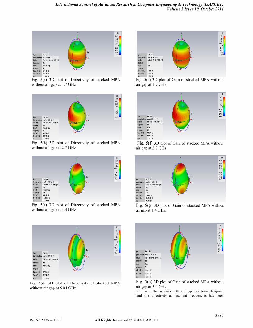
The directivity of stacked antenna without air gap at
resonant frequencies have been obtained and analyzed. Fig. 5(a), Fig. 5(b), Fig. 5(c) and Fig. 5(d) shows the 3D
plot of directivity of slotted MPA at resonant frequencies
of 1.7 GHz, 2.7 GHz, 3.4 GHz and 5.0 GHz,
respectively. The directivity is 2.038 dBi at 1.7 GHz,
2.804 dBi at 2.7 GHz, 4. 2 7 9 d Bi a t 3. 4 G H z and
4.307 dBi at 5.0 GHz. It has been observed that
directivity is better for higher resonant frequencies than
lower frequencies.
Fig. 5(e), Fig. 5(f), Fig. 5(g), Fig. 5(h) illustrates the 3D
plot of gain for slotted MPA at resonant frequencies
of 1.7 GHz, 2.7 GHz, 3.4 GHz and 5.50 G H z
respectively. The 3D plot shows that the gain is 2.992 dB
at 1.7 GHz, 3.772 dB at 2.7 GHz, 4.290dB at 3.4 GHz
and 5.255 dB at 4.307GHz.
International Journal of Advanced Research in Computer Engineering & Technology (IJARCET)
Volume 3 Issue 10, October 2014
3580
ISSN: 2278 – 1323 All Rights Reserved © 2014 IJARCET
Fig. 5(a) 3D plot of Directivity of stacked MPA
without air gap at 1.7 GHz
Fig. 5(b) 3D plot of Directivity of stacked MPA
without air gap at 2.7 GHz
Fig. 5(c) 3D plot of Directivity of stacked MPA
without air gap at 3.4 GHz
Fig. 5(d) 3D plot of Directivity of stacked MPA
without air gap at 5.04 GHz.
Fig. 5(e) 3D plot of Gain of stacked MPA without
air gap at 1.7 GHz
Fig. 5(f) 3D plot of Gain of stacked MPA without
air gap at 2.7 GHz
Fig. 5(g) 3D plot of Gain of stacked MPA without
air gap at 3.4 GHz
Fig. 5(h) 3D plot of Gain of stacked MPA without
air gap at 5.0 GHz Similarly, the antenna with air gap has been designed
and the directivity at resonant frequencies has been
International Journal of Advanced Research in Computer Engineering & Technology (IJARCET)
Volume 3 Issue 10, October 2014
3581
ISSN: 2278 – 1323 All Rights Reserved © 2014 IJARCET
obtained and analyzed. Fig. 6 (a), Fig. 6(b), Fig. 6(c),
Fig. 6(d), and Fig. 6(e) shows the 3D plot of
directivity of slotted MPA at resonant frequencies of
1.8 GHz, 2.9 GHz, 3.2 GHz, 4.7 GHz and 5.3GHz
respectively. The directivity is 2.110 dBi at 1.8 GHz,
2.139 dBi at 2.9 GHz, 4. 1 3 0 d Bi a t 3 . 2 G H z, 3.710 dBi at 4.7 GHz and 4.064 dBi at 5.3 GHz.
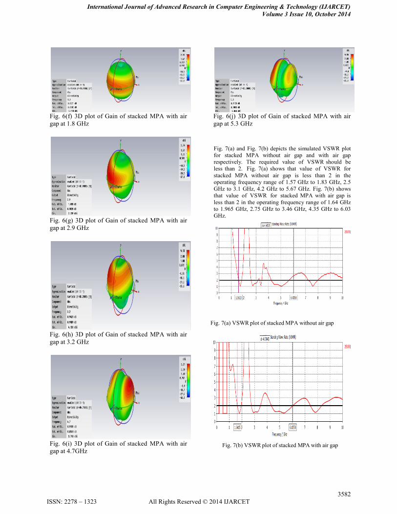
Fig. 6(f), Fig. 6(g), Fig. 6(h), Fig. 6(i) and Fig 6(j)
illustrates the 3D plot of gain for slotted MPA w i t h
a i r g a p at resonant frequencies 1.8 GHz, 2.9 GHz,
3.2 GHz, 4.7 GHz and 5.3 GHz respectively. The 3D
plot shows that the gain is 2.832 dB at 1.8 GHz, 3.748
dB at 2.9 GHz, 5.073 dB at 3.2 GHz, 4.612 dB at 4.7
GHz and 4.977 dB at 5.3 GHz
Fig. 6(a) 3D plot of Directivity of stacked MPA with
air gap at 1.8 GHz
Fig. 6(b) 3D plot of Directivity of stacked MPA with
air gap at 2.9 GHz
Fig. 6(c) 3D plot of Directivity of stacked MPA with
air gap at 3.2 GHz
Fig. 6(d) 3D plot of Directivity of stacked MPA
with air gap at 4.7 GHz
Fig. 6(e) 3D plot of Directivity of stacked MPA
with air gap at 5.3 GHz
International Journal of Advanced Research in Computer Engineering & Technology (IJARCET)
Volume 3 Issue 10, October 2014
3582
ISSN: 2278 – 1323 All Rights Reserved © 2014 IJARCET
Fig. 6(f) 3D plot of Gain of stacked MPA with air
gap at 1.8 GHz
Fig. 6(g) 3D plot of Gain of stacked MPA with air
gap at 2.9 GHz
Fig. 6(h) 3D plot of Gain of stacked MPA with air
gap at 3.2 GHz
Fig. 6(i) 3D plot of Gain of stacked MPA with air
gap at 4.7GHz
Fig. 6(j) 3D plot of Gain of stacked MPA with air
gap at 5.3 GHz
Fig. 7(a) and Fig. 7(b) depicts the simulated VSWR plot
for stacked MPA without air gap and with air gap
respectively. The required value of VSWR should be
less than 2. Fig. 7(a) shows that value of VSWR for
stacked MPA without air gap is less than 2 in the
operating frequency range of 1.57 GHz to 1.83 GHz, 2.5
GHz to 3.1 GHz, 4.2 GHz to 5.67 GHz. Fig. 7(b) shows
that value of VSWR for stacked MPA with air gap is
less than 2 in the operating frequency range of 1.64 GHz
to 1.965 GHz, 2.75 GHz to 3.46 GHz, 4.35 GHz to 6.03
GHz.
Fig. 7(a) VSWR plot of stacked MPA without air gap
Fig. 7(b) VSWR plot of stacked MPA with air gap
International Journal of Advanced Research in Computer Engineering & Technology (IJARCET)
Volume 3 Issue 10, October 2014
3583
ISSN: 2278 – 1323 All Rights Reserved © 2014 IJARCET
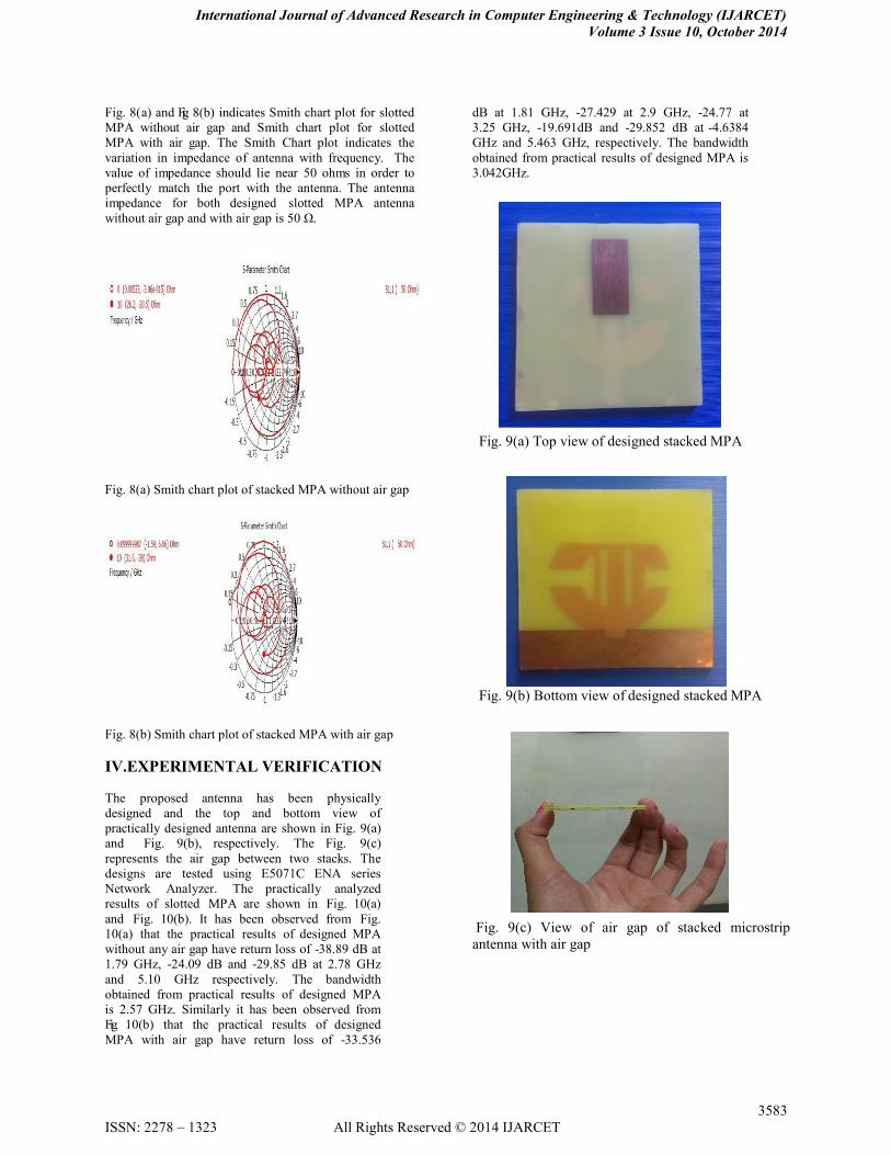
Fig. 8(a) and Fig. 8(b) indicates Smith chart plot for slotted
MPA without air gap and Smith chart plot for slotted
MPA with air gap. The Smith Chart plot indicates the
variation in impedance of antenna with frequency. The
value of impedance should lie near 50 ohms in order to
perfectly match the port with the antenna. The antenna
impedance for both designed slotted MPA antenna
without air gap and with air gap is 50 Ω.
Fig. 8(a) Smith chart plot of stacked MPA without air gap
Fig. 8(b) Smith chart plot of stacked MPA with air gap
IV.EXPERIMENTAL VERIFICATION
The proposed antenna has been physically
designed and the top and bottom view of
practically designed antenna are shown in Fig. 9(a)
and Fig. 9(b), respectively. The Fig. 9(c)
represents the air gap between two stacks. The
designs are tested using E5071C ENA series
Network Analyzer. The practically analyzed
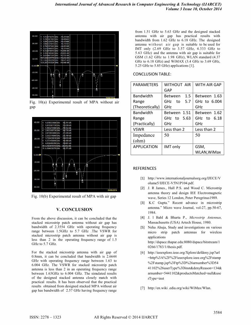
results of slotted MPA are shown in Fig. 10(a)
and Fig. 10(b). It has been observed from Fig.
10(a) that the practical results of designed MPA
without any air gap have return loss of -38.89 dB at
1.79 GHz, -24.09 dB and -29.85 dB at 2.78 GHz
and 5.10 GHz respectively. The bandwidth
obtained from practical results of designed MPA
is 2.57 GHz. Similarly it has been observed from
Fig. 10(b) that the practical results of designed
MPA with air gap have return loss of -33.536
dB at 1.81 GHz, -27.429 at 2.9 GHz, -24.77 at
3.25 GHz, -19.691dB and -29.852 dB at -4.6384
GHz and 5.463 GHz, respectively. The bandwidth
obtained from practical results of designed MPA is
3.042GHz.
Fig. 9(a) Top view of designed stacked MPA
Fig. 9(b) Bottom view of designed stacked MPA
Fig. 9(c) View of air gap of stacked microstrip
antenna with air gap
International Journal of Advanced Research in Computer Engineering & Technology (IJARCET)
Volume 3 Issue 10, October 2014
3584
ISSN: 2278 – 1323 All Rights Reserved © 2014 IJARCET
Fig. 10(a) Experimental result of MPA without air
gap
Fig. 10(b) Experimental result of MPA with air gap
V. CONCLUSION
From the above discussion, it can be concluded that the
stacked microstrip patch antenna without air gap has
bandwidth of 2.3554 GHz with operating frequency
range between 1.5GHz to 5.7 GHz .The VSWR for
stacked microstrip patch antenna without air gap is
less than 2 in the operating frequency range of 1.5
GHz to 5.7 GHz.
For the stacked microstrip antenna with air gap of
0.8mm, it can be concluded that bandwidth is 2.6644
GHz with operating frequency range between 1.63 to
6.004 GHz. The VSWR for stacked microstrip patch
antenna is less than 2 in an operating frequency range
between 1.63GHz to 6.004 GHz. The simulated results
of the designed stacked antenna closely match with
practical results. It has been observed that the practical
results obtained from designed stacked MPA without air
gap has bandwidth of 2.57 GHz having frequency range
from 1.51 GHz to 5.63 GHz and the designed stacked
antenna with air gap has practical results with
bandwidth from 1.62 GHz to 6.18 GHz. The designed
antenna w i t h o u t a i r g a p is suitable to be used for
IMT only (2.69 GHz to 3.57 GHz, 4.333 GHz to
5.63 GHz) and the antenna with air gap is suitable for
GSM (1.62 GHz to 1.98 GHz), WLAN standard (4.37
GHz to 6.18 GHz) and WiMAX (3.4 GHz to 3.69 GHz,
5.25 GHz to 5.85 GHz) applications [1].
CONCLUSION TABLE:
PARAMETERS WITHOUT AIR GAP
WITH AIR GAP
Bandwidth Range (Theoretically)
Between 1.5 GHz to 5.7 GHz
Between 1.63 GHz to 6.004 GHz
Bandwidth Range (Practically)
Between 1.51 GHz to 5.63 GHz
Between 1.62 GHz to 6.18 GHz
VSWR Less than 2 Less than 2
Impedance
(ohm)
50 50
APPLICATION IMT only GSM, WLAN,WiMax
REFERENCES
[1] http://www.internationaljournalssrg.org/IJECE/V
olume5/IJECE-V5N1P104.pdf.
[2] J. R James., Hall P.S. and Wood C. Microstrip
antenna theory and design IEE Electromagnetic
wave, Series 12 London, Peter Peregrinus1989.
[3] K.C Gupta.” Recent advance in microstrip
antenna.” Micro wave Journal, vol-27, pp.50-67,
1984.
[4] J. l BahI & Bharta P., Microstrip Antennas,
Massachusetts (USA) Artech House, 1980.
[5] Neha Ahuja, Study and investigations on various
micro strip patch antennas for wireless
applications
http://dspace.thapar.edu:8080/dspace/bitstream/1
0266/1783/1/thesis.pdf.
[6] http://ieeexplore.ieee.org/Xplore/defdeny.jsp?url
=http%3A%2F%2Fieeexplore.ieee.org%2Fstamp
%2Fstamp.jsp%3Ftp%3D%26arnumber%3D54
41102%26userType%3Dinst&denyReason=134&
arnumber=5441102&productsMatched=null&use
rType=inst
[7] http://en.wiki .edia.org/wiki/WiMax/Wlan.
International Journal of Advanced Research in Computer Engineering & Technology (IJARCET)
Volume 3 Issue 10, October 2014
3585
ISSN: 2278 – 1323 All Rights Reserved © 2014 IJARCET
[8] S.A Long & Walton M.D, A Dual-frequency
circular-disc antenna, IEEE Trans. Antenna &
Propag (USA), AP-27, and pp.270-273, 1979.
[9] T.M Au and K M Luk, Effect of
parasitic element on the characteristics
of microstrip antenna, IEEE Trans
Antenna & Propagation (USA)
39,pp.1247-1251, 1991.
[10] http://www.ursi.org/proceedings/procGA11/ursi/
AB2-4.pdf.
[11] http://en.wikipedia.org/wiki/GSM_frequency_ban
ds.