Embed Size (px)
Citation preview
© Freescale Semiconductor, Inc., 2001–2007. All rights reserved.
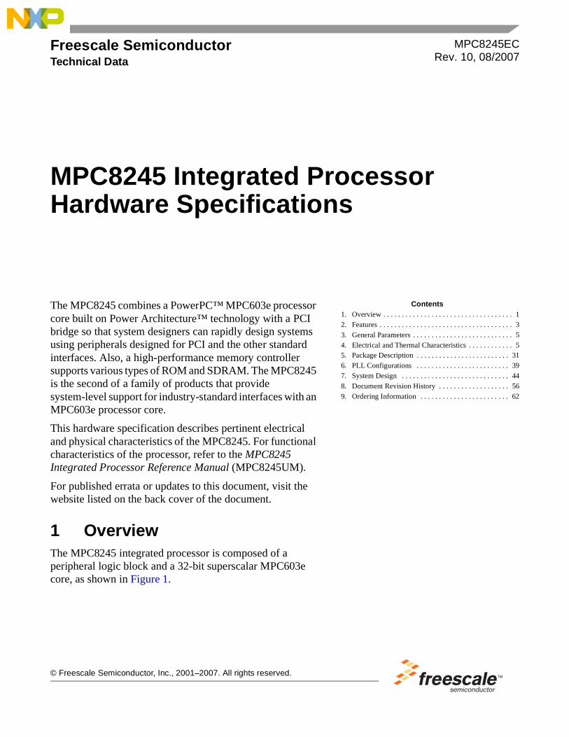
Freescale SemiconductorTechnical Data
The MPC8245 combines a PowerPC™ MPC603e processor core built on Power Architecture™ technology with a PCI bridge so that system designers can rapidly design systems using peripherals designed for PCI and the other standard interfaces. Also, a high-performance memory controller supports various types of ROM and SDRAM. The MPC8245 is the second of a family of products that provide system-level support for industry-standard interfaces with an MPC603e processor core.
This hardware specification describes pertinent electrical and physical characteristics of the MPC8245. For functional characteristics of the processor, refer to the MPC8245 Integrated Processor Reference Manual (MPC8245UM).
For published errata or updates to this document, visit the website listed on the back cover of the document.
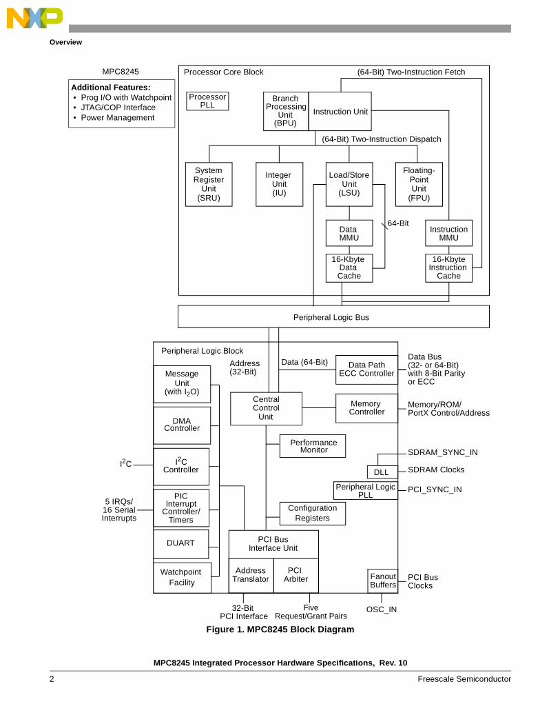
1 OverviewThe MPC8245 integrated processor is composed of a peripheral logic block and a 32-bit superscalar MPC603e core, as shown in Figure 1.
MPC8245ECRev. 10, 08/2007
Contents1. Overview . . . . . . . . . . . . . . . . . . . . . . . . . . . . . . . . . . . 12. Features . . . . . . . . . . . . . . . . . . . . . . . . . . . . . . . . . . . . 33. General Parameters . . . . . . . . . . . . . . . . . . . . . . . . . . . 54. Electrical and Thermal Characteristics . . . . . . . . . . . . 55. Package Description . . . . . . . . . . . . . . . . . . . . . . . . . 316. PLL Configurations . . . . . . . . . . . . . . . . . . . . . . . . . 397. System Design . . . . . . . . . . . . . . . . . . . . . . . . . . . . . 448. Document Revision History . . . . . . . . . . . . . . . . . . . 569. Ordering Information . . . . . . . . . . . . . . . . . . . . . . . . 62
MPC8245 Integrated Processor Hardware Specifications
MPC8245 Integrated Processor Hardware Specifications, Rev. 10
2 Freescale Semiconductor
Overview
Figure 1. MPC8245 Block Diagram
Peripheral Logic Bus
Instruction Unit
System Integer Load/Store Floating-
Data Instruction
16-Kbyte 16-Kbyte
Processor Core Block
ProcessorPLL
(64-Bit) Two-Instruction Fetch
(64-Bit) Two-Instruction Dispatch
64-Bit
Branch Processing
Unit(BPU)
MPC8245
RegisterUnit
(SRU)
Unit(IU)
Unit(LSU)
PointUnit
(FPU)
Data Cache
Instruction Cache
MMUMMU
Additional Features: • Prog I/O with Watchpoint • JTAG/COP Interface • Power Management
AddressTranslator
DLL
FanoutBuffers
PCI Arbiter
MessageUnit
(with I2O)
I2CController
DMAController
InterruptController/
PIC
Timers
PCI BusInterface Unit
Memory Controller
Data PathECC Controller
CentralControl
Unit
32-Bit OSC_INFiveRequest/Grant Pairs
I2C
5 IRQs/
Peripheral Logic Block
Peripheral LogicPLL
PCI Bus
Data (64-Bit) AddressData Bus (32- or 64-Bit)
Memory/ROM/PortX Control/Address
PCI Interface
Clocks
16 SerialInterrupts
ConfigurationRegisters
(32-Bit) with 8-Bit Parity or ECC
PCI_SYNC_IN
SDRAM_SYNC_IN
Watchpoint Facility
DUART
PerformanceMonitor
SDRAM Clocks
MPC8245 Integrated Processor Hardware Specifications, Rev. 10
Freescale Semiconductor 3
Features
The peripheral logic integrates a PCI bridge, dual universal asynchronous receiver/transmitter (DUART), memory controller, DMA controller, PIC interrupt controller, a message unit (and I2O interface), and an I2C controller. The processor core is a full-featured, high-performance processor with floating-point support, memory management, a 16-Kbyte instruction cache, a 16-Kbyte data cache, and power management features. The integration reduces the overall packaging requirements and the number of discrete devices required for an embedded system.
An internal peripheral logic bus interfaces the processor core to the peripheral logic. The core can operate at a variety of frequencies, allowing the designer to trade off performance for power consumption. The processor core is clocked from a separate PLL that is referenced to the peripheral logic PLL. This allows the microprocessor and the peripheral logic block to operate at different frequencies while maintaining a synchronous bus interface. The interface uses a 64- or 32-bit data bus (depending on memory data bus width) and a 32-bit address bus along with control signals that enable the interface between the processor and peripheral logic to be optimized for performance. PCI accesses to the MPC8245 memory space are passed to the processor bus for snooping when snoop mode is enabled.
The general-purpose processor core and peripheral logic serve a variety of embedded applications. The MPC8245 can be used as either a PCI host or PCI agent controller.
2 FeaturesMajor features of the MPC8245 are as follows:
• Processor core
— High-performance, superscalar processor core
— Integer unit (IU), floating-point unit (FPU) (software enabled or disabled), load/store unit (LSU), system register unit (SRU), and branch processing unit (BPU)
— 16-Kbyte instruction cache
— 16-Kbyte data cache
— Lockable L1 caches—Entire cache or on a per-way basis up to three of four ways
— Dynamic power management: 60x nap, doze, and sleep modes
• Peripheral logic
— Peripheral logic bus
– Various operating frequencies and bus divider ratios
– 32-bit address bus, 64-bit data bus
– Full memory coherency
– Decoupled address and data buses for pipelining of peripheral logic bus accesses
– Store gathering on peripheral logic bus-to-PCI writes
— Memory interface
– Up to 2 Gbytes of SDRAM memory
– High-bandwidth data bus (32- or 64-bit) to SDRAM
– Programmable timing supporting SDRAM
– One to eight banks of 16-, 64-, 128-, 256-, or 512-Mbit memory devices
MPC8245 Integrated Processor Hardware Specifications, Rev. 10
4 Freescale Semiconductor
Features
– Write buffering for PCI and processor accesses
– Normal parity, read-modify-write (RMW), or ECC
– Data-path buffering between memory interface and processor
– Low-voltage TTL logic (LVTTL) interfaces
– 272 Mbytes of base and extended ROM/Flash/PortX space
– Base ROM space for 8-bit data path or same size as the SDRAM data path (32- or 64-bit)
– Extended ROM space for 8-, 16-, 32-bit gathering data path, 32- or 64-bit (wide) data path
– PortX: 8-, 16-, 32-, or 64-bit general-purpose I/O port using ROM controller interface with programmable address strobe timing, data ready input signal (DRDY), and 4 chip selects
— 32-bit PCI interface
– Operates up to 66 MHz
– PCI 2.2-compatible
– PCI 5.0-V tolerance
– Dual address cycle (DAC) for 64-bit PCI addressing (master only)
– Accesses to PCI memory, I/O, and configuration spaces
– Selectable big- or little-endian operation
– Store gathering of processor-to-PCI write and PCI-to-memory write accesses
– Memory prefetching of PCI read accesses
– Selectable hardware-enforced coherency
– PCI bus arbitration unit (five request/grant pairs)
– PCI agent mode capability
– Address translation with two inbound and outbound units (ATU)
– Internal configuration registers accessible from PCI
— Two-channel integrated DMA controller (writes to ROM/PortX not supported)
– Direct mode or chaining mode (automatic linking of DMA transfers)
– Scatter gathering—Read or write discontinuous memory
– 64-byte transfer queue per channel
– Interrupt on completed segment, chain, and error
– Local-to-local memory
– PCI-to-PCI memory
– Local-to-PCI memory
– PCI memory-to-local memory
— Message unit
– Two doorbell registers
– Two inbound and two outbound messaging registers
– I2O message interface
— I2C controller with full master/slave support that accepts broadcast messages
MPC8245 Integrated Processor Hardware Specifications, Rev. 10
Freescale Semiconductor 5
General Parameters
— Programmable interrupt controller (PIC)
– Five hardware interrupts (IRQs) or 16 serial interrupts
– Four programmable timers with cascade
— Two (dual) universal asynchronous receiver/transmitters (UARTs)
— Integrated PCI bus and SDRAM clock generation
— Programmable PCI bus and memory interface output drivers
• System-level performance monitor facility
• Debug features
— Memory attribute and PCI attribute signals
— Debug address signals
— MIV signal—Marks valid address and data bus cycles on the memory bus
— Programmable input and output signals with watchpoint capability
— Error injection/capture on data path
— IEEE Std 1149.1® (JTAG)/test interface
3 General ParametersThe following list summarizes the general parameters of the MPC8245:
Technology 0.25-µm CMOS, five-layer metal
Die size 49.2 mm2
Transistor count 4.5 million
Logic design Fully-static
Packages Surface-mount 352 tape ball grid array (TBGA)
Core power supply 1.7 V to 2.1 V DC for 266 and 300 MHz with the condition that the usage is “nominal” ± 100 mV where “nominal” is 1.8/1.9/2.0 volts.
1.9 V to 2.2 V DC for 333 and 350 MHz with the condition that the usage is “nominal” ± 100 mV where “nominal” is 2.0/2.1 volts.
See Table 2 for details of recommended operating conditions)
I/O power supply 3.0- to 3.6-V DC
4 Electrical and Thermal CharacteristicsThis section provides the AC and DC electrical specifications and thermal characteristics for the MPC8245.
4.1 DC Electrical CharacteristicsThis section covers ratings, conditions, and other DC electrical characteristics.
MPC8245 Integrated Processor Hardware Specifications, Rev. 10
6 Freescale Semiconductor
Electrical and Thermal Characteristics
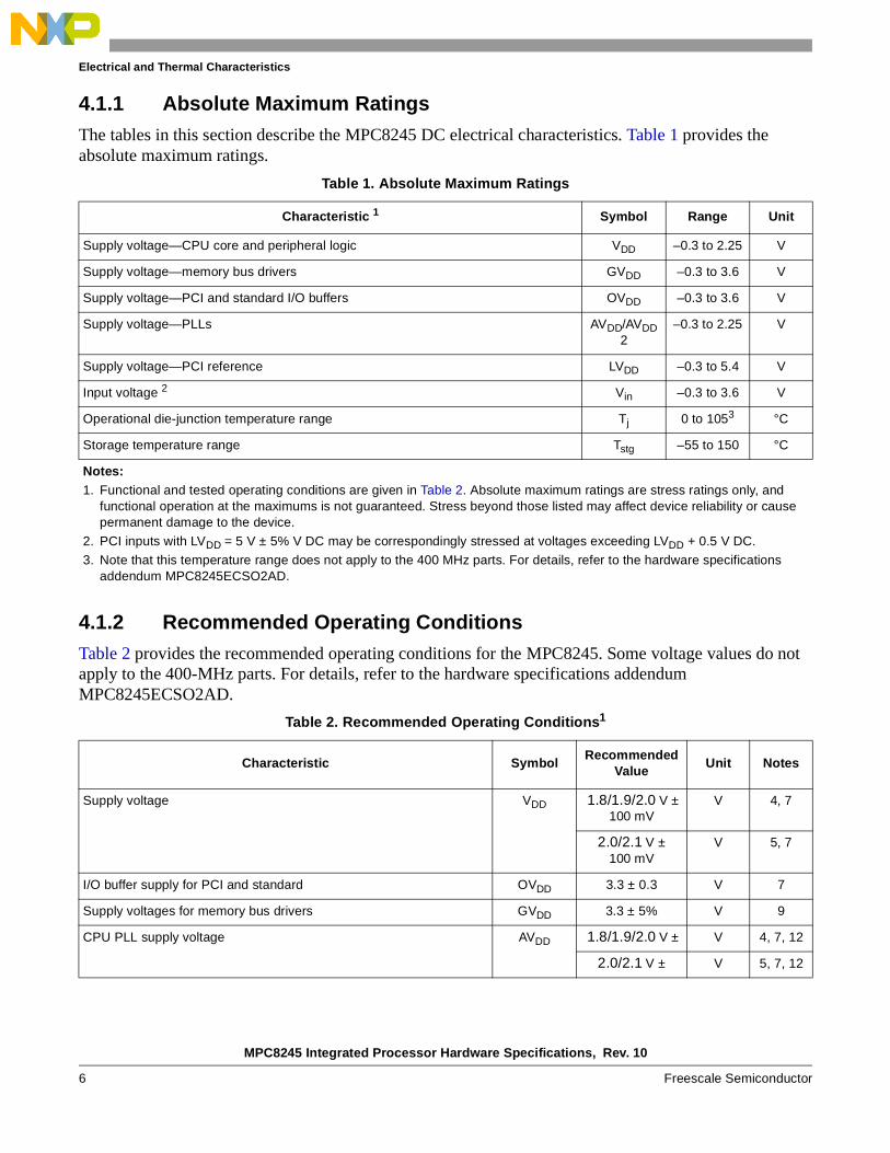
4.1.1 Absolute Maximum RatingsThe tables in this section describe the MPC8245 DC electrical characteristics. Table 1 provides the absolute maximum ratings.
4.1.2 Recommended Operating ConditionsTable 2 provides the recommended operating conditions for the MPC8245. Some voltage values do not apply to the 400-MHz parts. For details, refer to the hardware specifications addendum MPC8245ECSO2AD.
Table 1. Absolute Maximum Ratings
Characteristic 1 Symbol Range Unit
Supply voltage—CPU core and peripheral logic VDD –0.3 to 2.25 V
Supply voltage—memory bus drivers GVDD –0.3 to 3.6 V
Supply voltage—PCI and standard I/O buffers OVDD –0.3 to 3.6 V
Supply voltage—PLLs AVDD/AVDD2
–0.3 to 2.25 V
Supply voltage—PCI reference LVDD –0.3 to 5.4 V
Input voltage 2 Vin –0.3 to 3.6 V
Operational die-junction temperature range Tj 0 to 1053 °C
Storage temperature range Tstg –55 to 150 °C
Notes:1. Functional and tested operating conditions are given in Table 2. Absolute maximum ratings are stress ratings only, and
functional operation at the maximums is not guaranteed. Stress beyond those listed may affect device reliability or cause permanent damage to the device.
2. PCI inputs with LVDD = 5 V ± 5% V DC may be correspondingly stressed at voltages exceeding LVDD + 0.5 V DC.
3. Note that this temperature range does not apply to the 400 MHz parts. For details, refer to the hardware specifications addendum MPC8245ECSO2AD.
Table 2. Recommended Operating Conditions1
Characteristic SymbolRecommended
ValueUnit Notes
Supply voltage VDD 1.8/1.9/2.0 V ± 100 mV
V 4, 7
2.0/2.1 V ± 100 mV
V 5, 7
I/O buffer supply for PCI and standard OVDD 3.3 ± 0.3 V 7
Supply voltages for memory bus drivers GVDD 3.3 ± 5% V 9
CPU PLL supply voltage AVDD 1.8/1.9/2.0 V ± V 4, 7, 12
2.0/2.1 V ± V 5, 7, 12
MPC8245 Integrated Processor Hardware Specifications, Rev. 10
Freescale Semiconductor 7
Electrical and Thermal Characteristics
PLL supply voltage—peripheral logic AVDD2 1.8/1.9/2.0 V ± V 4, 7, 12
2.0/2.1 V ± V 5, 7, 12
PCI reference LVDD 5.0 ± 5% V 2, 10, 11
3.3 ± 0.3 V 3, 10, 11
Input voltage PCI inputs Vin 0 to 3.6 or 5.75 V 2, 3
All other inputs 0 to 3.6 V 6
Die-junction temperature Tj 0 to 105 °C
Notes: 1. These are the recommended and tested operating conditions. Proper device operation outside of these conditions is not
guaranteed.
2. PCI pins are designed to withstand LVDD + 5% V DC when LVDD is connected to a 5.0-V DC power supply.
3. PCI pins are designed to withstand LVDD + 0.5 V DC when LVDD is connected to a 3.3-V DC power supply.
4. The voltage supply value of 1.8/1.9/2.0 V ± 100 mV applies to parts marked as having a maximum CPU speed of 266 and 300 MHz. See Table 7. For each chosen nominal value (1.8/1.9/2.0 V) the supply voltage should not exceed ± 100 mV of the nominal value.
5. The voltage supply value of 2.0/2.1 V ± 100 m V applies to parts marked as having a maximum CPU speed of 333 and 350 MHz. See Table 7. For each chosen nominal value (2.0/2.1 V) the supply voltage should not exceed ± 100 mV of the nominal value.
Cautions:6. Input voltage (Vin) must not be greater than the supply voltage (VDD/AVDD/AVDD2) by more than 2.5 V at all times, including
during power-on reset. Input voltage (Vin) must not be greater than GVDD/OVDD by more than 0.6 V at all times, including during power-on reset.
7. OVDD must not exceed VDD/AVDD/AVDD2 by more than 1.8 V at any time, including during power-on reset. This limit may be exceeded for a maximum of 20 ms during power-on reset and power-down sequences.
8. VDD/AVDD/AVDD2 must not exceed OVDD by more than 0.6 V at any time, including during power-on reset. This limit may be exceeded for a maximum of 20 ms during power-on reset and power-down sequences.
9. GVDD must not exceed VDD/AVDD/AVDD2 by more than 1.8 V at any time, including during power-on reset. This limit may be exceeded for a maximum of 20 ms during power-on reset and power-down sequences.
10.LVDD must not exceed VDD/AVDD/AVDD2 by more than 5.4 V at any time, including during power-on reset. This limit may be exceeded for a maximum of 20 ms during power-on reset and power-down sequences.
11.LVDD must not exceed OVDD by more than 3.0 V at any time, including during power-on reset. This limit may be exceeded for a maximum of 20 ms during power-on reset and power-down sequences.
12.This voltage is the input to the filter discussed in Section 7.1, “PLL Power Supply Filtering,” and not necessarily the voltage at the AVDD pin, which may be reduced from VDD by the filter.
Table 2. Recommended Operating Conditions1 (continued)
Characteristic SymbolRecommended
ValueUnit Notes
MPC8245 Integrated Processor Hardware Specifications, Rev. 10
8 Freescale Semiconductor
Electrical and Thermal Characteristics
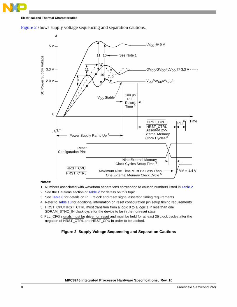
Figure 2 shows supply voltage sequencing and separation cautions.
Figure 2. Supply Voltage Sequencing and Separation Cautions
OVDD/GVDD/(LVDD @ 3.3 V - - - -)
VDD/AVDD/AVDD2
LVDD @ 5 V
Time
3.3 V
5 V
2.0 V
0
8
11
10
1011
7, 9
DC
Pow
er S
uppl
y V
olta
ge
ResetConfiguration Pins
HRST_CPU,HRST_CTRL
PLLRelockTime 3
100 µs
Nine External Memory
Asserted 255External Memory
HRST_CPU,
HRST_CTRL
VDD Stable
Power Supply Ramp Up 2
See Note 1
Clock Cycles 3
Clock Cycles Setup Time 4
VM = 1.4 VMaximum Rise Time Must Be Less ThanOne External Memory Clock Cycle 5
Notes: 1. Numbers associated with waveform separations correspond to caution numbers listed in Table 2.
2. See the Cautions section of Table 2 for details on this topic.
3. See Table 8 for details on PLL relock and reset signal assertion timing requirements.
4. Refer to Table 10 for additional information on reset configuration pin setup timing requirements.
5. HRST_CPU/HRST_CTRL must transition from a logic 0 to a logic 1 in less than one SDRAM_SYNC_IN clock cycle for the device to be in the nonreset state.
6. PLL_CFG signals must be driven on reset and must be held for at least 25 clock cycles after the negation of HRST_CTRL and HRST_CPU in order to be latched.
PLL 6
MPC8245 Integrated Processor Hardware Specifications, Rev. 10
Freescale Semiconductor 9
Electrical and Thermal Characteristics
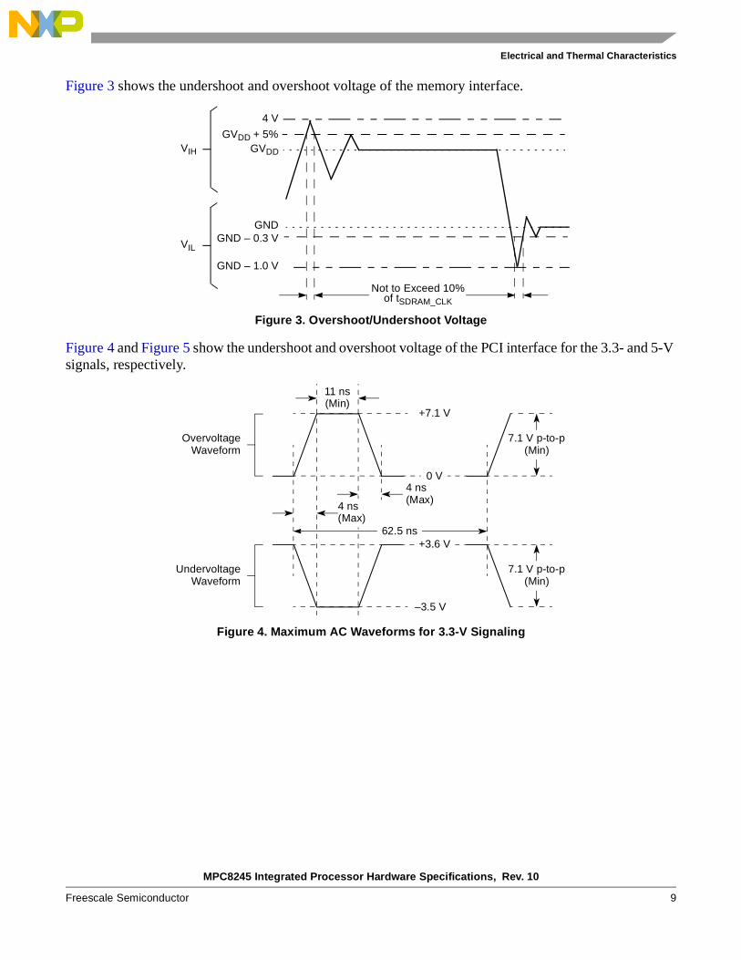
Figure 3 shows the undershoot and overshoot voltage of the memory interface.
Figure 3. Overshoot/Undershoot Voltage
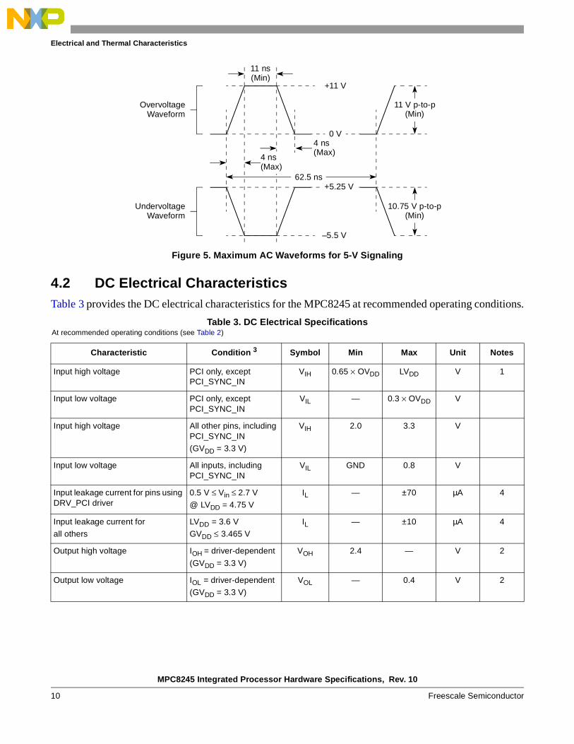
Figure 4 and Figure 5 show the undershoot and overshoot voltage of the PCI interface for the 3.3- and 5-V signals, respectively.
Figure 4. Maximum AC Waveforms for 3.3-V Signaling
GNDGND – 0.3 V
GND – 1.0 V
Not to Exceed 10%
GVDD
of tSDRAM_CLK
GVDD + 5%
4 V
VIH
VIL
UndervoltageWaveform
OvervoltageWaveform
11 ns(Min)
+7.1 V
7.1 V p-to-p(Min)
4 ns(Max)
–3.5 V
7.1 V p-to-p(Min)
62.5 ns+3.6 V
0 V
4 ns(Max)
MPC8245 Integrated Processor Hardware Specifications, Rev. 10
10 Freescale Semiconductor
Electrical and Thermal Characteristics
Figure 5. Maximum AC Waveforms for 5-V Signaling
4.2 DC Electrical CharacteristicsTable 3 provides the DC electrical characteristics for the MPC8245 at recommended operating conditions.
Table 3. DC Electrical SpecificationsAt recommended operating conditions (see Table 2)
Characteristic Condition 3 Symbol Min Max Unit Notes
Input high voltage PCI only, except PCI_SYNC_IN
VIH 0.65 × OVDD LVDD V 1
Input low voltage PCI only, except PCI_SYNC_IN
VIL — 0.3 × OVDD V
Input high voltage All other pins, including PCI_SYNC_IN
(GVDD = 3.3 V)
VIH 2.0 3.3 V
Input low voltage All inputs, including PCI_SYNC_IN
VIL GND 0.8 V
Input leakage current for pins using DRV_PCI driver
0.5 V ≤ Vin ≤ 2.7 V
@ LVDD = 4.75 V
IL — ±70 µA 4
Input leakage current for
all others
LVDD = 3.6 V
GVDD ≤ 3.465 V
IL — ±10 µA 4
Output high voltage IOH = driver-dependent
(GVDD = 3.3 V)
VOH 2.4 — V 2
Output low voltage IOL = driver-dependent
(GVDD = 3.3 V)
VOL — 0.4 V 2
UndervoltageWaveform
OvervoltageWaveform
11 ns(Min)
+11 V
11 V p-to-p(Min)
4 ns(Max)
–5.5 V
10.75 V p-to-p(Min)
62.5 ns+5.25 V
0 V
4 ns(Max)
MPC8245 Integrated Processor Hardware Specifications, Rev. 10
Freescale Semiconductor 11
Electrical and Thermal Characteristics
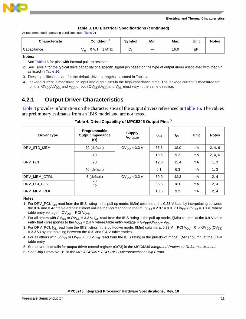
4.2.1 Output Driver CharacteristicsTable 4 provides information on the characteristics of the output drivers referenced in Table 16. The values are preliminary estimates from an IBIS model and are not tested.
Capacitance Vin = 0 V, f = 1 MHz Cin — 16.0 pF
Notes: 1. See Table 16 for pins with internal pull-up resistors.
2. See Table 4 for the typical drive capability of a specific signal pin based on the type of output driver associated with that pin as listed in Table 16.
3. These specifications are for the default driver strengths indicated in Table 4.
4. Leakage current is measured on input and output pins in the high-impedance state. The leakage current is measured for nominal OVDD/LVDD, and VDD or both OVDD/LVDD and VDD must vary in the same direction.
Table 4. Drive Capability of MPC8245 Output Pins 5
Driver TypeProgrammable
Output Impedance(Ω)
SupplyVoltage
IOH IOL Unit Notes
DRV_STD_MEM 20 (default) OVDD = 3.3 V 36.6 18.0 mA 2, 4, 6
40 18.6 9.2 mA 2, 4, 6
DRV_PCI 20 12.0 12.4 mA 1, 3
40 (default) 6.1 6.3 mA 1, 3
DRV_MEM_CTRL 6 (default)2040
GVDD = 3.3 V 89.0 42.3 mA 2, 4
DRV_PCI_CLK 36.6 18.0 mA 2, 4
DRV_MEM_CLK 18.6 9.2 mA 2, 4
Notes:1. For DRV_PCI, IOH read from the IBIS listing in the pull-up mode, I(Min) column, at the 0.33-V label by interpolating between
the 0.3- and 0.4-V table entries’ current values that correspond to the PCI VOH = 2.97 = 0.9 × OVDD (OVDD = 3.3 V) where table entry voltage = OVDD – PCI VOH.
2. For all others with GVDD or OVDD = 3.3 V, IOH read from the IBIS listing in the pull-up mode, I(Min) column, at the 0.9-V table entry that corresponds to the VOH = 2.4 V where table entry voltage = GVDD/OVDD – VOH.
3. For DRV_PCI, IOL read from the IBIS listing in the pull-down mode, I(Min) column, at 0.33 V = PCI VOL = 0 × OVDD (OVDD = 3.3 V) by interpolating between the 0.3- and 0.4-V table entries.
4. For all others with GVDD or OVDD = 3.3 V, IOL read from the IBIS listing in the pull-down mode, I(Min) column, at the 0.4-V table entry.
5. See driver bit details for output driver control register (0x73) in the MPC8245 Integrated Processor Reference Manual.
6. See Chip Errata No. 19 in the MPC8245/MPC8241 RISC Microprocessor Chip Errata.
Table 3. DC Electrical Specifications (continued)At recommended operating conditions (see Table 2)
Characteristic Condition 3 Symbol Min Max Unit Notes
MPC8245 Integrated Processor Hardware Specifications, Rev. 10
12 Freescale Semiconductor
Electrical and Thermal Characteristics
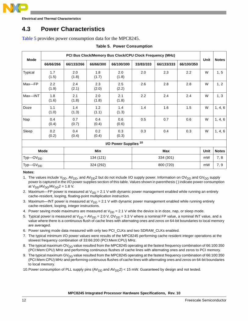
4.3 Power CharacteristicsTable 5 provides power consumption data for the MPC8245.
Table 5. Power Consumption
ModePCI Bus Clock/Memory Bus Clock/CPU Clock Frequency (MHz)
Unit Notes66/66/266 66/133/266 66/66/300 66/100/300 33/83/333 66/133/333 66/100/350
Typical 1.7(1.5)
2.0(1.8)
1.8(1.7)
2.0(1.8)
2.0 2.3 2.2 W 1, 5
Max—FP 2.2(1.9)
2.4(2.1)
2.3(2.0)
2.5(2.2)
2.6 2.8 2.8 W 1, 2
Max—INT 1.8(1.6)
2.1(1.8)
2.0(1.8)
2.1(1.8)
2.2 2.4 2.4 W 1, 3
Doze 1.1(1.0)
1.4(1.3)
1.2(1.1)
1.4(1.3)
1.4 1.6 1.5 W 1, 4, 6
Nap 0.4(0.4)
0.7(0.7)
0.4(0.4)
0.6(0.6)
0.5 0.7 0.6 W 1, 4, 6
Sleep 0.2(0.2)
0.4(0.4)
0.2(0.4)
0.3(0.3)
0.3 0.4 0.3 W 1, 4, 6
I/O Power Supplies 10
Mode Min Max Unit Notes
Typ—OVDD 134 (121) 334 (301) mW 7, 8
Typ—GVDD 324 (292) 800 (720) mW 7, 9
Notes:1. The values include VDD, AVDD, and AVDD2 but do not include I/O supply power. Information on OVDD and GVDD supply
power is captured in the I/O power supplies section of this table. Values shown in parenthesis ( ) indicate power consumption at VDD/AVDD/AVDD2 = 1.8 V.
2. Maximum—FP power is measured at VDD = 2.1 V with dynamic power management enabled while running an entirely cache-resident, looping, floating-point multiplication instruction.
3. Maximum—INT power is measured at VDD = 2.1 V with dynamic power management enabled while running entirely cache-resident, looping, integer instructions.
4. Power saving mode maximums are measured at VDD = 2.1 V while the device is in doze, nap, or sleep mode.
5. Typical power is measured at VDD = AVDD = 2.0 V, OVDD = 3.3 V where a nominal FP value, a nominal INT value, and a value where there is a continuous flush of cache lines with alternating ones and zeros on 64-bit boundaries to local memory are averaged.
6. Power saving mode data measured with only two PCI_CLKs and two SDRAM_CLKs enabled.
7. The typical minimum I/O power values were results of the MPC8245 performing cache resident integer operations at the slowest frequency combination of 33:66:200 (PCI:Mem:CPU) MHz.
8. The typical maximum OVDD value resulted from the MPC8245 operating at the fastest frequency combination of 66:100:350 (PCI:Mem:CPU) MHz and performing continuous flushes of cache lines with alternating ones and zeros to PCI memory.
9. The typical maximum GVDD value resulted from the MPC8245 operating at the fastest frequency combination of 66:100:350 (PCI:Mem:CPU) MHz and performing continuous flushes of cache lines with alternating ones and zeros on 64-bit boundaries to local memory.
10.Power consumption of PLL supply pins (AVDD and AVDD2) < 15 mW. Guaranteed by design and not tested.
MPC8245 Integrated Processor Hardware Specifications, Rev. 10
Freescale Semiconductor 13
Electrical and Thermal Characteristics
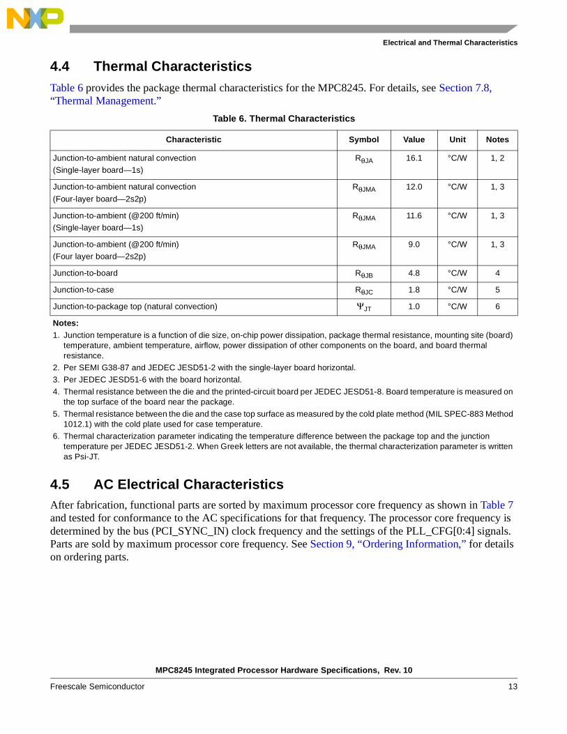
4.4 Thermal CharacteristicsTable 6 provides the package thermal characteristics for the MPC8245. For details, see Section 7.8, “Thermal Management.”
4.5 AC Electrical CharacteristicsAfter fabrication, functional parts are sorted by maximum processor core frequency as shown in Table 7 and tested for conformance to the AC specifications for that frequency. The processor core frequency is determined by the bus (PCI_SYNC_IN) clock frequency and the settings of the PLL_CFG[0:4] signals. Parts are sold by maximum processor core frequency. See Section 9, “Ordering Information,” for details on ordering parts.
Table 6. Thermal Characteristics
Characteristic Symbol Value Unit Notes
Junction-to-ambient natural convection
(Single-layer board—1s)
RθJA 16.1 °C/W 1, 2
Junction-to-ambient natural convection
(Four-layer board—2s2p)
RθJMA 12.0 °C/W 1, 3
Junction-to-ambient (@200 ft/min)
(Single-layer board—1s)
RθJMA 11.6 °C/W 1, 3
Junction-to-ambient (@200 ft/min)
(Four layer board—2s2p)
RθJMA 9.0 °C/W 1, 3
Junction-to-board RθJB 4.8 °C/W 4
Junction-to-case RθJC 1.8 °C/W 5
Junction-to-package top (natural convection) ΨJT 1.0 °C/W 6
Notes:1. Junction temperature is a function of die size, on-chip power dissipation, package thermal resistance, mounting site (board)
temperature, ambient temperature, airflow, power dissipation of other components on the board, and board thermal resistance.
2. Per SEMI G38-87 and JEDEC JESD51-2 with the single-layer board horizontal.
3. Per JEDEC JESD51-6 with the board horizontal.
4. Thermal resistance between the die and the printed-circuit board per JEDEC JESD51-8. Board temperature is measured on the top surface of the board near the package.
5. Thermal resistance between the die and the case top surface as measured by the cold plate method (MIL SPEC-883 Method 1012.1) with the cold plate used for case temperature.
6. Thermal characterization parameter indicating the temperature difference between the package top and the junction temperature per JEDEC JESD51-2. When Greek letters are not available, the thermal characterization parameter is written as Psi-JT.
MPC8245 Integrated Processor Hardware Specifications, Rev. 10
14 Freescale Semiconductor
Electrical and Thermal Characteristics
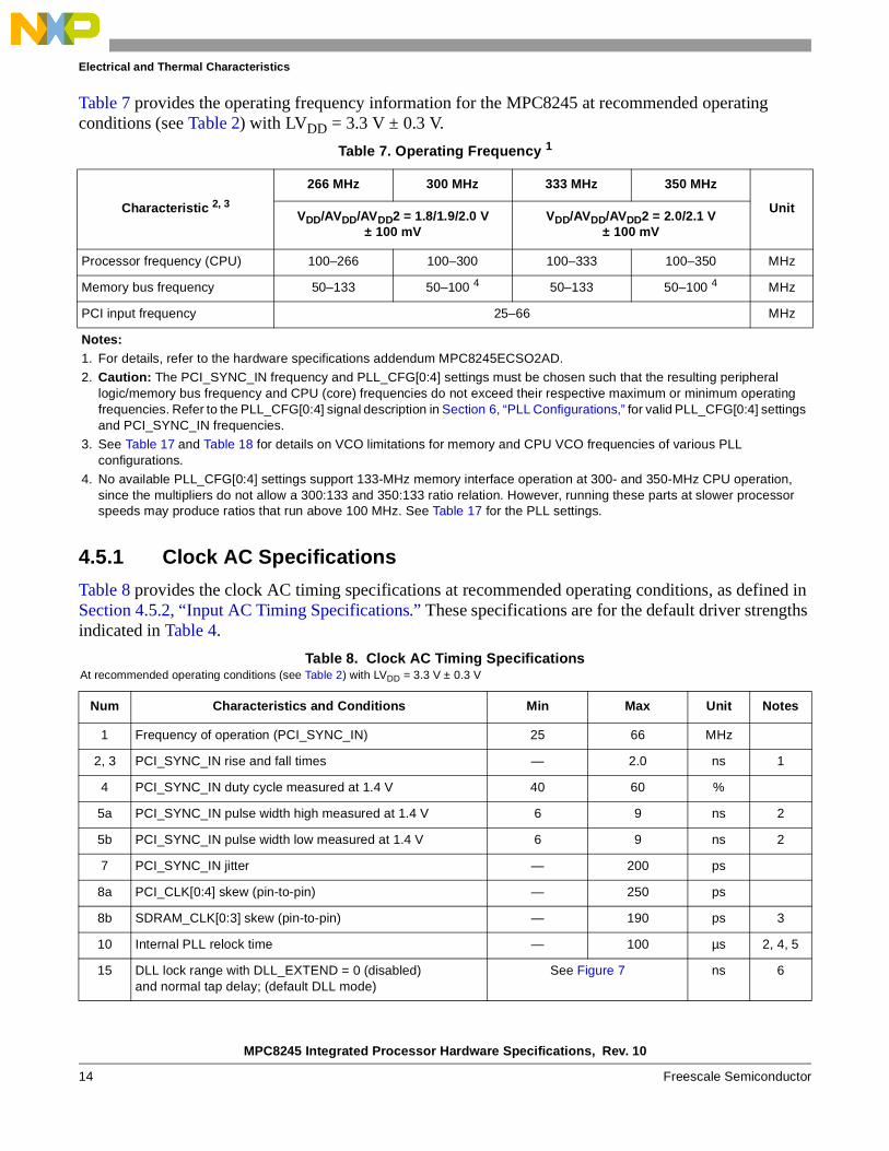
Table 7 provides the operating frequency information for the MPC8245 at recommended operating conditions (see Table 2) with LVDD = 3.3 V ± 0.3 V.
4.5.1 Clock AC Specifications
Table 8 provides the clock AC timing specifications at recommended operating conditions, as defined in Section 4.5.2, “Input AC Timing Specifications.” These specifications are for the default driver strengths indicated in Table 4.
Table 7. Operating Frequency 1
Characteristic 2, 3
266 MHz 300 MHz 333 MHz 350 MHz
UnitVDD/AVDD/AVDD2 = 1.8/1.9/2.0 V
± 100 mV VDD/AVDD/AVDD2 = 2.0/2.1 V
± 100 mV
Processor frequency (CPU) 100–266 100–300 100–333 100–350 MHz
Memory bus frequency 50–133 50–100 4 50–133 50–100 4 MHz
PCI input frequency 25–66 MHz
Notes:1. For details, refer to the hardware specifications addendum MPC8245ECSO2AD.
2. Caution: The PCI_SYNC_IN frequency and PLL_CFG[0:4] settings must be chosen such that the resulting peripheral logic/memory bus frequency and CPU (core) frequencies do not exceed their respective maximum or minimum operating frequencies. Refer to the PLL_CFG[0:4] signal description in Section 6, “PLL Configurations,” for valid PLL_CFG[0:4] settings and PCI_SYNC_IN frequencies.
3. See Table 17 and Table 18 for details on VCO limitations for memory and CPU VCO frequencies of various PLL configurations.
4. No available PLL_CFG[0:4] settings support 133-MHz memory interface operation at 300- and 350-MHz CPU operation, since the multipliers do not allow a 300:133 and 350:133 ratio relation. However, running these parts at slower processor speeds may produce ratios that run above 100 MHz. See Table 17 for the PLL settings.
Table 8. Clock AC Timing SpecificationsAt recommended operating conditions (see Table 2) with LVDD = 3.3 V ± 0.3 V
Num Characteristics and Conditions Min Max Unit Notes
1 Frequency of operation (PCI_SYNC_IN) 25 66 MHz
2, 3 PCI_SYNC_IN rise and fall times — 2.0 ns 1
4 PCI_SYNC_IN duty cycle measured at 1.4 V 40 60 %
5a PCI_SYNC_IN pulse width high measured at 1.4 V 6 9 ns 2
5b PCI_SYNC_IN pulse width low measured at 1.4 V 6 9 ns 2
7 PCI_SYNC_IN jitter — 200 ps
8a PCI_CLK[0:4] skew (pin-to-pin) — 250 ps
8b SDRAM_CLK[0:3] skew (pin-to-pin) — 190 ps 3
10 Internal PLL relock time — 100 µs 2, 4, 5
15 DLL lock range with DLL_EXTEND = 0 (disabled) and normal tap delay; (default DLL mode)
See Figure 7 ns 6
MPC8245 Integrated Processor Hardware Specifications, Rev. 10
Freescale Semiconductor 15
Electrical and Thermal Characteristics
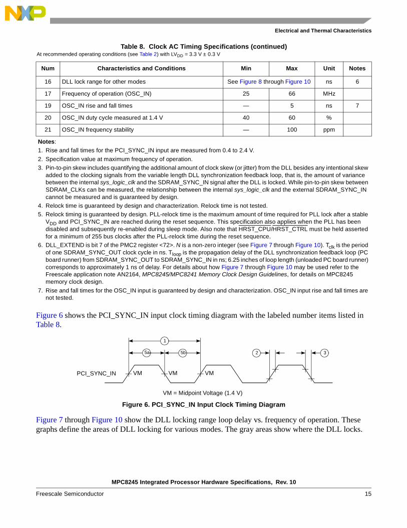
Figure 6 shows the PCI_SYNC_IN input clock timing diagram with the labeled number items listed in Table 8.
Figure 6. PCI_SYNC_IN Input Clock Timing Diagram
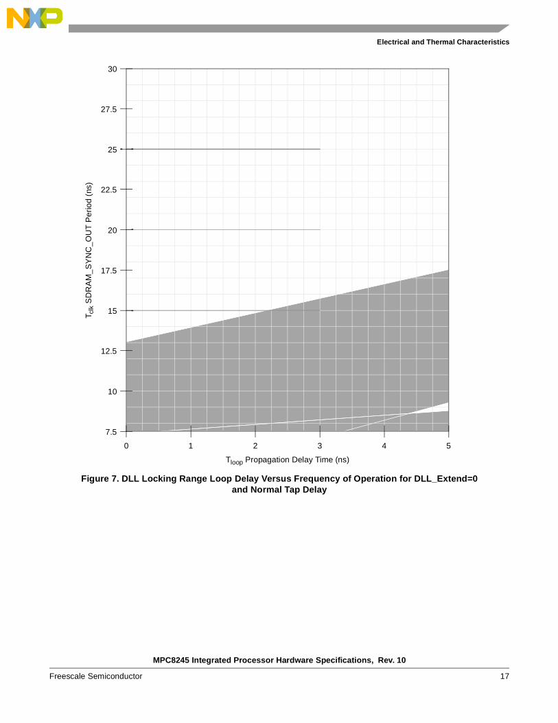
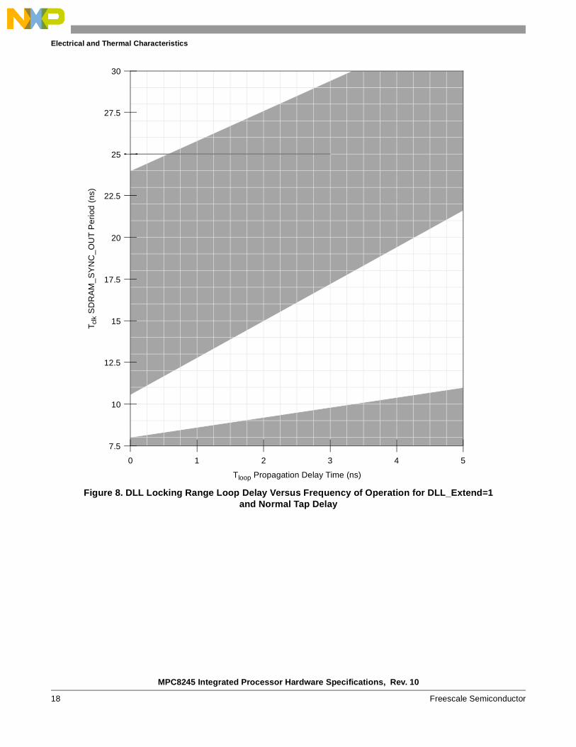
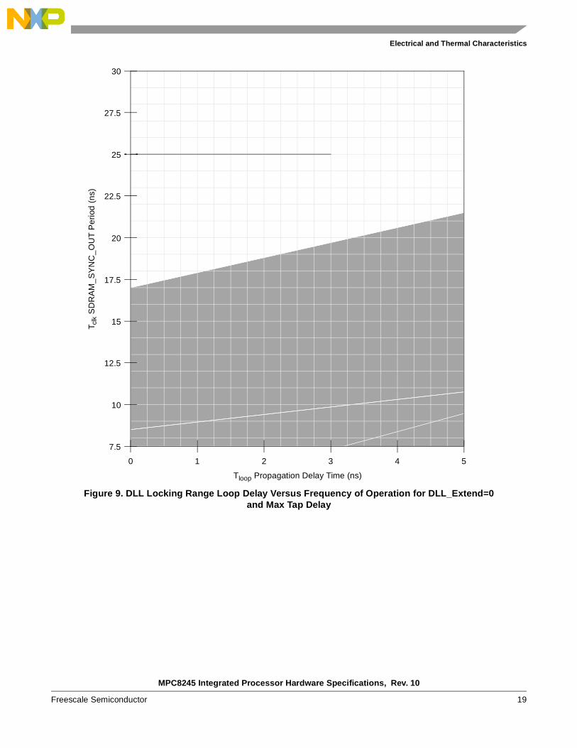
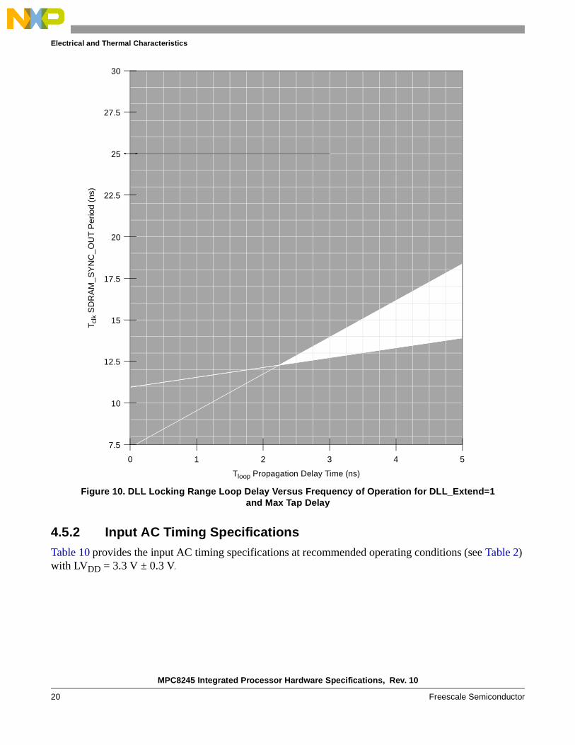
Figure 7 through Figure 10 show the DLL locking range loop delay vs. frequency of operation. These graphs define the areas of DLL locking for various modes. The gray areas show where the DLL locks.
16 DLL lock range for other modes See Figure 8 through Figure 10 ns 6
17 Frequency of operation (OSC_IN) 25 66 MHz
19 OSC_IN rise and fall times — 5 ns 7
20 OSC_IN duty cycle measured at 1.4 V 40 60 %
21 OSC_IN frequency stability — 100 ppm
Notes:
1. Rise and fall times for the PCI_SYNC_IN input are measured from 0.4 to 2.4 V.
2. Specification value at maximum frequency of operation.
3. Pin-to-pin skew includes quantifying the additional amount of clock skew (or jitter) from the DLL besides any intentional skew added to the clocking signals from the variable length DLL synchronization feedback loop, that is, the amount of variance between the internal sys_logic_clk and the SDRAM_SYNC_IN signal after the DLL is locked. While pin-to-pin skew between SDRAM_CLKs can be measured, the relationship between the internal sys_logic_clk and the external SDRAM_SYNC_IN cannot be measured and is guaranteed by design.
4. Relock time is guaranteed by design and characterization. Relock time is not tested.
5. Relock timing is guaranteed by design. PLL-relock time is the maximum amount of time required for PLL lock after a stable VDD and PCI_SYNC_IN are reached during the reset sequence. This specification also applies when the PLL has been disabled and subsequently re-enabled during sleep mode. Also note that HRST_CPU/HRST_CTRL must be held asserted for a minimum of 255 bus clocks after the PLL-relock time during the reset sequence.
6. DLL_EXTEND is bit 7 of the PMC2 register <72>. N is a non-zero integer (see Figure 7 through Figure 10). Tclk is the period of one SDRAM_SYNC_OUT clock cycle in ns. Tloop is the propagation delay of the DLL synchronization feedback loop (PC board runner) from SDRAM_SYNC_OUT to SDRAM_SYNC_IN in ns; 6.25 inches of loop length (unloaded PC board runner) corresponds to approximately 1 ns of delay. For details about how Figure 7 through Figure 10 may be used refer to the Freescale application note AN2164, MPC8245/MPC8241 Memory Clock Design Guidelines, for details on MPC8245 memory clock design.
7. Rise and fall times for the OSC_IN input is guaranteed by design and characterization. OSC_IN input rise and fall times are not tested.
Table 8. Clock AC Timing Specifications (continued)At recommended operating conditions (see Table 2) with LVDD = 3.3 V ± 0.3 V
Num Characteristics and Conditions Min Max Unit Notes
5a 5b
VM
VM = Midpoint Voltage (1.4 V)
2 3
1
PCI_SYNC_IN VM VM
MPC8245 Integrated Processor Hardware Specifications, Rev. 10
16 Freescale Semiconductor
Electrical and Thermal Characteristics
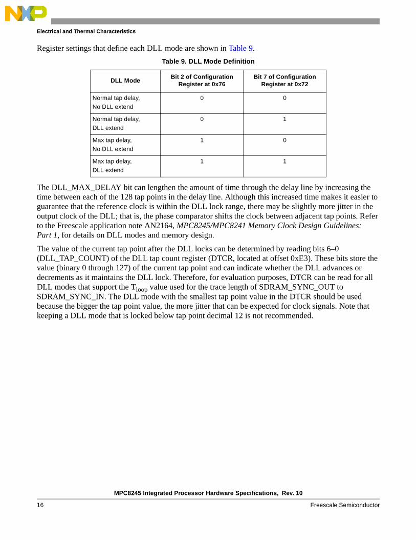
Register settings that define each DLL mode are shown in Table 9.
The DLL_MAX_DELAY bit can lengthen the amount of time through the delay line by increasing the time between each of the 128 tap points in the delay line. Although this increased time makes it easier to guarantee that the reference clock is within the DLL lock range, there may be slightly more jitter in the output clock of the DLL; that is, the phase comparator shifts the clock between adjacent tap points. Refer to the Freescale application note AN2164, MPC8245/MPC8241 Memory Clock Design Guidelines: Part 1, for details on DLL modes and memory design.
The value of the current tap point after the DLL locks can be determined by reading bits 6–0 (DLL_TAP_COUNT) of the DLL tap count register (DTCR, located at offset 0xE3). These bits store the value (binary 0 through 127) of the current tap point and can indicate whether the DLL advances or decrements as it maintains the DLL lock. Therefore, for evaluation purposes, DTCR can be read for all DLL modes that support the Tloop value used for the trace length of SDRAM_SYNC_OUT to SDRAM_SYNC_IN. The DLL mode with the smallest tap point value in the DTCR should be used because the bigger the tap point value, the more jitter that can be expected for clock signals. Note that keeping a DLL mode that is locked below tap point decimal 12 is not recommended.
Table 9. DLL Mode Definition
DLL ModeBit 2 of Configuration
Register at 0x76Bit 7 of Configuration
Register at 0x72
Normal tap delay,
No DLL extend
0 0
Normal tap delay,
DLL extend
0 1
Max tap delay,
No DLL extend
1 0
Max tap delay,
DLL extend
1 1
MPC8245 Integrated Processor Hardware Specifications, Rev. 10
Freescale Semiconductor 17
Electrical and Thermal Characteristics
Figure 7. DLL Locking Range Loop Delay Versus Frequency of Operation for DLL_Extend=0 and Normal Tap Delay
2 3
10
15
20
0
25
30
1
Tloop Propagation Delay Time (ns)
T clk
SD
RA
M_S
YN
C_O
UT
Per
iod
(ns)
27.5
22.5
17.5
12.5
7.5
4 5
MPC8245 Integrated Processor Hardware Specifications, Rev. 10
18 Freescale Semiconductor
Electrical and Thermal Characteristics
Figure 8. DLL Locking Range Loop Delay Versus Frequency of Operation for DLL_Extend=1 and Normal Tap Delay
2 3
10
15
20
0
25
30
1
Tloop Propagation Delay Time (ns)
T clk
SD
RA
M_S
YN
C_O
UT
Per
iod
(ns)
27.5
22.5
17.5
12.5
7.5
4 5
MPC8245 Integrated Processor Hardware Specifications, Rev. 10
Freescale Semiconductor 19
Electrical and Thermal Characteristics
Figure 9. DLL Locking Range Loop Delay Versus Frequency of Operation for DLL_Extend=0 and Max Tap Delay
2 3
10
15
20
0
25
30
1
Tloop Propagation Delay Time (ns)
T clk
SD
RA
M_S
YN
C_O
UT
Per
iod
(ns)
27.5
22.5
17.5
12.5
7.5
4 5
MPC8245 Integrated Processor Hardware Specifications, Rev. 10
20 Freescale Semiconductor
Electrical and Thermal Characteristics
Figure 10. DLL Locking Range Loop Delay Versus Frequency of Operation for DLL_Extend=1 and Max Tap Delay
4.5.2 Input AC Timing SpecificationsTable 10 provides the input AC timing specifications at recommended operating conditions (see Table 2) with LVDD = 3.3 V ± 0.3 V.
2 3
10
15
20
0
25
30
1
Tloop Propagation Delay Time (ns)
T clk
SD
RA
M_S
YN
C_O
UT
Per
iod
(ns)
27.5
22.5
17.5
12.5
7.5
4 5
MPC8245 Integrated Processor Hardware Specifications, Rev. 10
Freescale Semiconductor 21
Electrical and Thermal Characteristics
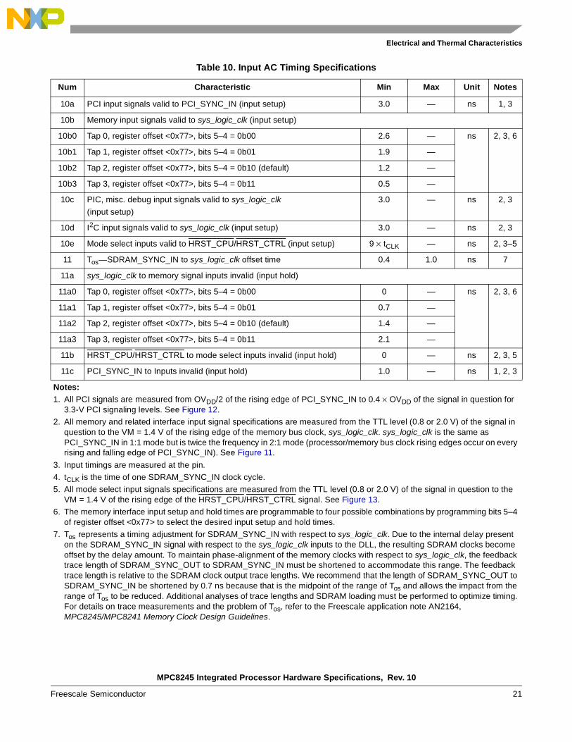
Table 10. Input AC Timing Specifications
Num Characteristic Min Max Unit Notes
10a PCI input signals valid to PCI_SYNC_IN (input setup) 3.0 — ns 1, 3
10b Memory input signals valid to sys_logic_clk (input setup)
10b0 Tap 0, register offset <0x77>, bits 5–4 = 0b00 2.6 — ns 2, 3, 6
10b1 Tap 1, register offset <0x77>, bits 5–4 = 0b01 1.9 —
10b2 Tap 2, register offset <0x77>, bits 5–4 = 0b10 (default) 1.2 —
10b3 Tap 3, register offset <0x77>, bits 5–4 = 0b11 0.5 —
10c PIC, misc. debug input signals valid to sys_logic_clk
(input setup)
3.0 — ns 2, 3
10d I2C input signals valid to sys_logic_clk (input setup) 3.0 — ns 2, 3
10e Mode select inputs valid to HRST_CPU/HRST_CTRL (input setup) 9 × tCLK — ns 2, 3–5
11 Tos—SDRAM_SYNC_IN to sys_logic_clk offset time 0.4 1.0 ns 7
11a sys_logic_clk to memory signal inputs invalid (input hold)
11a0 Tap 0, register offset <0x77>, bits 5–4 = 0b00 0 — ns 2, 3, 6
11a1 Tap 1, register offset <0x77>, bits 5–4 = 0b01 0.7 —
11a2 Tap 2, register offset <0x77>, bits 5–4 = 0b10 (default) 1.4 —
11a3 Tap 3, register offset <0x77>, bits 5–4 = 0b11 2.1 —
11b HRST_CPU/HRST_CTRL to mode select inputs invalid (input hold) 0 — ns 2, 3, 5
11c PCI_SYNC_IN to Inputs invalid (input hold) 1.0 — ns 1, 2, 3
Notes:1. All PCI signals are measured from OVDD/2 of the rising edge of PCI_SYNC_IN to 0.4 × OVDD of the signal in question for
3.3-V PCI signaling levels. See Figure 12.
2. All memory and related interface input signal specifications are measured from the TTL level (0.8 or 2.0 V) of the signal in question to the VM = 1.4 V of the rising edge of the memory bus clock, sys_logic_clk. sys_logic_clk is the same as PCI_SYNC_IN in 1:1 mode but is twice the frequency in 2:1 mode (processor/memory bus clock rising edges occur on every rising and falling edge of PCI_SYNC_IN). See Figure 11.
3. Input timings are measured at the pin.
4. tCLK is the time of one SDRAM_SYNC_IN clock cycle.
5. All mode select input signals specifications are measured from the TTL level (0.8 or 2.0 V) of the signal in question to the VM = 1.4 V of the rising edge of the HRST_CPU/HRST_CTRL signal. See Figure 13.
6. The memory interface input setup and hold times are programmable to four possible combinations by programming bits 5–4 of register offset <0x77> to select the desired input setup and hold times.
7. Tos represents a timing adjustment for SDRAM_SYNC_IN with respect to sys_logic_clk. Due to the internal delay present on the SDRAM_SYNC_IN signal with respect to the sys_logic_clk inputs to the DLL, the resulting SDRAM clocks become offset by the delay amount. To maintain phase-alignment of the memory clocks with respect to sys_logic_clk, the feedback trace length of SDRAM_SYNC_OUT to SDRAM_SYNC_IN must be shortened to accommodate this range. The feedback trace length is relative to the SDRAM clock output trace lengths. We recommend that the length of SDRAM_SYNC_OUT to SDRAM_SYNC_IN be shortened by 0.7 ns because that is the midpoint of the range of Tos and allows the impact from the range of Tos to be reduced. Additional analyses of trace lengths and SDRAM loading must be performed to optimize timing. For details on trace measurements and the problem of Tos, refer to the Freescale application note AN2164, MPC8245/MPC8241 Memory Clock Design Guidelines.
MPC8245 Integrated Processor Hardware Specifications, Rev. 10
22 Freescale Semiconductor
Electrical and Thermal Characteristics
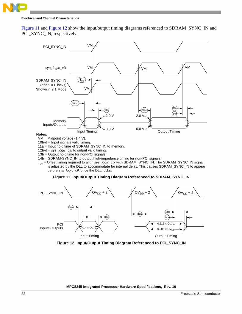
Figure 11 and Figure 12 show the input/output timing diagrams referenced to SDRAM_SYNC_IN and PCI_SYNC_IN, respectively.
Figure 11. Input/Output Timing Diagram Referenced to SDRAM_SYNC_IN
Figure 12. Input/Output Timing Diagram Referenced to PCI_SYNC_IN
11a
VM = Midpoint voltage (1.4 V).
Memory
10b-d
Inputs/Outputs
13b
14b
VMVM
SDRAM_SYNC_IN
Input Timing Output Timing
12b-d
2.0 V
0.8 V0.8 V
2.0 V
Tos
11a = Input hold time of SDRAM_SYNC_IN to memory.12b-d = sys_logic_clk to output valid timing.13b = Output hold time for non-PCI signals.14b = SDRAM-SYNC_IN to output high-impedance timing for non-PCI signals.Tos = Offset timing required to align sys_logic_clk with SDRAM_SYNC_IN. The SDRAM_SYNC_IN signal
sys_logic_clk VM
PCI_SYNC_IN VM
VM
is adjusted by the DLL to accommodate for internal delay. This causes SDRAM_SYNC_IN to appearbefore sys_logic_clk once the DLL locks.
(after DLL locks)Shown in 2:1 Mode
Notes:
10b-d = Input signals valid timing.
OVDD ÷ 2
10a
11c
PCI_SYNC_IN
PCI
12a13a
14a
OVDD ÷ 2OVDD ÷ 2
0.4 × OVDD
0.615 × OVDD
0.285 × OVDD
Input Timing Output Timing
Inputs/Outputs

MPC8245 Integrated Processor Hardware Specifications, Rev. 10
Freescale Semiconductor 23
Electrical and Thermal Characteristics
Figure 13 shows the input timing diagram for mode select signals.
Figure 13. Input Timing Diagram for Mode Select Signals
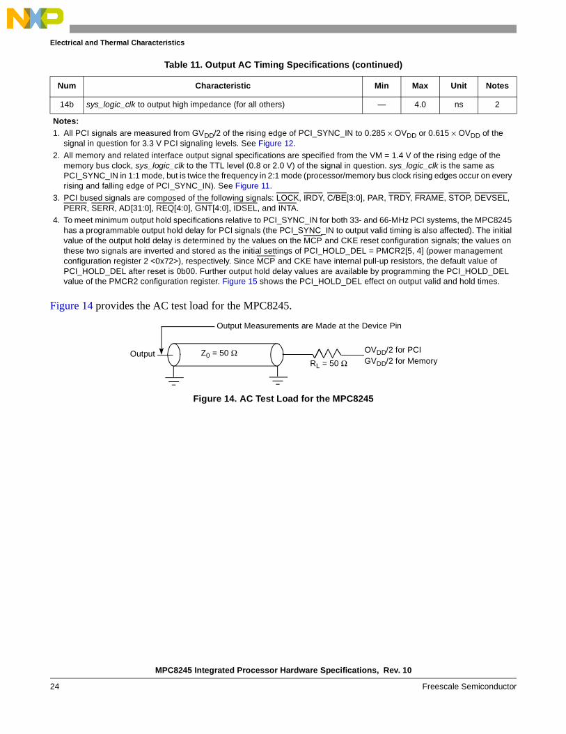
4.5.3 Output AC Timing SpecificationTable 11 provides the processor bus AC timing specifications for the MPC8245 at recommended operating conditions (see Table 2) with LVDD = 3.3 V ± 0.3 V. See Figure 11 for the input/output timing diagram referenced to sys_logic_clk. All output timings assume a purely resistive 50-Ω load (see Figure 14 for the AC test load for the MPC8245). Output timings are measured at the pin; time-of-flight delays must be added for trace lengths, vias, and connectors in the system. These specifications are for the default driver strengths indicated in Table 4.
Table 11. Output AC Timing Specifications
Num Characteristic Min Max Unit Notes
12a PCI_SYNC_IN to output valid, see Figure 15
12a0 Tap 0, PCI_HOLD_DEL=00, [MCP,CKE] = 11, 66 MHz PCI (default) — 6.0 ns 1, 3
12a1 Tap 1, PCI_HOLD_DEL=01, [MCP,CKE] = 10 — 6.5
12a2 Tap 2, PCI_HOLD_DEL=10, [MCP,CKE] = 01, 33 MHz PCI — 7.0
12a3 Tap 3, PCI_HOLD_DEL=11, [MCP,CKE] = 00 — 7.5
12b sys_logic_clk to output valid (memory control, address, and data signals) — 4.0 ns 2
12c sys_logic_clk to output valid (for all others) — 7.0 ns 2
12d sys_logic_clk to output valid (for I2C) — 5.0 ns 2
12e sys_logic_clk to output valid (ROM/Flash/PortX) — 6.0 ns 2
13a Output hold (PCI), see Figure 15
13a0 Tap 0, PCI_HOLD_DEL=00, [MCP,CKE] = 11, 66-MHz PCI (default) 2.0 — ns 1, 3, 4
13a1 Tap 1, PCI_HOLD_DEL=01, [MCP,CKE] = 10 2.5 —
13a2 Tap 2, PCI_HOLD_DEL=10, [MCP,CKE] = 01, 33-MHz PCI 3.0 —
13a3 Tap 3, PCI_HOLD_DEL=11, [MCP,CKE] = 00 3.5 —
13b Output hold (all others) 1.0 — ns 2
14a PCI_SYNC_IN to output high impedance (for PCI) — 14.0 ns 1, 3
VM
VM = Midpoint Voltage (1.4 V)
11b
Mode Pins
10e
HRST_CPU/HRST_CTRL
2.0 V
0.8 V
MPC8245 Integrated Processor Hardware Specifications, Rev. 10
24 Freescale Semiconductor
Electrical and Thermal Characteristics
Figure 14 provides the AC test load for the MPC8245.
Figure 14. AC Test Load for the MPC8245
14b sys_logic_clk to output high impedance (for all others) — 4.0 ns 2
Notes:1. All PCI signals are measured from GVDD/2 of the rising edge of PCI_SYNC_IN to 0.285 × OVDD or 0.615 × OVDD of the
signal in question for 3.3 V PCI signaling levels. See Figure 12.
2. All memory and related interface output signal specifications are specified from the VM = 1.4 V of the rising edge of the memory bus clock, sys_logic_clk to the TTL level (0.8 or 2.0 V) of the signal in question. sys_logic_clk is the same as PCI_SYNC_IN in 1:1 mode, but is twice the frequency in 2:1 mode (processor/memory bus clock rising edges occur on every rising and falling edge of PCI_SYNC_IN). See Figure 11.
3. PCI bused signals are composed of the following signals: LOCK, IRDY, C/BE[3:0], PAR, TRDY, FRAME, STOP, DEVSEL, PERR, SERR, AD[31:0], REQ[4:0], GNT[4:0], IDSEL, and INTA.
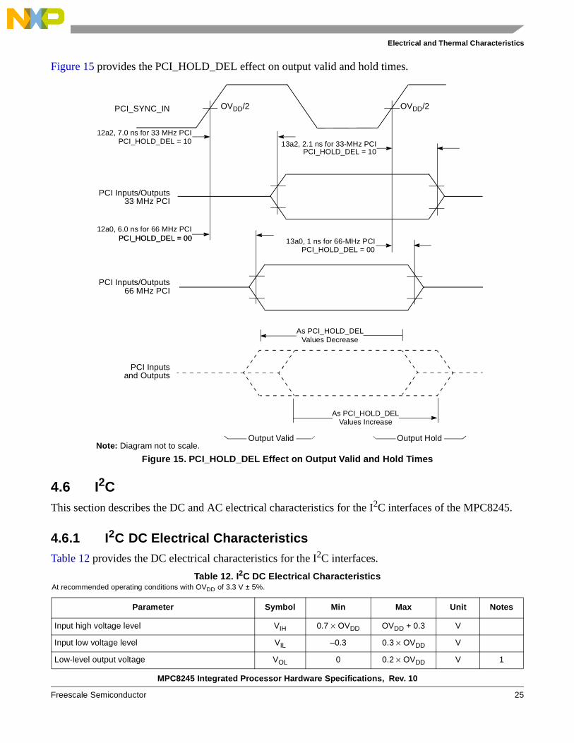
4. To meet minimum output hold specifications relative to PCI_SYNC_IN for both 33- and 66-MHz PCI systems, the MPC8245 has a programmable output hold delay for PCI signals (the PCI_SYNC_IN to output valid timing is also affected). The initial value of the output hold delay is determined by the values on the MCP and CKE reset configuration signals; the values on these two signals are inverted and stored as the initial settings of PCI_HOLD_DEL = PMCR2[5, 4] (power management configuration register 2 <0x72>), respectively. Since MCP and CKE have internal pull-up resistors, the default value of PCI_HOLD_DEL after reset is 0b00. Further output hold delay values are available by programming the PCI_HOLD_DEL value of the PMCR2 configuration register. Figure 15 shows the PCI_HOLD_DEL effect on output valid and hold times.
Table 11. Output AC Timing Specifications (continued)
Num Characteristic Min Max Unit Notes
Output Z0 = 50 Ω OVDD/2 for PCI
RL = 50 Ω
Output Measurements are Made at the Device Pin
GVDD/2 for Memory
MPC8245 Integrated Processor Hardware Specifications, Rev. 10
Freescale Semiconductor 25
Electrical and Thermal Characteristics
Figure 15 provides the PCI_HOLD_DEL effect on output valid and hold times.
Figure 15. PCI_HOLD_DEL Effect on Output Valid and Hold Times
4.6 I2C This section describes the DC and AC electrical characteristics for the I2C interfaces of the MPC8245.
4.6.1 I2C DC Electrical CharacteristicsTable 12 provides the DC electrical characteristics for the I2C interfaces.
Table 12. I2C DC Electrical CharacteristicsAt recommended operating conditions with OVDD of 3.3 V ± 5%.
Parameter Symbol Min Max Unit Notes
Input high voltage level VIH 0.7 × OVDD OVDD + 0.3 V
Input low voltage level VIL –0.3 0.3 × OVDD V
Low-level output voltage VOL 0 0.2 × OVDD V 1
PCI_SYNC_IN
PCI Inputs/Outputs33 MHz PCI
12a2, 7.0 ns for 33 MHz PCIPCI_HOLD_DEL = 10
12a0, 6.0 ns for 66 MHz PCIPCI_HOLD_DEL = 00
13a2, 2.1 ns for 33-MHz PCIPCI_HOLD_DEL = 10
13a0, 1 ns for 66-MHz PCIPCI_HOLD_DEL = 00
Output Valid Output HoldNote: Diagram not to scale.
As PCI_HOLD_DELValues Decrease
PCI Inputsand Outputs
PCI Inputs/Outputs66 MHz PCI
PCI_HOLD_DEL = 00
As PCI_HOLD_DELValues Increase
OVDD/2 OVDD/2
MPC8245 Integrated Processor Hardware Specifications, Rev. 10
26 Freescale Semiconductor
Electrical and Thermal Characteristics
4.6.2 I2C AC Electrical SpecificationsTable 13 provides the AC timing parameters for the I2C interfaces.
Pulse width of spikes which must be suppressed by the input filter
tI2KHKL 0 50 ns 2
Input current each I/O pin (input voltage is between 0.1 × OVDD and 0.9 × OVDD(max)
II –10 10 μA 3
Capacitance for each I/O pin CI — 10 pF
Notes:1. Output voltage (open drain or open collector) condition = 3 mA sink current.
2. Refer to the MPC8245 Integrated Processor Reference Manual for information on the digital filter used.
3. I/O pins obstruct the SDA and SCL lines if the OVDD is switched off.
Table 13. I2C AC Electrical SpecificationsAll values refer to VIH (min) and VIL (max) levels (see Table 12).
Parameter Symbol 1 Min Max Unit
SCL clock frequency fI2C 0 400 kHz
Low period of the SCL clock tI2CL 4 1.3 — μs
High period of the SCL clock tI2CH 4 0.6 — μs
Setup time for a repeated START condition tI2SVKH 4 0.6 — μs
Hold time (repeated) START condition (after this period, the first clock pulse is generated)
tI2SXKL 4 0.6 — μs
Data setup time tI2DVKH 4 100 — ns
Data input hold time:
CBUS compatible mastersI2C bus devices
tI2DXKL—0 2
——
μs
Data output delay time: tI2OVKL — 0.93
Set-up time for STOP condition tI2PVKH 0.6 — μs
Bus free time between a STOP and START condition tI2KHDX 1.3 — μs
Noise margin at the LOW level for each connected device (including hysteresis)
VNL 0.1 × OVDD — V
Table 12. I2C DC Electrical CharacteristicsAt recommended operating conditions with OVDD of 3.3 V ± 5%.
MPC8245 Integrated Processor Hardware Specifications, Rev. 10
Freescale Semiconductor 27
Electrical and Thermal Characteristics
Figure 16 provides the AC test load for the I2C.
Figure 16. I2C AC Test Load
Noise margin at the HIGH level for each connected device (including hysteresis)
VNH 0.2 × OVDD — V
Note: 1. The symbols used for timing specifications follow the pattern of t(first two letters of functional block)(signal)(state) (reference)(state) for
inputs and t(first two letters of functional block)(reference)(state)(signal)(state) for outputs. For example, tI2DVKH symbolizes I2C timing (I2) with respect to the time data input signals (D) reach the valid state (V) relative to the tI2C clock reference (K) going to the high (H) state or setup time. Also, tI2SXKL symbolizes I2C timing (I2) for the time that the data with respect to the start condition (S) went invalid (X) relative to the tI2C clock reference (K) going to the low (L) state or hold time. Also, tI2PVKH symbolizes I2C timing (I2) for the time that the data with respect to the stop condition (P) reaching the valid state (V) relative to the tI2C clock reference (K) going to the high (H) state or setup time. For rise and fall times, the latter convention is used with the appropriate letter: R (rise) or F (fall).
2. As a transmitter, the MPC8245 provides a delay time of at least 300 ns for the SDA signal (referred to as the Vihmin of the SCL signal) to bridge the undefined region of the falling edge of SCL to avoid unintended generation of Start or Stop condition. When the MPC8245acts as the I2C bus master while transmitting, it drives both SCL and SDA. As long as the load on SCL and SDA is balanced, the MPC8245 does not cause the unintended generation of a Start or Stop condition. Therefore, the 300 ns SDA output delay time is not a concern. If, under some rare condition, the 300 ns SDA output delay time is required for the MPC8245 as transmitter, the following setting is recommended for the FDR bit field of the I2CFDR register to ensure both the desired I2C SCL clock frequency and SDA output delay time are achieved. It is assumed that the desired I2C SCL clock frequency is 400 KHz and the digital filter sampling rate register (DFFSR bits in I2CFDR) is programmed with its default setting of 0x10 (decimal 16):
SDRAM Clock Frequency 100 MHz 133 MHz
FDR Bit Setting 0x00 0x2A
Actual FDR Divider Selected 384 896
Actual I2C SCL Frequency Generated 260.4 KHz 148.4 KHz
For details on I2C frequency calculation, refer to the application note AN2919 “Determining the I2C Frequency Divider Ratio for SCL”.
3. The maximum tI2DXKL has only to be met if the device does not stretch the LOW period (tI2CL) of the SCL signal.
4. Guaranteed by design.
Table 13. I2C AC Electrical Specifications (continued)All values refer to VIH (min) and VIL (max) levels (see Table 12).
Parameter Symbol 1 Min Max Unit
Output Z0 = 50 Ω OVDD/2RL = 50 Ω
MPC8245 Integrated Processor Hardware Specifications, Rev. 10
28 Freescale Semiconductor
Electrical and Thermal Characteristics
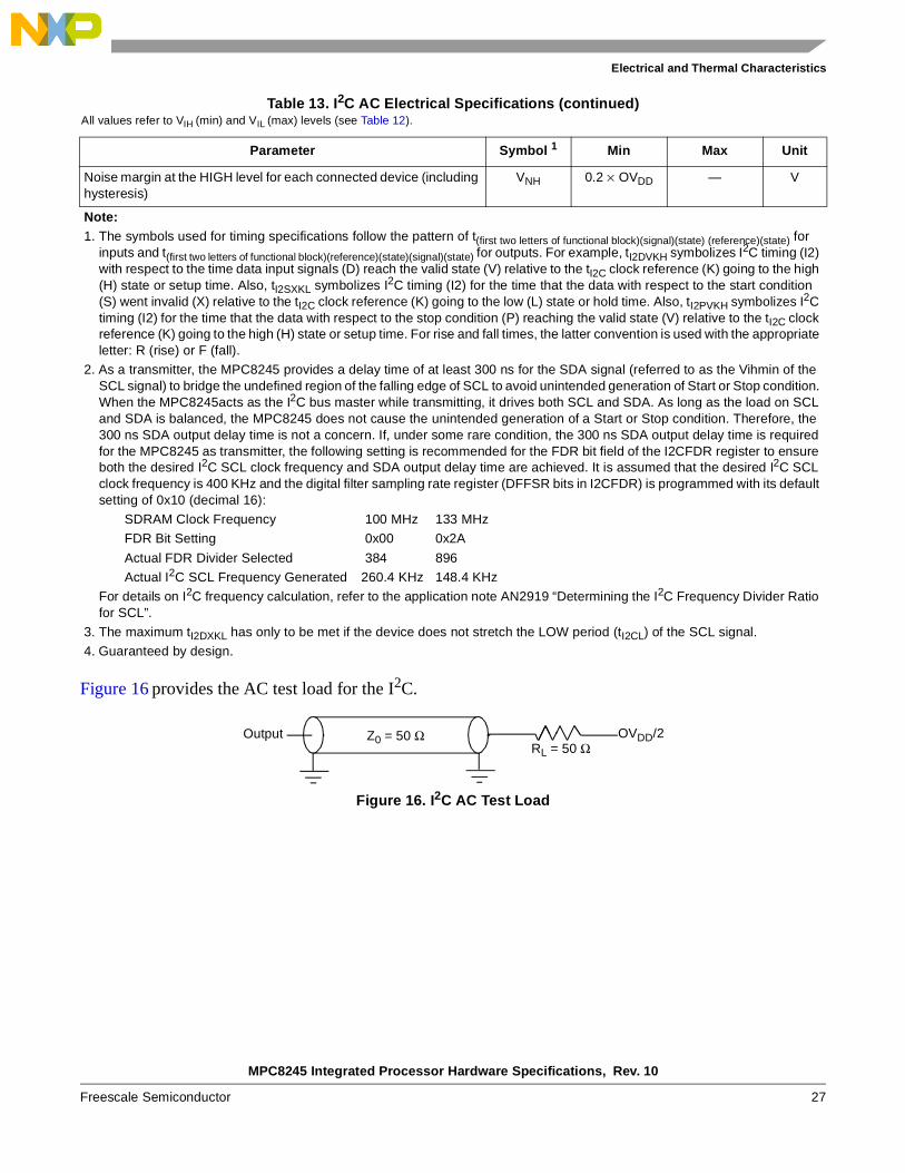
Figure 17 shows the AC timing diagram for the I2C bus.
Figure 17. I2C Bus AC Timing Diagram
4.7 PIC Serial Interrupt Mode AC Timing SpecificationsTable 14 provides the PIC serial interrupt mode AC timing specifications for the MPC8245 at recommended operating conditions (see Table 2) with GVDD = 3.3 V ± 5% and LVDD = 3.3 V ± 0.3 V.
Table 14. PIC Serial Interrupt Mode AC Timing Specifications
Num Characteristic Min Max Unit Notes
1 S_CLK frequency 1/14 SDRAM_SYNC_IN 1/2 SDRAM_SYNC_IN MHz 1
2 S_CLK duty cycle 40 60 % —
3 S_CLK output valid time — 6 ns —
4 Output hold time 0 — ns —
5 S_FRAME, S_RST output valid time — 1 sys_logic_clk period + 6 ns 2
6 S_INT input setup time to S_CLK 1 sys_logic_clk period + 2 — ns 2
7 S_INT inputs invalid (hold time) to S_CLK — 0 ns 2
Notes:1. See the MPC8245 Integrated Processor Reference Manual for a description of the PIC interrupt control register (ICR) and
S_CLK frequency programming.
2. S_RST, S_FRAME, and S_INT shown in Figure 18 and Figure 19, depict timing relationships to sys_logic_clk and S_CLK and do not describe functional relationships between S_RST, S_FRAME, and S_INT. The MPC8245 Integrated Processor Reference Manual describes the functional relationships between these signals.
3. The sys_logic_clk waveform is the clocking signal of the internal peripheral logic from the output of the peripheral logic PLL; sys_logic_clk is the same as SDRAM_SYNC_IN when the SDRAM_SYNC_OUT to SDRAM_SYNC_IN feedback loop is implemented and the DLL is locked. See the MPC8245 Integrated Processor Reference Manual for a complete clocking description.
SrS
SDA
SCL
tI2CF
tI2SXKL
tI2CL
tI2CHtI2DXKL,tI2OVKL
tI2DVKH
tI2SXKL
tI2SVKH
tI2KHKL
tI2PVKH
tI2CR
tI2CF
P S
MPC8245 Integrated Processor Hardware Specifications, Rev. 10
Freescale Semiconductor 29
Electrical and Thermal Characteristics
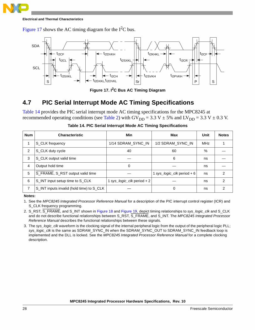
Figure 18. PIC Serial Interrupt Mode Output Timing Diagram
Figure 19. PIC Serial Interrupt Mode Input Timing Diagram
4.8 IEEE 1149.1 (JTAG) AC Timing SpecificationsTable 15 provides the JTAG AC timing specifications for the MPC8245 while in the JTAG operating mode at recommended operating conditions (see Table 2) with LVDD = 3.3 V ± 0.3 V. Timings are independent of the system clock (PCI_SYNC_IN).
Table 15. JTAG AC Timing Specification (Independent of PCI_SYNC_IN)
Num Characteristic Min Max Unit Notes
TCK frequency of operation 0 25 MHz
1 TCK cycle time 40 — ns
2 TCK clock pulse width measured at 1.5 V 20 — ns
3 TCK rise and fall times 0 3 ns
4 TRST setup time to TCK falling edge 10 — ns 1
5 TRST assert time 10 — ns
6 Input data setup time 5 — ns 2
7 Input data hold time 15 — ns 2
8 TCK to output data valid 0 30 ns 3
9 TCK to output high impedance 0 30 ns 3
10 TMS, TDI data setup time 5 — ns
S_CLK
S_RST
VM
VM
VM
S_FRAME
sys_logic_clk
VM
VM
VM
VM
43
5 4
6
S_CLK
S_INT
7
VM
MPC8245 Integrated Processor Hardware Specifications, Rev. 10
30 Freescale Semiconductor
Electrical and Thermal Characteristics
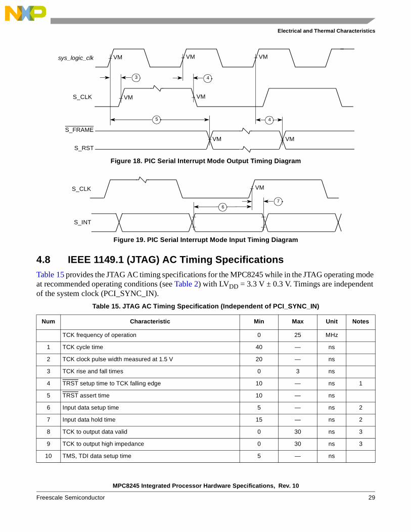
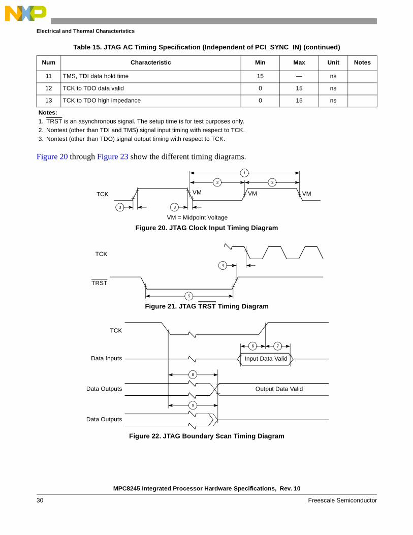
Figure 20 through Figure 23 show the different timing diagrams.
Figure 20. JTAG Clock Input Timing Diagram
Figure 21. JTAG TRST Timing Diagram
Figure 22. JTAG Boundary Scan Timing Diagram
11 TMS, TDI data hold time 15 — ns
12 TCK to TDO data valid 0 15 ns
13 TCK to TDO high impedance 0 15 ns
Notes:1. TRST is an asynchronous signal. The setup time is for test purposes only.
2. Nontest (other than TDI and TMS) signal input timing with respect to TCK.
3. Nontest (other than TDO) signal output timing with respect to TCK.
Table 15. JTAG AC Timing Specification (Independent of PCI_SYNC_IN) (continued)
Num Characteristic Min Max Unit Notes
TCK
22
1
VMVMVM
33
VM = Midpoint Voltage
4
5
TRST
TCK
6 7
Input Data Valid
8
9
Output Data Valid
TCK
Data Inputs
Data Outputs
Data Outputs
MPC8245 Integrated Processor Hardware Specifications, Rev. 10
Freescale Semiconductor 31
Package Description
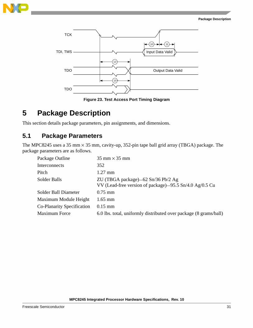
Figure 23. Test Access Port Timing Diagram
5 Package DescriptionThis section details package parameters, pin assignments, and dimensions.
5.1 Package ParametersThe MPC8245 uses a 35 mm × 35 mm, cavity-up, 352-pin tape ball grid array (TBGA) package. The package parameters are as follows.
Package Outline 35 mm × 35 mm
Interconnects 352
Pitch 1.27 mm
Solder Balls ZU (TBGA package)—62 Sn/36 Pb/2 AgVV (Lead-free version of package)—95.5 Sn/4.0 Ag/0.5 Cu
Solder Ball Diameter 0.75 mm
Maximum Module Height 1.65 mm
Co-Planarity Specification 0.15 mm
Maximum Force 6.0 lbs. total, uniformly distributed over package (8 grams/ball)
10 11
Input Data Valid
12
13
Output Data Valid
TCK
TDI, TMS
TDO
TDO
MPC8245 Integrated Processor Hardware Specifications, Rev. 10
32 Freescale Semiconductor
Package Description
5.2 Pin Assignments and Package DimensionsFigure 24 shows the top surface, side profile, and pinout of the MPC8245, 352 TBGA package.
Figure 24. MPC8245 Package Dimensions and Pinout Assignments
B
A
C
– E –
– F –
0.150
– T –
T
H
G
25 23 21 19 17 15 13 11 9 7 5 3 1
A
C
E
G
J
L
N
R
U
W
AA
AC
AE
352X ∅ D
MIN MAX
A 34.8 35.2
B 34.8 35.2
C 1.45 1.65
D .60 .90
G 1.27 BASIC
H .85 .95
K 31.75 BASIC
L .50 .70
Top View
Notes:
26 24 22 20 18 16 14 12 10 8 6 4 2
B
D
F
H
K
M
P
T
V
Y
AB
AD
AF
CORNER
K
L
Bottom View
1. Drawing not to scale.2. All measurements are in millimeters (mm).
K
Dot on top indicatescorner of A1 pin on bottom

MPC8245 Integrated Processor Hardware Specifications, Rev. 10
Freescale Semiconductor 33
Package Description
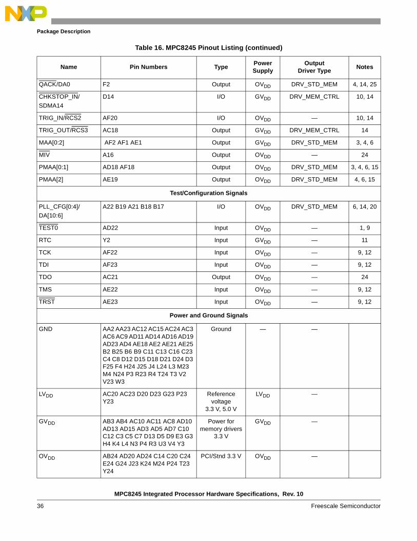
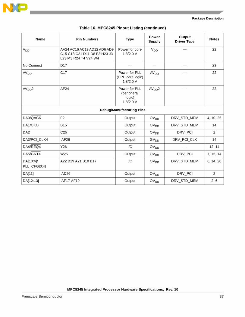
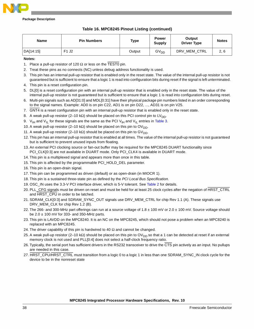
5.3 Pinout ListingsTable 16 provides the pinout listing for the MPC8245, 352 TBGA package.
Table 16. MPC8245 Pinout Listing
Name Pin Numbers TypePowerSupply
OutputDriver Type
Notes
PCI Interface Signals
C/BE[3:0] P25 K23 F23 A25 I/O OVDD DRV_PCI 6, 15
DEVSEL H26 I/O OVDD DRV_PCI 8, 15
FRAME J24 I/O OVDD DRV_PCI 8, 15
IRDY K25 I/O OVDD DRV_PCI 8, 15
LOCK J26 Input OVDD — 8
AD[31:0] V25 U25 U26 U24 U23 T25 T26 R25 R26 N26 N25 N23 M26 M25 L25 L26 F24 E26 E25 E23 D26 D25 C26 A26 B26 A24 B24 D19 B23 B22 D22 C22
I/O OVDD DRV_PCI 6, 15
PAR G25 I/O OVDD DRV_PCI 15
GNT[3:0] W25 W24 W23 V26 Output OVDD DRV_PCI 6, 15
GNT4/DA5 W26 Output OVDD DRV_PCI 7, 15, 14
REQ[3:0] Y25 AA26 AA25 AB26 Input OVDD — 6, 12
REQ4/DA4 Y26 I/O OVDD — 12, 14
PERR G26 I/O OVDD DRV_PCI 8, 15, 18
SERR F26 I/O OVDD DRV_PCI 8, 15, 16
STOP H25 I/O OVDD DRV_PCI 8, 15
TRDY K26 I/O OVDD DRV_PCI 8, 15
INTA AC26 Output OVDD DRV_PCI 10, 15, 16
IDSEL P26 Input OVDD —
Memory Interface Signals
MDL[0:31] AD17 AE17 AE15 AF15 AC14 AE13 AF13 AF12 AF11 AF10 AF9 AD8 AF8 AF7 AF6 AE5 B1 A1 A3 A4 A5 A6 A7 D7 A8 B8 A10 D10 A12 B11 B12 A14
I/O GVDD DRV_STD_MEM 5, 6
MDH[0:31] AC17 AF16 AE16 AE14 AF14 AC13 AE12 AE11 AE10 AE9 AE8 AC7 AE7 AE6 AF5 AC5 E4 A2 B3 D4 B4 B5 D6 C6 B7 C9 A9 B10 A11 A13 B13 A15
I/O GVDD DRV_STD_MEM 6
MPC8245 Integrated Processor Hardware Specifications, Rev. 10
34 Freescale Semiconductor
Package Description
DQM[0:7] AB1 AB2 K3 K2 AC1 AC2 K1 J1 Output GVDD DRV_MEM_CTRL 6
CS[0:7] Y4 AA3 AA4 AC4 M2 L2 M1 L1 Output GVDD DRV_MEM_CTRL 6
FOE H1 I/O GVDD DRV_MEM_CTRL 3, 4
RCS0 N4 Output GVDD DRV_MEM_CTRL 3, 4
RCS1 N2 Output GVDD DRV_MEM_CTRL
RCS2/TRIG_IN AF20 I/O OVDD 6 ohms 10, 14
RCS3/TRIG_OUT AC18 Output GVDD DRV_MEM_CTRL 14
SDMA[1:0] W1 W2 I/O GVDD DRV_MEM_CTRL 3, 4, 6
SDMA[11:2] N1 R1 R2 T1 T2 U4 U2 U1 V1 V3 Output GVDD DRV_MEM_CTRL 6
DRDY B20 Input OVDD — 9, 10
SDMA12/SRESET B16 I/O GVDD DRV_MEM_CTRL 10, 14
SDMA13/TBEN B14 I/O GVDD DRV_MEM_CTRL 10, 14
SDMA14/
CHKSTOP_IN
D14 I/O GVDD DRV_MEM_CTRL 10, 14
SDBA1 P1 Output GVDD DRV_MEM_CTRL
SDBA0 P2 Output GVDD DRV_MEM_CTRL
PAR[0:7] AF3 AE3 G4 E2 AE4 AF4 D2 C2 I/O GVDD DRV_STD_MEM 6
SDRAS AD1 Output GVDD DRV_MEM_CTRL 3
SDCAS AD2 Output GVDD DRV_MEM_CTRL 3
CKE H2 Output GVDD DRV_MEM_CTRL 3, 4
WE AA1 Output GVDD DRV_MEM_CTRL
AS Y1 Output GVDD DRV_MEM_CTRL 3, 4
PIC Control Signals
IRQ0/S_INT C19 Input OVDD —
IRQ1/S_CLK B21 I/O OVDD DRV_PCI
IRQ2/S_RST AC22 I/O OVDD DRV_PCI
IRQ3/S_FRAME AE24 I/O OVDD DRV_PCI
IRQ4/L_INT A23 I/O OVDD DRV_PCI
I2C Control Signals
SDA AE20 I/O OVDD DRV_STD_MEM 10, 16
SCL AF21 I/O OVDD DRV_STD_MEM 10, 16
Table 16. MPC8245 Pinout Listing (continued)
Name Pin Numbers TypePowerSupply
OutputDriver Type
Notes
MPC8245 Integrated Processor Hardware Specifications, Rev. 10
Freescale Semiconductor 35
Package Description
DUART Control Signals
SOUT1/PCI_CLK0 AC25 Output GVDD DRV_MEM_CTRL 13, 14
SIN1/PCI_CLK1 AB25 I/O GVDD DRV_MEM_CTRL 13, 14, 26
SOUT2/RTS1/
PCI_CLK2
AE26 Output GVDD DRV_MEM_CTRL 13, 14
SIN2/CTS1/
PCI_CLK3
AF25 I GVDD DRV_MEM_CTRL 13, 14, 26
Clock-Out Signals
PCI_CLK0/SOUT1 AC25 Output GVDD DRV_PCI_CLK 13, 14
PCI_CLK1/SIN1 AB25 Output GVDD DRV_PCI_CLK 13, 14, 26
PCI_CLK2/RTS1/
SOUT2
AE26 Output GVDD DRV_PCI_CLK 13, 14
PCI_CLK3/CTS1/
SIN2
AF25 Output GVDD DRV_PCI_CLK 13, 14, 26
PCI_CLK4/DA3 AF26 Output GVDD DRV_PCI_CLK 13, 14
PCI_SYNC_OUT AD25 Output GVDD DRV_PCI_CLK
PCI_SYNC_IN AB23 Input GVDD —
SDRAM_CLK [0:3] D1 G1 G2 E1 Output GVDD DRV_MEM_CTRL or
DRV_MEM_CLK
6, 21
SDRAM_SYNC_OUT C1 Output GVDD DRV_MEM_CTRLor
DRV_MEM_CLK
21
SDRAM_SYNC_IN H3 Input GVDD —
CKO/DA1 B15 Output OVDD DRV_STD_MEM 14
OSC_IN AD21 Input OVDD — 19
Miscellaneous Signals
HRST_CTRL A20 Input OVDD — 27
HRST_CPU A19 Input OVDD — 27
MCP A17 Output OVDD DRV_STD_MEM 3, 4, 17
NMI D16 Input OVDD —
SMI A18 Input OVDD — 10
SRESET/SDMA12 B16 I/O GVDD DRV_MEM_CTRL 10, 14
TBEN/SDMA13 B14 I/O GVDD DRV_MEM_CTRL 10, 14
Table 16. MPC8245 Pinout Listing (continued)
Name Pin Numbers TypePowerSupply
OutputDriver Type
Notes
MPC8245 Integrated Processor Hardware Specifications, Rev. 10
36 Freescale Semiconductor
Package Description
QACK/DA0 F2 Output OVDD DRV_STD_MEM 4, 14, 25
CHKSTOP_IN/
SDMA14
D14 I/O GVDD DRV_MEM_CTRL 10, 14
TRIG_IN/RCS2 AF20 I/O OVDD — 10, 14
TRIG_OUT/RCS3 AC18 Output GVDD DRV_MEM_CTRL 14
MAA[0:2] AF2 AF1 AE1 Output GVDD DRV_STD_MEM 3, 4, 6
MIV A16 Output OVDD — 24
PMAA[0:1] AD18 AF18 Output OVDD DRV_STD_MEM 3, 4, 6, 15
PMAA[2] AE19 Output OVDD DRV_STD_MEM 4, 6, 15
Test/Configuration Signals
PLL_CFG[0:4]/
DA[10:6]
A22 B19 A21 B18 B17 I/O OVDD DRV_STD_MEM 6, 14, 20
TEST0 AD22 Input OVDD — 1, 9
RTC Y2 Input GVDD — 11
TCK AF22 Input OVDD — 9, 12
TDI AF23 Input OVDD — 9, 12
TDO AC21 Output OVDD — 24
TMS AE22 Input OVDD — 9, 12
TRST AE23 Input OVDD — 9, 12
Power and Ground Signals
GND AA2 AA23 AC12 AC15 AC24 AC3 AC6 AC9 AD11 AD14 AD16 AD19 AD23 AD4 AE18 AE2 AE21 AE25 B2 B25 B6 B9 C11 C13 C16 C23 C4 C8 D12 D15 D18 D21 D24 D3 F25 F4 H24 J25 J4 L24 L3 M23 M4 N24 P3 R23 R4 T24 T3 V2 V23 W3
Ground — —
LVDD AC20 AC23 D20 D23 G23 P23 Y23
Reference voltage
3.3 V, 5.0 V
LVDD —
GVDD AB3 AB4 AC10 AC11 AC8 AD10 AD13 AD15 AD3 AD5 AD7 C10 C12 C3 C5 C7 D13 D5 D9 E3 G3 H4 K4 L4 N3 P4 R3 U3 V4 Y3
Power for memory drivers
3.3 V
GVDD —
OVDD AB24 AD20 AD24 C14 C20 C24 E24 G24 J23 K24 M24 P24 T23 Y24
PCI/Stnd 3.3 V OVDD —
Table 16. MPC8245 Pinout Listing (continued)
Name Pin Numbers TypePowerSupply
OutputDriver Type
Notes
MPC8245 Integrated Processor Hardware Specifications, Rev. 10
Freescale Semiconductor 37
Package Description
VDD AA24 AC16 AC19 AD12 AD6 AD9 C15 C18 C21 D11 D8 F3 H23 J3 L23 M3 R24 T4 V24 W4
Power for core 1.8/2.0 V
VDD — 22
No Connect D17 — — — 23
AVDD C17 Power for PLL (CPU core logic)
1.8/2.0 V
AVDD — 22
AVDD2 AF24 Power for PLL(peripheral
logic)1.8/2.0 V
AVDD2 — 22
Debug/Manufacturing Pins
DA0/QACK F2 Output OVDD DRV_STD_MEM 4, 10, 25
DA1/CKO B15 Output OVDD DRV_STD_MEM 14
DA2 C25 Output OVDD DRV_PCI 2
DA3/PCI_CLK4 AF26 Output GVDD DRV_PCI_CLK 14
DA4/REQ4 Y26 I/O OVDD — 12, 14
DA5/GNT4 W26 Output OVDD DRV_PCI 7, 15, 14
DA[10:6]/
PLL_CFG[0:4]
A22 B19 A21 B18 B17 I/O OVDD DRV_STD_MEM 6, 14, 20
DA[11] AD26 Output OVDD DRV_PCI 2
DA[12:13] AF17 AF19 Output OVDD DRV_STD_MEM 2, 6
Table 16. MPC8245 Pinout Listing (continued)
Name Pin Numbers TypePowerSupply
OutputDriver Type
Notes
MPC8245 Integrated Processor Hardware Specifications, Rev. 10
38 Freescale Semiconductor
Package Description
DA[14:15] F1 J2 Output GVDD DRV_MEM_CTRL 2, 6
Notes:1. Place a pull-up resistor of 120 Ω or less on the TEST0 pin.
2. Treat these pins as no connects (NC) unless debug address functionality is used.
3. This pin has an internal pull-up resistor that is enabled only in the reset state. The value of the internal pull-up resistor is not guaranteed but is sufficient to ensure that a logic 1 is read into configuration bits during reset if the signal is left unterminated.
4. This pin is a reset configuration pin.
5. DL[0] is a reset configuration pin with an internal pull-up resistor that is enabled only in the reset state. The value of the internal pull-up resistor is not guaranteed but is sufficient to ensure that a logic 1 is read into configuration bits during reset.
6. Multi-pin signals such as AD[31:0] and MDL[0:31] have their physical package pin numbers listed in an order corresponding to the signal names. Example: AD0 is on pin C22, AD1 is on pin D22, ..., AD31 is on pin V25.
7. GNT4 is a reset configuration pin with an internal pull-up resistor that is enabled only in the reset state.
8. A weak pull-up resistor (2–10 kΩ) should be placed on this PCI control pin to LVDD.
9. VIH and VIL for these signals are the same as the PCI VIH and VIL entries in Table 3.
10. A weak pull-up resistor (2–10 kΩ) should be placed on this pin to OVDD.
11. A weak pull-up resistor (2–10 kΩ) should be placed on this pin to GVDD.
12. This pin has an internal pull-up resistor that is enabled at all times. The value of the internal pull-up resistor is not guaranteed but is sufficient to prevent unused inputs from floating.
13. An external PCI clocking source or fan-out buffer may be required for the MPC8245 DUART functionality since PCI_CLK[0:3] are not available in DUART mode. Only PCI_CLK4 is available in DUART mode.
14. This pin is a multiplexed signal and appears more than once in this table.
15. This pin is affected by the programmable PCI_HOLD_DEL parameter.
16. This pin is an open-drain signal.
17. This pin can be programmed as driven (default) or as open-drain (in MIOCR 1).
18. This pin is a sustained three-state pin as defined by the PCI Local Bus Specification.
19. OSC_IN uses the 3.3-V PCI interface driver, which is 5-V tolerant. See Table 2 for details.
20. PLL_CFG signals must be driven on reset and must be held for at least 25 clock cycles after the negation of HRST_CTRL and HRST_CPU in order to be latched.
21. SDRAM_CLK[0:3] and SDRAM_SYNC_OUT signals use DRV_MEM_CTRL for chip Rev 1.1 (A). These signals use DRV_MEM_CLK for chip Rev 1.2 (B).
22. The 266- and 300-MHz part offerings can run at a source voltage of 1.8 ± 100 mV or 2.0 ± 100 mV. Source voltage should be 2.0 ± 100 mV for 333- and 350-MHz parts.
23. This pin is LAVDD on the MPC8240. It is an NC on the MPC8245, which should not pose a problem when an MPC8240 is replaced with an MPC8245.
24. The driver capability of this pin is hardwired to 40 Ω and cannot be changed.
25. A weak pull-up resistor (2–10 kΩ) should be placed on this pin to OVDD so that a 1 can be detected at reset if an external memory clock is not used and PLL[0:4] does not select a half-clock frequency ratio.
26. Typically, the serial port has sufficient drivers in the RS232 transceiver to drive the CTS pin actively as an input. No pullups are needed in this case.
27. HRST_CPU/HRST_CTRL must transition from a logic 0 to a logic 1 in less than one SDRAM_SYNC_IN clock cycle for the device to be in the nonreset state
Table 16. MPC8245 Pinout Listing (continued)
Name Pin Numbers TypePowerSupply
OutputDriver Type
Notes
MPC8245 Integrated Processor Hardware Specifications, Rev. 10
Freescale Semiconductor 39
PLL Configurations
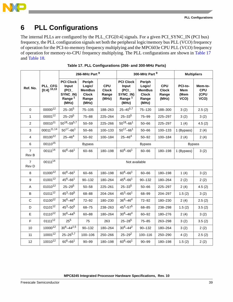
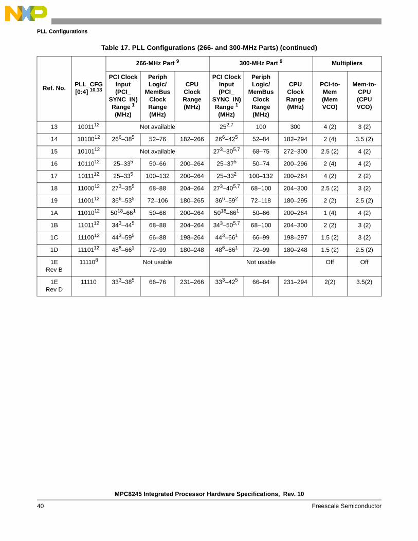
6 PLL ConfigurationsThe internal PLLs are configured by the PLL_CFG[0:4] signals. For a given PCI_SYNC_IN (PCI bus) frequency, the PLL configuration signals set both the peripheral logic/memory bus PLL (VCO) frequency of operation for the PCI-to-memory frequency multiplying and the MPC603e CPU PLL (VCO) frequency of operation for memory-to-CPU frequency multiplying. The PLL configurations are shown in Table 17 and Table 18.
Table 17. PLL Configurations (266- and 300-MHz Parts)
Ref. No.PLL_CFG[0:4] 10,13
266-MHz Part 9 300-MHz Part 9 Multipliers
PCI Clock Input (PCI_
SYNC_IN) Range 1
(MHz)
PeriphLogic/
MemBusClockRange(MHz)
CPUClockRange(MHz)
PCI Clock Input (PCI_
SYNC_IN) Range 1
(MHz)
PeriphLogic/
MemBusClockRange(MHz)
CPUClockRange(MHz)
PCI-to-Mem(MemVCO)
Mem-to-CPU(CPUVCO)
0 0000012 25–355 75–105 188–263 25–405,7 75–120 188–300 3 (2) 2.5 (2)
1 0000112 25–295 75–88 225–264 25–335 75–99 225–297 3 (2) 3 (2)
2 0001011 5018–595,7 50–59 225–266 5018–661 50–66 225–297 1 (4) 4.5 (2)
3 0001111,14 5017–661 50–66 100–133 5017–661 50–66 100–133 1 (Bypass) 2 (4)
4 0010012 25–464 50–92 100–184 25–464 50–92 100–184 2 (4) 2 (4)
6 0011015 Bypass Bypass Bypass
7Rev B
0011114 606–661 60–66 180–198 606–661 60–66 180–198 1 (Bypass) 3 (2)
7Rev D
0011114 Not available
8 0100012 606–661 60–66 180–198 606–661 60–66 180–198 1 (4) 3 (2)
9 0100112 456–661 90–132 180–264 456–661 90–132 180–264 2 (2) 2 (2)
A 0101012 25–295 50–58 225–261 25–335 50–66 225–297 2 (4) 4.5 (2)
B 0101112 453–595 68–88 204–264 453–661 68–99 204–297 1.5 (2) 3 (2)
C 0110012 366–464 72–92 180–230 366–464 72–92 180–230 2 (4) 2.5 (2)
D 0110112 453–505 68–75 238–263 453–575 68–85 238–298 1.5 (2) 3.5 (2)
E 0111012 306–445 60–88 180–264 306–464 60–92 180–276 2 (4) 3 (2)
F 0111112 255 75 263 25–285 75–85 263–298 3 (2) 3.5 (2)
10 1000012 306–442,5 90–132 180–264 306–442 90–132 180–264 3 (2) 2 (2)
11 1000112 25–265,7 100–106 250–266 25–292 100–116 250–290 4 (2) 2.5 (2)
12 1001012 606–661 90–99 180–198 606–661 90–99 180–198 1.5 (2) 2 (2)
MPC8245 Integrated Processor Hardware Specifications, Rev. 10
40 Freescale Semiconductor
PLL Configurations
13 1001112 Not available 252,7 100 300 4 (2) 3 (2)
14 1010012 266–385 52–76 182–266 266–425 52–84 182–294 2 (4) 3.5 (2)
15 1010112 Not available 273–305,7 68–75 272–300 2.5 (2) 4 (2)
16 1011012 25–335 50–66 200–264 25–375 50–74 200–296 2 (4) 4 (2)
17 1011112 25–335 100–132 200–264 25–332 100–132 200–264 4 (2) 2 (2)
18 1100012 273–355 68–88 204–264 273–405,7 68–100 204–300 2.5 (2) 3 (2)
19 1100112 366–535 72–106 180–265 366–592 72–118 180–295 2 (2) 2.5 (2)
1A 1101012 5018–661 50–66 200–264 5018–661 50–66 200–264 1 (4) 4 (2)
1B 1101112 343–445 68–88 204–264 343–505,7 68–100 204–300 2 (2) 3 (2)
1C 1110012 443–595 66–88 198–264 443–661 66–99 198–297 1.5 (2) 3 (2)
1D 1110112 486–661 72–99 180–248 486–661 72–99 180–248 1.5 (2) 2.5 (2)
1ERev B
111108 Not usable Not usable Off Off
1ERev D
11110 333–385 66–76 231–266 333–425 66–84 231–294 2(2) 3.5(2)
Table 17. PLL Configurations (266- and 300-MHz Parts) (continued)
Ref. No.PLL_CFG[0:4] 10,13
266-MHz Part 9 300-MHz Part 9 Multipliers
PCI Clock Input (PCI_
SYNC_IN) Range 1
(MHz)
PeriphLogic/
MemBusClockRange(MHz)
CPUClockRange(MHz)
PCI Clock Input (PCI_
SYNC_IN) Range 1
(MHz)
PeriphLogic/
MemBusClockRange(MHz)
CPUClockRange(MHz)
PCI-to-Mem(MemVCO)
Mem-to-CPU(CPUVCO)
MPC8245 Integrated Processor Hardware Specifications, Rev. 10
Freescale Semiconductor 41
PLL Configurations
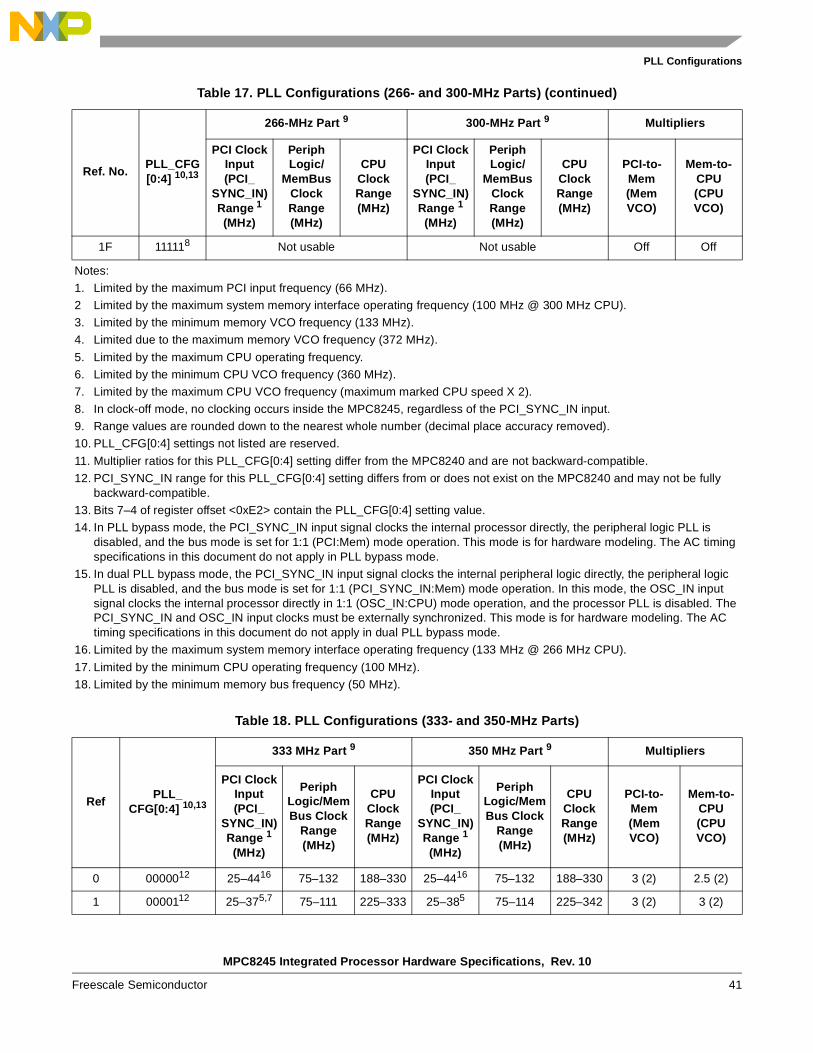
1F 111118 Not usable Not usable Off Off
Notes:
1. Limited by the maximum PCI input frequency (66 MHz).
2 Limited by the maximum system memory interface operating frequency (100 MHz @ 300 MHz CPU).
3. Limited by the minimum memory VCO frequency (133 MHz).
4. Limited due to the maximum memory VCO frequency (372 MHz).
5. Limited by the maximum CPU operating frequency.
6. Limited by the minimum CPU VCO frequency (360 MHz).
7. Limited by the maximum CPU VCO frequency (maximum marked CPU speed X 2).
8. In clock-off mode, no clocking occurs inside the MPC8245, regardless of the PCI_SYNC_IN input.
9. Range values are rounded down to the nearest whole number (decimal place accuracy removed).
10. PLL_CFG[0:4] settings not listed are reserved.
11. Multiplier ratios for this PLL_CFG[0:4] setting differ from the MPC8240 and are not backward-compatible.
12. PCI_SYNC_IN range for this PLL_CFG[0:4] setting differs from or does not exist on the MPC8240 and may not be fully backward-compatible.
13. Bits 7–4 of register offset <0xE2> contain the PLL_CFG[0:4] setting value.
14. In PLL bypass mode, the PCI_SYNC_IN input signal clocks the internal processor directly, the peripheral logic PLL is disabled, and the bus mode is set for 1:1 (PCI:Mem) mode operation. This mode is for hardware modeling. The AC timing specifications in this document do not apply in PLL bypass mode.
15. In dual PLL bypass mode, the PCI_SYNC_IN input signal clocks the internal peripheral logic directly, the peripheral logic PLL is disabled, and the bus mode is set for 1:1 (PCI_SYNC_IN:Mem) mode operation. In this mode, the OSC_IN input signal clocks the internal processor directly in 1:1 (OSC_IN:CPU) mode operation, and the processor PLL is disabled. The PCI_SYNC_IN and OSC_IN input clocks must be externally synchronized. This mode is for hardware modeling. The AC timing specifications in this document do not apply in dual PLL bypass mode.
16. Limited by the maximum system memory interface operating frequency (133 MHz @ 266 MHz CPU).
17. Limited by the minimum CPU operating frequency (100 MHz).
18. Limited by the minimum memory bus frequency (50 MHz).
Table 18. PLL Configurations (333- and 350-MHz Parts)
RefPLL_
CFG[0:4] 10,13
333 MHz Part 9 350 MHz Part 9 Multipliers
PCI Clock Input (PCI_
SYNC_IN) Range 1
(MHz)
Periph Logic/MemBus Clock
Range (MHz)
CPUClockRange (MHz)
PCI Clock Input (PCI_
SYNC_IN) Range 1
(MHz)
Periph Logic/MemBus Clock
Range (MHz)
CPUClockRange (MHz)
PCI-to-Mem(MemVCO)
Mem-to-CPU(CPUVCO)
0 0000012 25–4416 75–132 188–330 25–4416 75–132 188–330 3 (2) 2.5 (2)
1 0000112 25–375,7 75–111 225–333 25–385 75–114 225–342 3 (2) 3 (2)
Table 17. PLL Configurations (266- and 300-MHz Parts) (continued)
Ref. No.PLL_CFG[0:4] 10,13
266-MHz Part 9 300-MHz Part 9 Multipliers
PCI Clock Input (PCI_
SYNC_IN) Range 1
(MHz)
PeriphLogic/
MemBusClockRange(MHz)
CPUClockRange(MHz)
PCI Clock Input (PCI_
SYNC_IN) Range 1
(MHz)
PeriphLogic/
MemBusClockRange(MHz)
CPUClockRange(MHz)
PCI-to-Mem(MemVCO)
Mem-to-CPU(CPUVCO)

MPC8245 Integrated Processor Hardware Specifications, Rev. 10
42 Freescale Semiconductor
PLL Configurations
2 0001011 5018–661 50–66 225–297 5018–661 50–66 225–297 1 (4) 4.5 (2)
3 0001111,14 5017–661 50–66 100–133 5017–661 50–66 100–133 1 (Bypass) 2 (4)
4 0010012 25–464 50–92 100–184 25–464 50–92 100–184 2 (4) 2 (4)
6 0011015 Bypass Bypass Bypass
7Rev B
0011114 606–661 60–66 180–198 606–661 60–66 180–198 1 (Bypass) 3 (2)
7Rev D
0011114 Not available 25 100 350 4(2) 3.5(2)
8 0100012 606–661 60–66 180–198 606–661 60–66 180–198 1 (4) 3 (2)
9 0100112 456–661 90–132 180–264 456–661 90–132 180–264 2 (2) 2 (2)
A 0101012 25–375,7 50–74 225–333 25–385 50–76 225–342 2 (4) 4.5 (2)
B 0101112 453–661 68–99 204–297 453–661 68–99 204–297 1.5 (2) 3 (2)
C 0110012 366–464 72–92 180–230 366–464 72–92 180–230 2 (4) 2.5 (2)
D 0110112 453–635,7 68–95 238–333 453–661 68–99 238–347 1.5 (2) 3.5 (2)
E 0111012 306–464 60–92 180–276 306–464 60–92 180–276 2 (4) 3 (2)
F 0111112 25–315 75–93 263–326 25–335 75–99 263–347 3 (2) 3.5 (2)
10 1000012 306–442 90–132 180–264 306–442 90–132 180–264 3 (2) 2 (2)
11 1000112 25–332,16 100–132 250–330 25–332,16 100–132 250–330 4 (2) 2.5 (2)
12 1001012 606–661 90–99 180–198 606–661 90–99 180–198 1.5 (2) 2 (2)
13 1001112 25–275 100–108 300–324 25–295 100–116 300–348 4 (2) 3 (2)
14 1010012 266–474 52–94 182–329 266–474 52–94 182–329 2 (4) 3.5 (2)
15 1010112 273–335 68–83 272–332 273–345 68–85 272–340 2.5 (2) 4 (2)
16 1011012 25–415 50–82 200–328 25–435 50–86 200–344 2 (4) 4 (2)
17 1011112 25–332 100–132 200–264 25–332 100–132 200–264 4 (2) 2 (2)
18 1100012 273–445 68–110 204–330 273–465 68–115 204–345 2.5 (2) 3 (2)
19 1100112 366–661 72–132 180–330 366–661 72–132 180–330 2 (2) 2.5 (2)
1A 1101012 5018–661 50–66 200–264 5018–661 50–66 200–264 1 (4) 4 (2)
1B 1101112 343–555 68–110 204–330 343–585 68–116 204–348 2 (2) 3 (2)
1C 1110012 443–661 66–99 198–297 443–661 66–99 198–297 1.5 (2) 3 (2)
1D 1110112 486–661 72–99 180–248 486–661 72–99 180–248 1.5 (2) 2.5(2)
Table 18. PLL Configurations (333- and 350-MHz Parts) (continued)
RefPLL_
CFG[0:4] 10,13
333 MHz Part 9 350 MHz Part 9 Multipliers
PCI Clock Input (PCI_
SYNC_IN) Range 1
(MHz)
Periph Logic/MemBus Clock
Range (MHz)
CPUClockRange (MHz)
PCI Clock Input (PCI_
SYNC_IN) Range 1
(MHz)
Periph Logic/MemBus Clock
Range (MHz)
CPUClockRange (MHz)
PCI-to-Mem(MemVCO)
Mem-to-CPU(CPUVCO)
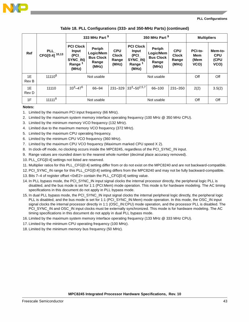
MPC8245 Integrated Processor Hardware Specifications, Rev. 10
Freescale Semiconductor 43
PLL Configurations
1ERev B
111108 Not usable Not usable Off Off
1ERev D
11110 333–475 66–94 231–329 333–502,5,7 66–100 231–350 2(2) 3.5(2)
1F 111118 Not usable Not usable Off Off
Notes:1. Limited by the maximum PCI input frequency (66 MHz).
2. Limited by the maximum system memory interface operating frequency (100 MHz @ 350 MHz CPU).
3. Limited by the minimum memory VCO frequency (132 MHz).
4. Limited due to the maximum memory VCO frequency (372 MHz).
5. Limited by the maximum CPU operating frequency.
6. Limited by the minimum CPU VCO frequency (360 MHz).
7. Limited by the maximum CPU VCO frequency (Maximum marked CPU speed X 2).
8. In clock-off mode, no clocking occurs inside the MPC8245, regardless of the PCI_SYNC_IN input.
9. Range values are rounded down to the nearest whole number (decimal place accuracy removed).
10. PLL_CFG[0:4] settings not listed are reserved.
11. Multiplier ratios for this PLL_CFG[0:4] setting differ from or do not exist on the MPC8240 and are not backward-compatible.
12. PCI_SYNC_IN range for this PLL_CFG[0:4] setting differs from the MPC8240 and may not be fully backward-compatible.
13. Bits 7–4 of register offset <0xE2> contain the PLL_CFG[0:4] setting value.
14. In PLL bypass mode, the PCI_SYNC_IN input signal clocks the internal processor directly, the peripheral logic PLL is disabled, and the bus mode is set for 1:1 (PCI:Mem) mode operation. This mode is for hardware modeling. The AC timing specifications in this document do not apply in PLL bypass mode.
15. In dual PLL bypass mode, the PCI_SYNC_IN input signal clocks the internal peripheral logic directly, the peripheral logic PLL is disabled, and the bus mode is set for 1:1 (PCI_SYNC_IN:Mem) mode operation. In this mode, the OSC_IN input signal clocks the internal processor directly in 1:1 (OSC_IN:CPU) mode operation, and the processor PLL is disabled. The PCI_SYNC_IN and OSC_IN input clocks must be externally synchronized. This mode is for hardware modeling. The AC timing specifications in this document do not apply in dual PLL bypass mode.
16. Limited by the maximum system memory interface operating frequency (133 MHz @ 333 MHz CPU).
17. Limited by the minimum CPU operating frequency (100 MHz).
18. Limited by the minimum memory bus frequency (50 MHz).
Table 18. PLL Configurations (333- and 350-MHz Parts) (continued)
RefPLL_
CFG[0:4] 10,13
333 MHz Part 9 350 MHz Part 9 Multipliers
PCI Clock Input (PCI_
SYNC_IN) Range 1
(MHz)
Periph Logic/MemBus Clock
Range (MHz)
CPUClockRange (MHz)
PCI Clock Input (PCI_
SYNC_IN) Range 1
(MHz)
Periph Logic/MemBus Clock
Range (MHz)
CPUClockRange (MHz)
PCI-to-Mem(MemVCO)
Mem-to-CPU(CPUVCO)
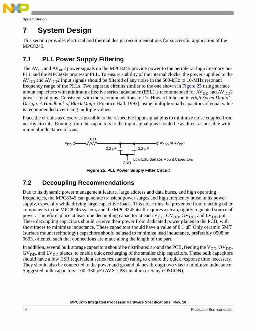
MPC8245 Integrated Processor Hardware Specifications, Rev. 10
44 Freescale Semiconductor
System Design
7 System DesignThis section provides electrical and thermal design recommendations for successful application of the MPC8245.
7.1 PLL Power Supply FilteringThe AVDD and AVDD2 power signals on the MPC8245 provide power to the peripheral logic/memory bus PLL and the MPC603e processor PLL. To ensure stability of the internal clocks, the power supplied to the AVDD and AVDD2 input signals should be filtered of any noise in the 500-kHz to 10-MHz resonant frequency range of the PLLs. Two separate circuits similar to the one shown in Figure 25 using surface mount capacitors with minimum effective series inductance (ESL) is recommended for AVDD and AVDD2 power signal pins. Consistent with the recommendations of Dr. Howard Johnson in High Speed Digital Design: A Handbook of Black Magic (Prentice Hall, 1993), using multiple small capacitors of equal value is recommended over using multiple values.
Place the circuits as closely as possible to the respective input signal pins to minimize noise coupled from nearby circuits. Routing from the capacitors to the input signal pins should be as direct as possible with minimal inductance of vias.
Figure 25. PLL Power Supply Filter Circuit
7.2 Decoupling RecommendationsDue to its dynamic power management feature, large address and data buses, and high operating frequencies, the MPC8245 can generate transient power surges and high frequency noise in its power supply, especially while driving large capacitive loads. This noise must be prevented from reaching other components in the MPC8245 system, and the MPC8245 itself requires a clean, tightly regulated source of power. Therefore, place at least one decoupling capacitor at each VDD, OVDD, GVDD, and LVDD pin. These decoupling capacitors should receive their power from dedicated power planes in the PCB, with short traces to minimize inductance. These capacitors should have a value of 0.1 µF. Only ceramic SMT (surface mount technology) capacitors should be used to minimize lead inductance, preferably 0508 or 0603, oriented such that connections are made along the length of the part.
In addition, several bulk storage capacitors should be distributed around the PCB, feeding the VDD, OVDD, GVDD, and LVDD planes, to enable quick recharging of the smaller chip capacitors. These bulk capacitors should have a low ESR (equivalent series resistance) rating to ensure the quick response time necessary. They should also be connected to the power and ground planes through two vias to minimize inductance. Suggested bulk capacitors: 100–330 µF (AVX TPS tantalum or Sanyo OSCON).
VDD AVDD or AVDD2
2.2 µF 2.2 µF
GNDLow ESL Surface Mount Capacitors
10 Ω
MPC8245 Integrated Processor Hardware Specifications, Rev. 10
Freescale Semiconductor 45
System Design
7.3 Connection RecommendationsTo ensure reliable operation, connect unused inputs to an appropriate signal level. Tie unused active-low inputs to OVDD. Connect unused active-high inputs tie to GND. All NC signals must remain unconnected.
Power and ground connections must be made to all external VDD, OVDD, GVDD, LVDD, and GND pins.
The PCI_SYNC_OUT signal is to be routed halfway out to the PCI devices and returned to the PCI_SYNC_IN input of the MPC8245.
The SDRAM_SYNC_OUT signal is to be routed halfway out to the SDRAM devices and then returned to the SDRAM_SYNC_IN input of the MPC8245. The trace length can be used to skew or adjust the timing window as needed. See the Tundra Tsi107™ Design Guide (AN1849) and Freescale application notes AN2164, MPC8245/MPC8241 Memory Clock Design Guidelines: Part 1 and AN2746, MPC8245/MPC8241 Memory Clock Design Guidelines: Part 2 for details. Note that there is an SDRAM_SYNC_IN to PCI_SYNC_IN time requirement (refer to Table 10 for the input AC timing specifications).
7.4 Pull-Up/Pull-Down Resistor RequirementsThe data bus input receivers are normally turned off when no read operation is in progress; therefore, they do not require pull-up resistors on the bus. The data bus signals are: MDH[0:31], MDL[0:31], and PAR[0:7].
If the 32-bit data bus mode is selected, the input receivers of the unused data and parity bits (MDL[0:31] and PAR[4:7]) are disabled, and their outputs drive logic zeros when they would otherwise normally be driven. For this mode, these pins do not require pull-up resistors and should be left unconnected to minimize possible output switching.
The TEST0 pin requires a pull-up resistor of 120 Ω or less connected to OVDD.
RTC should have weak pull-up resistors (2–10 kΩ) connected to GVDD.
The following signals should be pulled up to OVDD with weak pull-up resistors (2–10 kΩ): SDA, SCL, SMI, SRESET/SDMA12, TBEN/SDMA13, CHKSTOP_IN/SDMA14, TRIG_IN/RCS2, INTA, QACK/DA0 and DRDY. Note that QACK/DA0 should be left without a pull-up resistor only if an external clock is used because this signal enables internal clock flipping logic when it is low on reset, which is necessary when the PLL[0:4] signals select a half-clock frequency ratio and an external PLL is used to drive the SDRAM device.
It is recommended that the following PCI control signals be pulled up to LVDD (the clamping voltage) with weak pull-up resistors (2–10 kΩ): DEVSEL, FRAME, IRDY, LOCK, PERR, SERR, STOP, and TRDY. The resistor values may need to be adjusted stronger to reduce induced noise on specific board designs.
The following pins have internal pull-up resistors enabled at all times: REQ[3:0], REQ4/DA4, TCK, TDI, TMS, and TRST. See Table 16.
The following pins have internal pull-up resistors enabled only while device is in the reset state: GNT4/DA5, MDL0, FOE, RCS0, SDRAS, SDCAS, CKE, AS, MCP, MAA[0:2], and PMAA[0:2]. See Table 16.
MPC8245 Integrated Processor Hardware Specifications, Rev. 10
46 Freescale Semiconductor
System Design
The following pins are reset configuration pins: GNT4/DA5, MDL[0], FOE, RCS0, CKE, AS, MCP, QACK/DA0, MAA[0:2], PMAA[0:2], SDMA[1:0], MDH[16:31], and PLL_CFG[0:4]/DA[10:15]. These pins are sampled during reset to configure the device. The PLL_CFG[0:4] signals are sampled a few clocks after the negation of HRST_CPU and HRST_CTRL.
Reset configuration pins should be tied to GND via 1-kΩ pull-down resistors to ensure a logic 0 level is read into the configuration bits during reset if the default logic 1 level is not desired.
Any other unused active low input pins should be tied to a logic-one level through weak pull-up resistors (2–10 kΩ) to the appropriate power supply listed in Table 16. Unused active high input pins should be tied to GND through weak pull-down resistors (2–10 kΩ).
7.5 PCI Reference Voltage—LVDDThe MPC8245 PCI reference voltage (LVDD) pins should be connected to a 3.3 ± 0.3 V power supply if interfacing the MPC8245 into a 3.3-V PCI bus system. Similarly, the LVDD pins should be connected to a 5.0 V ± 5% power supply if interfacing the MPC8245 into a 5-V PCI bus system. For either reference voltage, the MPC8245 always performs 3.3-V signaling as described in the PCI Local Bus Specification (Rev. 2.2). The MPC8245 tolerates 5-V signals when interfaced into a 5-V PCI bus system.
7.6 MPC8245 Compatibility with MPC8240The MPC8245 AC timing specifications are backward-compatible with those of the MPC8240, except for the requirements of item 11 in Table 10. Timing adjustments are needed as specified for Tos (SDRAM_SYNC_IN to sys_logic_clk offset) time requirements.
The MPC8245 does not support the SDRAM flow-through memory interface.
The nominal core VDD power supply changes from 2.5 V on the MPC8240 to 1.8/2.0 V on the MPC8245. See Table 2.
For example, the MPC8245 PLL_CFG[0:4] setting 0x02 (0b00010) has a different PCI-to-Mem and Mem-to-CPU multiplier ratio than the same setting on the MPC8240, so it is not backward-compatible. See Table 17.
Most of the MPC8240 PLL_CFG[0:4] settings are subsets of the PCI_SYNC_IN input frequency range accepted by the MPC8245. However, the parts are not fully backward-compatible since the ranges of the two parts do not always match. Modes 0x8 and 0x18 of the MPC8245 are not compatible with settings 0x8 and 0x18 on the MPC8240. See Table 17 and Table 18.
Two reset configuration signals on the MPC8245 are not used as reset configuration signals on the MPC8240: SDMA0 and SDMA1.
The SDMA0 reset configuration pin selects between the MPC8245 DUART and the MPC8240 backward-compatible mode PCI_CLK[0:4] functionality on these multiplexed signals. The default state (logic 1) of SDMA0 selects the MPC8240 backward-compatible mode of PCI_CLK[0:4] functionality while a logic 0 state on the SDMA0 signal selects DUART functionality. In DUART mode, four of the five PCI clocks, PCI_CLK[0:3], are not available.
The SDMA1 reset configuration pin selects between MPC8245 extended ROM functionality and MPC8240 backward-compatible functionality on the multiplexed signals: TBEN, CHKSTOP_IN,
MPC8245 Integrated Processor Hardware Specifications, Rev. 10
Freescale Semiconductor 47
System Design
SRESET, TRIG_IN, and TRIG_OUT. The default state (logic 1) of SDMA1 selects the MPC8240 backward-compatible mode functionality, while a logic 0 state on the SDMA1 signal selects extended ROM functionality. In extended ROM mode, the TBEN, CHKSTOP_IN, SRESET, TRIG_IN, and TRIG_OUT functionalities are not available.
The driver names and pin capability of the MPC8245 and the MPC8240 differ slightly. Refer to the drive capability table (for the ODCR register at 0x73) in the MPC8240 Integrated Processor Hardware Specifications and Table 4.
The programmable PCI output valid and output hold feature controlled by bits in the power management configuration register 2 (PMCR2) <0x72> differs slightly in the MPC8245. For the MPC8240, three bits, PMCR2[6:4] = PCI_HOLD_DEL, are used to select 1 of 8 possible PCI output timing configurations. PMCR2[6:5] are software-controllable but are initially set by the reset configuration state of the MCP and CKE signals, respectively. Software can change PMCR2[4]. The default configuration for PMCR2[6:4] = 0b110 since the MCP and CKE signals have internal pull-up resistors, but this default configuration does not select 33- or 66-MHz PCI operation output timing parameters for the MPC8240. Software makes this selection. For the MPC8245, only two bits in the power management configuration register 2 (PMCR2), PMCR2[5:4] = PCI_HOLD_DEL, control the variable PCI output timing. PMCR2[5:4] are software controllable but are initially set by the inverted reset configuration state of the MCP and CKE signals, respectively. The default configuration for PMCR2[5:4] = 0b00 since the MCP and CKE signals have internal pull-up resistors and the values from these signals are inverted; this default configuration selects 66-MHz PCI operation output timing parameters. There are four programmable PCI output timing configurations on the MPC8245. See Table 11.
Voltage sequencing requirements for the MPC8245 are similar to those for the MPC8240, with two exceptions in the MPC8245. In the MPC8245, the non-PCI input voltages (Vin) must not be greater than GVDD or OVDD by more than 0.6 V at all times, including during power-on reset (see Caution 5 in Table 2). Second, LVDD must not exceed OVDD by more than 3.0 V at any time, including during power-on reset (see Caution 10 in Table 2); the allowable separation between LVDD and OVDD is 3.6 V for the MPC8240.
There is no LAVDD input voltage supply signal on the MPC8245 since the SDRAM clock delay-locked loop (DLL) has power supplied internally. Signal D17 should be treated as a NC for the MPC8245. Application note AN2128 highlights the differences between the MPC8240 and the MPC8245.
7.7 JTAG Configuration SignalsBoundary scan testing is enabled through the JTAG interface signals. The TRST signal is optional in the IEEE 1149.1 specification but is provided on all processors that implement the Power Architecture technology. While the TAP controller can be forced to the reset state using only the TCK and TMS signals, more reliable power-on reset performance can be obtained if the TRST signal is asserted during power-on reset. Because the JTAG interface is also used for accessing the common on-chip processor (COP) function, simply tying TRST to HRESET is not practical.
The COP function of these processors allows a remote computer system (typically, a PC with dedicated hardware and debugging software) to access and control the internal operations of the processor. The COP interface connects primarily through the JTAG, with additional status monitoring signals. The COP port must independently assert HRESET or TRST to control the processor. If the target system has independent
MPC8245 Integrated Processor Hardware Specifications, Rev. 10
48 Freescale Semiconductor
System Design
reset sources, such as voltage monitors, watchdog timers, power supply failures, or push-button switches, the COP reset signals must be merged into these signals with logic.
The arrangement shown in Figure 26 allows the COP port to independently assert HRESET or TRST, while ensuring that the target can drive HRESET as well. If the JTAG interface and COP header will not be used, TRST should be tied to HRESET through a 0-Ω isolation resistor so that it is asserted when the system reset signal (HRESET) is asserted, ensuring that the JTAG scan chain is initialized during power-on. Although Freescale recommends that the COP header be designed into the system as shown in Figure 26, if this is not possible, the isolation resistor will allow future access to TRST in the case where a JTAG interface may need to be wired onto the system in debug situations.
The COP interface has a standard header for connection to the target system based on the 0.025" square-post, 0.100" centered header assembly (often called a Berg header). Typically, pin 14 is removed as a connector key.
There is no standardized way to number the COP header shown in Figure 26. Consequently, different emulator vendors number the pins differently. Some pins are numbered top-to-bottom and left-to-right while others use left-to-right then top-to-bottom and still others number the pins counter clockwise from pin 1 (as with an IC). Regardless of the numbering, the signal placement recommended in Figure 26 is common to all known emulators.
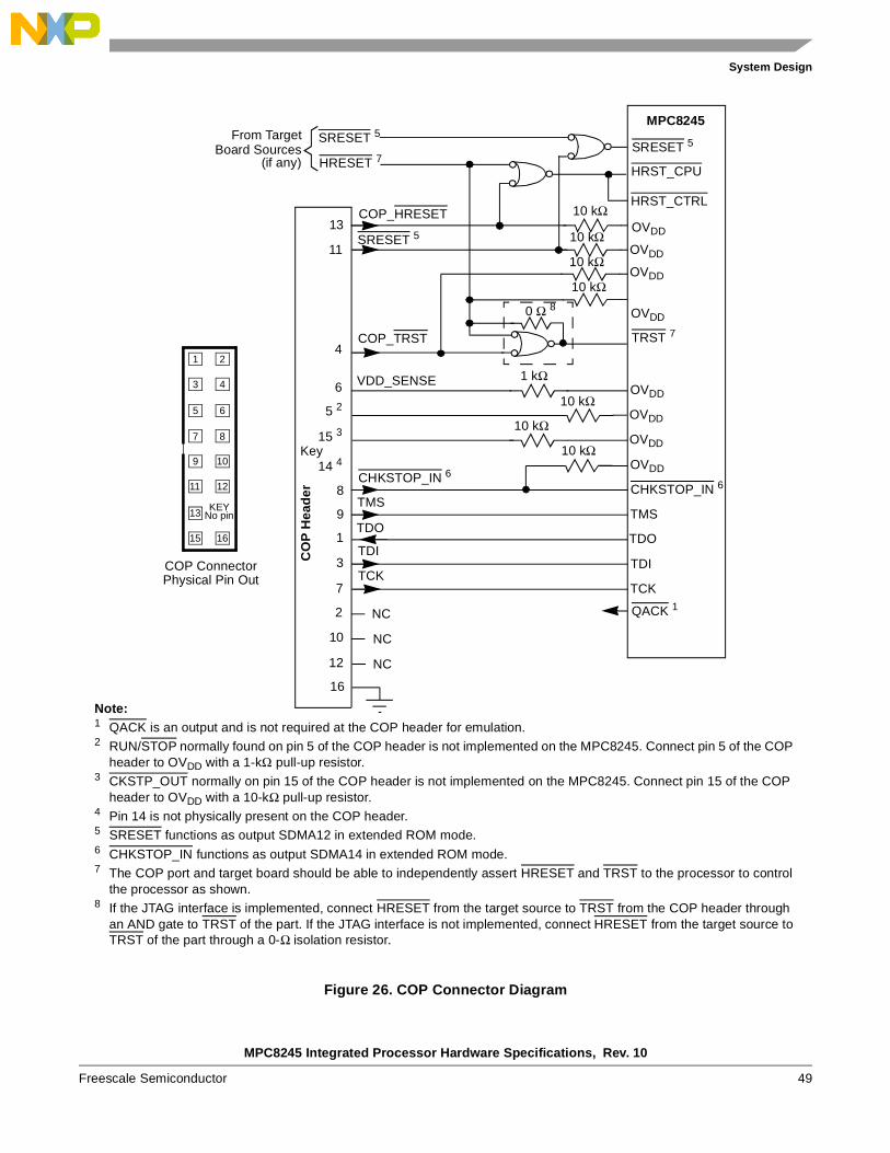
MPC8245 Integrated Processor Hardware Specifications, Rev. 10
Freescale Semiconductor 49
System Design
Figure 26. COP Connector Diagram
HRESET 7HRST_CPU
HRST_CTRL
From TargetBoard Sources
COP_HRESET13
SRESET 5
SRESET 5SRESET 5
NC
NC
NC
11
VDD_SENSE6
5 2
15 3
1 kΩ
10 kΩ
10 kΩ
10 kΩ
OVDD
OVDD
OVDD
OVDDCHKSTOP_IN 6
CHKSTOP_IN 68TMS
TDO
TDI
TCK
TMS
TDO
TDI
TCK
9
1
3
4COP_TRST
7
16
2
10
12
(if any)
CO
P H
ead
er
14 4Key
QACK 1
OVDD
OVDD
10 kΩ
OVDD
TRST 7
10 kΩOVDD
10 kΩ
10 kΩ
MPC8245
3
13
9
5
1
6
10
2
15
11
7
16
12
8
4
KEYNo pin
COP ConnectorPhysical Pin Out
0 Ω 8
Note: 1 QACK is an output and is not required at the COP header for emulation.2 RUN/STOP normally found on pin 5 of the COP header is not implemented on the MPC8245. Connect pin 5 of the COP
header to OVDD with a 1-kΩ pull-up resistor.3 CKSTP_OUT normally on pin 15 of the COP header is not implemented on the MPC8245. Connect pin 15 of the COP
header to OVDD with a 10-kΩ pull-up resistor.4 Pin 14 is not physically present on the COP header.5 SRESET functions as output SDMA12 in extended ROM mode.6 CHKSTOP_IN functions as output SDMA14 in extended ROM mode.7 The COP port and target board should be able to independently assert HRESET and TRST to the processor to control
the processor as shown.8 If the JTAG interface is implemented, connect HRESET from the target source to TRST from the COP header through
an AND gate to TRST of the part. If the JTAG interface is not implemented, connect HRESET from the target source to TRST of the part through a 0-Ω isolation resistor.
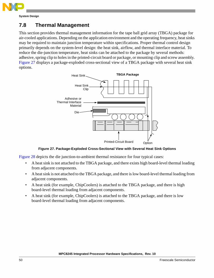
MPC8245 Integrated Processor Hardware Specifications, Rev. 10
50 Freescale Semiconductor
System Design
7.8 Thermal ManagementThis section provides thermal management information for the tape ball grid array (TBGA) package for air-cooled applications. Depending on the application environment and the operating frequency, heat sinks may be required to maintain junction temperature within specifications. Proper thermal control design primarily depends on the system-level design: the heat sink, airflow, and thermal interface material. To reduce the die-junction temperature, heat sinks can be attached to the package by several methods: adhesive, spring clip to holes in the printed-circuit board or package, or mounting clip and screw assembly. Figure 27 displays a package-exploded cross-sectional view of a TBGA package with several heat sink options.
Figure 27. Package-Exploded Cross-Sectional View with Several Heat Sink Options
Figure 28 depicts the die junction-to-ambient thermal resistance for four typical cases:
• A heat sink is not attached to the TBGA package, and there exists high board-level thermal loading from adjacent components.
• A heat sink is not attached to the TBGA package, and there is low board-level thermal loading from adjacent components.
• A heat sink (for example, ChipCoolers) is attached to the TBGA package, and there is high board-level thermal loading from adjacent components.
• A heat sink (for example, ChipCoolers) is attached to the TBGA package, and there is low board-level thermal loading from adjacent components.
Thermal Interface
Heat Sink TBGA Package
Heat SinkClip
Printed-Circuit Board Option
Material
Die
Adhesive or
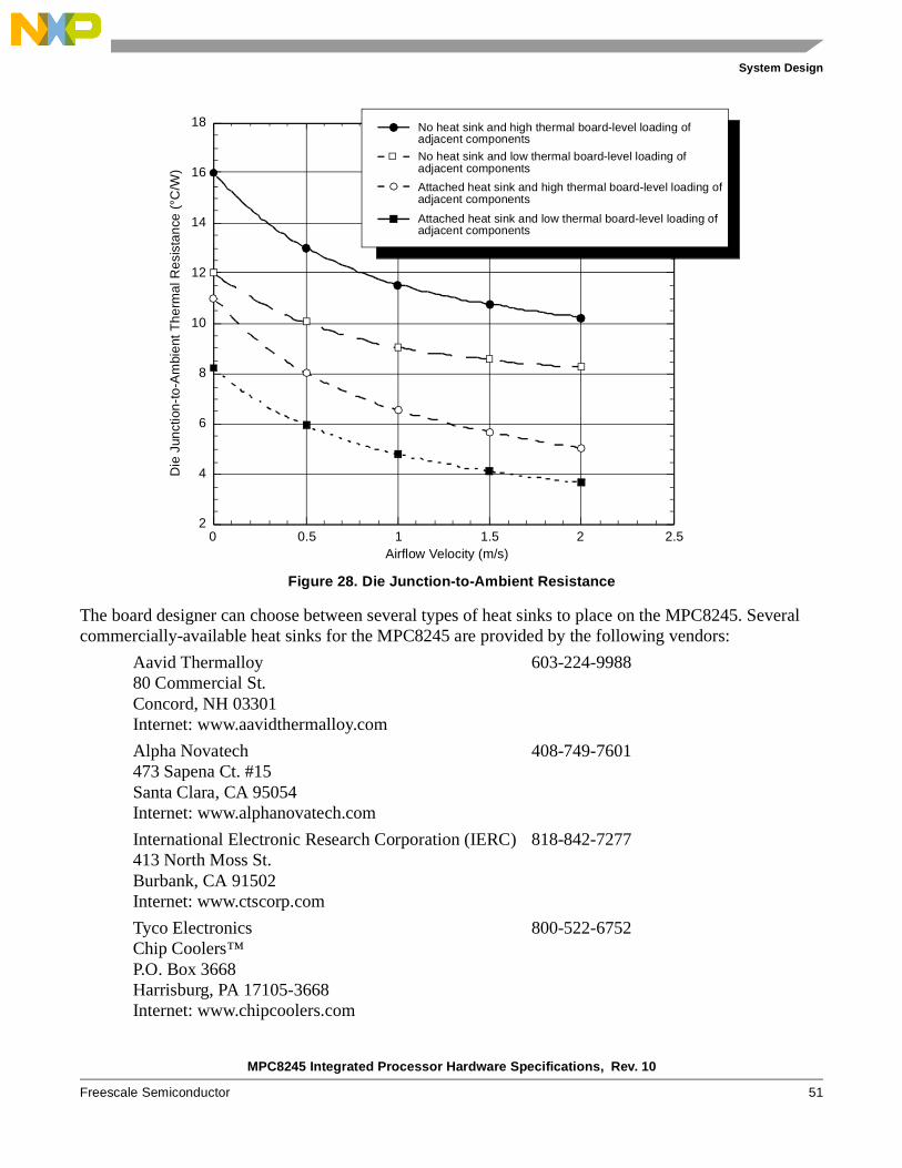
MPC8245 Integrated Processor Hardware Specifications, Rev. 10
Freescale Semiconductor 51
System Design
Figure 28. Die Junction-to-Ambient Resistance
The board designer can choose between several types of heat sinks to place on the MPC8245. Several commercially-available heat sinks for the MPC8245 are provided by the following vendors:
Aavid Thermalloy 603-224-998880 Commercial St.Concord, NH 03301Internet: www.aavidthermalloy.com
Alpha Novatech 408-749-7601473 Sapena Ct. #15Santa Clara, CA 95054Internet: www.alphanovatech.com
International Electronic Research Corporation (IERC) 818-842-7277413 North Moss St.Burbank, CA 91502Internet: www.ctscorp.com
Tyco Electronics 800-522-6752Chip Coolers™P.O. Box 3668Harrisburg, PA 17105-3668Internet: www.chipcoolers.com
2
4
6
8
10
12
14
16
18
0 0.5 1 1.5 2 2.5
Die
Jun
ctio
n-to
-Am
bien
t The
rmal
Res
ista
nce
(°C
/W)
Airflow Velocity (m/s)
No heat sink and high thermal board-level loading ofadjacent components
No heat sink and low thermal board-level loading ofadjacent components
Attached heat sink and high thermal board-level loading ofadjacent components
Attached heat sink and low thermal board-level loading ofadjacent components
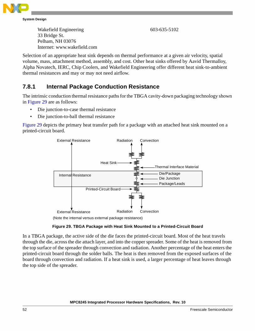
MPC8245 Integrated Processor Hardware Specifications, Rev. 10
52 Freescale Semiconductor
System Design
Wakefield Engineering 603-635-510233 Bridge St.Pelham, NH 03076Internet: www.wakefield.com
Selection of an appropriate heat sink depends on thermal performance at a given air velocity, spatial volume, mass, attachment method, assembly, and cost. Other heat sinks offered by Aavid Thermalloy, Alpha Novatech, IERC, Chip Coolers, and Wakefield Engineering offer different heat sink-to-ambient thermal resistances and may or may not need airflow.
7.8.1 Internal Package Conduction Resistance
The intrinsic conduction thermal resistance paths for the TBGA cavity-down packaging technology shown in Figure 29 are as follows:
• Die junction-to-case thermal resistance
• Die junction-to-ball thermal resistance
Figure 29 depicts the primary heat transfer path for a package with an attached heat sink mounted on a printed-circuit board.
Figure 29. TBGA Package with Heat Sink Mounted to a Printed-Circuit Board
In a TBGA package, the active side of the die faces the printed-circuit board. Most of the heat travels through the die, across the die attach layer, and into the copper spreader. Some of the heat is removed from the top surface of the spreader through convection and radiation. Another percentage of the heat enters the printed-circuit board through the solder balls. The heat is then removed from the exposed surfaces of the board through convection and radiation. If a heat sink is used, a larger percentage of heat leaves through the top side of the spreader.
External Resistance
External Resistance
Internal Resistance
Radiation Convection
Radiation Convection
Heat Sink
Printed-Circuit Board
Thermal Interface Material
Package/LeadsDie JunctionDie/Package
(Note the internal versus external package resistance)
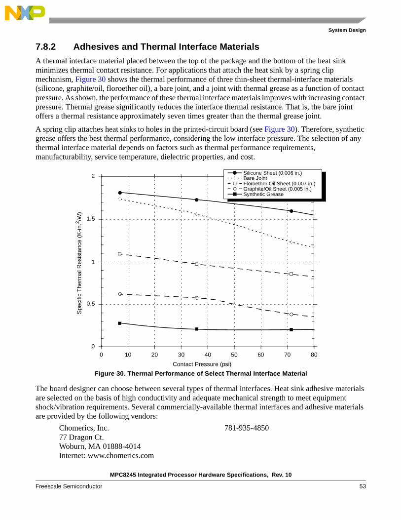
MPC8245 Integrated Processor Hardware Specifications, Rev. 10
Freescale Semiconductor 53
System Design
7.8.2 Adhesives and Thermal Interface MaterialsA thermal interface material placed between the top of the package and the bottom of the heat sink minimizes thermal contact resistance. For applications that attach the heat sink by a spring clip mechanism, Figure 30 shows the thermal performance of three thin-sheet thermal-interface materials (silicone, graphite/oil, floroether oil), a bare joint, and a joint with thermal grease as a function of contact pressure. As shown, the performance of these thermal interface materials improves with increasing contact pressure. Thermal grease significantly reduces the interface thermal resistance. That is, the bare joint offers a thermal resistance approximately seven times greater than the thermal grease joint.
A spring clip attaches heat sinks to holes in the printed-circuit board (see Figure 30). Therefore, synthetic grease offers the best thermal performance, considering the low interface pressure. The selection of any thermal interface material depends on factors such as thermal performance requirements, manufacturability, service temperature, dielectric properties, and cost.
Figure 30. Thermal Performance of Select Thermal Interface Material
The board designer can choose between several types of thermal interfaces. Heat sink adhesive materials are selected on the basis of high conductivity and adequate mechanical strength to meet equipment shock/vibration requirements. Several commercially-available thermal interfaces and adhesive materials are provided by the following vendors:
Chomerics, Inc. 781-935-485077 Dragon Ct.Woburn, MA 01888-4014Internet: www.chomerics.com
0
0.5
1
1.5
2
0 10 20 30 40 50 60 70 80
Silicone Sheet (0.006 in.)Bare JointFloroether Oil Sheet (0.007 in.)Graphite/Oil Sheet (0.005 in.)Synthetic Grease
Contact Pressure (psi)
Spe
cific
The
rmal
Res
ista
nce
(K-in
.2 /W)
MPC8245 Integrated Processor Hardware Specifications, Rev. 10
54 Freescale Semiconductor
System Design
Dow-Corning Corporation 800-248-2481Dow-Corning Electronic Materials2200 W. Salzburg Rd.Midland, MI 48686-0997Internet: www.dow.com
Shin-Etsu MicroSi, Inc. 888-642-767410028 S. 51st St.Phoenix, AZ 85044Internet: www.microsi.com
The Bergquist Company 800-347-457218930 West 78th St.Chanhassen, MN 55317Internet: www.bergquistcompany.com
Thermagon Inc. 888-246-90504707 Detroit Ave.Cleveland, OH 44102Internet: www.thermagon.com
7.8.3 Heat Sink UsageAn estimation of the chip junction temperature, TJ, can be obtained from the equation:
TJ = TA + (RθJA × PD)
where
TA = ambient temperature for the package (°C)RθJA = junction-to-ambient thermal resistance (°C/W)PD = power dissipation in the package (W)
The junction-to-ambient thermal resistance is an industry-standard value that provides a quick and easy estimation of thermal performance. Unfortunately, two values are in common usage: the value determined on a single-layer board and the value obtained on a board with two planes. Which value is closer to the application depends on the power dissipated by other components on the board. The value obtained on a single-layer board is appropriate for the tightly packed printed-circuit board. The value obtained on the board with the internal planes is usually appropriate if the board has low power dissipation and the components are well separated.
When a heat sink is used, the thermal resistance is expressed as the sum of a junction-to-case thermal resistance and a case-to-ambient thermal resistance:
RθJA = RθJC + RθCA
where
RθJA = junction-to-ambient thermal resistance (°C/W)RθJC = junction-to-case thermal resistance (°C/W)RθCA = case-to-ambient thermal resistance (°C/W)

MPC8245 Integrated Processor Hardware Specifications, Rev. 10
Freescale Semiconductor 55
System Design
RθJC is device-related and cannot be influenced by the user. The user controls the thermal environment to change the case-to-ambient thermal resistance, RθCA. For instance, the user can change the size of the heat sink, the airflow around the device, the interface material, the mounting arrangement on the printed-circuit board, or the thermal dissipation on the printed-circuit board surrounding the device.
To determine the junction temperature of the device in the application without a heat sink, the thermal characterization parameter (ΨJT) measures the temperature at the top center of the package case using the following equation:
TJ = TT + (ΨJT × PD)
where:
TT = thermocouple temperature atop the package (°C)ΨJT = thermal characterization parameter (°C/W)PD = power dissipation in package (W)
The thermal characterization parameter is measured per JESD51-2 specification using a 40-gauge type T thermocouple epoxied to the top center of the package case. The thermocouple should be positioned so that the thermocouple junction rests on the package. A small amount of epoxy is placed over the thermocouple junction and over about 1 mm of wire extending from the junction. The thermocouple wire is placed flat against the package case to avoid measurement errors caused by cooling effects of the thermocouple wire.
When a heat sink is used, the junction temperature is determined from a thermocouple inserted at the interface between the case of the package and the interface material. A clearance slot or hole is normally required in the heat sink. Minimizing the size of the clearance minimizes the change in thermal performance caused by removing part of the thermal interface to the heat sink. Because of the experimental difficulties with this technique, many engineers measure the heat sink temperature and then back-calculate the case temperature using a separate measurement of the thermal resistance of the interface. From this case temperature, the junction temperature is determined from the junction-to-case thermal resistance.
In many cases, it is appropriate to simulate the system environment using a computational fluid dynamics thermal simulation tool. In such a tool, the simplest thermal model of a package that has demonstrated reasonable accuracy (about 20%) is a two-resistor model consisting of a junction-to-board and a junction-to-case thermal resistance. The junction-to-case covers the situation where a heat sink is used or a substantial amount of heat is dissipated from the top of the package. The junction-to-board thermal resistance describes the thermal performance when most of the heat is conducted to the printed-circuit board.
7.9 ReferencesSemiconductor Equipment and Materials International805 East Middlefield Rd.Mountain View, CA 94043(415) 964-5111
MIL-SPEC and EIA/JESD (JEDEC) specifications are available from Global Engineering Documents at 800-854-7179 or 303-397-7956.
JEDEC specifications are available on the web at http://www.jedec.org.
MPC8245 Integrated Processor Hardware Specifications, Rev. 10
56 Freescale Semiconductor
Document Revision History
8 Document Revision HistoryTable 19 provides a revision history for this hardware specification.
Table 19. Revision History Table
Revision Date Substantive Change(s)
10 8/07 Section 3, Table 3, and Table 7—Changed format of recommended voltage supply values so that delta to the chosen nominal does not exceed ± 100 mV.
Completely replaced Section 4.6 with compliant I2C specifications as with other related integrated processor devices.
9 12/27/05 Document—Added Power Architecture information.
Section 4.1—Changed increased absolute maximum range for VDD in Table 1. Updated format of nominal voltage listings in Table 2.
Section 9.2—Removed Note 3 from Table 21.
Updated back page information.
8 11/15/2005 Document—Imported new template and made minor editorial changes.
Removed references to a 466 MHz part since it is not available for new orders.
Section 4.3.2—Added paragraph for using DLL mode that provides lowest locked tap point read in 0xE3.
Section 5.3—Updated the driver and I/O assignment information for the multiplexed PCI clock and DUART signals. Added note for HRST_CPU and HRST_CTRL, which had been mentioned only in Figure 2.
Section 9.2—Updated the part ordering specifications for the extended temperature parts. Also updated the section to reflect what we offer for new orders.
Section 9.3—Added new section, “Part Marking.” Updated Figure 33 to match with current part marking format.
7 10/07/2004 Section 4.1.2—Table 2: Corrected range of AVDD and AVDD2.
Section 9.1—Table 21: Corrected voltage range under Process Descriptor column. Minor reformatting.
6.1 05/24/2004 Section 4.5.3—Table 11: Spec 12b was improved from 4.5 ns to 4.0 ns. This improvement is guaranteed on devices marked after work week (WW) 28 of 2004. A device's work week may be determined from the “YYWW” portion of the devices trace ability code which is marked on the top of the device. So for WW28 in 2004, the device’s YYWW is marked as 0428. For more information refer to Figure 33
6 05/11/2004 Section 4.1.2—Table 2: Corrected range of GVDD to 3.3 ± 5%.
Section 4.2.1—Table 4: Changed the default for drive strength of DRV_STD_MEM.
Section 4.5.1—Table 8: Changed the wording description for item 15.
Section 4.5.2—Table 10: Changed Tos range and wording in note; Figure 11:changed wording for SDRAM_SYNC_IN description relative to TOS.
Section 4.5.3—Table 11: Changed timing specification for sys_logic_clk to output valid (memory control, address, and data signals).
5.1 — Section 4.3.1—Table 9: Corrected last row to state the correct description for the bit setting. Max tap delay, DLL extend. Figure 8: Corrected the label name for the DLL graph to state “DLL Locking Range Loop Delay vs. Frequency of Operation for DLL_Extend=1 and Normal Tap Delay”
MPC8245 Integrated Processor Hardware Specifications, Rev. 10
Freescale Semiconductor 57
Document Revision History
5 — Section 4.1.2 — Added note 6 and related label for latching of the PLL_CFG signals.
Section 4.1.3 — Updated specifications for the input high and input low voltages of PCI_SYNC_IN. Section 4.3 — Table 7, updated specifications for the voltage range of VDD for specific CPU frequencies.
Section 4.3.1 — Table 8: Corrected typo for first number 1a to 1; Updated characteristics for the DLL lock range for the default and remaining three DLL locking modes; Reworded note description for note 6. Replaced contents of Table 9 with bit descriptions for the four DLL locking modes. In Figures 7 through 10, updated the DLL locking mode graphs.
Section 4.3.2 — Table 10: Changed the name of references for timing parameters from SDRAM_SYNC_IN to sys_logic_clk to be consistent with Figure 11. Followed the same change for note 2.
Section 4.3.3— Table 11: Changed the name of references for timing parameters from SDRAM_SYNC_IN to sys_logic_clk to be consistent with Figure 11. Followed the same change for note 2.
Section 5.3 — Table 17: Removed extra listing of DRDY in Test/Configuration signal list and updated relevant notes for signal in Memory Interface signal listing. Updated note #20. Added note 26 for the signals of the UART interface.
Section 7.6 — Added reference to AN2128 application note that highlights the differences between the MPC8240 and the MPC8245.
Section 7.7 — Added relevant notes to this section and updated Figure 29.
4 — Section 1.4.1.2—Updated notes for GVDD, AVDD, AVDD2.
Section 1.5.1—Updated solder ball information to include lead-free (V V) balls.
Section 1.5.3—Updated Note 25 for QACK/DA0 signal. Added a sentence to Note 3.
Section 1.6 —Incorporated Note 19 into Note 12 and modified Tables 18 and 19 accordingly.
Section 1.9—Updated part marking nomenclature where appropriate to include the lead-free offering.
Replaced reference to PNS document MPC8245RZUPNS with MPC8245ARZUPNS.
3 — Section 1.4.1.2—Figure 2: Updated Note 2 and removed ‘voltage regulator delay’ label since Section 1.7.2 is being deleted this revision. Added Figures 4 and 5 to show voltage overshoot and undershoot of the PCI interface on the MPC8245.
Section 1.4.1.3—Table 3: Updated the maximum input capacitance from 7 to 16 pF based on characterization data.
Section 1.4.3.1—Updated PCI_SYNC_IN jitter specifications to 200 ps.
Section 1.4.3.3—Table 11, item 12b: added the word ‘address’ to help clarify which signals the spec applies to. Figure 15: edited timing for items 12a0 and 12a2 to correspond with Table 11.
Section 1.5.3—Updated notes for the QACK/DA0 signal because this signal has been found to have no internal pull resistor.
Section 1.6—Corrected note numbers for reference numbers 3,10,1B, and 1C of the PLL tables. Updated PLL specifications for modes 7 and 1E.
Section 1.7.2—Removed this section since the information already exists in Section 1.4.1.5.
Section 1.7.4—Added the words ‘the clamping voltage’ to describe LVDD in the sixth paragraph. Changed the QACK/DA0 signal from the list of signals having an internal pull-up resistor to the list of signals needing a weak pull-up resistor to OVDD.
Section 1.9.1—Tables 21 thru 23: Added processor version register value.
Table 19. Revision History Table (continued)
Revision Date Substantive Change(s)
MPC8245 Integrated Processor Hardware Specifications, Rev. 10
58 Freescale Semiconductor
Document Revision History
2 — Globally changed EPIC to PIC.
Section 1.4.1.4—Note 5: Changed register reference from 0x72 to 0x73.
Section 1.4.1.5—Table 5: Updated power dissipation numbers based on latest characterization data.
Section 1.4.2—Table 6: Updated table to show more thermal specifications.
Section 1.4.3—Table 7: Updated minimum memory bus value to 50 MHz.
Section 1.4.3.1—Changed equations for DLL locking range based on characterization data. Added updates and reference to AN2164 for note 6. Added table defining Tdp parameters. Labeled N value in Figures 5 through 8.
Section 1.4.3.2—Table 10: Changed bit definitions for tap points. Updated note on Tos and added reference to AN2164 for note 7. Updated Figure 9 to show significance of Tos.
Section 1.4.3.4—Added column for SDRAM_CLK @ 133 MHz
Sections 1.5.1 and 1.5.2—Corrected packaging information to state TBGA packaging.
Section 1.5.3—Corrected some signals in Table 16 which were missing overbars in the Rev 1.0 release of the document.
Section 1.6—Updated Note 10 of Tables 18 and 19.
Section 1.7.3—Changed sentence recommendation regarding decoupling capacitors.
Section 1.9—Updated format of tables in Ordering Information section.
1 — Updated document template.
Section 1.4.1.4—Changed the driver type names in Table 6 to match with the names used in the MPC8245 Reference Manual.
Section 1.5.3—Updated driver type names for signals in Table 16 to match with names used in the MPC8245 Integrated Processor Reference Manual.
Section 1.4.1.2—Updated Table 7 to refer to new PLL Tables for VCO limits.
Section 1.4.3.3—Added item 12e to Table 10 for SDRAM_SYNC_IN to Output Valid timing.
Section 1.5.1—Updated solder balls information to 62Sn/36PB/2Ag.
Section 1.6—Updated PLL Tables 17 and 18 and appropriate notes to reflect changes of VCO ranges for memory and CPU frequencies.
Section 1.7—Updated voltage sequencing requirements in Table 2 and removed Section 1.7.2.
Section 1.7.8—Updated TRST information and Figure 26.
New Section 1.7.2—Updated the range of I/O power consumption numbers for OVDD and GVDD to correct values as in Table 5. Updated fastest frequency combination to 66:100:350 MHz.
Section 1.7.9—Updated list for heat sink and thermal interface vendors.
Section 1.9—Changed format of Ordering Information section. Added tables to reflect part number specifications also available.
Added Sections 1.9.2 and 1.9.3.
0.5 — Corrected labels for Figures 5 through 8.
Table 19. Revision History Table (continued)
Revision Date Substantive Change(s)
MPC8245 Integrated Processor Hardware Specifications, Rev. 10
Freescale Semiconductor 59
Document Revision History
0.4 — Section 1.2—Changed Features list (format) to match with the features list of the MPC8245 Integrated Processor Reference Manual.
Section 1.4.1.2—Updated Table 2 to include 1.8 ± 100mV numbers.
Section 1.4.3—Changed Table 7 to include new part offerings of 333 and 350 MHz. Added rows to include VCO frequency ranges for all parts for both memory VCO and CPU VCO.
Section 1.4.1.5—Updated power consumption table to include 1.8 V (VDD) and higher frequency numbers.
Section 1.4.3—Updated Table 7 to include higher frequency offerings and CPU VCO frequency range.
Section 1.4.3.1—Changed lettering to caps for DLL_EXTEND and DLL_MAX_DELAY in graph description section.
Section 1.4.3.2—Changed name of item 11 from Tsu—SDRAM_SYNC_IN to PCI_SYNC_IN Time to Tos—SDRAM_SYNC_IN to sys_logic_clk Offset Time. Changed name to Tos in Note 7 as well.
Section 1.6—Updated notes in Table 17. Included minimum and maximum VCO numbers for memory VCO. Changed Note 13 for location of PLL_CFG[0:4] to correct bits location. Bits 7–4 of register offset <0xE2>. Added Table 18 to cover PLL configuration of higher frequency part offerings.
Section: 1.7—Changed frequency ranges for reference numbers 0, 9, 10, and 17, for the 300-MHz part to include the higher memory bus frequencies when operating at lower CPU bus frequencies. Added Table 18 to include PLL configurations for the 333 MHz and the 350 MHz CPU part offerings. Added VCO multipliers in Tables 17 and 18.
Section 1.7.8—Changed Tsu—SDRAM_SYNC_IN to PCI_SYNC_IN Time to Tos—SDRAM_SYNC_IN to sys_logic_clk Offset Time.”
Section 1.7.10—Added vendor (Cool Innovations, Inc.) to list of heat sink vendors.
0.3 — Section 1.4.1.5—Changed Max-FP value for 33/133/266 of Table 5 from 2.3 to 2.1 watts to represent characterization data. Changed Note 4 to say VDD = 2.1 for power measurements (for 2-V part). Changed numbers for maximum I/O power supplies for OVDD and GVDD to represent characterization data.
Section 1.4.3.1—Added four graphs (Figures 5–8) and description for DLL Locking Range vs. Frequency of Operation to replace Figure 5 of Rev 0.2 document.
Section 1.4.3.2—Added row (item 11: Tsu—SDRAM_SYNC_IN to PCI_SYNC_IN timing) to Table 9 to include offset change requirement.
Section 1.5.3—Changed Note 4 of PLL_CFG pins in Table 16 to Note 20.
Section 1.7.2—Added diode (MUR420) to Figure 27, Voltage Sequencing Circuit, to compensate for voltage extremes in design.
Section 1.7.5—Added sentence with regards to SDRAM_SYNC_IN to PCI_SYNC_IN timing requirement (Tsu) as a connection recommendation.
Section 1.7.8—Mention of Tsu offset timing and driver capability differences between the MPC8240 and the MPC8245.
Table 19. Revision History Table (continued)
Revision Date Substantive Change(s)
MPC8245 Integrated Processor Hardware Specifications, Rev. 10
60 Freescale Semiconductor
Document Revision History
0.2 — Changed core supply voltage to 2.0 ± 100 mV in Section 1.3. (Supply voltage of 1.8 ± 100 mV is no longer recommended.)
Changed rows 2, 5, and 6 of Table 2 to 2.0 ± 100 mV in the “Recommended Value” column.
Changed the power consumption numbers in Table 5 to reflect the power values for VDD = 2.0 V. (Notes 2, 3, 4, and 5 of the table were also updated to reflect the new value of VDD.)
Updated Table 9 for VDD/AVDD/AVDD2 to 2.0 ± 100 mV.
Table 8: VDD/AVDD/AVDD2 was changed to 2.0 V for both CPU frequency offerings. Note 2 was updated by removing the “at reduced voltage...” statement.
Table 10: Update maximum time of the rows 12a0 through 12a3.
Table 16: Fixed overbars for the active-low signals. Changed pin type information for VDD, AVDD, and AVDD2 to 2.0 V.
Changed Note 16 of Table 17 to a value of 2.0 V for VDD/AVDD/AVDD2.
Removed second sentence of the second paragraph in Section 1.7.2 because it referenced information about a 1.8-V design.
Removed reference to 1.8 V in third sentence of Section 1.7.7.
Table 19. Revision History Table (continued)
Revision Date Substantive Change(s)
MPC8245 Integrated Processor Hardware Specifications, Rev. 10
Freescale Semiconductor 61
Document Revision History
0.1 — Made VDD/AVDD/AVDD2 = 1.8 V ± 100 mV information for 133-MHz memory interface operation to Section 1.3, Table 2, Table 5, Table 9, Table 17, and Section 1.7.2.
Pin D17, formerly LAVDD (supply voltage for DLL), is a NC on the MPC8245 since the DLL voltage is supplied internally. Eliminated all references to LAVDD; updated Section 1.7.1.
Previous Note 4 of Table 2 did not apply to the MPC8245 (MPC8240 document legacy). New Note 4 added in reference to maximum CPU speed at reduced VDD voltage.
Updated the Programmable Output Impedance of DEV_MEM_ADDR in Table 4 to 6 Ω to reflect characterization data.
Updated Table 5 to reflect reduced power consumption when operating VDD/AVDD/AVDD2 = 1.8 V ± 100 mV. Changed Notes 2, 3, and 4 to reflect VDD at 1.9 V. Changed Note 5 to represent VDD = AVDD = 1.8 V.
Updated Table 7 to reflect VDD/AVDD/AVDD2 voltage level operating frequency dependencies; changed 250 MHz device column to 266 MHz; modified Note 1 eliminating VCO references; added Note 2. Changed 250 MHz processor frequency offering to 266 MHz.
Changed Spec 12b for memory output valid time in Table 11 from 5.5 ns to 4.5 ns; this is a key specification change to enable 133-MHz memory interface designs.
Updated Pinout Table 16 with the following changes:
• Pin types for RCS0, RCS3/TRIG_OUT and DA[11:15] were erroneously listed as I/O, changed Pin Types to Output.
• Pin types for REQ4/DA4, RCS2/TRIG_IN, and PLL_CFG[0:4]/DA[10:6] were erroneously listed as Input, changed Pin Types to I/O.
• Changed Pin D17 from LAVDD to No Connect; deleted Note 21 and references. • Notes 3, 5, and 7 contained references to the MPC8240 (MPC8240 document legacy); changed
these references to MPC8245. • Previous Notes 13 and 14 did not apply to the MPC8245 (MPC8240 document legacy), these notes
were deleted; moved Note 19 to become new Note 13; moved Note 20 to become new Note 14; updated associated references.
• Added Note 3 to SDMA[1:0] signals about internal pull-up resistors during reset state. • Reversed vector ordering for the PCI Interface Signals: C/BE[0:3] changed to C/BE[3:0], AD[0:31]
changed to AD[31:0], GNT[0:3] changed to GNT[3:0], and REQ[0:3] changed to REQ[3:0]. The package pin number orderings were also reversed meaning that pin functionality did NOT change. For example, AD0 is still on signal C22, AD1 is still on signal D22,..., AD31 is still on signal V25. This change was made to make the vectored PCI signals in this hardware specification consistent with the PCI Local Bus Specification and the MPC8245 Integrated Processor Reference Manual vector ordering.
• Changed TEST1/DRDY signal on pin B20 to DRDY. • Changed TEST2 signal on pin Y2 to RTC for performance monitor use.Updated PLL Table 17 with the following changes for 133-MHz memory interface operation:
• Added Ref. 9 (01001) and Ref. 17 (10111) details; removed these settings from Note 10 (reserved settings list).
• Enhanced range of Ref. 10 (10000). • Updated Note 13, changed bits 16–20 erroneous information to correct bits 23–19. • Added Notes 16 and 17.Added information to Section 1.7.8 in reference to CHKSTOP_IN and SRESET being unavailable in extended ROM mode.
0.0 — Initial release.
Table 19. Revision History Table (continued)
Revision Date Substantive Change(s)
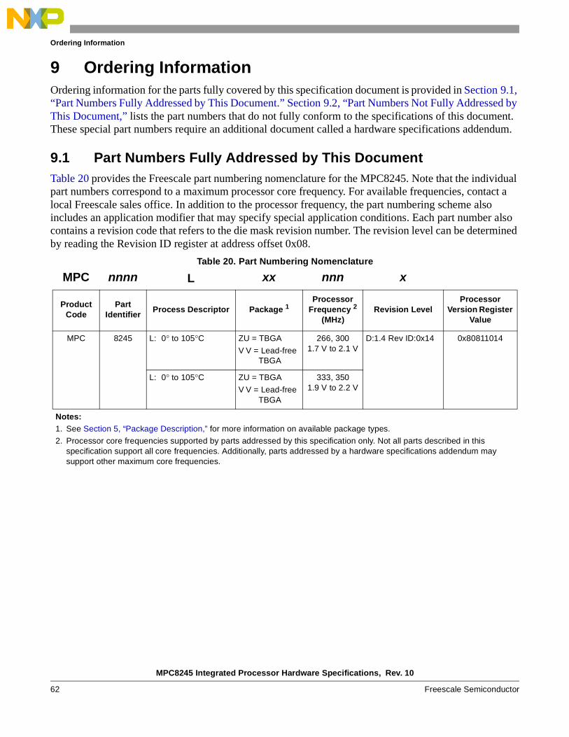
MPC8245 Integrated Processor Hardware Specifications, Rev. 10
62 Freescale Semiconductor
Ordering Information
9 Ordering InformationOrdering information for the parts fully covered by this specification document is provided in Section 9.1, “Part Numbers Fully Addressed by This Document.” Section 9.2, “Part Numbers Not Fully Addressed by This Document,” lists the part numbers that do not fully conform to the specifications of this document. These special part numbers require an additional document called a hardware specifications addendum.
9.1 Part Numbers Fully Addressed by This DocumentTable 20 provides the Freescale part numbering nomenclature for the MPC8245. Note that the individual part numbers correspond to a maximum processor core frequency. For available frequencies, contact a local Freescale sales office. In addition to the processor frequency, the part numbering scheme also includes an application modifier that may specify special application conditions. Each part number also contains a revision code that refers to the die mask revision number. The revision level can be determined by reading the Revision ID register at address offset 0x08.
Table 20. Part Numbering Nomenclature
MPC nnnn L xx nnn x
Product Code
Part Identifier
Process Descriptor Package 1Processor
Frequency 2
(MHz)Revision Level
Processor Version Register
Value
MPC 8245 L: 0° to 105°C ZU = TBGA
V V = Lead-free TBGA
266, 3001.7 V to 2.1 V
D:1.4 Rev ID:0x14 0x80811014
L: 0° to 105°C ZU = TBGA
V V = Lead-free TBGA
333, 3501.9 V to 2.2 V
Notes: 1. See Section 5, “Package Description,” for more information on available package types.
2. Processor core frequencies supported by parts addressed by this specification only. Not all parts described in this specification support all core frequencies. Additionally, parts addressed by a hardware specifications addendum may support other maximum core frequencies.
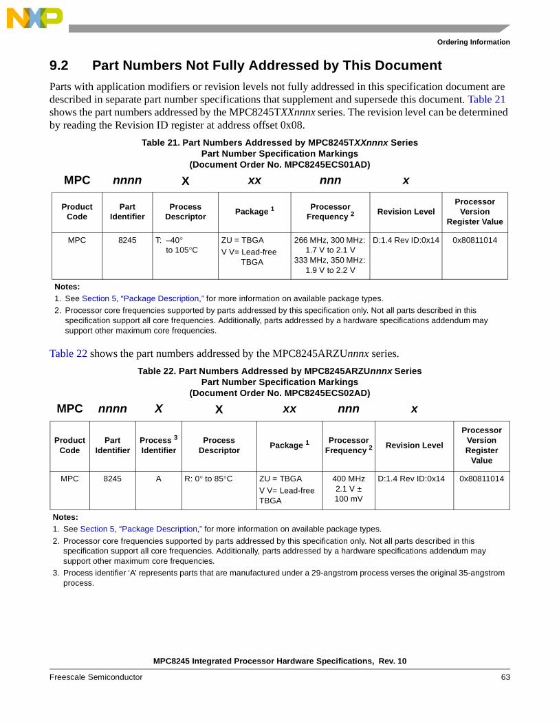
MPC8245 Integrated Processor Hardware Specifications, Rev. 10
Freescale Semiconductor 63
Ordering Information
9.2 Part Numbers Not Fully Addressed by This DocumentParts with application modifiers or revision levels not fully addressed in this specification document are described in separate part number specifications that supplement and supersede this document. Table 21 shows the part numbers addressed by the MPC8245TXXnnnx series. The revision level can be determined by reading the Revision ID register at address offset 0x08.
Table 22 shows the part numbers addressed by the MPC8245ARZUnnnx series.
Table 21. Part Numbers Addressed by MPC8245TXXnnnx Series Part Number Specification Markings
(Document Order No. MPC8245ECS01AD)
MPC nnnn X xx nnn x
Product Code
Part Identifier
Process Descriptor
Package 1 Processor Frequency 2
Revision LevelProcessor
Version Register Value
MPC 8245 T: –40° to 105°C
ZU = TBGA
V V= Lead-free TBGA
266 MHz, 300 MHz: 1.7 V to 2.1 V
333 MHz, 350 MHz: 1.9 V to 2.2 V
D:1.4 Rev ID:0x14 0x80811014
Notes: 1. See Section 5, “Package Description,” for more information on available package types.
2. Processor core frequencies supported by parts addressed by this specification only. Not all parts described in this specification support all core frequencies. Additionally, parts addressed by a hardware specifications addendum may support other maximum core frequencies.
Table 22. Part Numbers Addressed by MPC8245ARZUnnnx Series Part Number Specification Markings
(Document Order No. MPC8245ECS02AD)
MPC nnnn X X xx nnn x
Product Code
Part Identifier
Process 3
IdentifierProcess
DescriptorPackage 1
Processor Frequency 2
Revision Level
Processor Version Register
Value
MPC 8245 A R: 0° to 85°C ZU = TBGA
V V= Lead-free TBGA
400 MHz2.1 V ± 100 mV
D:1.4 Rev ID:0x14 0x80811014
Notes: 1. See Section 5, “Package Description,” for more information on available package types.
2. Processor core frequencies supported by parts addressed by this specification only. Not all parts described in this specification support all core frequencies. Additionally, parts addressed by a hardware specifications addendum may support other maximum core frequencies.
3. Process identifier ‘A’ represents parts that are manufactured under a 29-angstrom process verses the original 35-angstrom process.
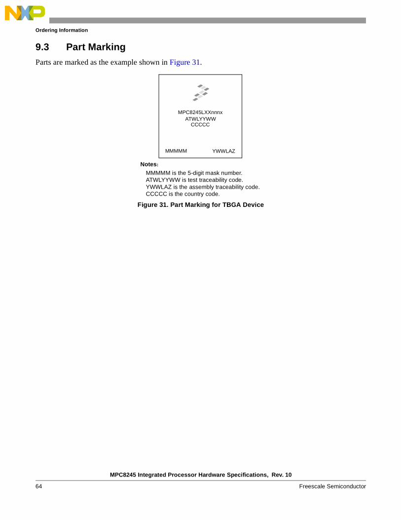
MPC8245 Integrated Processor Hardware Specifications, Rev. 10
64 Freescale Semiconductor
Ordering Information
9.3 Part MarkingParts are marked as the example shown in Figure 31.
Figure 31. Part Marking for TBGA Device
Notes:
MMMMM is the 5-digit mask number.ATWLYYWW is test traceability code.
MPC8245LXXnnnx
MMMMM
ATWLYYWWCCCCC
YWWLAZ
YWWLAZ is the assembly traceability code.CCCCC is the country code.

MPC8245 Integrated Processor Hardware Specifications, Rev. 10
Freescale Semiconductor 65
Ordering Information
THIS PAGE INTENTIONALLY LEFT BLANK
MPC8245 Integrated Processor Hardware Specifications, Rev. 10
66 Freescale Semiconductor
Ordering Information
THIS PAGE INTENTIONALLY LEFT BLANK
MPC8245 Integrated Processor Hardware Specifications, Rev. 10
Freescale Semiconductor 67
Ordering Information
THIS PAGE INTENTIONALLY LEFT BLANK
Document Number: MPC8245ECRev. 1008/2007
Information in this document is provided solely to enable system and software
implementers to use Freescale Semiconductor products. There are no express or
implied copyright licenses granted hereunder to design or fabricate any integrated
circuits or integrated circuits based on the information in this document.
Freescale Semiconductor reserves the right to make changes without further notice to
any products herein. Freescale Semiconductor makes no warranty, representation or
guarantee regarding the suitability of its products for any particular purpose, nor does
Freescale Semiconductor assume any liability arising out of the application or use of
any product or circuit, and specifically disclaims any and all liability, including without
limitation consequential or incidental damages. “Typical” parameters which may be
provided in Freescale Semiconductor data sheets and/or specifications can and do
vary in different applications and actual performance may vary over time. All operating
parameters, including “Typicals” must be validated for each customer application by
customer’s technical experts. Freescale Semiconductor does not convey any license
under its patent rights nor the rights of others. Freescale Semiconductor products are
not designed, intended, or authorized for use as components in systems intended for
surgical implant into the body, or other applications intended to support or sustain life,
or for any other application in which the failure of the Freescale Semiconductor product
could create a situation where personal injury or death may occur. Should Buyer
purchase or use Freescale Semiconductor products for any such unintended or
unauthorized application, Buyer shall indemnify and hold Freescale Semiconductor
and its officers, employees, subsidiaries, affiliates, and distributors harmless against all
claims, costs, damages, and expenses, and reasonable attorney fees arising out of,
directly or indirectly, any claim of personal injury or death associated with such
unintended or unauthorized use, even if such claim alleges that Freescale
Semiconductor was negligent regarding the design or manufacture of the part.
How to Reach Us:
Home Page: www.freescale.com
Web Support: http://www.freescale.com/support
USA/Europe or Locations Not Listed: Freescale Semiconductor, Inc.Technical Information Center, EL5162100 East Elliot Road Tempe, Arizona 85284 +1-800-521-6274 or+1-480-768-2130www.freescale.com/support
Europe, Middle East, and Africa:Freescale Halbleiter Deutschland GmbHTechnical Information CenterSchatzbogen 781829 Muenchen, Germany+44 1296 380 456 (English) +46 8 52200080 (English)+49 89 92103 559 (German)+33 1 69 35 48 48 (French) www.freescale.com/support
Japan: Freescale Semiconductor Japan Ltd. HeadquartersARCO Tower 15F1-8-1, Shimo-Meguro, Meguro-ku Tokyo 153-0064Japan 0120 191014 or+81 3 5437 [email protected]
Asia/Pacific: Freescale Semiconductor Hong Kong Ltd. Technical Information Center2 Dai King Street Tai Po Industrial Estate Tai Po, N.T., Hong Kong +800 2666 [email protected]
For Literature Requests Only:Freescale Semiconductor
Literature Distribution Center P.O. Box 5405Denver, Colorado 80217 +1-800 441-2447 or+1-303-675-2140Fax: +1-303-675-2150LDCForFreescaleSemiconductor
@hibbertgroup.com
Freescale™ and the Freescale logo are trademarks of Freescale Semiconductor, Inc. The Power Architecture and Power.org word marks and the Power and Power.org logos and related marks are trademarks and service marks licensed by Power.org. The described product contains a PowerPC processor core. The PowerPC name is a trademark of IBM Corp. and used under license. IEEE 1149.1 is a registered trademark of the Institute of Electrical and Electronics Engineers, Inc. (IEEE). This product is not endorsed or approved by the IEEE. TUNDRA, the Tundra logo, Tsi107, and Silicon Behind the Network are all trademarks of Tundra Semiconductor Corporation. All other product or service names are the property of their respective owners.
© Freescale Semiconductor, Inc., 2001–2007. All rights reserved.