Embed Size (px)
Citation preview

Freescale Semiconductor32-Bit Embedded Controller Division
MPC5567 RevA Errata List July 31, 2007
Blocks affected
BAM - Boot Assist Module DSPI - Deserial Serial Peripheral Interface EBI - External Bus Interface FEC - Fast Ethernet Controller FLASH - Flash array and Control FMPLL - Frequency Modulated Phase-Locked Loop FlexCAN - Controller Area Network Module FlexRay - FlexRay Communication Module MPC5567 - Overall Device NPC - Nexus Port Controller NZ6C3 - e200z6 Nexus Class 3 Interface Pad Ring - Pad Ring SIU - System Integration Unit SRAM - Static RAM e200z6 - Main Processor Core eDMA - Enhanced Direct Memory Access eMIOS - Enhanced Modular Input/Output Subsystem eQADC - Enhanced Queued Analog to Digital ConvereTPU - Enhanced Time Processor Unit
Report Generated: 31 Jul 2007 Page 1 Freescale Semiconductor
MPC5567 RevA Errata List

Errata and Information SummaryErrata 2297 BAM: Serial download unavailable to last 16 bytes (4 words) of System RAM
Errata 6049 BAM: VLE added to the LENGTH field during serial boot message
Errata 1123 DSPI: Changing CTARs between frames in continuous PCS mode causes error
Errata 4022 DSPI: DSPI_B pins split to separate supply, VDDEH10
Errata 4031 DSPI: DSPI D PCS[3:4] are slow speed pins
Errata 1874 EBI: Additional Address lines available
Errata 2379 EBI: Calibration pads are 1 ns slower than EBI
Errata 2823 EBI: Do not access external resources when the EBI is disabled
Errata 3111 EBI: Dual controller mode cannot be guaranteed under all conditions
Errata 3839 EBI: Timed out accesses (external TA only) may generate spurious TS_B pulse
Errata 741 FEC: slot time is designed for 516 bit times; deviation from the 802.3
Errata 1745FLASH: The ADR register may get loaded with a flash address even through no ECCerror has occurred
Errata 2371 FLASH: Large blocks limited to 1,000 Program/erase cycles
Errata 2419 FLASH: Minimum Programming Frequency is 25 MHz
Errata 715 FMPLL: LOLF can be set on MFD change
Errata 4527 FMPLL: Oscillator Gain Increased
Errata 3138 FlexCAN: New feature - Transmit (TX)/Receive (RX) Warning Interrupts
Errata 3566 FlexCAN: New feature - Self reception disable
Errata 3567 FlexCAN: New feature - Individual RX matching and Message Queuing
Errata 3617 FlexCAN: New Feature - Individual Message Mask Registers
Errata 4414 FlexCAN: Corrupt ID may be sent in early-SOF condition
Errata 5164 FlexCAN: Freeze FlexCAN A to write RXIMR for FlexCAN C
Errata 3657FlexRay: A boundary violation frame followed by a valid startup frame during thestartup phase may cause an abort of the startup
Errata 4128 FlexRay: Slot Status of Double Transmit Message Buffers updated incorrectly
Page 2Report Generated: 31 Jul 2007 Freescale Semiconductor
MPC5567 RevA Errata List
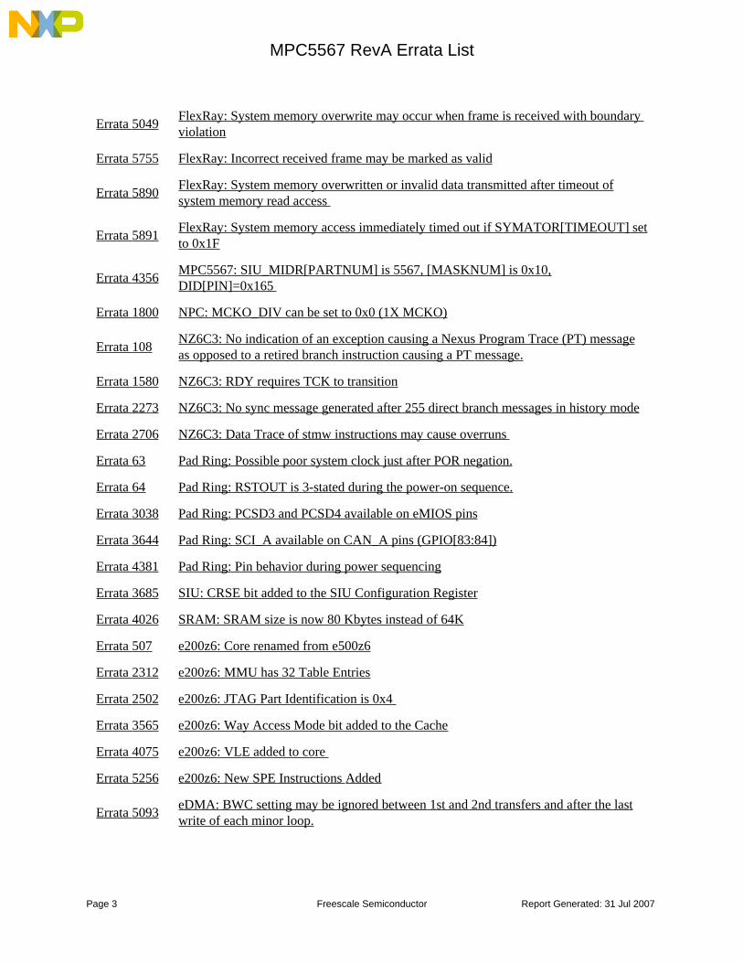
Errata 5049FlexRay: System memory overwrite may occur when frame is received with boundary violation
Errata 5755 FlexRay: Incorrect received frame may be marked as valid
Errata 5890FlexRay: System memory overwritten or invalid data transmitted after timeout ofsystem memory read access
Errata 5891FlexRay: System memory access immediately timed out if SYMATOR[TIMEOUT] setto 0x1F
Errata 4356MPC5567: SIU_MIDR[PARTNUM] is 5567, [MASKNUM] is 0x10,DID[PIN]=0x165
Errata 1800 NPC: MCKO_DIV can be set to 0x0 (1X MCKO)
Errata 108NZ6C3: No indication of an exception causing a Nexus Program Trace (PT) messageas opposed to a retired branch instruction causing a PT message.
Errata 1580 NZ6C3: RDY requires TCK to transition
Errata 2273 NZ6C3: No sync message generated after 255 direct branch messages in history mode
Errata 2706 NZ6C3: Data Trace of stmw instructions may cause overruns
Errata 63 Pad Ring: Possible poor system clock just after POR negation.
Errata 64 Pad Ring: RSTOUT is 3-stated during the power-on sequence.
Errata 3038 Pad Ring: PCSD3 and PCSD4 available on eMIOS pins
Errata 3644 Pad Ring: SCI_A available on CAN_A pins (GPIO[83:84])
Errata 4381 Pad Ring: Pin behavior during power sequencing
Errata 3685 SIU: CRSE bit added to the SIU Configuration Register
Errata 4026 SRAM: SRAM size is now 80 Kbytes instead of 64K
Errata 507 e200z6: Core renamed from e500z6
Errata 2312 e200z6: MMU has 32 Table Entries
Errata 2502 e200z6: JTAG Part Identification is 0x4
Errata 3565 e200z6: Way Access Mode bit added to the Cache
Errata 4075 e200z6: VLE added to core
Errata 5256 e200z6: New SPE Instructions Added
Errata 5093eDMA: BWC setting may be ignored between 1st and 2nd transfers and after the lastwrite of each minor loop.
Report Generated: 31 Jul 2007 Page 3 Freescale Semiconductor
MPC5567 RevA Errata List

Errata 2305 eMIOS: OPMWC unable to produce close to 100% duty cycle signal
Errata 1742 eQADC: 50% reference channels reads 20 mv low
Errata 2878 eQADC: conversions of muxed digital/analog channels close to the rail
Errata 3819 eQADC : 25% calibration channel sampling requires at least 64 sampling cycles
Errata 2477 eTPU: MISSCNT can fail on sequential physical teeth
Errata 3150 eTPU: STAC bus export may skip 1 count
Page 4Report Generated: 31 Jul 2007 Freescale Semiconductor
MPC5567 RevA Errata List
Errata and Information Details
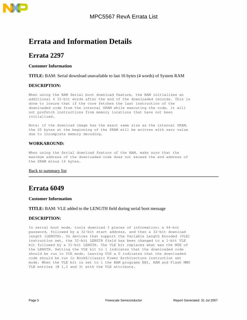
Errata 2297Customer Information
TITLE: BAM: Serial download unavailable to last 16 bytes (4 words) of System RAM
DESCRIPTION:
When using the BAM Serial boot download feature, the BAM initializes anadditional 4 32-bit words after the end of the downloaded records. This isdone to insure that if the core fetches the last instruction of thedownloaded code from the internal SRAM while executing the code, it willnot prefetch instructions from memory locations that have not beeninitialized.
Note: if the download image has the exact same size as the internal SRAM,the 20 bytes at the beginning of the SRAM will be written with zero valuedue to incomplete memory decoding.
WORKAROUND:
When using the Serial download feature of the BAM, make sure that themaximum address of the downloaded code does not exceed the end address ofthe SRAM minus 16 bytes.
Back to summary list
Errata 6049Customer Information
TITLE: BAM: VLE added to the LENGTH field during serial boot message
DESCRIPTION:
In serial boot mode, tools download 3 pieces of information: a 64-bitpassword, followed by a 32-bit start address, and then a 32-bit downloadlength (LENGTH). On devices that support the Variable Length Encoded (VLE)instruction set, the 32-bit LENGTH field has been changed to a 1-bit VLEbit followed by a 31-bit LENGTH. The VLE bit replaces what was the MSB ofthe LENGTH. Setting the VLE bit to 1 indicates that the downloaded codeshould be run in VLE mode. Leaving VLE a 0 indicates that the downloadedcode should be run in BookE/classic Power Architecture instruction setmode. When the VLE bit is set to 1 the BAM programs EBI, RAM and Flash MMUTLB entries (# 1,2 and 3) with the VLE attribute.
Report Generated: 31 Jul 2007 Page 5 Freescale Semiconductor
MPC5567 RevA Errata List

WORKAROUND:
Set the VLE bit (MSB of the 32-bit LENGTH) in the serial boot download dataif the code being downloaded uses (was written in) VLE instructions.
Back to summary list
Errata 1123Customer Errata
TITLE: DSPI: Changing CTARs between frames in continuous PCS mode causes error
DESCRIPTION:
Erroneous data could be transmitted if multiple Clock and TransferAttribute Registers (CTAR) are used while using the Continuous PeripheralChip Select mode (DSPIx_PUSHR[CONT=1]). The conditions that can generate anerror are:
1) If DSPIx_CTARn[CPHA]=1 and DSPIx_MCR[CONT_SCKE = 0] andDSPIx_CTARn[CPOL, CPHA, PCSSCK or PBR] change between between frames.
2) If DSPIx_CTARn[CPHA]=0 or DSPIx_MCR[CONT_SCKE = 1] and any bit field ofDSPIx_CTARn changes between frames except DSPIx_CTARn[PBR].
WORKAROUND:
When generating DSPI bit frames in continuous PCS mode, adhere to theaforementioned conditions when changing DSPIx_CTARn bit fields betweenframes.
Back to summary list
Errata 4022Customer Information
TITLE: DSPI: DSPI_B pins split to separate supply, VDDEH10
DESCRIPTION:
The DSPI_B SINB, SOUTB, SCKB, PCS_B[0:2] were separated from the VDDEH6 andare now powered by the new power supply pin VDDEH10. Ball J23 on the 416package was changed from being a duplicate VDDEH6 pin to being a separateVDDEH10 supply pin. 324 pin package drawings show the VDDE10 ballplacement. VDDEH6 and VDDEH10 are combined/shorted internally on 208packages.
Page 6Report Generated: 31 Jul 2007 Freescale Semiconductor
MPC5567 RevA Errata List

WORKAROUND:
For compatibility to the MPC5554, always power VDDEH6 and VDDEH10 from thesame power supply (3.0 to 5.25 volts). If compatibility is not required tothe MPC5554, VDDEH10 and VDDEH6 can be supplied by different voltagesupplies. This allows one DSPI to operate at a different voltage than theother DSPI modules (3.3 and 5 volts, for example).
Back to summary list
Errata 4031Customer Information
TITLE: DSPI: DSPI D PCS[3:4] are slow speed pins
DESCRIPTION:
The eMIOS[10:11]/PCSD[3:4]/GPIO[189:190] pins have a pad type of SH (slowspeed pad) instead of MH (medium speed pad). While the eMIOS functionnormally does not require a medium speed pad, when the pin is configured asthe Deserial Serial Peripheral Interface D Peripheral Chip Select(DSPI_PCSxD), the slow pad may limit the maximum speed of the DSPI port.
WORKAROUND:
Either don’t use the DSPI_D PCS functions on these pins or limit thefrequency of the DSPI port to account for the difference in slew rate ofthe pins. The slow pads have a slew rate of 15 to 200 ns and the mediumspeed pads have a slew rate of 8 to 100 ns (both with a 50 pF load)depending on the setting of the Slew Rate Control bits in the PadConfiguration register (PCRx[SRC]).
Back to summary list
Errata 1874Customer Information
TITLE: EBI: Additional Address lines available
DESCRIPTION:
Two additional address lines (ADDR6 and ADDR7) have been added to theExternal Bus Interface (EBI). These extra address lines are multiplexedwith ADDR30 and ADDR31 as alternate functions and can be selected by thePin Assignment (PA) field of SIU_PCR[26] and SIU_PCR[27].
Report Generated: 31 Jul 2007 Page 7 Freescale Semiconductor
MPC5567 RevA Errata List

WORKAROUND:
Customers should be aware that not all members of the MPC5500 family withan external address bus have these extra 2 address lines.
Note external masters still use ADDR30 and ADDR31 for internal accesses andalways use ADDR8 though ADDR31 in this case.
Back to summary list
Errata 2379Customer Information
TITLE: EBI: Calibration pads are 1 ns slower than EBI
DESCRIPTION:
The calibration bus outputs and input setup time is 1ns longer than theequivalent normal External bus signals. Therefore, the electricalspecifications need to be added to the data sheets for the calibrationsignals.
WORKAROUND:
For synchronous (to CLKOUT) peripherals on the calibration pads, makecertain that the bus will meet the new electrical specification.
Back to summary list
Errata 2823Customer Information
TITLE: EBI: Do not access external resources when the EBI is disabled
DESCRIPTION:
When the external bus is disabled in the External Bus Interface ModuleControl Register (EBI_MCR[MDIS] = 1), accesses through the EBI will notterminate and the master requesting the access will not request anotherone.
WORKAROUND:
Do not disable the EBI or do not allow accesses to the external bus throughMemory Management Unit (MMU) settings in the core. Other internal busmasters (such as DMA) bypasses the MMU and therefore these accesses willhang the external bus if the destination is in the external bus addressmap.
Page 8Report Generated: 31 Jul 2007 Freescale Semiconductor
MPC5567 RevA Errata List
Back to summary list
Errata 3111Customer Errata
TITLE: EBI: Dual controller mode cannot be guaranteed under all conditions
DESCRIPTION:
In dual controller mode, the specification for the phase relationshipbetween EXTAL and CLKOUT is +/- 1 ns, however this does not allow adequateset up and hold times to guarantee successful operation of the external busto a second MCU.
WORKAROUND:
Do not use in Dual Controller mode.
Back to summary list
Errata 3839Customer Errata
TITLE: EBI: Timed out accesses (external TA only) may generate spurious TS_B pulse
DESCRIPTION:
When an external Transfer Acknowledge (TA) access times out, there is aboundary case where the External Bus Interface (EBI) asserts a TransferStart (TS) pulse as if starting another access, even if no other internalrequest is pending. The boundary case is when the access is part of a"small access" set (sequence of external accesses to satisfy 1 internalrequest), and when the external TA arrives around the same cycle (+/- 1clkout cycle) as the bus monitor timeout (BMT).
Most EBI signals will stay negated during this erroneous transfer (CS, OE,WE, BDIP). However, along with TS assertion, RD_WR may also assert (for 1cycle only, during this phantom TS), if the prior access that timed out wasa write. This condition can generate an erroneous write transfer (with CSnegated). The address (ADDR pins) will be incremented to the address of thenext small access transfer that would have been performed, and the valuedriven by the EBI on the DATA bus (if a write) may change. Busy Busy (BB)may be asserted along with the phantom TS (if external master modes isenabled in the EBI Module configuration Register, SIU_MCR[EXTM]=1), and theTransfer Size (TSIZ) value may change.
Internally, the EBI terminates the timeout access, and the internal statemachine goes to IDLE after the timeout access. So the EBI will not be
Report Generated: 31 Jul 2007 Page 9 Freescale Semiconductor
MPC5567 RevA Errata List

"hung" after the spurious TS, and the EBI does respond properly to futureinternal or external requests.
However, the side effect of the spurious TS is that it may cause anexternal non-chip-select device to think an access is being performed toit, resulting in 1 of 2 bad effects (depending on RD_WR value duringspurious TS):
1) RD_WR high (read): ext. device may drive back read data some number ofcycles later, possibly conflicting with a future real access (e.g. write)that might have started by that time.
2) RD_WR low (write): ext. device may get an erroneous write performed toit
Note that the soonest possible TS for a real transfer (after the timeouttransfer), is 2 cycles after the spurious TS (so 1 cycle gap), meaning thisBug will never result in a 2-cycle TS pulse.
WORKAROUND:
Do not enable bus monitor in the EBI Bus Monitor Control Register (keepSIU_BMCR[BME]=0), unless at least 1 of the following 3 conditions can bemet:
1) The external TA will never be asserted from external device within 1cycle of when the access would be timing out (see NOTE below)
2) No internal requests greater than external bus size will be performed(e.g. doing data-only fetches of 32 bits or less on 32-bit data bus or 16bits or less on a 16 bit bus only, so a "small access" could never occur).
3) The side effect of this TS pulse driven to non-CS device is judged to betolerable in system after a timeout error occurs; depends on spec ofexternal device and user requirements for data coherency after a timeouterror occurs.
NOTE: Of the 3 above, #1 is easiest to achieve in most systems. If themaximum possible TA latency of the external device is known, the user justneeds to set the BMT period more than (external device maximum latency +2), and this condition will not occur.
Back to summary list
Errata 741Customer Information
TITLE: FEC: slot time is designed for 516 bit times; deviation from the 802.3
DESCRIPTION:
Page 10Report Generated: 31 Jul 2007 Freescale Semiconductor
MPC5567 RevA Errata List
The Fast Ethernet Controller (FEC) slot time is 516 bit times which islonger than the 512 bit times specified by the IEEE 802.3 standard.
If a collision occurs after the standard 512 bit times (but prior to 516bit times), the FEC may generate a retry that a remote ethernet device mayidentify as late. In addition, the slot time is used as an input to thebackoff timer, therefore the FEC retry timing could be longer thanexpected.
WORKAROUND:
No software workaround is needed or available.
Back to summary list
Errata 1745Customer Information
TITLE: FLASH: The ADR register may get loaded with a flash address even through no ECC error has occurred
DESCRIPTION:
The Flash Address Register (FLASH_AR) may be loaded with a flash addresswhen no Error Correction Code (ECC) has occurred. When an ECC does occur,the FLASH_AR is properly set.
WORKAROUND:
Check the Flash Module Control Register ECC Event Error (FLASH_MCR[EER]=1)to check for an ECC error before examining the ADR register. If an errorhas occurred then the ADR register data is valid. If an error has notoccurred then the FLASH_AR data could change on any flash access.
Back to summary list
Errata 2371Customer Errata
TITLE: FLASH: Large blocks limited to 1,000 Program/erase cycles
DESCRIPTION:
Report Generated: 31 Jul 2007 Page 11 Freescale Semiconductor
MPC5567 RevA Errata List

The electrical specification for Program/Erase cycling on large Flashblocks (all 128K blocks - Middle Address Space [MAS] blocks M0 and M1, plusHigh Address Space [HAS] blocks H0 to H3/H7/H11/H19 [depending on totalflash size]) has been changed to 1,000 PE cycles minimum. The small blocks(16K, 48K, and 64K - Low Address Space [LAS] blocks L0-L5) are stillspecified as 100,000 PE cycles minimum.
The data retention specification all blocks is still 20 years for blockscycled less than 1000 times and 5 years for blocks cycled 1001 to 100,000cycles (1,000 for large blocks).
WORKAROUND:
Only use the small blocks for EEPROM emulation (LAS L0-L5). Do not useblocks MAS M0/M1 or HAS H0 to H3/H7/H11/H19 (depending on total flash size)for EEPROM emulation requiring greater than 1,000 Program/Erase cycles.Refer to the latest device electrical specifications (Data Sheet) datedJuly 2007 or later.
Back to summary list
Errata 2419Customer Information
TITLE: FLASH: Minimum Programming Frequency is 25 MHz
DESCRIPTION:
Programming and erase operations of the internal flash could fail if theclock to the flash (usually the system clock) is less than 25 MHz.
WORKAROUND:
Do not program or erase the flash when the system operating frequency isbelow 25Mhz.
Back to summary list
Errata 715Customer Errata
TITLE: FMPLL: LOLF can be set on MFD change
DESCRIPTION:
Page 12Report Generated: 31 Jul 2007 Freescale Semiconductor
MPC5567 RevA Errata List

Normally, the Loss of Lock Flag (FMPLL_SYNCR[LOLF]) would not be set if theloss of lock occurred due to changing of the Multiplication Factor Dividerbits or PREDIV bits (FMPLL_SYNCR[MFD] or [PREDIV]) or enabling of FrequencyModulation (FMPLL_SYNCR[Depth]>0b00). However, if LOLF has been setpreviously (due to an unexpected loss of lock condition) and then cleared(by writing a 1), a change of the MFD, PREDIV or DEPTH fields can cause theLOLF to be set again which can trigger an interrupt request if LOLIRQ bitis set.
In addition, changing the RATE bit will also set the LOLF regardless ofprevious conditions.
WORKAROUND:
The Loss of Lock Interrupt Request enable in the Synthesizer ControlRegister (FMPLL_SYNCR[LOLIRQ]) should be cleared before any change to themultiplication factor (MFD), PREDIV, modulation depth (DEPTH), ormodulation rate (RATE) to avoid unintentional interrupt requests. After thePLL has locked (LOCK=1), LOLF should be cleared (by writing a 1) and LOLIRQmay be set again if required.
Back to summary list
Errata 4527Customer Information
TITLE: FMPLL: Oscillator Gain Increased
DESCRIPTION:
The gain of the oscillator was increased to handle a 40 MHz crystal on somedevices. The 40 MHz crystal, however, is not supported on all devices.
WORKAROUND:
A resistor may need to be added between the XTAL pin and the crystal.Consult the crystal manufacturer for the recommended crystal configuration,however, 2.7K ohms is a good starting point for an 8 MHz crystal and a 470ohms for a 40 MHz crystal.
Back to summary list
Errata 3138Customer Information
TITLE: FlexCAN: New feature - Transmit (TX)/Receive (RX) Warning Interrupts
Report Generated: 31 Jul 2007 Page 13 Freescale Semiconductor
MPC5567 RevA Errata List

DESCRIPTION:
The Warning Interrupt bit has been added in the FlexCAN ModuleConfiguration Register, CANx_MCR[WRNEN] (bit 10). In addition two bits havebeen added in the FlexCAN Control Register, Transmit Warning InterruptMask, CANx_CR[TWRNMSK] (bit 20)and the Receive Warning Mask,CANx_CTRL[RWRNMSK] (bit 21) allow applications to enable monitoring forTransmit and Receive error counters and generate an interrupt for either ifthe error count reaches 96 errors or more. Consequently, two status bitshave been added in the FlexCAN Error and Status register to signalinterrupts for these additional interrupt causes, the Transmit WarningInterrupt bit (CANx_ESR[TWRNINT], bit 14) and the Receive Warning Interruptbit (CANx_ESR[RWRNINT], bit 15). Both of these status bits are cleared bywriting a 1 to the bit.
WORKAROUND:
For backwards software compatibility with the MPC5554, MPC5553, and theinitial versions of the MPC5534, do not use this new feature or insure thatthe feature exists prior to their use.
Back to summary list
Errata 3566Customer Information
TITLE: FlexCAN: New feature - Self reception disable
DESCRIPTION:
The FlexCAN can now be configured to disallow reception of framestransmitted by itself by setting the Self Reception Disable bit in theFlexCAN Module Configuration Register (CANx_MCR[SRXDIS]=0b1, bit 14).
WORKAROUND:
For backwards software compatibility with the MPC5554, MPC5553, and theinitial versions of the MPC5534, do not use these new features or insurethat the features exist prior to their use.
Back to summary list
Errata 3567Customer Information
Page 14Report Generated: 31 Jul 2007 Freescale Semiconductor
MPC5567 RevA Errata List

TITLE: FlexCAN: New feature - Individual RX matching and Message Queuing
DESCRIPTION:
The FlexCAN allows reception of the same message ID in multiple messagebuffers by setting the new Message Buffer Filter Enable control bit in theFlexCAN Module Configuration Register, CANx_MCR[MBFEN] (bit 15). Byprogramming more than one Message Buffer with the same ID or using a mask,received messages will be queued into the Message Buffers.
WORKAROUND:
For backwards software compatibility with the MPC5554, MPC5553, and theinitial versions of the MPC5534, do not use this new feature or insure thatthe feature exists prior to their use.
Back to summary list
Errata 3617Customer Information
TITLE: FlexCAN: New Feature - Individual Message Mask Registers
DESCRIPTION:
When the FlexCAN Message Buffer Filter Enable control bit in the FlexCANModule Configuration Register, CANx_MCR[MBFEN] (bit 15), is set, additional filtering is provided by the RXIMR0 to RXIMR63 Individual MaskRegisters which replace RXGMASK, RX14MASK and RX15MASK.
WORKAROUND:
This feature may not exist on all parts, and for software compatibilitywith devices that do not include Individual message mask registers, do notuse the additional message mask registers. They can be used if backwardssoftware compatibility is not required.
Back to summary list
Errata 4414Customer Information
TITLE: FlexCAN: Corrupt ID may be sent in early-SOF condition
DESCRIPTION:
Report Generated: 31 Jul 2007 Page 15 Freescale Semiconductor
MPC5567 RevA Errata List

This erratum is not relevant in a typical CAN network, with oscillatortolerances inside the specified limits, because an early start of framecondition (early-SOF) should not occur.
An early-SOF may only be a problem if the oscillators in the networkoperate at opposite ends of the tolerance range (maximum 1.58%), whichcould lead to a cumulated phase error after 10 bit-times larger than phasesegment 2.
A corrupt ID will be sent out if a transmit message buffer is identifiedfor transmission during INTERMISSION, and an early-SOF condition is entereddue to a dominant bit being sampled during bit 3 of INTERMISSION.
The message sent will be taken from the newly set up transmit buffer (TxMB), with the exception of the 1st 8 ID bits, which are taken from thepreviously selected Tx MB.
The CRC is correctly calculated on the resulting bit stream so thatreceiving nodes will validate the message.
The early-SOF condition is detailed in the Bosch CAN Specification Version2.0 Part B, Section 3.2.5 INTERFRAME SPACING - INTERMISSION.
WORKAROUND:
1) Configure Tx MBs during FREEZE mode, or2) Out of FREEZE mode, configure Tx MBs during bus idle:- For networks with low traffic, determine Bus Idle status by reading theIdle bit of the Error and Status register (CANx_ESR[IDLE]).
- For networks with high traffic, configure Tx MBs after the 3rd bit ofintermission, and before the third bit of the CRC field from the nexttransmission.
Back to summary list
Errata 5164Customer Errata
TITLE: FlexCAN: Freeze FlexCAN A to write RXIMR for FlexCAN C
DESCRIPTION:
The individual receive mask registers for FlexCAN C (CANC_RXIMR0 -CANC_RXIMR63) cannot be written unless FlexCAN A is in freeze mode. Writingvalues to these registers is ignored unless FlexCAN A is also in freezemode. Reading of these registers is not affected by FlexCAN A.
WORKAROUND:
Page 16Report Generated: 31 Jul 2007 Freescale Semiconductor
MPC5567 RevA Errata List
To write the individual receive mask registers for FlexCAN C (CANC_RXIMRx),place FlexCAN A into freeze mode as well as follow the documented rules forwriting these registers i.e. FlexCAN C must be in freeze mode and itsmessage buffer filter enable must be set in the CAN Module ConfigurationRegister, i.e. CANC_MCR[MBFEN] should be 1.
Back to summary list
Errata 3657Customer Errata
TITLE: FlexRay: A boundary violation frame followed by a valid startup frame during the startup phasemay cause an abort of the startup
DESCRIPTION:
The FlexRay module may abort the startup due to a wrong deviationmeasurement if:
(a) The FlexRay module is in STARTUP state and(b) the FlexRay module receives a startup frame that violates the boundaryat the beginning of the slot followed by a valid startup frame in the sameslot.
The following flags and fields may be affected:
(a) The PROTSTATE field of the Protocol Status Register FR_PSR0 mayindicate INTEGRATION_LISTEN instead of NORMAL_ACTIVE after the startup.(b) The OFFSETCORR field in the Offset Correction Value Register(FR_OFCORVR) may show a wrong value for the related communication cycle.(c) The RATECORR field in the Rate Correction Value Register (FR_RTCORVR)may show a wrong value for the related communication cycle pair.(d) The Clock Correction Limit Reached Interrupt Flag CCL_IF of theProtocol Interrupt Flag Register 0 (FR_PIFR0) may be set by the FlexRaymodule, indicating an EXCEED_BOUNDS condition due to the erroneousdeviation measurement.
WORKAROUND:
There is no workaround for this erratum.
Back to summary list
Errata 4128Customer Errata
Report Generated: 31 Jul 2007 Page 17 Freescale Semiconductor
MPC5567 RevA Errata List

TITLE: FlexRay: Slot Status of Double Transmit Message Buffers updated incorrectly
DESCRIPTION:
This erratum only affects FlexRay modules that have at least two doubletransmit message buffers configured by the application.
After the transmission of a non-null frame from a double transmit messagebuffer, the FlexRay module
1) updates the slot status of the transmit side of this double transmitmessage buffer,2) does not update the slot status of the commit side of this doubletransmit message buffer, and3) updates the slot status of the commit side of the double transmitmessage buffer with the highest message buffer ID.
Due to internal commit operations on double transmit message buffers it canhappen, that the slot status of the commit side and transmit side areexchanged after the update. As a result, the slot status of the doubletransmit message buffer is incorrect for a certain amount of time.
WORKAROUND:
If the application has configured at most one double transmit messagebuffer, the slot status of this message buffer is always correct.
If the application has configured more than one double transmit messagebuffers, it should ignore the slot status of the double transmit messagebuffers and instead should use the dedicated slot status reportingregisters provided by the FlexRay module to get the slot statusinformation. These registers are- Channel A Status Error Counter Register (FR_CASERCR)- Channel B Status Error Counter Register (FR_CBSERCR)- Protocol Status Register 2 (FR_PSR2)- Protocol Status Register 3 (FR_PSR3)- Slot Status Registers (FR_SSR0 up to FR_SSR7)- Slot Status Counter Registers (FR_SSCR0 up to FR_SSCR3)
Back to summary list
Errata 5049Customer Errata
TITLE: FlexRay: System memory overwrite may occur when frame is received with boundary violation
DESCRIPTION:
When the FlexRay module receives a non-null frame which overlaps the end ofa slot or segment, it may write an undetermined 16-bit data item to anunintended address in the Message Buffers Header and Message Buffer Dataarea in the system memory under one of the following circumstances :
Page 18Report Generated: 31 Jul 2007 Freescale Semiconductor
MPC5567 RevA Errata List

a) the received frame overlaps the end of the static segment, and the laststatic slot is subscribed for reception, and a dynamic segment isconfigured, and the first dynamic slot is not subscribed for reception ortransmission. b) the received frame overlaps the end of the static segment, and the laststatic slot is subscribed for reception, and no dynamic segment isconfigured, c) the received frame overlaps the end of the dynamic segment, and at leastone slot in the dynamic segment is subscribed for reception. This erroneouswrite operation may corrupt the Data Field Offset in the Message BufferHeader Field. The FlexRay module will use this Data Field Offset todetermine the address to store or fetch frame payload data. If the Data Field Offset was corrupted, payload data are written to andread from an unpredictable location within a 64 KByte system memory windowstarting at the address defined by the System Memory Base Address Registers(SYMBADHR,SYMBADLR). As a consequence, in case of a subsequent reception,the content of any location within this 64 KByte window can be corruptedand, in case of a subsequent transmission, incorrect messages can betransmitted. Additionally, when the FlexRay module receives a non-null frame whichoverlaps the end of slot, it may write to both receive shadow buffers, evenif a message buffer segment is not used for reception at all.
WORKAROUND:
The reception of an frame which overlaps the end of a slot or segment isindicated by the aggregated boundary violation flags ABVB/ABVB in theProtocol Status Register 3 (PSR3). To avoid the error situation a) the application should either 1) configure a receive message buffer for the first slot in the dynamicsegment without any cycle counter filtering, or 2) not configure a receive message buffer or receive FIFO for the last slotin the static segment. To avoid the error situation b) the application should not configure areceive message buffer or receive FIFO for the last slot in the staticsegment. To avoid the error situation c) the application should not configure areceive message buffer or receive FIFO for the dynamic segment. If all three error situations can not be avoided, the application should 1) locate the Message Buffer Header Fields for all transmit message buffersbefore (at lower addresses in Internal SRAM) those of the receive messagebuffers, and 2) reserve 244 bytes of unused Internal SRAM space after the last MessageBuffer Header Field, and 3) observe the Boundary Violation flags PSR3[ABVA] and PSR3[ABVB]. In caseof a boundary violation, the application should stop the FlexRay module bythe protocol command FREEZE and then reconfigure the message buffer headerfields of the receive message buffers and reconfigure the receive shadowbuffers. To avoid an undetermined write access to a non-configured receive shadowbuffer, the application should configure the receive shadow buffers for allused message buffer segments even if a segment is used only fortransmission.
Report Generated: 31 Jul 2007 Page 19 Freescale Semiconductor
MPC5567 RevA Errata List

Back to summary list
Errata 5755Customer Errata
TITLE: FlexRay: Incorrect received frame may be marked as valid
DESCRIPTION:
When the FlexRay module has received a frame in the static slot n whichoverlaps the end of slot n, then a valid frame received in the followingslot n+1 may be stored incorrectly. In this case, the content of the FrameHeader in the Message Buffer Header Field and Frame Data in the MessageBuffer Data Field of the message buffer subscribed to slot n+1 may beincorrect.
If a receive message buffer is subscribed to slot n+1, the valid frame bitsVFB/VFA in the Slot Status Field and the Data Updated bit DUP in theMessage Buffer Configuration, Control, Status Registers (MBCCSRn) will beset.
If the receive FIFO is subscribed to slot n+1, the Receive FIFO Not Emptyinterrupt flag FNEAIF/FNEBIF in the Global Interrupt Flag and EnableRegister is set and an additional message is put in the receive FIFO.
WORKAROUND:
The FlexRay module will set the boundary violation bit BVB/BVA in the SlotStatus Field of the message buffer subscribed to slot n+1, because a framereception is still running at the start of slot n+1. The BVB/BVA flags canbe used to detect the error condition.
The application should not process received frames with the boundaryviolation bit BVA/BVB set in the Slot Status Field of the message buffer.
Back to summary list
Errata 5890Customer Errata
TITLE: FlexRay: System memory overwritten or invalid data transmitted after timeout of systemmemory read access
DESCRIPTION:
Page 20Report Generated: 31 Jul 2007 Freescale Semiconductor
MPC5567 RevA Errata List
When the FlexRay module performs a read operation from the system memoryand the system memory subsystem fails to deliver the requested data withinthe number of system clock cycles configured by the TIMEOUT field in theSystem Memory Timeout Register (SYMATOR), the FlexRay module will proceedits operation with a read value of 0.
If the value to be read was in the Frame Header of the Message BufferHeader Field, an incorrect frame header will be transmitted.
If the value to be read was the Data Offset Field of the Message BufferHeader Field the FlexRay module willa) in case of a transmit slot, fetch the payload data from the start of the64 KByte system memory window starting at the address defined by the SystemMemory Base Address Registers (SYMBADHR,SYMBADLR), and consequentlytransmit incorrect payload data, orb) in case of a receive slot, write the payload data to the start of the 64KByte system memory window starting at the address defined by the SystemMemory Base Address Registers (SYMBADHR,SYMBADLR), and consequentlyoverwrite several Message Buffer Header Fields.
If the value to be read was in the Message Buffer Data Field an incorrectpayload word will be transmitted.
WORKAROUND:
To prevent the occurrence of an system memory timeout, the applicationshould configure the priorities for the system memory bus masters in theCrossbar Switch properly along with an appropriate setting of theSYMATOR[TIMEOUT] field.
To prevent the overwrite of Message Buffer Header Fields, the applicationshould reserve 254 bytes of unused memory at the start of the FlexRayMemory Window.
To prevent the transmission of incorrect payload data, the applicationshould continuously observe or assign an interrupt service routine to theSystem Bus Communication Failure Error Flag SBCF_EF in the CHI Error FlagRegister (CHIERFR). When this flag is set or the interrupt is triggered,the application should stop the FlexRay module by the protocol commandFREEZE.
Back to summary list
Errata 5891Customer Errata
TITLE: FlexRay: System memory access immediately timed out if SYMATOR[TIMEOUT] set to 0x1F
DESCRIPTION:
Report Generated: 31 Jul 2007 Page 21 Freescale Semiconductor
MPC5567 RevA Errata List

If the FlexRay module performs a read or write operation on the systemmemory and the TIMEOUT field in the System Memory Timeout Register(SYMATOR) is set to its maximum value of 0x1F, the FlexRay module willimmediately set the System Bus Communication Failure Error Flag SBCF_EF inthe CHI Error Flag Register (CHIERFR). In case of anread operation, the FlexRay module will proceed its operation and assume aread value of 0.
WORKAROUND:
The application should not write the value of 0x1F to the SYMATOR[TIMEOUT]field.
Back to summary list
Errata 4356Customer Information
TITLE: MPC5567: SIU_MIDR[PARTNUM] is 5567, [MASKNUM] is 0x10, DID[PIN]=0x165
DESCRIPTION:
The part number field in the MCU Identification Register(SIU_MIDR[PARTNUM]) is 0x5567. The initial mask revision number(SIU_MIDR[MASKNUM]) is 0x10. The Part Number Identification field in theNexus Port Controller Device Identification Register/JTAGC Identification(NPC_DID[PIN]) is 0x165 and the (NPC_DID[PRN]=0x1). Note that theNPC_DID[PIN] is the same as the NPC_DID[PIN] on the MPC5565.
WORKAROUND:
Software should be aware that the SIU_MIDR[MASKNUM] field can change in thefuture. Tools should be aware of the JTAGC_ID/NPC_DID[PIN]. In addition,tools should be aware that the revision number in the JTAG and Nexus IDcould change in the future (JTAGC_ID/NPC_DID[PRN]).
Back to summary list
Errata 1800Customer Information
TITLE: NPC: MCKO_DIV can be set to 0x0 (1X MCKO)
DESCRIPTION:
Page 22Report Generated: 31 Jul 2007 Freescale Semiconductor
MPC5567 RevA Errata List

The Nexus Port Controller Port Configuration Register MCKO Divider bits(NPC_PCR[MCKO_DIV]) can be set to 0b000 to select a 1X clock rate as theNexus Auxiliary output port frequency for the MCKO and MDO pins. Note:Depending on the system frequency, this may force the MCKO and MDO pins toswitch at a frequency higher than can be supported by the pins. Thisfrequency is 80 MHz, unless specified in the device electricalspecification of the Nexus MCKO and MDO pins.
WORKAROUND:
Insure that the maximum operating frequency of the MDO and MCKO pins is notviolated if the NPC_PCR[MCKO_DIV] is set to 0b000.
Note: tools may not support 1X mode. Check with your tool vendor.
Back to summary list
Errata 108Customer Errata
TITLE: NZ6C3: No indication of an exception causing a Nexus Program Trace (PT) message as opposedto a retired branch instruction causing a PT message.
DESCRIPTION:
The e200z6 core Nexus (NZ6C3) transmits a Program Trace Indirect Branchmessage without indicating if the message was sent due to a taken branch ordue to an exception. The instruction count for an exception is 1 less thana normal indirect branch. The result is that program trace reconstructioncan be off by one instruction.
WORKAROUND:
Trace reconstruction tools should be aware that the I-CNT is different forExceptions than for Indirect Branches. The tool may need to know (from theuser or by parsing registers) the exception handler addresses from theInterrupt vector prefix register (IVPR) and the Interrupt vector offsetregisters (IVORxx). Users also should not jump directly to interrupthandler addresses. Tools can then differentiate between exceptions andindirect branches.
Back to summary list
Errata 1580Customer Errata
Report Generated: 31 Jul 2007 Page 23 Freescale Semiconductor
MPC5567 RevA Errata List

TITLE: NZ6C3: RDY requires TCK to transition
DESCRIPTION:
The Nexus/JTAG Read/Write Access Control/Status Register (RWCS) write (tobegin a read access) or the write to the Read/Write Access Data Register(RWD)(to begin a write access) does not actually begin its action until 1JTAG clock (TCK) after leaving the JTAG Update-DR state. This prevents theaccess from being performed and therefore will not signal its completionvia the READY (RDY) output unless the JTAG controller receives anadditional TCK.
WORKAROUND:
When using the RDY signal to indicate the end of a Nexus read/write access,ensure that TCK continues to run for at least 1 TCK after leaving theUpdate-DR state. This can be just a TCK with TMS low while in theRun-Test/Idle state or by continuing with the next Nexus/JTAG command.
Back to summary list
Errata 2273Customer Information
TITLE: NZ6C3: No sync message generated after 255 direct branch messages in history mode
DESCRIPTION:
When using the branch history mode of direct branch program trace in thee200z6 core, a synchronization message is not transmitted after 255program trace messages in a row. This will occur if resource full messagesare sent and not counted for triggering a sync message indicating that thebranch history fields are full. The resouce full message is generated whenmore than 31 direct branches occur without an indirect branch or exception.
WORKAROUND:
Debuggers should account for the possibility that more than 255 messagescould be received without a program trace synchronization message bykeeping track of the last known program trace address prior to branchhistory resource full messages.
Back to summary list
Page 24Report Generated: 31 Jul 2007 Freescale Semiconductor
MPC5567 RevA Errata List

Errata 2706Customer Information
TITLE: NZ6C3: Data Trace of stmw instructions may cause overruns
DESCRIPTION:
If Nexus data trace is enabled on a section of memory that is loaded orstored with a store multiple word (stmw), or load multiple word (lmw fordata read traces), an overrun condition could occur, even if the stall onoverrun feature is enabled (NZ6C3_DC1[OVC]=0b011). Stalls can only occur oninstruction boundaries. The stmw/lmw instructions can generate up to 16Nexus trace messages with a single instruction. If there are not 16 queuelocations available, an overflow will occur. Stall mode does not stall thecore until there are only four locations available in the e200 Nexusmessage queue. Therefore if a stmw/lmw generates more than four messages orif additional Nexus messages are generated, the queue will overflow. Thestmw/lmw instructions load or store two 32-bit registers at a time (64-bitstores/loads) if an even number of registers are selected.
WORKAROUND:
If stall mode is enabled (NZ6C3_DC1[OVC]=0b011), limiting store multipleword instruction in a data trace region to store/load 8 registers or less,will improve the chances that an overrun will not occur, but this isdependent on other messages that could be generated simultaneously with thedata trace messages. If stall mode is disabled, or stmw instructions withmore than 8 registers are stored, accept overruns in the data and programtrace flow.
Back to summary list
Errata 63Customer Information
TITLE: Pad Ring: Possible poor system clock just after POR negation.
DESCRIPTION:
The pins RSTCFG_B and PLLCFG[0:1] select one of three PLL modes or allows aclock to be injected, bypassing the PLL. When Power On Reset (POR) negates,if the transitions on these pins selects the bypass mode, a poor clock onEXTAL can provide a poor clock to MCU logic no longer reset by POR. Thestate of that logic can be corrupted.
WORKAROUND:
Report Generated: 31 Jul 2007 Page 25 Freescale Semiconductor
MPC5567 RevA Errata List
If the default PLL and Boot configuration (external crystal reference andboot from internal flash) will be used, then negate the RSTCFG pin (=1).For any other configuration, depending on the final mode required, the pinsmust have the following values on the pins when the internal POR negates.
Final Mode RSTCFG_B PLLCFG[0] PLLCFG[1]default 1 - -external reference 0 1 1external crystal - 1 -dual controller - 1 -
After POR negates, the RSTCFG_B and PLLCFG[0:1] can be changed to theirfinal value, but should avoid switching through the 0,0,0 state on thesepins. See application note AN2613 "MPC5554 Minimum Board Configuration" forone example off the external configuration circuit.
Back to summary list
Errata 64Customer Information
TITLE: Pad Ring: RSTOUT is 3-stated during the power-on sequence.
DESCRIPTION:
RSTOUT_B is 3-stated during power on reset.
WORKAROUND:
Connect an external pull device to RSTOUT_B during power on reset. Thisshould be pull-down unless an external reset configuration circuit is beingused, in which case it should be pull-up. Refer to AN2613 ’MPC5554 MinimumBoard Configurations’ for further information.
Back to summary list
Errata 3038Customer Information
TITLE: Pad Ring: PCSD3 and PCSD4 available on eMIOS pins
DESCRIPTION:
DSPI chip select functions PCSD3 and PCSD4 have been added to the pinmultiplexer on the GPIO189/eMIOS10 and GPIO190/eMIOS11 pins and can beselected in the Pad Configuration Register.
Page 26Report Generated: 31 Jul 2007 Freescale Semiconductor
MPC5567 RevA Errata List

WORKAROUND:
Do not use the DSPI PCSD3 and PCSD4 chip selects on the eMIOS pins ifbackwards hardware compatibility is required with previously defineddevices (MPC5534, MPC5553, and MPC5554). The DSPI chip select PCSD3 andPCSD4 can be selected by setting the Pin assignment bits of the PadConfiguration Register to 0b10 (PCR189 and PCR190).
Back to summary list
Errata 3644Customer Information
TITLE: Pad Ring: SCI_A available on CAN_A pins (GPIO[83:84])
DESCRIPTION:
The Serial Interface (SCI_A) transmit (TX) and receive (RX) functions havebeen added to the pin multiplexer on the GPIO83/CAN_A_TX andGPIO84/CAN_A_RX pins and can be selected in the Pad ConfigurationRegisters.
WORKAROUND:
Do not use the SCI_A TX and RX functions on the CAN_A pins if backwardshardware compatibility is required with previously defined devices(MPC5534, MPC5553, and MPC5554). The SCI_A TX and RX can be selected bysetting the Pin Assignment bits of the Pad Configuration Register to 0b10(PCR83 and PCR84).
Back to summary list
Errata 4381Customer Information
TITLE: Pad Ring: Pin behavior during power sequencing
DESCRIPTION:
The power sequence pin states table in the device data sheet (electricalspecification) did not specify the influence of the weak pull devices onthe output pins during power up. When VDD is sufficiently low to preventcorrect logic propagation, the pins may be pulled high to VDDE/VDDEH by theweak pull devices.
At some point prior to exiting the internal power-on reset state, the pinswill go high-impedance until POR is negated.
Report Generated: 31 Jul 2007 Page 27 Freescale Semiconductor
MPC5567 RevA Errata List
When the internal POR state is negated, the functional state during resetwill apply and weak pull devices (up or down) will be enabled as defined inthe device Reference Manual.
WORKAROUND:
The best solution is to minimize the ramp time of the VDD supply to a timeperiod less than the time required to enable external circuitry connectedto the device outputs.
Back to summary list
Errata 3685Customer Information
TITLE: SIU: CRSE bit added to the SIU Configuration Register
DESCRIPTION:
A new bit was added to the System Integration Unit to disable driving boththe normal external bus and the calibration bus interface.
The Calibration Reflection Suppression Enable (SIU_CCR[CRSE]) bit enablesthe suppression of reflections from the External Bus Interface’scalibration bus onto the non-calibration bus. The EBI drives some outputsto both the calibration and non-calibration busses. When CRSE is asserted(0b1), the values driven onto the calibration bus pins will not bereflected onto the non-calibration bus pins. When CRSE is negated (0b0),the values driven onto the calibration bus pins will be reflected onto thenon-calibration bus pins. CRSE only enables reflection suppression fornon-calibration bus pins that do not have a negated state to which the pinsreturn at the end of the access. CRSE does not enable reflectionsuppression for the non-calibration bus pins that have a negated state towhich the pins return at the end of an access. Those reflections always aresuppressed. Furthermore, the suppression of reflections from thenon-calibration bus onto the calibration bus is not enabled by CRSE. Thosereflections also always are suppressed.
WORKAROUND:
Set the CRSE bit in the SIU_CCR to prevent signals on the calibration busfrom being reflected onto the normal external bus interface.
Back to summary list
Page 28Report Generated: 31 Jul 2007 Freescale Semiconductor
MPC5567 RevA Errata List
Errata 4026Customer Information
TITLE: SRAM: SRAM size is now 80 Kbytes instead of 64K
DESCRIPTION:
The SRAM size definition was changed from 64 Kbytes to 80 Kbytes for thisdevice. The 16K from 0x40001_0000 to 0x4001_3FFF is now implemented.
WORKAROUND:
To utilize the internal SRAM space between 0x4001_0000 and 0x4001_3FFF,software should initialize the Error Correction Codes for each SRAMlocation by performing 64-bit writes this address space.
Back to summary list
Errata 507Customer Information
TITLE: e200z6: Core renamed from e500z6
DESCRIPTION:
The name of the main processing core has been changed from the e500z6 tothe e200z6.
WORKAROUND:
Expect the new name for the e200z6 core in documentation.
Back to summary list
Errata 2312Customer Information
TITLE: e200z6: MMU has 32 Table Entries
DESCRIPTION:
Initial documentation for the MPC5554 stated that there would be only 24table entries in the e200z6 core Memory Managment Unit (MMU). Actually, 32entries were implemented and will remain in the future e200z6 devices.
Report Generated: 31 Jul 2007 Page 29 Freescale Semiconductor
MPC5567 RevA Errata List
WORKAROUND:
All 32 of the MMU table entries can be used.
Back to summary list
Errata 2502Customer Information
TITLE: e200z6: JTAG Part Identification is 0x4
DESCRIPTION:
The Part Identification Number (PIN) in the e200z6 with VLE (optionalVariable Length Encoded instruction set) core JTAG and Nexus deviceidentification messages and register (NZ6C3_DID) is 0x4. The completee200z6 with VLE JTAG ID and DID is 0x07C0401D.
WORKAROUND:
Tools that use the e200z6 DID should expect updated values to identify thePowerPC core or use the complete device Nexus Port Controller DIDmessage/register.
Back to summary list
Errata 3565Customer Information
TITLE: e200z6: Way Access Mode bit added to the Cache
DESCRIPTION:
A new feature has been added to the e200 Cache to allow the cache ways tobe completely disabled if not enabled specifically for either data orinstruction use. Setting the Way Access Mode (WAM, bit 10) in the Level 1Cache Control and Status register 0 (L1CSR0) completely disables look upsin ways that are not specifically disabled by the Additional WayInstruction Disable (AWID), Way Instruction Disable (WID), Additional WayData Disable (AWDD), and Way Data disable (WDD) fields(L1CSR0[WAM]=0b1).Note the AWID and AWDD bits are not available on devices with 8K of cache.
WORKAROUND:
Page 30Report Generated: 31 Jul 2007 Freescale Semiconductor
MPC5567 RevA Errata List

For future compatibility (with devices that support the WAM bit), set theWAM bit when writing to the L1CSR0. On devices that do not support WAM,writing this bit has no affect and will read back as cleared (0b0). Thisallows software to be written to take advantage of WAM capability ondevices that will support it. Setting WAM will reduce the operating powerconsumption of the cache on devices that support WAM.
Back to summary list
Errata 4075Customer Information
TITLE: e200z6: VLE added to core
DESCRIPTION:
An optional Variable Length Encoded (VLE) instruction set has been added tothe e200z6 core. VLE is an alternate instruction set that includes both16-bit and 32-bit instruction encodings. Additional bits have been added toseveral registers to support this mode of operation. See the "e200z6 withVLE" addendum to the "e200z6 Reference Manual" for complete details on theinstruction set and register bits. The addendum is available at:http://www.freescale.com/files/32bit/doc/ref_manual/e200z6RMAD1.pdf
WORKAROUND:
Insure that the device in use implements VLE before executing code from apage defined as VLE in a Memory Management Unit’s table entry.
Back to summary list
Errata 5256Customer Information
TITLE: e200z6: New SPE Instructions Added
DESCRIPTION:
e200z6 cores that support VLE also have additional instructions availablein the traditional PowerPC instruction set.
The following SPE instructions have been added:evfsmadd - Vector Floating-Point Single-Precision Multiply-Addevfsnmadd - Vector Floating-Point Single-Precision Negative Multiply-Addevfsmsub - Vector Floating-Point Single-Precision Multiply-Subtractevfsnmsub - Vector Floating-Point Single-Precision NegativeMultiply-Subtractefsmadd - Floating-Point Single-Precision Multiply-Add
Report Generated: 31 Jul 2007 Page 31 Freescale Semiconductor
MPC5567 RevA Errata List

efsnmadd - Floating-Point Single-Precision Negative Multiply-Addefsmsub - Floating-Point Single-Precision Multiply-Subtractefsnmsub - Floating-Point Single-Precision Negative Multiply-Subtract
In addition, the restriction of doubleword alignment (64-bit) for SPEload/store instructions has been removed.
WORKAROUND:
For backwards compatibility to devices that do not support VLE, do not usethese new SPE instructions. Compilers may provide a switch to allow or tonot allow use of these additional instructions in assembly code.
Back to summary list
Errata 5093Customer Errata
TITLE: eDMA: BWC setting may be ignored between 1st and 2nd transfers and after the last write ofeach minor loop.
DESCRIPTION:
The eDMA Transfer Control Descriptor Bandwidth Control field setting maybe ignored between 1st and 2nd transfers and after the last write of eachminor loop. This will occur if the source and destination sizes are equal.This behaviour is a side effect of measures designed to reduce start-uplatency. Reference Manuals may fail to mention this behaviour.
WORKAROUND:
There are 2 possible workarounds:
1) Adjust the Transfer Control Descriptor (TCD) to make the source size notequal to the destination sizes (i.e. ssize = 16 bit, dsize = 32 bit). Thisdelays the write which allows BWC[0:1] arriving from the TCD to beconsidered in the execution pipeline during start-up.
2) Adjust the TCD so the channel executes a single read/write sequence andthen retires. In addition, the channel can be configured to execute a minorloop link to itself which will restart the channel after arbitration andchannel start-up latency. The total number of bytes transferred can becontrolled by the major loop count.
Back to summary list
Page 32Report Generated: 31 Jul 2007 Freescale Semiconductor
MPC5567 RevA Errata List

Errata 2305Customer Errata
TITLE: eMIOS: OPMWC unable to produce close to 100% duty cycle signal
DESCRIPTION:
The Center Aligned Output Pulse Width Modulation with Dead-time Mode(OPWMC) of the eMIOS module does not function correctly if the trailingedge dead time is programmed to a value outside of the current cycle time.The OPWMC mode requires that matches occur in the specific order: A, A, andthen B, where the first A must match on the up count of the moduluscounter, the second A match occurs on the down count of the moduluscounter, and the B match occurs on the internal counter. If the programmedB match value is greater than the time required for the modulus counter tocount down from the second A match and then up to the first A match of thenext cycle, the first A match of the next cycle will be missed and the modewill not function correctly from that point on.
WORKAROUND:
Configure the selected modulus counter time base and the internal counterof the channel in OPWMC mode to count at the same rate. Program the valueof the B match (dead time) to a value less than 2 times the programmed Amatch value.
Back to summary list
Errata 1742Customer Information
TITLE: eQADC: 50% reference channels reads 20 mv low
DESCRIPTION:
The equation given for the definition of the 50% reference channel (channel42) of the Enhanced Queued Analog to Digital Converter (eQADC) is notcorrect. The 50% reference point will actually return approximately 20mV(after calibration) lower than the expected 50% of difference between theHigh Reference Voltage (VRH) and the Low Reference Voltage (VRL).
WORKAROUND:
Do not use the 50% point to calibrate the ADC. Only use the 25% and 75%points for calibration.
After calibration, software should expect that the 50% Reference will read20 mV low (2032 +/-4 counts).
Report Generated: 31 Jul 2007 Page 33 Freescale Semiconductor
MPC5567 RevA Errata List

Back to summary list
Errata 2878Customer Information
TITLE: eQADC: conversions of muxed digital/analog channels close to the rail
DESCRIPTION:
If the VDDEH9 and the VDDA power supplies are at different voltage levels,the input clamp diodes on the multiplexed digital and analog signals(AN12, AN13, AN14, and AN15) will clamp to the lower of the two supplies.
If VDDEH9 is lower than the VDDA, conversions on these channels will notobtain full scale readings if voltage is close the the VDDA voltage.
WORKAROUND:
When multiplexed digital/analog signals are used as analog inputs, connectVDDEH9 to VDDA and do not use any of the digital functions multiplexed onthese pins.
Back to summary list
Errata 3819Customer Information
TITLE: eQADC : 25% calibration channel sampling requires at least 64 sampling cycles
DESCRIPTION:
The 25%*(VRH-VRL) calibration channel (ADC channel 44) will not convert tospecification with an ADC sample time less than 64 cycles.
WORKAROUND:
For accurate calibration, the 25% calibration channel should be convertedusing the Long Sample Time (LST) setting for either 64 or 128 ADC samplecycles in the ADC Conversion Command Message (LST = 0b10 or 0b11).
Back to summary list
Page 34Report Generated: 31 Jul 2007 Freescale Semiconductor
MPC5567 RevA Errata List

Errata 2477Customer Errata
TITLE: eTPU: MISSCNT can fail on sequential physical teeth
DESCRIPTION:
If the eTPU Angle Counter (EAC) detects a physical tooth with a non-zerovalue in the Missing Tooth Counter (MISSCNT) field of the Tooth ProgramRegister(TPR), and during high-rate mode MISSCNT is written a non-zerovalue, MISSCNT resets at the end of high-rate mode.
WORKAROUND:
If TPR[MISSCNT] is written a non-zero value and must be written a non-zerovalue after a single physical tooth is detected afterwards, make it happenon a match service on the TCR2 value estimated for the tooth, thus avoidingMISSCNT to be written in high-rate mode.
Back to summary list
Errata 3150Customer Errata
TITLE: eTPU: STAC bus export may skip 1 count
DESCRIPTION:
If the eTPU Angle Clock (EAC) is enabled and exported on the Shared Timeand Counter bus (STAC) then one count may be skipped on random occasions.This only happens when the EAC transitions from Halt or High-rate mode tonormal mode and the integer part of the Tick Rate Register (TRR) inside theeTPU is equal to 1. This skip does not occur on the TCR2 bus internal tothe eTPU engine generating the angle clock.
WORKAROUND:
Either (1) use only greater-than-or-equal comparisons on angle countsimported from the STAC bus; or (2) limit the TRR integer part to 2 minimum.If TRR(integer) = 1 is a needed rate for maximum performance, the new TRRlimitation can be compensated by either: (a) doubling the TCR1 rate (for instance halving the TCR1 prescalerdivision), or (b) halving the number of ticks per tooth (sacrificing angle accuracy).
Back to summary list
Report Generated: 31 Jul 2007 Page 35 Freescale Semiconductor
MPC5567 RevA Errata List

End of Report
Page 36Report Generated: 31 Jul 2007 Freescale Semiconductor
MPC5567 RevA Errata List