Embed Size (px)
Citation preview

Motorola STF2520A 900 MHz Power Amplifier Modifications
Overview
This is a project to modify a surplus Motorola STF2520A 800 MHz cellular−band RF amplifier foruse in the 900 MHz amateur radio band. Note that this is a "low power" cellular amplifier, but it hasa RF output of around 150 watts with only a few watts of drive.
The Motorola STF2520A's +24 volts at 15 amps DC power requirements are non−standard for hamgear, and this may be difficult to supply. Two decent−sized, 12 volt lead−acid batteries wired inseries will work fine if you don't have a proper power supply. You can keep the batteries topped offwith a trickle charger. Note that this amplifier has a maximum voltage rating of +28 VDC, and it'sbest to run it at only +24 VDC.
The stock Motorola STF2520A amplifier doesn't really require any board−level changes to operatein the 900 MHz region, but it does help (in some cases) to remove the output RF isolator, and you'llalso need to add some new RF connectors for the RF input and output.
An optional "ground for transmit" bias control circuit will be added to this amplifier. This is handy ifyour application needs to power down the amplifier during a receive cycle. By default, the amplifieris always biased on. This +15 VDC bias voltage is provide via the YELLOW wire inside the amplifier.
The stock Motorola STF2520A 800 MHz cellular−band amplifier requires 2 − 5 watts of RF drivepower for 150 watts output. The amplifier is biased for class AB, so it is slightly linear. Back off theRF input power to prevent any more distortion. Since this amplifier was designed for 100% dutycycle operation, it has a very rugged physical construction. You'll just want to make sure the fins ofthe heatsink are vertical to help with the heat dissipation to prevent overheating.
61

Pictures & Construction Notes
Overview of the label on a stock Motorola STF2520A 800 MHz cellular−band amplifier.
You can find these amplifiers on eBay or at ham radio swapfests at very low prices.
Overview of the main connector on a stock Motorola STF2520A 800 MHz cellular−band amplifier.
This connector provides both the RF input and output and the DC power for the amplifier.
62

Internal view of a stock Motorola STF2520A 800 MHz cellular−band amplifier.
The low−power version of this amplifier is quite minimal in components.
The RF isolator is the silver box in the upper−middle.
RF input is on the left side of the circuit board, RF output on the right, going through the isolator.
The power supply circuit board is on the far−right.
63

RF input section of the Motorola STF2520A 800 MHz cellular−band amplifier.
The input RF transistor is a Motorola MRF897. At 900 MHz, it provides around 12 dB of gain andwill give around 30 watts RF output with around 2 watts input.
64

RF output section of the Motorola STF2520A 800 MHz cellular−band amplifier.
The output RF transistor is a Motorola MRF899. At 900 MHz, it provides around 9 dB of gain andwill give around 150 watts RF output with around 20 watts input.
65

Overview of the output RF isolator and DC power control circuit board of the Motorola STF2520A800 MHz cellular−band amplifier.
The stock RF isolator has a fairly poor response in the higher portion of the 900 MHz band, so itshould be removed. Adding an external RF isolator is highly recommened.
66

Removing the RF isolator.
You'll need to add longer coaxial cables on the RF input and output.
Only the RED wires and YELLOW wire going to the amplifier are required.
The RED wires carry the +24 VDC and the YELLOW wire is the +15 VDC bias control. By controllingthe application of the bias voltage you can power down the amplifier, if so required.
You can trim the other wires (gray, blue, green, & orange), saving the ferrite beads for other uses.
67

Removing the connector faceplate.
The faceplate will be slightly modified by adding new RF input and output jacks and banana jacksfor DC power.
Cleaning up the faceplate.
The ends where machined down a bit and two 1/2−inch holes where drilled for adding panel−mountTNC connectors.
A small aluminum plate was made to fit over the original faceplate connector hole. This little platewill hold the banana jacks for DC power.
68
Constructing the new faceplate.
Panel−mount TNC connectors are used for the RF input and output.
An optional 1,000 pF feed−thru capacitor is used for the "ground for transmit" line.
The banana jacks are for the +24 VDC power.
69

Installing the new faceplate connector.
The RED wire on the stock DC power control circuit board connects to the RED (positive) bananajack. The BLACK wire connects to the BLACK (negative) banana jack.
70

Overview of the completed Motorola STF2520A amplifier with the RF isolator and unnecessarywiring removed.
New pieces of 50 ohm Teflon coax were added for the RF input and output.
71

Optional bias control circuit.
Since those wires on the bulkhead connector are not required, I cut a few of the pins down andsoldered the TIP42 transistor directly to them.
The other pins hold the biasing resistors and a tap for the required +15 VDC.
You can take the +15 VDC output directly from one of the 7815 voltage regulators (on thelower−right), or from the "second from the right" pin on the bulkhead.
72

Overview of the completed bias control circuit.
73
5 Watt RF Power Amplifier for 900 MHz
Overview
This is a project for a simple 5 watt, 900 MHz RF power amplifier which can be used stand−alone oras the driver stage for the Motorola STF2520A 150 watt amplifier project.
Construction of this amplifier will be very easy, as we'll be using the RF power amplifier module froman old Radio Shack CT−1050 800 MHz (analog) cellular phone. These old cellular phones, andother models using the same RF power amplifier module, show up from time−to−time at variousham radio swapfests. The Radio Shack CT−1050 is ideal for this project as they use a HitachiPF0030 RF power module mounted on its own little heatsink.
The Hitachi PF0030 RF power module is designed for 824 − 849 MHz and has a maximum RF inputof 20 mW (+13 dBm). It has over 30 dB of gain in that frequency range and the compression pointis around 6 watts (+38 dBm) at +12 VDC. The PF0030 is non−linear biased, so it's only useful forconstant envelope modulations − like FM, FSK, or CW. The PF0030's frequency range is fairlywideband, with its gain dropping off 10 dB at around 780 MHz on the low side and 915 MHz on thehigh side. There is over 3 dB of gain difference over the entire 902 − 928 MHz ham band, so keepthis in mind. That isn't a big deal in most ham radio applications since the convenience and lowcost of the Hitachi PF0030 RF power module makes up for any downfalls.
The Hitachi PF0030 RF power module itself is also fairly rugged. You can run them at +15 or +18VDC and increase the RF input power for a little bit of extra gain. The PF0030 does get fairly hot,and this will require proper heatsinking. This is often overlooked when working with these RF powermodules as the mounting flange is also the ground. Adding heatsink thermal compound to theflange often causes the RF power module to break into oscillation, in certain instances. The key toprevent oscillation is to have a common ground connection between the RF power module's flangeand its RF input/output and DC power connections, and this can't be done with thermal compoundunder the flange. You'll then need to mount this first heatsink onto another one for additionalheatsinking.
An optional transistor circuit will be added to this amplifier to toggle the RF power controlvoltage. This is useful for powering down the amplifier during a receive cycle. Since the currentdraw of the PF0030's control pin is minimal, we can just use a regular 2N3906.
Hitachi PF0030 Amplifier Specifications
RF RF RFFrequency Input Output(MHz) (dBm) (dBm) (Watts)830−850 −3 +38 (6.3)780 −3 +28 (0.6)880 −3 +36 (4.0)902 −3 +33 (2.0)915 −3 +28 (0.6)
74

Pictures & Construction Notes
Stock Radio Shack CT−1050 (Model No. 17−1021) analog cellular phone with its internal circuitboard removed. This phone's FCC ID is: GML−C250
Note how the Hitachi PF0030 RF power module is mounted to its own little heatsink.
75
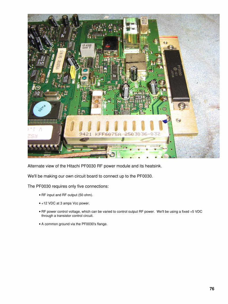
Alternate view of the Hitachi PF0030 RF power module and its heatsink.
We'll be making our own circuit board to connect up to the PF0030.
The PF0030 requires only five connections:
RF input and RF output (50 ohm).•
+12 VDC at 3 amps Vcc power.•
RF power control voltage, which can be varied to control output RF power. We'll be using a fixed +5 VDCthrough a transistor control circuit.
•
A common ground via the PF0030's flange.•
76

Making a new faceplate for the front of the amplifier's case.
It's a piece of 2−inch wide aluminum stock with a few 1/2−inch diameter holes drilled in it for theTNC RF input/output connectors and DC power banana jacks.
A new circuit board was also made for the PF0030 RF power module. This will hold the coaxialcable on the RF input/output, the power control transistor, and the voltage conditioning components.
77

Cleaning up the PF0030's heatsink and making the PC board.
I removed all the old thermal compound and sandblasted the heatsink to help clean it up a bit.
The PC board is double−sided and should have a large ground plane which is common to theheatsink.
78
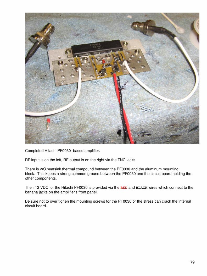
Completed Hitachi PF0030−based amplifier.
RF input is on the left, RF output is on the right via the TNC jacks.
There is NO heatsink thermal compound between the PF0030 and the aluminum mountingblock. This keeps a strong common ground between the PF0030 and the circuit board holding theother components.
The +12 VDC for the Hitachi PF0030 is provided via the RED and BLACK wires which connect to thebanana jacks on the amplifier's front panel.
Be sure not to over tighen the mounting screws for the PF0030 or the stress can crack the internalcircuit board.
79

Amplifier internal view.
The PF0030 is mounted to the aluminum base without using any heatsink compound under itsflange.
Then the aluminum base holding the PF0030 is mounted inside the case using a very thin amountof heatsink compound.
80

Finished 5 watt, 900 MHz amplifier.
RF input of around 1 mW (0 dBm) is via the TNC connector on the left.
RF output of around 2 watts (+33 dBm) is via the TNC connector on the right.
The banana jacks are for the +12 VDC power. RED is positive and BLACK is negative. Currentdraw is under 3 amps.
The optional 1,000 pF feed−thru capacitor is used for the "ground for transmit" line.
81

82