Embed Size (px)
Citation preview

Monolithic Microwave Integrated Circuits (MMIC)
Broadband Power Amplifiers
by John E. Penn
ARL-TR-6278 December 2012
Approved for public release; distribution unlimited.

NOTICES
Disclaimers
The findings in this report are not to be construed as an official Department of the Army position
unless so designated by other authorized documents.
Citation of manufacturer’s or trade names does not constitute an official endorsement or
approval of the use thereof.
Destroy this report when it is no longer needed. Do not return it to the originator.
Army Research Laboratory Adelphi, MD 20783-1197
ARL-TR-6278 December 2012
Monolithic Microwave Integrated Circuits (MMIC)
Broadband Power Amplifiers
John E. Penn
Sensors and Electron Devices Directorate, ARL
Approved for public release; distribution unlimited.

ii
REPORT DOCUMENTATION PAGE Form Approved
OMB No. 0704-0188 Public reporting burden for this collection of information is estimated to average 1 hour per response, including the time for reviewing instructions, searching existing data sources, gathering and maintaining the
data needed, and completing and reviewing the collection information. Send comments regarding this burden estimate or any other aspect of this collection of information, including suggestions for reducing the
burden, to Department of Defense, Washington Headquarters Services, Directorate for Information Operations and Reports (0704-0188), 1215 Jefferson Davis Highway, Suite 1204, Arlington, VA 22202-4302.
Respondents should be aware that notwithstanding any other provision of law, no person shall be subject to any penalty for failing to comply with a collection of information if it does not display a currently
valid OMB control number.
PLEASE DO NOT RETURN YOUR FORM TO THE ABOVE ADDRESS.
1. REPORT DATE (DD-MM-YYYY)
December 2012
2. REPORT TYPE
Final
3. DATES COVERED (From - To)
4. TITLE AND SUBTITLE
Monolithic Microwave Integrated Circuits (MMIC) Broadband Power
Amplifiers
5a. CONTRACT NUMBER
5b. GRANT NUMBER
5c. PROGRAM ELEMENT NUMBER
6. AUTHOR(S)
John E. Penn
5d. PROJECT NUMBER
5e. TASK NUMBER
5f. WORK UNIT NUMBER
7. PERFORMING ORGANIZATION NAME(S) AND ADDRESS(ES)
U.S. Army Research Laboratory
ATTN: RDRL-SER-E
2800 Powder Mill Road
Adelphi, MD 20783-1197
8. PERFORMING ORGANIZATION REPORT NUMBER
ARL-TR-6278
9. SPONSORING/MONITORING AGENCY NAME(S) AND ADDRESS(ES)
10. SPONSOR/MONITOR'S ACRONYM(S)
11. SPONSOR/MONITOR'S REPORT NUMBER(S)
12. DISTRIBUTION/AVAILABILITY STATEMENT
Approved for public release; distribution unlimited.
13. SUPPLEMENTARY NOTES
14. ABSTRACT
A broadband power amplifier design approach was used to design several monolithic microwave integrated circuits (MMICs)
using a 0.13-µm gallium arsenide (GaAs) pseudomorphic high electron mobility transistor (PHEMT) process from TriQuint
Semiconductor. The design and fabrication of these circuits were performed as part of the fall 2011 Johns Hopkins University
(JHU) MMIC Design Course, taught by the author. The design approach is taught by Dale Dawson in the JHU Power MMIC
Design Course. This approach is useful for designing relatively broadband amplifiers that are limited only be the active
transistor’s “Q”.
15. SUBJECT TERMS
MMIC, power amplifier, broadband
16. SECURITY CLASSIFICATION OF: 17. LIMITATION
OF ABSTRACT
UU
18. NUMBER OF
PAGES
34
19a. NAME OF RESPONSIBLE PERSON
John E. Penn
a. REPORT
Unclassified
b. ABSTRACT
Unclassified
c. THIS PAGE
Unclassified
19b. TELEPHONE NUMBER (Include area code)
(301) 394-0423
Standard Form 298 (Rev. 8/98)
Prescribed by ANSI Std. Z39.18
iii
Contents
List of Figures iv
List of Tables v
Acknowledgments vi
1. Introduction 1
2. Broadband Power Amplifier Device Limitations (“Q”) 1
3. Nonlinear “Software” Load-pull Simulations 3
4. Double-Q Broadband Output Match 5
5. Broadband Input Match 7
6. A 2‒6 GHz Broadband Power Amplifier 10
7. Measured Results and Sonnet EM 13
8. The Challenge of Higher Frequency: 28-GHz Broadband Power Amplifier 18
9. Conclusion 24
Distribution List 26

iv
List of Figures
Figure 1. DC I-V characteristics of 6x50 µm PHEMT (TQP13 process). ......................................2
Figure 2. Small signal S22 (output impedance) of 6x50 µm PHEMT. ..........................................2
Figure 3. An 8-GHz load pull-simulation of output power (Pcomp-6x50 µm PHEMT). .............4
Figure 4. An 8-GHz load-pull simulation of PAE (6x50 µm PHEMT). ........................................4
Figure 5. Ideal double-Q matched output. ......................................................................................5
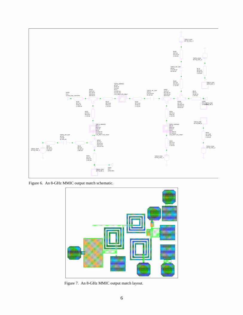
Figure 6. An 8-GHz MMIC output match schematic. ....................................................................6
Figure 7. An 8-GHz MMIC output match layout. ..........................................................................6
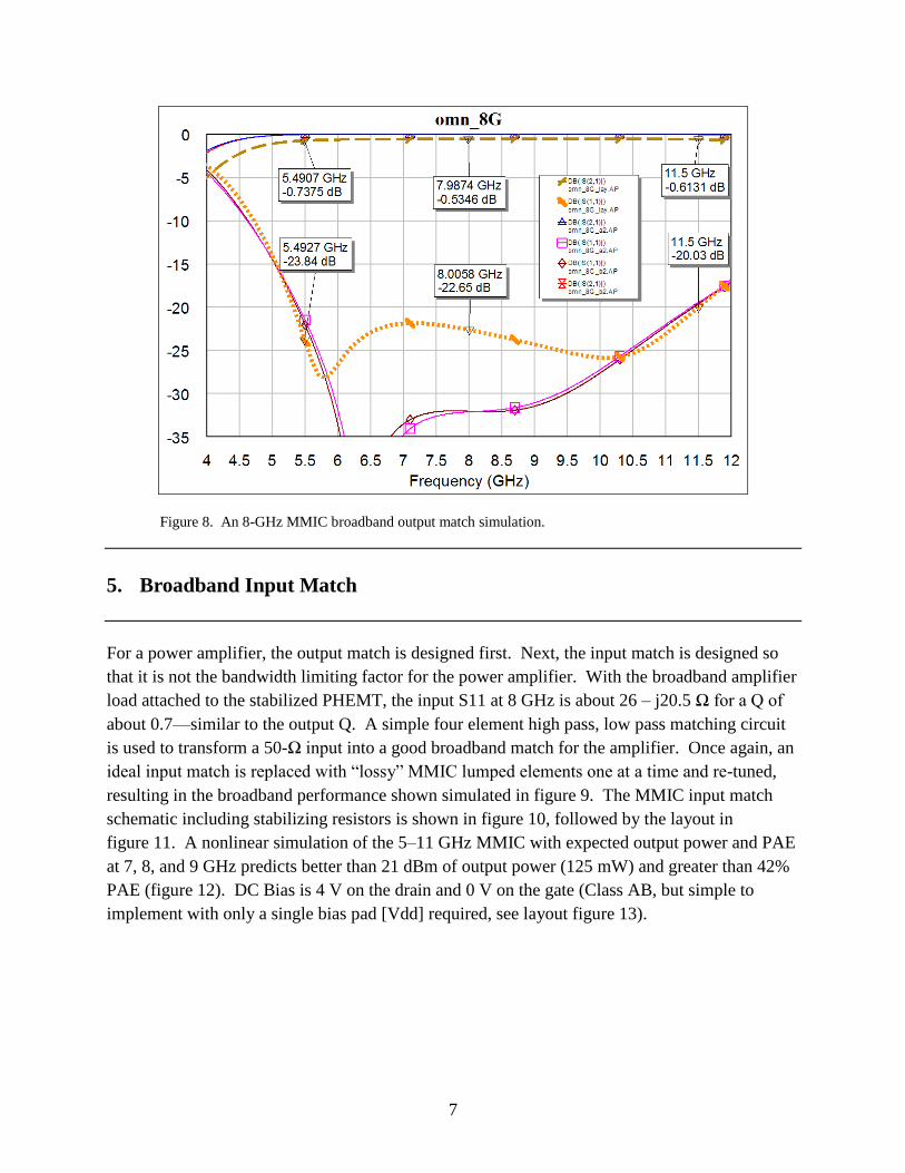
Figure 8. An 8-GHz MMIC broadband output match simulation. .................................................7
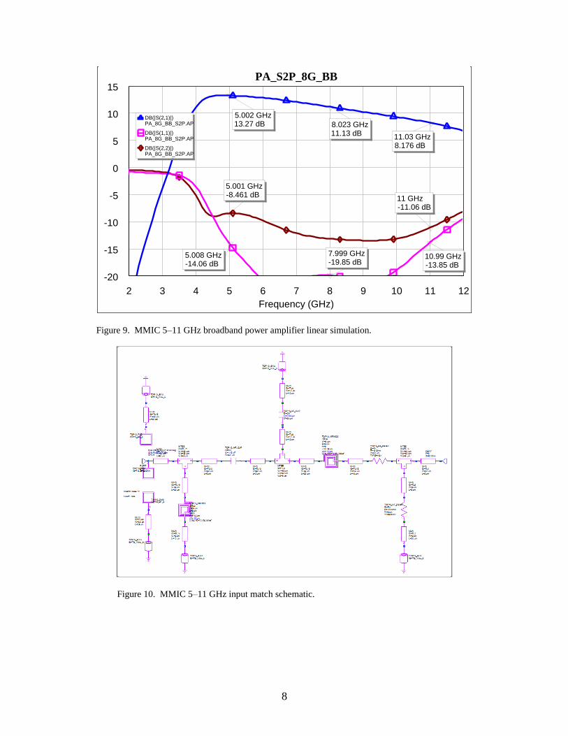
Figure 9. MMIC 5–11 GHz broadband power amplifier linear simulation. ...................................8
Figure 10. MMIC 5–11 GHz input match schematic. ....................................................................8
Figure 11. MMIC 5–11 GHz input match layout. ..........................................................................9
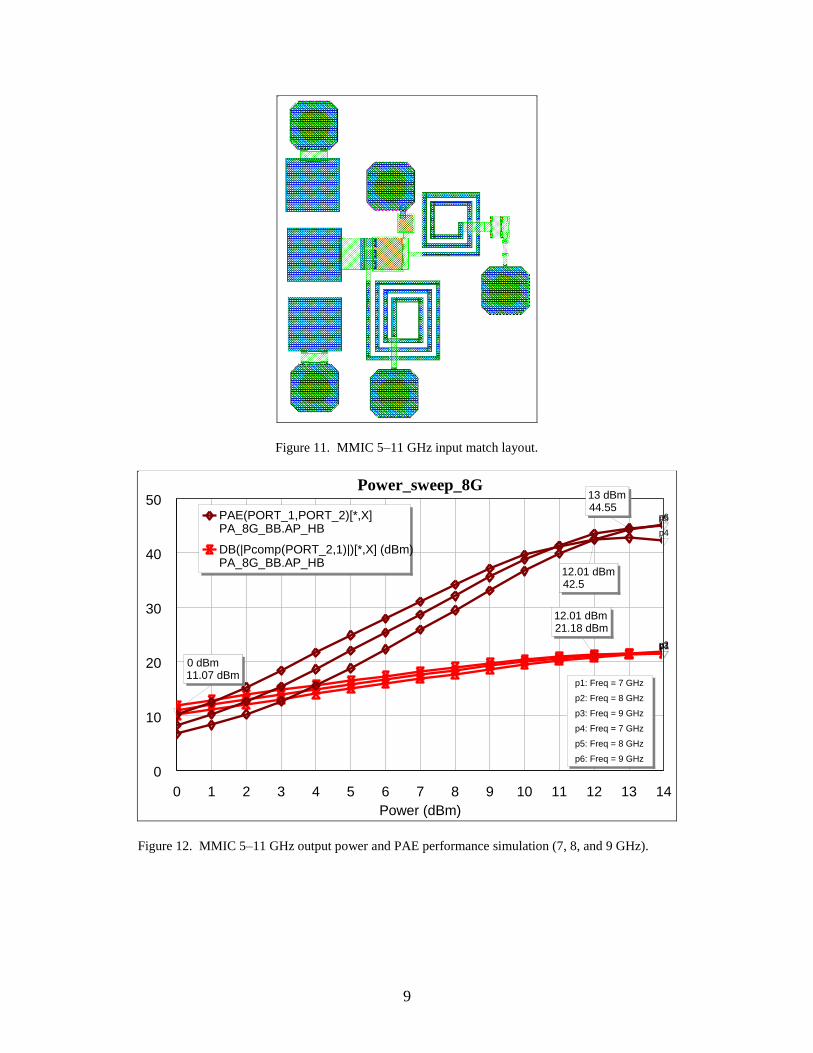
Figure 12. MMIC 5–11 GHz output power and PAE performance simulation (7, 8, and 9 GHz). .......................................................................................................................................9
Figure 13. Layout plot of the 5–11 GHz power amplifier (~1.1x0.55 mm). ................................10
Figure 14. Layout plot of the 2–6 GHz power amplifier (~1.2x0.6 mm). ....................................11
Figure 15. A 4-GHz load-pull simulation of output power (Pcomp-6x50 µm PHEMT). ...........11
Figure 16. A 4-GHz load-pull simulation of PAE (6x50 µm PHEMT). ......................................12
Figure 17. MMIC 2–6 GHz broadband power amplifier linear simulation. .................................12
Figure 18. MMIC 2–6 GHz output power and PAE performance simulation (3, 4, and 5 GHz). .....................................................................................................................................13
Figure 19. S-parameters of the 2–6 GHz broadband power amplifier (measured-solid, MWO-dot/dash, and sonnet--dotted). .....................................................................................14
Figure 20. S-parameters of the 5–11 GHz broadband power amplifier (measured-solid, MWO-dot/dash, and Sonnet--dotted).......................................................................................14
Figure 21. Power performance of the 2–6 GHz amplifier at 4 GHz (4 V). ..................................15
Figure 22. Power performance of the 5–11 GHz amplifier at 7 GHz (4 V). ................................16
Figure 23. Power performance of the 2–6 GHz amplifier at 4 GHz (3.5, 4, and 4.5 V). .............17
Figure 24. Power performance of the 5–11 GHz amplifier at 8 GHz (3.5, 4, and 4.5 V). ...........17
Figure 25. Schematic of the stabilized 6x50 µm PHEMT for a 28-GHz amplifier load-pull simulation. ................................................................................................................................19
Figure 26. A 28-GHz load-pull simulation of output power (Pcomp-6x50 µm PHEMT). ..........20
Figure 27. A 28-GHz load-pull simulation of PAE (6x50 µm PHEMT). ....................................20

v
Figure 28. A 28-GHz MMIC output match schematic. ................................................................21
Figure 29. A 28-GHz MMIC broadband output match simulation. .............................................21
Figure 30. 28 GHz broadband power amplifier—measured vs. simulation (MWO and Sonnet). ....................................................................................................................................22
Figure 31. Layout plot of the 28-GHz broadband power amplifier (~0.9x0.5 mm). ....................23
Figure 32. MMIC 28-GHz output power and PAE performance simulation (28, 30, and 32 GHz). ...................................................................................................................................23
Figure 33. Power performance of the 28-GHz amplifier at 25.3 GHz (4 V). ................................24
List of Tables
Table 1. Power performance at 4 GHz (midband) for the 2–6 GHz broadband amplifier. ..........15
Table 2. Power performance at 7 GHz (~midband) for the 5-11 GHz broadband amplifier. .......16

vi
Acknowledgments
I would like to acknowledge the support of the U.S. Army research Laboratory (ARL) in
supporting my part-time passion of teaching the Johns Hopkins University (JHU) Monolithic
Microwave Integrated Circuits (MMIC) Design Course, as well as TriQuint Semiconductor for
fabricating designs for JHU students since 1989. Software support for these JHU designs is
provided by Applied Wave Research (AWR), Agilent, Inc., and Sonnet Software.

1
1. Introduction
A broadband power amplifier design approach was used to design several monolithic microwave
integrated circuits (MMICs) using a 0.13-µm gallium arsenide (GaAs) pseudomorphic high
electron mobility transistor (PHEMT) process from TriQuint Semiconductor. The design and
fabrication of these circuits were performed as part of the fall 2011 Johns Hopkins University
(JHU) MMIC Design Course, taught by the author. The design approach is taught by Dale
Dawson in the JHU Power MMIC Design Course, and is useful for designing relatively
broadband amplifiers that are only limited by the initial “Q” of the active transistor. This
fundamental limitation to the design bandwidth will be a function of the electrical characteristics
of the starting device. This same double Q matching technique was used to successfully design
two high power broadband MMIC amplifiers at 3–5 and 4–6 GHz using TriQuint’s 0.25-µm
gallium nitride (GaN) process (see ARL-TR-59871 and ARL-TR-60902).
2. Broadband Power Amplifier Device Limitations (“Q”)
The design approach starts with the limiting characteristics of the active device for the power
amplifier. A single standard-sized pseudomorphic high electron mobility transistor (PHEMT)
(6x50 µm) is used for a broadband Class A (or mildly AB) power amplifier centered around
8 GHz, and later 4 GHz for a second design. The simple “Cripps” approach, named after Steve
Cripps, models the ideal “Class A” output (drain) power match of the PHEMT as a parallel
resistance (Rcripps) and parallel capacitance (CDS). To maximize the output voltage and current
swings, the Rcripps value is determined from a DC current-voltage (I-V) load line (figure 1).
The nonlinear shunt output capacitance is assumed to be close to the linear output capacitance,
which is determined by fitting the output match to a parallel resistance (RDS) and a parallel
capacitance (CDS) (figure 2). RDS is not actually needed and will be replaced by Rcripps. The
output matching circuit is then designed based on the parallel combination of CDS and Rcripps
obtained from these first two steps. Rcripps is approximately 50 Ω (6.5 V swing/130 mA) and
the output capacitance is approximately 400 fF at 8 GHz. It should be noted that the PHEMT
was already stabilized with a series gate resistance of 18 Ω plus a shunt resistance of 120 Ω.
There may be a subtle difference between the match of the stabilized PHEMT versus an
unstabilized PHEMT, but then the Cripps method is an approximation, and I prefer to stabilize
1Penn, John E. Broadband, Efficient, Lineaer C-Band Power Amplifiers Designed in a 0.25-µm Gallium Nitride (GaN)
Foundry Process from TriQuint Semiconductor; ARL-TR-5987; U.S. Army Research Laboratory: Adelphi, MD, 2012.
2Penn, John E. Testing of Two Broadband, Efficient, Lineaer C-Band Power Amplifiers Designed in a 0.25-µm Gallium
Nitride (GaN) Foundry Process from TriQuint Semiconductor; ARL-TR-6090; U.S. Army Research Laboratory: Adelphi, MD,
2012.

2
the device at the start. If the active device was unilateral (S12=0), then the output match would
not change due to stabilizing resistors on the input (gate). The ratio of the complex impedance to
the real impedance of the output match is the “Q” or limiting factor to bandwidth.
Figure 1. DC I-V characteristics of 6x50 µm PHEMT (TQP13 process).
Figure 2. Small signal S22 (output impedance) of 6x50 µm PHEMT.
7.25V, 0mA
3
3. Nonlinear “Software” Load-pull Simulations
The beauty of the Cripps approach is that the design can start with just DC I-V curves and S-
parameters, which are usually easy to obtain or measure. If a good nonlinear model exists, the
Cripps approach is still useful as a starting point for the design, and then nonlinear simulations
can be performed to iterate and optimize the amplifier design. Many of the computer-aided
design (CAD) tools such as Microwave Office (MWO) have a software load-pull simulation
capability. These load-pull simulations emulate actual load-pull measurements, which require
costly test equipment, accurate measurements, and time to perform the measurements over the
desired frequencies, power levels, and DC bias conditions. One can quickly perform simulations
similar to a load-pull system at different DC biases, frequencies, and power levels, with the
limitation set by the accuracy of the nonlinear model provided to the designer.
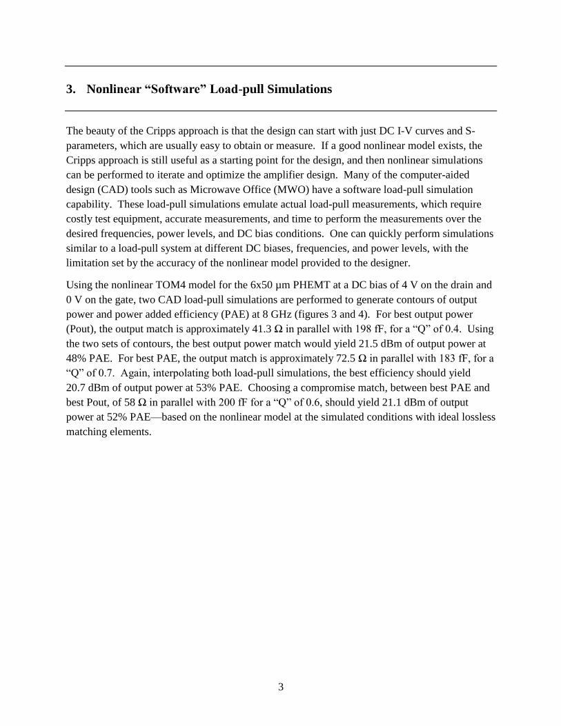
Using the nonlinear TOM4 model for the 6x50 µm PHEMT at a DC bias of 4 V on the drain and
0 V on the gate, two CAD load-pull simulations are performed to generate contours of output
power and power added efficiency (PAE) at 8 GHz (figures 3 and 4). For best output power
(Pout), the output match is approximately 41.3 Ω in parallel with 198 fF, for a “Q” of 0.4. Using
the two sets of contours, the best output power match would yield 21.5 dBm of output power at
48% PAE. For best PAE, the output match is approximately 72.5 Ω in parallel with 183 fF, for a
“Q” of 0.7. Again, interpolating both load-pull simulations, the best efficiency should yield
20.7 dBm of output power at 53% PAE. Choosing a compromise match, between best PAE and
best Pout, of 58 Ω in parallel with 200 fF for a “Q” of 0.6, should yield 21.1 dBm of output
power at 52% PAE—based on the nonlinear model at the simulated conditions with ideal lossless
matching elements.
4
Figure 3. An 8-GHz load pull-simulation of output power
(Pcomp-6x50 µm PHEMT).
Figure 4. An 8-GHz load-pull simulation of PAE (6x50 µm PHEMT).
5
4. Double-Q Broadband Output Match
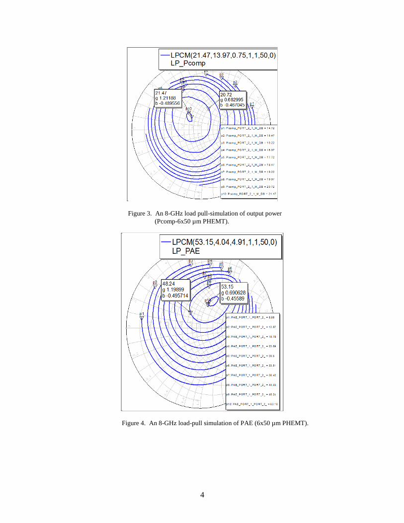
The lower the “Q” of the device, the broader the bandwidth can be—assuming ideal matching
elements. The details of the approach taught in the Johns Hopkins University (JHU) Power
Monolithic Microwave Integrated Circuits (MMIC) Design Course is summarized as a
combination of a filter techniques and impedance transforms. After creating the initial ideal
element output match, each ideal element is transformed into an equivalent MMIC “lossy”
lumped element. This is where the science blends into “art” as each ideal element is replaced
with a non-ideal element and the design is “re-tuned.” Results will vary with each design and
will likely increase in difficult with higher “Q”s and at higher frequency.
Figure 5 shows an initial ideal match, which consists of a parallel inductor (Lpar) to resonate out
CDS at 8 GHz, then a series inductor/capacitor pair at twice the “Q” value, followed by a parallel
output of the Rcripps, CDS, and Lpar. After a couple of transforms and replacing ideal elements
with “lossy” MMIC lumped elements, the final matching circuit to 50 Ω is shown in figure 6,
followed by the actual layout in figure 7. While the ideal match to the parallel RC model has
little mismatch loss, the actual MMIC match has 0.5 to 0.75 dB of insertion loss over a large
5-GHz bandwidth around 8 GHz, as shown in figure 8 (note markers).
Figure 5. Ideal double-Q matched output.
6
Figure 6. An 8-GHz MMIC output match schematic.
Figure 7. An 8-GHz MMIC output match layout.
1
2
3
MTEEID=TL5W1=8 umW2=8 umW3=20 um
1 2
3
MTEEID=TL3W1=60 umW2=60 umW3=8 um
MLINID=TL89W=50 umL=25 um
MLINID=TL15W=50 umL=25 um
MLINID=TL11W=20 umL=20 um
MLINID=TL9W=8 umL=10 um
MLINID=TL8W=10 umL=10 um
MLINID=TL7W=8 umL=20 um
MLINID=TL6W=10 umL=10 um
MLINID=TL4W=8 umL=200 um
MLINID=TL2W=20 umL=85 um
MLINID=TL1W=60 umL=50 um
TQP13_MRIND2ID=L8W=8 umS=8 umN=13L1=140 umL2=135 umLVS_IND="LVS_Value"
TQP13_HF_CAPID=C6C=0.192 pFW=30 um
TQP13_SVIAID=TQ_VIAL_4
12
3
MTEEID=TL17W1=60 umW2=40 umW3=8 um
MLINID=TL16W=8 umL=10 um
MLINID=TL14W=8 umL=10 um
TQP13_SVIAID=TQ_VIAL_8
TQP13_SVIAID=TQ_VIAL_5
TQP13_SVIAID=TQ_VIAL_3
TQP13_SVIAID=TQ_VIAL_2
1
TQP13_PADID=TQ_BP_8
1
TQP13_PADID=TQ_BP_3
1
TQP13_PADID=TQ_BP_2
1
TQP13_PADID=TQ_BP_1
TQP13_HF_CAPID=C5C=8 pFW=125 um
TQP13_HF_CAPID=C4C=0.312 pFW=40 um
1 2
3
MTEEID=TL10W1=8 umW2=8 umW3=8 um
PORTP=3Z=50 Ohm
PORTP=2Z=50 Ohm
PORTP=1Z=Conj_Opt_Load Ohm
MLINID=TL19W=8 umL=10 um
TQP13_MRIND2ID=L3W=8 umS=8 umN=13L1=140 umL2=125 umLVS_IND="LVS_Value"
MLINID=TL18W=8 umL=10 um
TQP13_MRIND2ID=L9W=8 umS=8 umN=13L1=120 umL2=121 umLVS_IND="LVS_Value"
7
Figure 8. An 8-GHz MMIC broadband output match simulation.
5. Broadband Input Match
For a power amplifier, the output match is designed first. Next, the input match is designed so
that it is not the bandwidth limiting factor for the power amplifier. With the broadband amplifier
load attached to the stabilized PHEMT, the input S11 at 8 GHz is about 26 ‒ j20.5 Ω for a Q of
about 0.7—similar to the output Q. A simple four element high pass, low pass matching circuit
is used to transform a 50-Ω input into a good broadband match for the amplifier. Once again, an
ideal input match is replaced with “lossy” MMIC lumped elements one at a time and re-tuned,
resulting in the broadband performance shown simulated in figure 9. The MMIC input match
schematic including stabilizing resistors is shown in figure 10, followed by the layout in
figure 11. A nonlinear simulation of the 5–11 GHz MMIC with expected output power and PAE
at 7, 8, and 9 GHz predicts better than 21 dBm of output power (125 mW) and greater than 42%
PAE (figure 12). DC Bias is 4 V on the drain and 0 V on the gate (Class AB, but simple to
implement with only a single bias pad [Vdd] required, see layout figure 13).
8
Figure 9. MMIC 5–11 GHz broadband power amplifier linear simulation.
Figure 10. MMIC 5–11 GHz input match schematic.
2 3 4 5 6 7 8 9 10 11 12
Frequency (GHz)
PA_S2P_8G_BB
-20
-15
-10
-5
0
5
10
15
7.999 GHz-19.85 dB
10.99 GHz-13.85 dB
5.008 GHz-14.06 dB
11 GHz-11.06 dB
5.001 GHz-8.461 dB
11.03 GHz8.176 dB
5.002 GHz13.27 dB 8.023 GHz
11.13 dB
DB(|S(2,1)|)PA_8G_BB_S2P.AP
DB(|S(1,1)|)PA_8G_BB_S2P.AP
DB(|S(2,2)|)PA_8G_BB_S2P.AP
9
Figure 11. MMIC 5–11 GHz input match layout.
Figure 12. MMIC 5–11 GHz output power and PAE performance simulation (7, 8, and 9 GHz).
0 1 2 3 4 5 6 7 8 9 10 11 12 13 14
Power (dBm)
Power_sweep_8G
0
10
20
30
40
50p6p5
p4
p3p2p1
0 dBm11.07 dBm
13 dBm44.55
12.01 dBm42.5
12.01 dBm21.18 dBm
PAE(PORT_1,PORT_2)[*,X]PA_8G_BB.AP_HB
DB(|Pcomp(PORT_2,1)|)[*,X] (dBm)PA_8G_BB.AP_HB
p1: Freq = 7 GHz
p2: Freq = 8 GHz
p3: Freq = 9 GHz
p4: Freq = 7 GHz
p5: Freq = 8 GHz
p6: Freq = 9 GHz

10
Figure 13. Layout plot of the 5–11 GHz power amplifier (~1.1x0.55 mm).
6. A 2‒6 GHz Broadband Power Amplifier
The same design approach was used to center a design at 4 GHz. Topology and design steps are
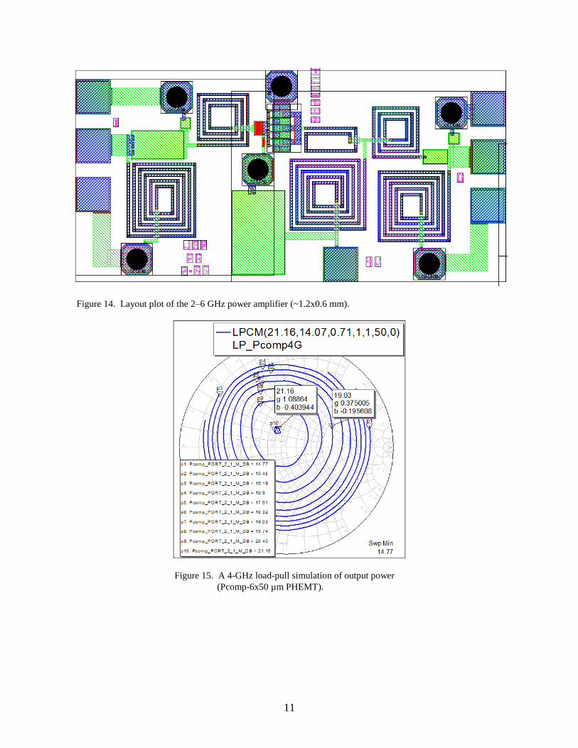
identical, resulting in a slightly larger layout at the lower frequency, as shown in figure 14.
Again, a compromise was struck between the best output power and best efficiency using the
nonlinear load-pull contours (figures 15 and 16). Best output match is approximately 45 Ω in
parallel with 320 fF, for a “Q” of 0.4. Using the two sets of contours, the best output power
match would yield 21.1 dBm of output power at 52% PAE. For best power added efficiency, the
output match is approximately 132.5 Ω in parallel with 194 fF, for a “Q” of 0.65. Again,
interpolating both load-pull simulations, the best efficiency should yield 19.3 dBm of output
power at 59% PAE. Choosing a compromise match, between best PAE and best Pout, of 58 Ω in
parallel with 290 fF for a “Q” of 0.45, should yield 20.8 dBm of output power at 54% PAE—
based on the nonlinear model at the simulated conditions with ideal lossless matching elements.
11
Figure 14. Layout plot of the 2–6 GHz power amplifier (~1.2x0.6 mm).
Figure 15. A 4-GHz load-pull simulation of output power
(Pcomp-6x50 µm PHEMT).
12
Figure 16. A 4-GHz load-pull simulation of PAE (6x50 µm PHEMT).
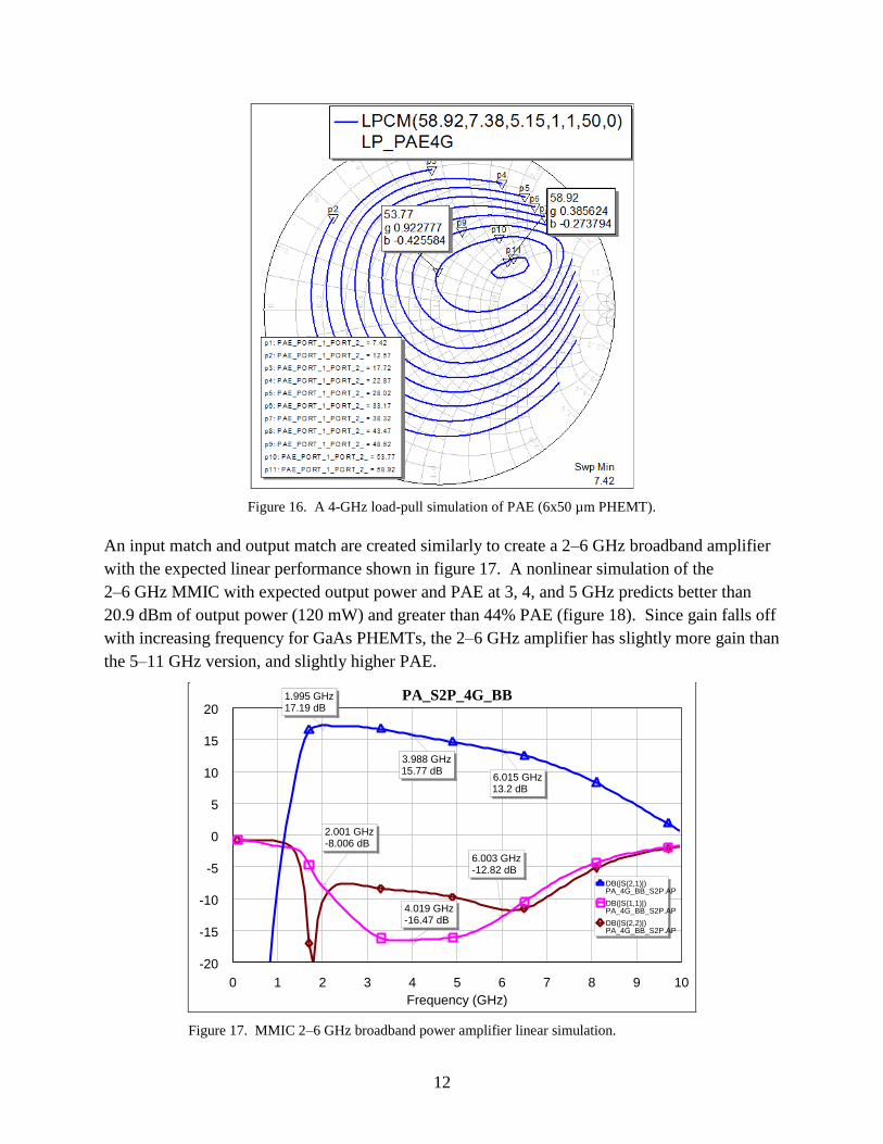
An input match and output match are created similarly to create a 2–6 GHz broadband amplifier
with the expected linear performance shown in figure 17. A nonlinear simulation of the
2–6 GHz MMIC with expected output power and PAE at 3, 4, and 5 GHz predicts better than
20.9 dBm of output power (120 mW) and greater than 44% PAE (figure 18). Since gain falls off
with increasing frequency for GaAs PHEMTs, the 2–6 GHz amplifier has slightly more gain than
the 5–11 GHz version, and slightly higher PAE.
Figure 17. MMIC 2–6 GHz broadband power amplifier linear simulation.
0 1 2 3 4 5 6 7 8 9 10
Frequency (GHz)
PA_S2P_4G_BB
-20
-15
-10
-5
0
5
10
15
20
4.019 GHz-16.47 dB
3.988 GHz15.77 dB
6.003 GHz-12.82 dB
2.001 GHz-8.006 dB
6.015 GHz13.2 dB
1.995 GHz17.19 dB
DB(|S(2,1)|)PA_4G_BB_S2P.AP
DB(|S(1,1)|)PA_4G_BB_S2P.AP
DB(|S(2,2)|)PA_4G_BB_S2P.AP

13
Figure 18. MMIC 2–6 GHz output power and PAE performance simulation (3, 4, and 5 GHz).
7. Measured Results and Sonnet EM
Sonnet electromagnetic (EM) simulations were performed based on the actual physical layouts of
both amplifier designs to look for parasitic coupling that might be un-simulated in a linear
simulator, but the differences were slight. The S-parameter measurements agree very well with
the original MWO simulations. Figures 19 and 20 show the measured versus MWO versus
Sonnet EM simulations, showing good agreement. Power performance was lower than
predicted. Measurements were taken at the designed for bias of 4 V yielding slightly less output
power and lower PAE, though the results compared similarly across the broadband. Efficiencies
were slightly better with the higher gain 2–6 GHz broadband power amplifier. Additionally,
performance was measured with a supply voltage of 3.5, 4, and 4.5 V, showing more output
power with a higher DC supply but better PAE at 3.5 V—as might be expected. This was true of
both amplifiers; the only real difference was the operating frequency, either 2–6 or 5–11 GHz.
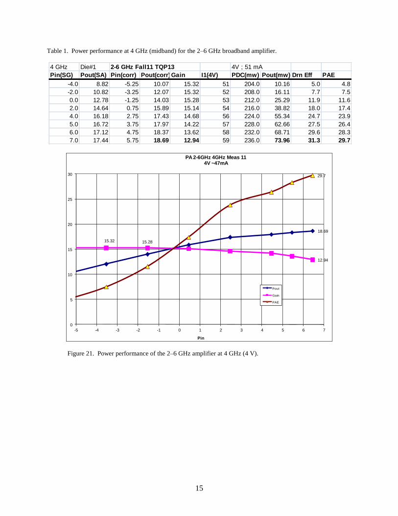
Table 1 and figure 21 summarize the performance of the 2–6 GHz amplifier at midband (4 GHz).
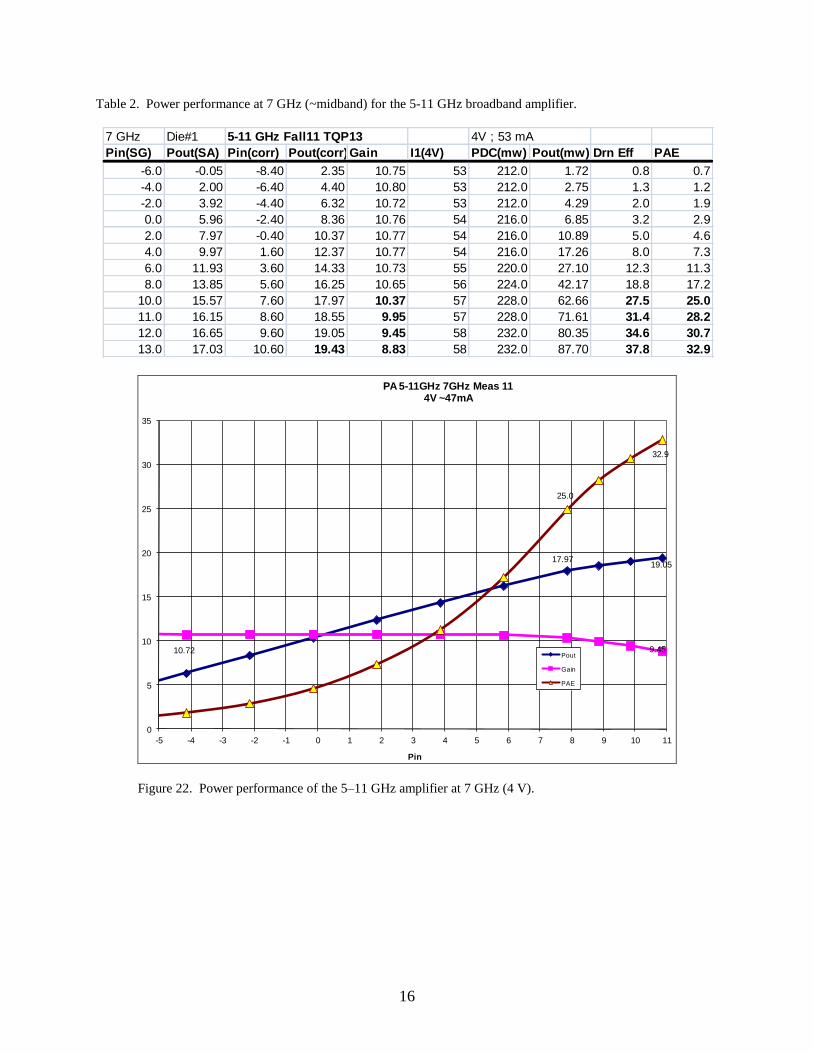
Likewise, table 2 and figure 22 summarize the performance of the 5–11 GHz amplifier at 7 GHz.
Plots of performance at 3.5, 4, and 4.5 V for the 2–6 GHz amplifier at 4 GHz are shown in
figure 23, with more output power at the higher voltage but better efficiency at the lower voltage.
Likewise, plots of performance at 3.5, 4, and 4.5 V for the 5–11 GHz amplifier at 8 GHz are
shown in figure 24, with more output power at the higher voltage but better efficiency at the
lower voltage. Both amplifiers worked well with the broadband matching techniques and acted
similarly in performance over their band of operation.
0 1 2 3 4 5 6 7 8 9 10
Power (dBm)
Power_sweep_4G
10
15
20
25
30
35
40
45
50
55
p6
p5
p4
p3p2p1
0 dBm15.33 dBm
9.025 dBm20.94 dBm
9.012 dBm43.85
9.002 dBm50.14PAE(PORT_1,PORT_2)[*,X]
PA_4G_BB.AP_HB
DB(|Pcomp(PORT_2,1)|)[*,X] (dBm)PA_4G_BB.AP_HB
p1: Freq = 3 GHz
p2: Freq = 4 GHz
p3: Freq = 5 GHz
p4: Freq = 3 GHz
p5: Freq = 4 GHz
p6: Freq = 5 GHz

14
Figure 19. S-parameters of the 2–6 GHz broadband power amplifier (measured-solid, MWO-dot/dash,
and sonnet--dotted).
Figure 20. S-parameters of the 5–11 GHz broadband power amplifier (measured-solid,
MWO-dot/dash, and Sonnet--dotted).
15
Table 1. Power performance at 4 GHz (midband) for the 2–6 GHz broadband amplifier.
Figure 21. Power performance of the 2–6 GHz amplifier at 4 GHz (4 V).
4 GHz Die#1 2-6 GHz Fall11 TQP13 4V ; 51 mA
Pin(SG) Pout(SA) Pin(corr) Pout(corr)Gain I1(4V) PDC(mw) Pout(mw) Drn Eff PAE
-4.0 8.82 -5.25 10.07 15.32 51 204.0 10.16 5.0 4.8
-2.0 10.82 -3.25 12.07 15.32 52 208.0 16.11 7.7 7.5
0.0 12.78 -1.25 14.03 15.28 53 212.0 25.29 11.9 11.6
2.0 14.64 0.75 15.89 15.14 54 216.0 38.82 18.0 17.4
4.0 16.18 2.75 17.43 14.68 56 224.0 55.34 24.7 23.9
5.0 16.72 3.75 17.97 14.22 57 228.0 62.66 27.5 26.4
6.0 17.12 4.75 18.37 13.62 58 232.0 68.71 29.6 28.3
7.0 17.44 5.75 18.69 12.94 59 236.0 73.96 31.3 29.7
18.69
15.32 15.28
12.94
29.7
0
5
10
15
20
25
30
-5 -4 -3 -2 -1 0 1 2 3 4 5 6 7
Pin
PA 2-6GHz 4GHz Meas 114V ~47mA
Pout
Gain
PAE
16
Table 2. Power performance at 7 GHz (~midband) for the 5-11 GHz broadband amplifier.
Figure 22. Power performance of the 5–11 GHz amplifier at 7 GHz (4 V).
7 GHz Die#1 5-11 GHz Fall11 TQP13 4V ; 53 mA
Pin(SG) Pout(SA) Pin(corr) Pout(corr)Gain I1(4V) PDC(mw) Pout(mw) Drn Eff PAE
-6.0 -0.05 -8.40 2.35 10.75 53 212.0 1.72 0.8 0.7
-4.0 2.00 -6.40 4.40 10.80 53 212.0 2.75 1.3 1.2
-2.0 3.92 -4.40 6.32 10.72 53 212.0 4.29 2.0 1.9
0.0 5.96 -2.40 8.36 10.76 54 216.0 6.85 3.2 2.9
2.0 7.97 -0.40 10.37 10.77 54 216.0 10.89 5.0 4.6
4.0 9.97 1.60 12.37 10.77 54 216.0 17.26 8.0 7.3
6.0 11.93 3.60 14.33 10.73 55 220.0 27.10 12.3 11.3
8.0 13.85 5.60 16.25 10.65 56 224.0 42.17 18.8 17.2
10.0 15.57 7.60 17.97 10.37 57 228.0 62.66 27.5 25.0
11.0 16.15 8.60 18.55 9.95 57 228.0 71.61 31.4 28.2
12.0 16.65 9.60 19.05 9.45 58 232.0 80.35 34.6 30.7
13.0 17.03 10.60 19.43 8.83 58 232.0 87.70 37.8 32.9
17.9719.05
10.72 10.37 9.45
25.0
32.9
0
5
10
15
20
25
30
35
-5 -4 -3 -2 -1 0 1 2 3 4 5 6 7 8 9 10 11
Pin
PA 5-11GHz 7GHz Meas 114V ~47mA
Pout
Gain
PAE
17
Figure 23. Power performance of the 2–6 GHz amplifier at 4 GHz (3.5, 4, and 4.5 V).
Figure 24. Power performance of the 5–11 GHz amplifier at 8 GHz (3.5, 4, and 4.5 V).
17.99
12.34
29.6
18.77
15.32
13.12
29.0
16.87
12.14
30.9
0
5
10
15
20
25
30
35
-5 -4 -3 -2 -1 0 1 2 3 4 5 6
Pin
PA 2-6GHz 4GHz Meas 113.5, 4, 4.5V ~50mA
Pout4VGain4VPAE4VPout4_5VGain4_5VPAE4_5VPout3_5VGain3_5VPAE3_5V
18.28
10.18
7.33
27.4
19.15
7.20
32.2
17.34
7.39
33.8
0
5
10
15
20
25
30
35
0 1 2 3 4 5 6 7 8 9 10 11 12
Pin
PA 5-11GHz 8GHz Meas 113.5, 4, 4.5V ~50mA
Pout4V
Gain4V
PAE4V
Pout4_5V
Gain4_5V
PAE4_5V
Pout3_5V
Gain3_5V
PAE3_5V

18
8. The Challenge of Higher Frequency: 28-GHz Broadband Power
Amplifier
The same design approach was used to attempt a broadband design around 28 GHz. Several
issues conspire to make this design much harder. Gain tends to fall off with frequency with
GaAs transistors, so there will be less gain and PAE at the higher frequency. To minimize the
impact in gain when stabilizing the same 6x50 µm PHEMT device used for the previous two
amplifier designs, a parallel resistor and capacitor combination is used in series with the gate
where the resistor helps the stability at low frequency and as the frequency increase, the
capacitor increasingly bypasses the resistor so that available gain at the higher frequencies is
increased. For stability, the same 120-Ω shunt resistor is used on the gate but the series resistor
becomes 25 Ω in parallel with a 1.2-pF capacitor.
A second challenge is that the “Q” of the PHEMT increases at higher frequencies resulting in a
narrower bandwidth. Third, the higher the frequency and Q increases the harder it is to convert
ideal elements into lossy MMIC elements while maintaining good performance. Initially, the
ideal matching topology and design steps are identical to the 4- and 8-GHz designs. A load-pull
simulation based on the nonlinear model of the stabilized 6x50 µm PHEMT is performed (see
schematic in figure 25). Again, the load-pull contours are used to find a compromise between
the best output power and best efficiency (figures 26 and 27). An output load equivalent to 58 Ω
in parallel with 143 fF, for a “Q” of 1.5, should yield ~19 dBm of output power at 35% PAE,
assuming ideal lossless matching elements. The schematic of the final matching circuit to 50 Ω
is shown in figure 28. Note the much narrower bandwidth and increased mismatch loss of the
broadband “lossy” MMIC output match around 28 GHz, as shown in figure 29 (note markers).
19
Figure 25. Schematic of the stabilized 6x50 µm PHEMT for a 28-GHz amplifier load-pull simulation.
20
Figure 26. A 28-GHz load-pull simulation of output power (Pcomp-6x50 µm PHEMT).
Figure 27. A 28-GHz load-pull simulation of PAE (6x50 µm PHEMT).
21
Figure 28. A 28-GHz MMIC output match schematic.
Figure 29. A 28-GHz MMIC broadband output match simulation.
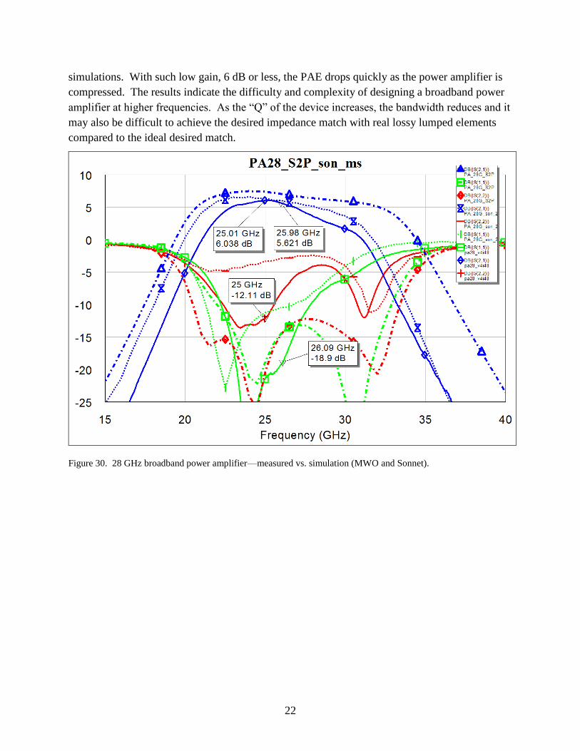
Sonnet EM simulations of the layout were performed and tended to indicate less bandwidth than
the original MWO design. The actual performance was even narrower band than either
simulation but was closer to the Sonnet simulation, as shown in figure 30. A final layout of the
broadband 28-GHz amplifier is shown in figure 31. When the performance was re-simulated
with lossy MMIC elements, the output power, gain and efficiency are much lower than the ideal
case (figure 32). Performance measurements at 25.3 GHz are much closer to these re-
1 2
3
MTEEID=TL3W1=60 umW2=60 umW3=8 um
MLINID=TL89W=50 umL=25 um
MLINID=TL15W=50 umL=25 um
MLINID=TL11W=20 umL=20 um
MLINID=TL9W=8 umL=190 um
MLINID=TL8W=10 umL=10 um
MLINID=TL7W=8 umL=20 um
MLINID=TL6W=10 umL=10 um
MLINID=TL4W=12 umL=30 um
MLINID=TL2W=20 umL=10 um
MLINID=TL1W=60 umL=50 um
TQP13_HF_CAPID=C6C=0.156 pFW=20 um
TQP13_SVIAID=TQ_VIAL_4
12
3
MTEEID=TL17W1=60 umW2=12 umW3=8 um
MLINID=TL16W=8 umL=145 um
TQP13_SVIAID=TQ_VIAL_8
TQP13_SVIAID=TQ_VIAL_5
TQP13_SVIAID=TQ_VIAL_3
TQP13_SVIAID=TQ_VIAL_2
1
TQP13_PADID=TQ_BP_8
1
TQP13_PADID=TQ_BP_3
1
TQP13_PADID=TQ_BP_2
1
TQP13_PADID=TQ_BP_1
TQP13_HF_CAPID=C5C=2.5 pFW=60 um
1 2
3
MTEEID=TL10W1=12 umW2=12 umW3=8 um
1
2
3
MTEEID=TL5W1=8 umW2=8 umW3=20 um
PORTP=3Z=50 Ohm
PORTP=2Z=50 Ohm
PORTP=1Z=Conj_Opt_Load Ohm
TQP13_MRIND2ID=L3W=12 umS=12 umN=9L1=100 umL2=135 umLVS_IND="LVS_Value"
TQP13_HF_CAPID=C7C=0.115 pFW=12 um
TQP13_HF_CAPID=C3C=0.1 pFW=12 um
Conj_Opt_Load=58/(1+j*_FREQ*6.28*0.143e-12*58)
Cser=0.034e-12
Lser=0.962
CDS=0.143
L1=0.226
Q~1.5
35% PAE, 19 dBm
PAE Match of 0.57 at 118 deg
22
simulations. With such low gain, 6 dB or less, the PAE drops quickly as the power amplifier is
compressed. The results indicate the difficulty and complexity of designing a broadband power
amplifier at higher frequencies. As the “Q” of the device increases, the bandwidth reduces and it
may also be difficult to achieve the desired impedance match with real lossy lumped elements
compared to the ideal desired match.
Figure 30. 28 GHz broadband power amplifier—measured vs. simulation (MWO and Sonnet).

23
Figure 31. Layout plot of the 28-GHz broadband power amplifier (~0.9x0.5 mm).
Figure 32. MMIC 28-GHz output power and PAE performance simulation (28, 30, and 32 GHz).

24
Figure 33. Power performance of the 28-GHz amplifier at 25.3 GHz (4 V).
9. Conclusion
These broadband medium power amplifier MMICs were designed using some of the techniques
taught by Dale Dawson in the JHU Power MMIC Course. These are the first designs that I have
performed, fabricated, and tested since helping Dr. Dawson teach the course in spring 2011.
These filter and matching techniques could be applied to parallel combinations of transistors to
increase power, but these simple one-transistor single-stage designs are a good start to prove out
the concepts and validate with actual measurements. It should be noted that these broadband
techniques were also used to successfully design two high power broadband MMIC amplifiers at
3–5 and 4–6 GHz using TriQuint’s 0.25-µm gallium nitride (GaN) process (see ARL-TR-59871
and ARL-TR-60902). These MMIC amplifiers illustrate the broadband design approach and the
limitations that start with the device parasitic, the quality of the nonlinear and linear models
available, and the quality of the MMIC fabrication process. They also illustrate the occasional
necessity for an EM simulator, such as Sonnet, to accurately predict the actual layout parasitics,
particularly at higher frequencies.
15.05 15.95
5.504.40
13.1 14.2
0
2
4
6
8
10
12
14
16
18
20
0 1 2 3 4 5 6 7 8 9 10 11 12
Pin
PA 28GHz Meas 1125.3 GHz 4V ~44mA
Pout
Gain
PAE

25
While the designs were part of a JHU course, the design techniques and Microwave MMICs
would be of interest to Army and Department of Defense (DoD) communications systems,
sensors, and wireless systems.
26
No. of
COPIES ORGANIZATION
1 DEFENSE TECHNICAL
(PDF INFORMATION CTR
only) DTIC OCA
8725 JOHN J KINGMAN RD
STE 0944
FORT BELVOIR VA 22060-6218
1 DIRECTOR
US ARMY RESEARCH LAB
IMAL HRA
2800 POWDER MILL RD
ADELPHI MD 20783-1197
1 DIRECTOR
US ARMY RESEARCH LAB
RDRL CIO LL
2800 POWDER MILL RD
ADELPHI MD 20783-1197
4 HCS DIRECTOR
7 PDFS US ARMY RESEARCH LAB
RDRL SER
PAUL AMIRTHARAJ (PDF)
RDRL SER E
ROMEO DEL ROSARIO (1 HC)
JAMES WILSON (PDF)
TONY IVANOV (PDF)
JOHN PENN (3 HCS)
ROBERT PROIE (PDF)
ROBERT REAMS (PDF)
PANKAJ SHAH (PDF)
ED VIVEIROS (PDF)
2800 POWDER MILL RD
ADELPHI MD 20783-1197
TOTAL: 14 (8 ELEC, 6 HCS)