Embed Size (px)
Citation preview

Module 4 : Propagation Delays in MOS Lecture 17 : Pseudo NMOS Inverter Objectives In this lecture you will learn the following
• Introduction • Different Configurations with NMOS Inverter • Worries about Pseudo NMOS Inverter • Calculation of Capacitive Load
17.1 Introduction The inverter that uses a p-device pull-up or load that has its gate permanently ground. An n-device pull-down or driver is driven with the input signal. This roughly equivalent to use of a depletion load is Nmos technology and is thus called ‘Pseudo-NMOS’. The circuit is used in a variety of CMOS logic circuits. In this, PMOS for most of the time will be linear region. So resistance is low and hence RC time constant is low. When the driver is turned on a constant DC current flows in the circuit.
Fig 17.1: CMOS Inverter Circuit
17.2 Different Configurations with NMOS Inverter
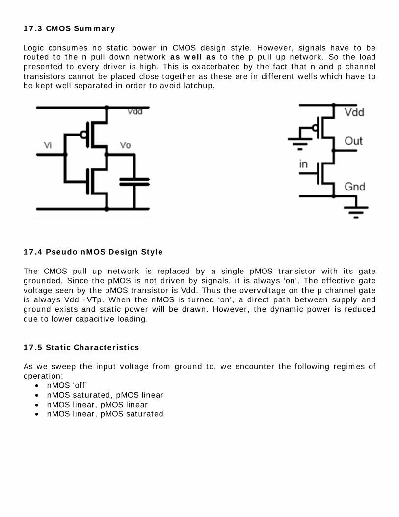
17.3 CMOS Summary Logic consumes no static power in CMOS design style. However, signals have to be routed to the n pull down network as well as to the p pull up network. So the load presented to every driver is high. This is exacerbated by the fact that n and p channel transistors cannot be placed close together as these are in different wells which have to be kept well separated in order to avoid latchup.
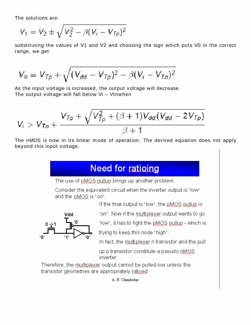
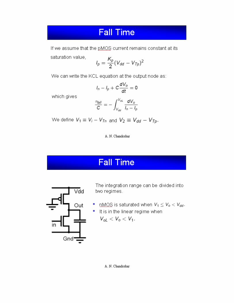
17.4 Pseudo nMOS Design Style The CMOS pull up network is replaced by a single pMOS transistor with its gate grounded. Since the pMOS is not driven by signals, it is always ‘on'. The effective gate voltage seen by the pMOS transistor is Vdd. Thus the overvoltage on the p channel gate is always Vdd -VTp. When the nMOS is turned ‘on', a direct path between supply and ground exists and static power will be drawn. However, the dynamic power is reduced due to lower capacitive loading. 17.5 Static Characteristics As we sweep the input voltage from ground to, we encounter the following regimes of operation:
• nMOS ‘off’ • nMOS saturated, pMOS linear • nMOS linear, pMOS linear • nMOS linear, pMOS saturated
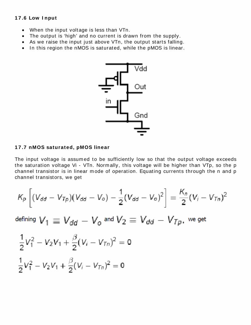
17.6 Low Input
• When the input voltage is less than VTn. • The output is ‘high’ and no current is drawn from the supply. • As we raise the input just above VTn, the output starts falling. • In this region the nMOS is saturated, while the pMOS is linear.
17.7 nMOS saturated, pMOS linear The input voltage is assumed to be sufficiently low so that the output voltage exceeds the saturation voltage Vi - VTn. Normally, this voltage will be higher than VTp, so the p channel transistor is in linear mode of operation. Equating currents through the n and p channel transistors, we get
The solutions are:
substituting the values of V1 and V2 and choosing the sign which puts V0 in the correct range, we get
As the input voltage is increased, the output voltage will decrease. The output voltage will fall below Vi – Vtnwhen
The nMOS is now in its linear mode of operation. The derived equation does not apply beyond this input voltage.
Recap In this lecture you have learnt the following
• Introduction • Different Configurations with NMOS Inverter • Worries about Pseudo NMOS Inverter • Calculation of Capacitive Load
Congratulations, you have finished Lecture 17.

![CHAPTER 12 ARRAY SUBSYSTEMS [12.4-12.9]web.cecs.pdx.edu/~chiang/ECE_426_526_Summer_2011/Manjari_S... · Pseudo-nMOS ROM ... FULL and EMPTY flags ... First In First Out [FIFO] –](https://img.dokumen.tips/doc/110x75/5ab549917f8b9a6e1c8ca011/chapter-12-array-subsystems-124-129webcecspdxeduchiangece426526summer2011manjarispseudo-nmos.jpg)