Embed Size (px)
Citation preview
Modeling and characterization of novel MOS devices
Doctoral Thesis
By
Stefan Persson
Stockholm, 2004 Sweden
Laboratory of Solid State Devices (SSD), Department of Microelectronics and Information Technology (IMIT),
Royal Institute of Technology (KTH)
Modeling and characterization of novel MOS devices
by Stefan Persson
A dissertation submitted to the Royal Institute of Technology, Stockholm, Sweden in
partial fulfillment of the requirements for the degree of Doctor of Philosophy (Ph. D.).
ISRN KTH/EKT/FR-2004/2-SE
ISSN 1650-8599
TRITA-EKT
Forskningsrapport 2004:2
This thesis is available in electronic version at:http://media.lib.kth.se
Printed by Universitetsservice US AB, Stockholm, 2004.
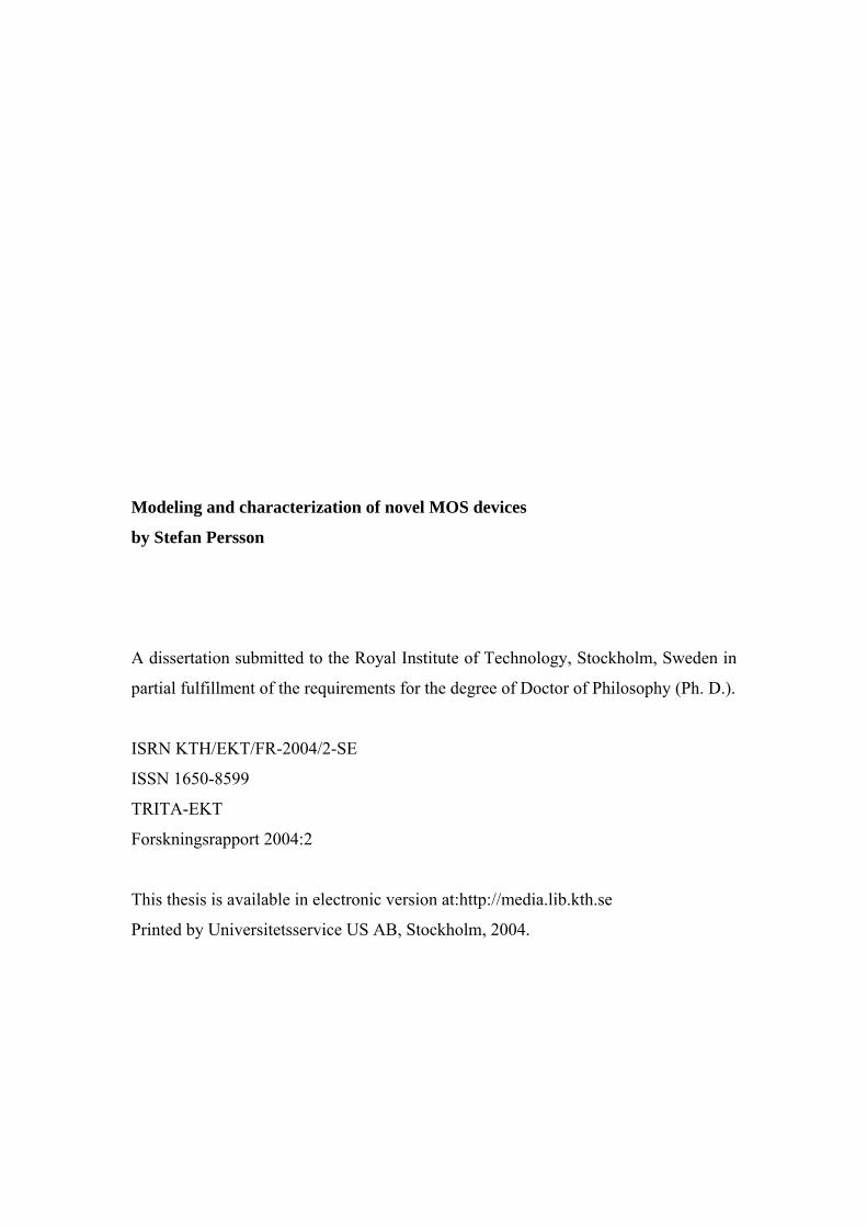
Persson, S: Modeling and characterization of novel MOS devices ISRN KTH/EKT/FR-2004/2-SE, ISSN 1650-8599, TRITA-EKT, Forskningsrapport 2004:2 Royal Institute of technology (KTH), Department of Microelectronics and Information technology (IMIT), Stockholm 2004.
Abstract
Challenges with integrating high-κ gate dielectric, retrograde Si1-xGex channel and silicided contacts in future CMOS technologies are investigated experimentally and theoretically in this thesis. pMOSFETs with either Si or strained Si1-xGex surface-channel and different high-κ gate dielectric are examined. Si1-xGex pMOSFETs with an Al2O3/HfAlOx/Al2O3 nano-laminate gate dielectric prepared by means of Atomic Layer Deposition (ALD) exhibit a great-than-30% increase in current drive and peak transconductance compared to reference Si pMOSFETs with the same gate dielectric. A poor high-κ/Si interface leading to carrier mobility degradation has often been reported in the literature, but this does not seem to be the case for our Si pMOSFETs whose effective mobility coincides with the universal hole mobility curve for Si. For the Si1-xGex pMOSFETs, however, a high density of interface states giving rise to reduced carrier mobility is observed. A method to extract the correct mobility in the presence of high-density traps is presented. Coulomb scattering from the charged traps or trapped charges at the interface is found to play a dominant role in the observed mobility degradation in the Si1-xGex pMOSFETs.
Studying contacts with metal silicides constitutes a major part of this thesis. With the conventional device fabrication, the Si1-xGex incorporated for channel applications inevitably extends to the source-drain areas. Measurement and modeling show that the presence of Ge in the source/drain areas positively affects the contact resistivity in such a way that it is decreased by an order of magnitude for the contact of TiW to p-type Si1-xGex/Si when the Ge content is increased from 0 to 30 at. %. Modeling and extraction of contact resistivity are first carried out for the traditional TiSi2-Si contact but with an emphasis on the influence of a Nb interlayer for the silicide formation. A two-dimensional numerical model is employed to account for effects due to current crowding. For more advanced contacts to ultra-shallow junctions, Ni-based metallization scheme is used. NiSi1-xGex is found to form on selectively grown p-type Si1-xGex used as low-resistivity source/drain. Since the formed NiSi1-xGex with a specific resistivity of 20 µΩcm replaces a significant fraction of the shallow junction, a three-dimensional numerical model is employed in order to take the complex interface geometry and morphology into account. The lowest contact resistivity obtained for our NiSi1-xGex/p-type Si1-xGex contacts is 5×10⁻⁸ Ωcm2, which satisfies the requirement for the 45-nm technology node in 2010.
When the Si1-xGex channel is incorporated in a MOSFET, it usually forms a retrograde channel with an undoped surface region on a moderately doped substrate. Charge sheet models are used to study the effects of a Si retrograde channel on surface potential, drain current, intrinsic charges and intrinsic capacitances. Closed-form solutions are found for an abrupt retrograde channel and results implicative for circuit designers are obtained. The model can be extended to include a Si1-xGex retrograde channel. Although the analytical model developed in this thesis is one-dimensional for long-channel transistors with the retrograde channel profile varying along the depth of the transistor, it should also be applicable for short-channel transistors provided that the short channel effects are perfectly controlled. Key Words
MOSFET, SiGe, high-κ dielectric, metal gate, mobility, charge sheet model, retrograde channel structure, intrinsic charge, intrinsic capacitance, contact resistivity.


i
Table of content
List of papers ________________________________________________________ii
Summary of Appended Papers _________________________________________ iii
Acknowledgements____________________________________________________v
List of Symbols ______________________________________________________vii
1. Introduction _____________________________________________________1
2. Operation of MOSFET ____________________________________________5
2.1 Basic MOSFET theory ________________________________________5
2.2 Scaling trend, short cannel effect, thin oxide and series resistance_____7
3. Gate Stack______________________________________________________13
3.1 Metal and semiconductor as gate material _______________________13
3.2 High-κ gate dielectrics ________________________________________13
3.3 Gate oxide-channel interface and interface traps__________________17
3.4 Effects of interface traps on mobility and mobility measurement ____21
4. Channel Structure _______________________________________________25
4.1 Charge sheet model __________________________________________25
4.2 Retrograde channel __________________________________________26
4.3 Si1-xGex channel _____________________________________________29
5. Source and Drain Resistance ______________________________________33
5.1 Source and drain series resistance ______________________________33
5.2 Methods for measurement of metal-semiconductor contact resistivity 35
5.3 Choice of metal silicides for contact formation____________________37
5.4 Modeling of CBK structure____________________________________39
6. Summary_______________________________________________________45
7. References _____________________________________________________47

ii
List of papers
Papers on which the thesis is based: I. D. Wu, A.-C. Lindgren, S. Persson, G. Sjöblom, M. von Haartman, J. Seger, P.-E. Hellström, J. Olsson, H.-O. Blom, S.-L. Zhang, M. Östling, E. Vainonen-Ahlgren, W.-M. Li, E. Tois, and M. Tuominen, “A novel strained Si0.7Ge0.3 surface-channel pMOSFET with ALD TiN/Al2O3/HfAlOx/Al2O3 gate stack,” IEEE Electron Device Lett., Vol. 24, pp. 171-173, March 2003. II. D. Wu, S. Persson, A.-C. Lindgren, G. Sjöblom, P.-E. Hellström, J. Olsson, S.-L. Zhang, M. Östling, E. Vainonen-Ahlgren, E. Tois, W.-M. Li, and M. Tuominen, “ALD metal-gate/high-κ gate stack for Si and Si0.7Ge0.3 surface-channel pMOSFETs,” In the 33th proc. ESSDREC 2003, pp. 263-266. III. S. Persson, D. Wu, P.-E. Hellberg, S.-L. Zhang, and M. Östling, “Quantifying hole mobility degradation in pMOSFETs with a strained-Si0.7Ge0.3 surface-channel under an ALD TiN/Al2O3/HfAlOx/Al2O3 gate stack,” Solid-State Electron. (in press). IV. S. Persson, P.-E. Hellberg, and S.-L. Zhang, “A charge sheet model for MOSFETs with an abrupt retrograde channel – Part I. Drain current and body charge,” Solid-State Electron., Vol. 46, pp. 2209-2216, 2002. V. S. Persson, P.-E. Hellberg, and S.-L. Zhang, “A charge sheet model for MOSFETs with an abrupt retrograde channel – Part II. Charges and intrinsic capacitances,” Solid-State Electron., Vol. 46, pp. 2217-2225, 2002. VI. J. Åberg, S. Persson, P.-E. Hellberg, S.-L. Zhang, U. Smith, F. Ericson, M. Engström, and W. Kaplan, “Electrical properties of the TiSi2–Si transition region in contacts: The influence of an interposed layer of Nb,” J. Appl. Phys., Vol. 90, 2380-2388, 2001. VII. S. Persson, D. Wu, A.-C. Lindgren, P.-E. Hellström, and S.-L. Zhang, “Variation of contact resistivity with Ge in TiW/P+ SiGe contacts,” Accepted for publication in Physica Scripta. VIII. S. Persson, C. Isheden, T. Jarmar, and S.-L. Zhang, “Three-dimensional modeling of cross-bridge Kelvin resistors with NiSi0.82Ge0.18 on epitaxial p+-Si0.82Ge0.18,” Submitted to IEEE Transactions on Electron Devices. Paper not included in the thesis: S. Persson, D. Zhou, S.-L. Zhang, and M. Östling, “Buffer design and insertion for global interconnections in 0.1 µm technology,” Microelectronic Engineering, Vol. 55, pp. 19-28, 2001.
iii
Summary of Appended Papers
Paper I. This paper presents proof-of-concept pMOSFETs with a strained-Si0.7Ge0.3 surface channel deposited by selective epitaxy and a Al2O3/HfAlOx/Al2O3 gate stack grown by atomic layer deposition (ALD). The author of this thesis contributed to half of the measurements. The author was also active in the analysis of the results as well as in the writing of the manuscript. Paper II. This work is a continuation of Paper I. The study is focused on Si and Si1-xGex surface channel pMOSFETs. Three different high-κ gate dielectrics were used and evaluated using Capacitance Voltage (CV) and Current Voltage (IV) methods: Al2O3/HfAlOx/AlO3, Al2O3/HfO2/Al2O3, and Al2O3. The author contributed to half of the measurements. The author was also active in the analysis of the results as well as in the writing of the manuscript. Paper III. It is common that a distorted mobility curve is extracted for MOSFETs with a high-κ gate dielectric and/or a Si1-xGex surface channel. This paper investigates the effect of interface traps on the extracted mobility. The mobility was determined using the Split-CV method and the trap concentration was measured with three-level charge-pumping (3L-CP). The author performed almost all the measurements. The author also suggested the solution to the problem with a distorted mobility curve and wrote the manuscript. Paper IV. This paper presents analytical solutions to drain current, depletion and inversion charges for MOSFETs with an ideally abrupt retrograde doping profile in the channel. The analytical solutions derived are based on the charge sheet model. The validity of the analytical solutions was confirmed by comparing the modelling results with simulation. The author performed all simulations, derivations, and wrote the first draft of the manuscript. Paper V. This paper is a continuation of Paper IV. Analytical solutions for all 16 intrinsic capacitances for a MOSFET with an ideally abrupt retrograde doping profile are derived. The validity of the analytical solutions was confirmed by comparing the modelling results with simulation. The author performed all simulations, derivations, and wrote the first draft of the manuscript. Paper VI. The dependence of contact resistivity on the Ge content in Si1-xGex is examined for TiW/p+ Si1-xGex metal-semiconductor interfaces. Measurements were made on contacts with epitaxial Si1-xGex layers either at the surface or buried under a Si cap of various thicknesses. The extracted contact resistivities were compared with a well-accepted theoretical model. The author performed all measurements, simulations, and wrote the manuscript. Paper VII. This paper examines the influence of an interposed ultra thin Nb layer between Ti and Si on the silicide formation as well as on the electrical contact between the silicide formed and the Si substrate. The contact resistivity was determined using cross-bridge Kelvin structures in combination with two-dimensional numerical simulation. The author performed the two-dimensional simulation and was also active in the analysis of the results as well as in the writing of the manuscript.

iv
Paper VIII. This paper examines the electrical contact of NiSi0.82Ge0.18 to p+-Si0.82Ge0.18. A three-dimensional model was used for extraction of the contact resistivity by accounting for the presence of a recessed germanosilicide step into the Si0.82Ge0.18 as well as a lateral growth of the NiSi0.82Ge0.18 under the SiO2 isolation surrounding the contact windows. The author performed all advanced three-dimensional modeling, analyzed the results, and was active in the writing of the manuscript.
Stefan Persson v
Acknowledgements
The first time I had contact with KTH was when I made my diploma work
with Docent Shi-Li Zhang and Dr. Klas-Håkan Eklund as my supervisors. During this
period, I found science stimulating and I decided to continue as a Ph. D. student.
After discussion with Shi-Li, we both agreed that it would be beneficial for me to
pursue a Ph. D. degree. This idea was supported by Prof. Bengt Svensson who also
kindly financed my first year of study at KTH. I also would like to thank Prof. Mikael
Östling for including me in the then newly started national project “High-Frequency
Silicon”.
During my time as a Ph. D. student, I have mainly examined different aspects
of MOS transistors and gained much knowledge. This thesis summarizes the work I
have done on MOS devices. My research work had its ups and downs, as for most Ph.
D. students I know of. When my research did not go smoothly, there were always
people giving me the support needed. I would like to take this opportunity to express
my gratitude to a number of people at the Department.
I cannot thank my supervisor Docent Shi-Li Zhang enough for all the help he
have given me during the latest five years. Even though he has much to do, he always
seems to have the time for his students. I also would like to thank Dr. Per-Erik
Hellström for helping me with new ideas and fruitful discussions.
I deeply appreciate fruitful collaborations with a number of fellow Ph. D.
students at the Department. Working with Dong-Ping Wu on high-κ gate dielectrics,
and with Johan Seger and Christian Isheden on silicide-Si contact interfaces was
especially rewarding. My appreciation also goes to my other co-authors: Ann-Chatrin
Lindgren, Martin von Haartman, Mikael Östling, Gustaf Sjöblom, Jörgen Olsson,
Hans-Olov Blom, Tobias Jarmar, Ulf Smith, Fredric Ericsson, Matti Engström,
Wlodek Kaplan, Dian Zhou, Elizaveta Vainonen-Ahlgren, Eva Tois, Wei-Min Li, and
Makko Tuominen. I am thankful to Dr. Jörgen Olsson for proof-reading the thesis.
Finally, I am grateful to the Swedish Foundation for Strategic Research (SSF)
for sponsoring my Ph. D. studies through “High-Frequency Silicon”.
Stockholm, 2004-02-18
Stefan Persson

Modeling and characterization of novel MOS device structures
vi

Stefan Persson vii
List of Symbols
A Contact area
C Capacitance
CB Capacitance per unit area due to ionized charge in the bulk
CI Capacitance per unit area due to mobile charge in the inversion layer
CLOAD Total capacitance at the output
Cgg Gate capacitance per unit area
Cgb Gate-bulk capacitance per unit area
Cgc Gate-channel capacitance per unit area
Cit Capacitance per unit area due to interface traps
Cit,b Capacitance per unit area due to interface traps related to the bulk
Cit,c Capacitance per unit area due to interface traps related to the channel
oxC Gate oxide capacitance per unit area
Dit Density of interface traps
Dit,c Density of interface traps corresponding to Cit,c
Dit,b Density of interface traps corresponding to Cit,b
dB Depletion width around source and drain
d1, d2 Distance between contacts in TLM structure
EOT Effective oxide thickness
EC Minimum of conduction band energy
EV Maximum of valence band energy
Eg,channel Bandgap in the channel
Eg,oxide Bandgap in the oxide
Emax Position in the bandgap where hole- and electron-emission times are
equal
f Charge pumping frequency
ICP Charge pumping current measured at the bulk terminal
IDS Drain current
IDS,sat Saturation drain current
Ioff Off current
I Total current through contact
J Current density
kB Boltzmann’s constant

Modeling and characterization of novel MOS device structures
viii
L Gate length
LT Transfer length
Lc Contact length
m Body effect coefficient
NA Acceptor impurity density; Substrate acceptor density in retrograde
channel structures
NB Peak doping density in the pulse-shaped doping retrograde structure
ND Donor impurity density
NS Surface doping density
Ngate Gate-poly silicon doping density
Ns Semiconductor doping
in Orthonormal to the interface
ni Intrinsic carrier concentration
QB, BQ′ Bulk charge per unit area
fQ′ Fixed oxide charge per unit area
QI, IQ′ Inversion charge per unit area
0IQ′ Inversion charge per unit area at the source
ILQ′ Inversion charge per unit area at the drain
QI,immob Immobile inversion charge per unit area
QI,mob Mobile inversion charge per unit area
q Elementary charge
RG Gate sheet resistance per square
RD Drain resistance
RS Source resistance
Rs Sheet resistance
T Temperature
t Time
tdepl Thickness of poly-gate depletion
tox Oxide thickness
tox,high-κ Thickness of high-κ dielectrics
buffSit , Thickness of SiO2 buffer layer
2SiOt Thickness of SiO2
Stefan Persson ix
V Voltage in three-dimensional model of CBK
Va Semiconductor voltage in two-dimensional model of CBK
VCB Channel-bulk voltage
VDB Drain-bulk voltage
VDD Power supply voltage
VDS Drain-source voltage
VFB Flat band voltage
VGB Gate-bulk voltage
VGS Gate-source voltage
VH High voltage level in three-level charge pumping (3L-CP)
measurement
VL Low voltage level in 3L-CP measurement
VStep Step voltage level in 3L-CP measurement
VSB Source-bulk voltage
VT Threshold voltage
Vm Metal voltage
Vs Semiconductor voltage
W Gate width
Wc Contact width
Ws Semiconductor width
xb Thickness of the intrinsic surface layer plus thickness of the peak
doping layer in pulse-shaped doping structure
xj Junction depth of source and drain
zj Thickness of semiconductor
∆EC,c-o Band offset in conduction band between channel and oxide
∆EV,c-o Band offset in valence band between channel and oxide
∆EV Band offset in valence band between Si and SiGe
∆VT Decrease in threshold voltage
δ Overlap in CBK structure between semiconductor (diffusion layer) and
contact
ε0 Permittivity of vacuum
εox Dielectric constant of oxide
εSi Dielectric constant of silicon
Modeling and characterization of novel MOS device structures
x
κ Relative dielectric constant
κκ −high Relative dielectric constant for high-κ dielectrics
2SiOκ Relative dielectric constant for SiO2
µ Carrier mobility
ξ Thickness of the intrinsic surface layer
ρc Specific contact resistivity
σ Conductivity
σm Conductivity in metal
σs Conductivity in semiconductor
τg Gate delay time
τsw Switching response time
φF Fermi potential (in volt)
φms Contact potential between body material and gate material
φ1 Potential in the uniformly doped substrate of a retrograde structure;
Potential in the peak doping layer of a pulse-shaped doping retrograde
structure
φ2, Potential in the substrate of a pulse-shaped doping retrograde structure
φm Potential in the body contact metal
φ1,m Potential difference between φ1 and φm
φt Thermal voltage
ψs Surface potential
ψs0 Surface potential at source
ψsL Surface potential at drain
ψs,FB Surface potential at flat-band voltage
ψs,max Surface potential corresponding to Emax
ψs,H Surface potential at high voltage level in 3L-CP measurement
ψs,L Surface potential at low voltage level in 3L-CP measurement
ψs,Step Surface potential at step voltage level in 3L-CP measurement
ψξ Potential at the interface between the intrinsic surface layer and the
doped substrate in a retrograde channel structure
Stefan Persson 1
1. Introduction
In 1928 Lilienfeld [1] proposed a concept for a field effect electronic device
using Al/Al2O3/Cu2S structure, which has gradually become today’s metal-oxide-
semiconductor field-effect-transistors (MOSFETs). However, the first MOSFET was
realized much later in 1960 [2] by using Si substrate and SiO2 gate insulator. Since
then, Si and SiO2 have become the key materials for electronic circuits and after the
invention of the integrated circuit (IC) in 1958 there has been a tremendous increase
in performance and number of transistors on a chip. The key to these achievements is
the downscaling of the MOSFETs. Downscaling is in its simplicity to make the
MOSFETs smaller in physical dimensions. Today, as many as ~108 MOSFETs can
be integrated on an IC. The downscaling of MOSFETs has followed Moore’s law [3]
which predicts a doubling of transistor performance and quadrupling of the number of
devices on a chip every three years. The downscaling is predicted to continue well
into next decade following the International Technology Roadmap for Silicon (ITRS)
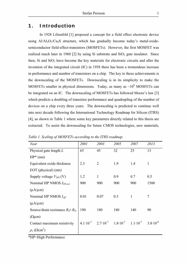
[4], as shown in Table 1 where some key parameters directly related to this thesis are
extracted. To assist the downscaling for future CMOS technologies, new materials,
Table 1. Scaling of MOSFETs according to the ITRS roadmap.
Year 2001 2003 2005 2007 2013
Physical gate length L
HP* (nm)
65 45 32 25 13
Equivalent oxide thickness
EOT (physical) (nm)
2.3 2 1.9 1.4 1
Supply voltage VDD (V) 1.2 1 0.9 0.7 0.5
Nominal HP NMOS IDS,sat
(µA/µm)
900 900 900 900 1500
Nominal HP NMOS Ioff
(µA/µm)
0.01 0.07 0.3 1 7
Source/drain resistance RS+RD
(Ωµm)
190 180 180 140 90
Contact maximum resistivity
ρc (Ωcm2)
4.1·10-7 2.7·10-7 1.8·10-7 1.1·10-7 3.8·10-8
*HP=High Performance
Modeling and characterization of novel MOS device structures
2
notably high-κ dielectric, strained Si/Si1-xGex, metal gate and NiSi contact, are being
incorporated in the MOSFETs. Such an attempt is often referred to as “material-
scaling”, giving an extra dimension for the realization of future advanced devices.
General review articles concerning the downscaling, new materials, and innovative
device structures are available in the open literature [5-7]. In particular, the physical
gate length L is reduced in order to increase speed. At the same time the supply
voltage, VDD is reduced in order to limit the increases in power consumption and
electric fields. The saturation current, Isat is kept constant, and it only allows for a
small increase in the leakage current, Ioff.
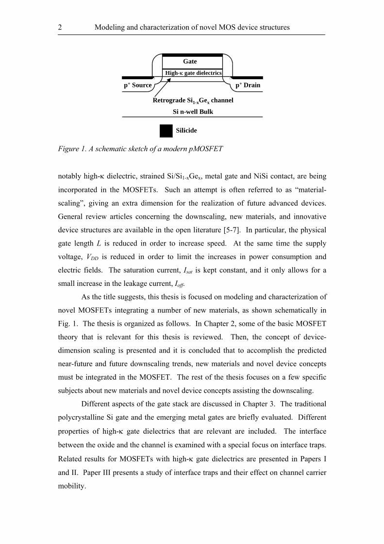
As the title suggests, this thesis is focused on modeling and characterization of
novel MOSFETs integrating a number of new materials, as shown schematically in
Fig. 1. The thesis is organized as follows. In Chapter 2, some of the basic MOSFET
theory that is relevant for this thesis is reviewed. Then, the concept of device-
dimension scaling is presented and it is concluded that to accomplish the predicted
near-future and future downscaling trends, new materials and novel device concepts
must be integrated in the MOSFET. The rest of the thesis focuses on a few specific
subjects about new materials and novel device concepts assisting the downscaling.
Different aspects of the gate stack are discussed in Chapter 3. The traditional
polycrystalline Si gate and the emerging metal gates are briefly evaluated. Different
properties of high-κ gate dielectrics that are relevant are included. The interface
between the oxide and the channel is examined with a special focus on interface traps.
Related results for MOSFETs with high-κ gate dielectrics are presented in Papers I
and II. Paper III presents a study of interface traps and their effect on channel carrier
mobility.
High-κ gate dielectrics
Retrograde Si1-xGex channel
Si n-well Bulk
p+ Drainp+ Source
Gate
Silicide
Figure 1. A schematic sketch of a modern pMOSFET
Stefan Persson 3
In Chapter 4, a description of channel engineering is provided. It starts with
an introduction to charge sheet models. A charge sheet model for MOSFETs with a
retrograde channel profile is presented. The model deals with drain current, intrinsic
charges and intrinsic capacitances. The results for Si channel MOSFETs are
presented in Papers IV and V. Since compressively strained Si1-xGex gives rise to
higher hole mobility than the usual Si channel, Si1-xGex channel pMOSFETs with a
retrograde channel profile are also examined theoretically.
Discussions about the source and drain regions in terms of contact resistance
are presented in Chapter 5. Different methods to measure specific contact resistivity
are first presented with a thorough description of the cross-bridge Kelvin (CBK)
structure. The CBK structure is modeled in both two- and three-dimensions. The
results for the traditional TiSi2-Si contact as well as for the more advanced NiSi1-xGex-
Si1-xGex contact, both obtained using the CBK structure, are presented in Papers VI
and VIII, respectively. To quantify how energy band engineering could affect a
metal-semiconductor contact, the results of the TiW-Si1-xGex contact, obtained using
another commonly used method - Transmission Line Method (TLM) are presented in
Paper VII. Finally, a short summary of this thesis is given in Chapter 6.

Modeling and characterization of novel MOS device structures
4
Stefan Persson 5
2. Operation of MOSFET
In this chapter, the basic MOSFET theory directly relevant to this thesis will
be briefly reviewed. The first section gives a description of basic MOSFET theory.
The second section describes the scaling trend and the challenges to the scaling. From
the second section, it becomes clear that “unconventional” materials and a
modification to the channel structure are necessary.
2.1 Basic MOSFET theory
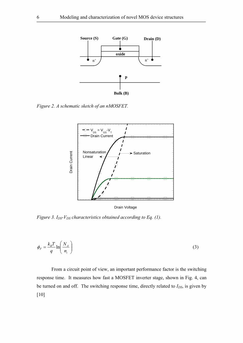
For convenience, a schematic cross-section of an n-channel MOSFET is
shown in Fig. 2. When a negative voltage is applied to the gate terminal, holes are
accumulated at the oxide-bulk interface. Between the source and drain, there are now
two diodes coupled back to back. Therefore there can be no current between these
two terminals, except for a leakage current. When a positive voltage is applied to the
gate terminal, electrons are attracted to the oxide-bulk interface by the vertical electric
field. These electrons form an n-type channel between the source and drain, where
they can flow from the source to the drain under the influence of a lateral electric
field. Under this condition, the drain current [8] can be expressed as
( )
( )
⎪⎪⎪
⎩
⎪⎪⎪
⎨
⎧
<
>−>−
>−≤⎥⎦⎤
⎢⎣⎡ −−
=
TGS
TGSTGSDSTGS
ox
TGSTGSDSDSDSTGSox
DS
VV
VVVVVVV
CL
W
VVVVVVVVVCL
W
I
0
2
21
2
2
µ
µ
(1)
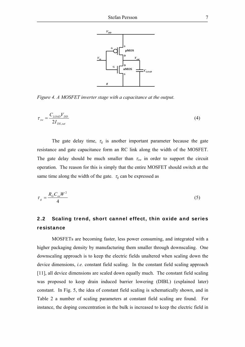
How IDS varies with VDS is schematically shown in Fig. 3. The voltage on the gate
terminal needed to create a strong inversion in the channel is called threshold voltage,
VT. For a uniformly doped substrate, VT [9] is determined by
ox
FASiF
ox
fmsT C
qNCQ
Vφε
φφ4
2 ++′
−= (2)
where
Modeling and characterization of novel MOS device structures
6
⎟⎟⎠
⎞⎜⎜⎝
⎛=
i
ABF n
NqTk lnφ (3)
From a circuit point of view, an important performance factor is the switching
response time. It measures how fast a MOSFET inverter stage, shown in Fig. 4, can
be turned on and off. The switching response time, directly related to IDS, is given by
[10]
Source (S) Gate (G) Drain (D)
Bulk (B)
p
n+ n+
oxide
Figure 2. A schematic sketch of an nMOSFET.
VDS
= VGS
-VT
Drain Current
Dra
in C
urre
nt
Drain Voltage
SaturationNonsaturationLinear
Figure 3. IDS-VDS characteristics obtained according to Eq. (1).
Stefan Persson 7
satDS
DDLOADsw I
VC
,2=τ (4)
The gate delay time, τg is another important parameter because the gate
resistance and gate capacitance form an RC link along the width of the MOSFET.
The gate delay should be much smaller than τsw in order to support the circuit
operation. The reason for this is simply that the entire MOSFET should switch at the
same time along the width of the gate. τg can be expressed as
4
2WCR oxGg =τ (5)
2.2 Scaling trend, short cannel effect, thin oxide and series
resistance
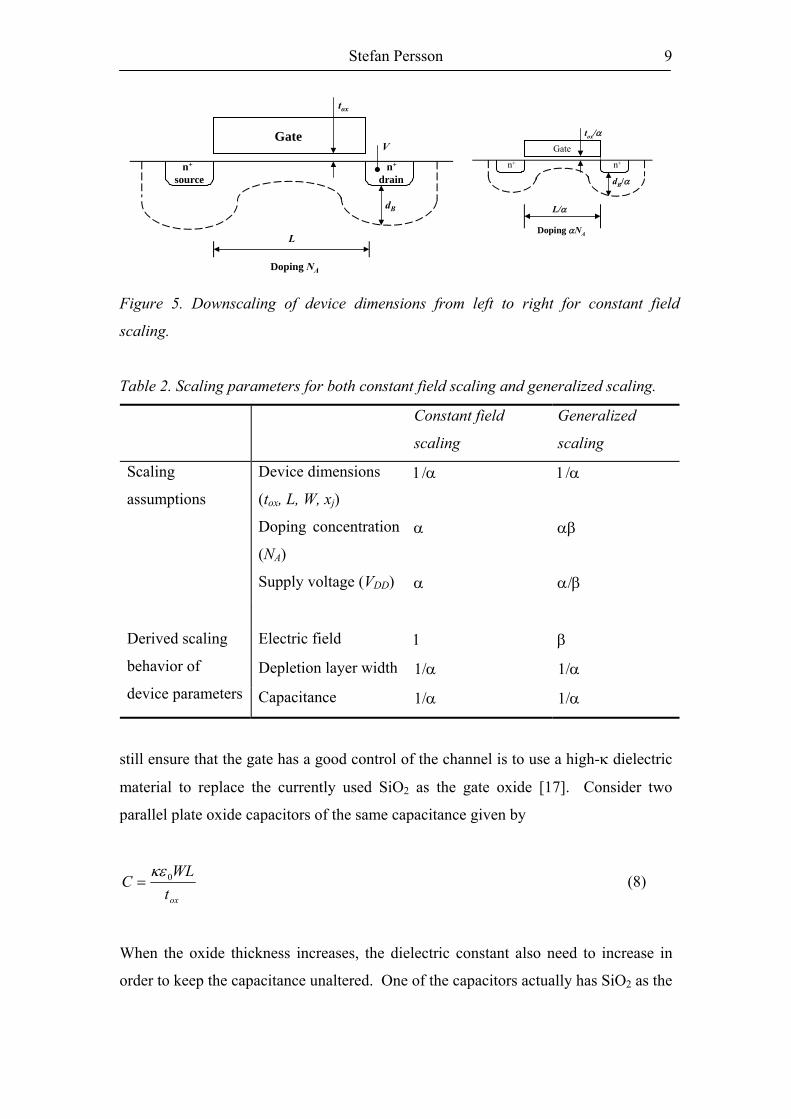
MOSFETs are becoming faster, less power consuming, and integrated with a
higher packaging density by manufacturing them smaller through downscaling. One
downscaling approach is to keep the electric fields unaltered when scaling down the
device dimensions, i.e. constant field scaling. In the constant field scaling approach
[11], all device dimensions are scaled down equally much. The constant field scaling
was proposed to keep drain induced barrier lowering (DIBL) (explained later)
constant. In Fig. 5, the idea of constant field scaling is schematically shown, and in
Table 2 a number of scaling parameters at constant field scaling are found. For
instance, the doping concentration in the bulk is increased to keep the electric field in
nMOS
pMOS
0
VDD
CLOADS
S
D
DG
G
VoutVin
Figure 4. A MOSFET inverter stage with a capacitance at the output.
Modeling and characterization of novel MOS device structures
8
the depletion region constant and to reduce depletion width. The constant field
scaling is however not always easy to realize because some parameters cannot really
be scaled properly. Notably, neither the thermal voltage nor the bandgap of Si change
with dimensional scaling. The non-scalable thermal voltage leads to a non-scalable
sub-threshold current, which in turn determines how much threshold voltage can be
scaled down. The non-scalable bandgap leads to a non-scalable built-in potential,
which, among others, determines the depletion layer width and the short channel
effect. The off-current [12] is determined by
( ) TmkqV
Box
BDSGSoff
B
T
eqTkm
LWC
qTkVVI
−
⎟⎟⎠
⎞⎜⎜⎝
⎛−=⎟⎟
⎠
⎞⎜⎜⎝
⎛>=
2
1,0 µ (6)
where
ox
FASi
CqN
mφε 4
1+= (7)
is called body-effect coefficient [12]. Because of the exponential dependence, VT
cannot be scaled down without causing a significant increase in off-current. In fact,
the off-current increases at a constant VT because Cox increases with downscaling.
Since VT cannot be scaled down as much as the physical dimensions, a limitation also
exists in downscaling of VDD because a reduction in IDS occurs when VGS-VT is
reduced. The solution is therefore to scale down VT and VDD less rapidly than the
physical dimensions. This approach is called generalized scaling [13], as seen in
Table 2 where the electric field is increased by a factor of β so that the applied
voltages are not scaled down so fast as the device dimensions.
The high electric fields can result in electric breakdown and other reliability
issues. Furthermore, the channel carrier mobility is dependent on the vertical electric
field and degrades with increasing vertical electric field [14,15]. As the gate length
decreases, tox also need to decrease in order to increase the drive current and control
DIBL. However, tox cannot be smaller than around 20 Å due to electron tunneling
[16]. The precise minimum value of tox depends of course on applications [4], high
performance or low power, analog or digital. One method to reduce gate leakage and
Stefan Persson 9
still ensure that the gate has a good control of the channel is to use a high-κ dielectric
material to replace the currently used SiO2 as the gate oxide [17]. Consider two
parallel plate oxide capacitors of the same capacitance given by
oxtWL
C 0κε= (8)
When the oxide thickness increases, the dielectric constant also need to increase in
order to keep the capacitance unaltered. One of the capacitors actually has SiO2 as the
n+
sourcen+
drain
Gate
tox
V
L
dB
Doping NA
n+ n+
Gate
tox/α
L/α
dB/α
Doping αNA
Figure 5. Downscaling of device dimensions from left to right for constant field
scaling.
Table 2. Scaling parameters for both constant field scaling and generalized scaling.
Constant field
scaling
Generalized
scaling
Scaling
assumptions
Device dimensions
(tox, L, W, xj)
1/α 1/α
Doping concentration
(NA)
α αβ
Supply voltage (VDD) α α/β
Electric field 1 β
Depletion layer width 1/α 1/α
Derived scaling
behavior of
device parameters Capacitance 1/α 1/α
Modeling and characterization of novel MOS device structures
10
oxide and the other with a high-κ dielectric. The following relation is therefore found
between these two oxide materials:
κκκ
κ−
−
= highoxhigh
SiO tEOT ,2 (9)
where EOT is the equivalent oxide thickness; it is the equivalent thickness of a SiO2
layer which gives the same capacitance as the high-κ gate dielectric of a much larger
thickness tox,high-κ. Therefore, a high-κ gate dielectric can be thicker than a SiO2 gate
dielectric and still give rise to an equally large capacitance.
The DIBL is caused [18] by the depletion regions around the drain and the
source as shown in Fig. 6. When the gate length becomes shorter, the depletion
regions constitute a relatively larger portion of the channel. Therefore, the fraction of
the bulk charge controlled by the gate decreases while that controlled by the drain
increases. Consequently, the gate voltage needed to create a strong inversion
becomes smaller leading to a decrease in VT. Eq. (2) can be rewritten as
ox
BF
ox
fmsT C
QCQ
V′
−+′
−= φφ 2 (10)
Now, it is clear that VT decreases with decreasing BQ′ , because BQ′ is negative. The
reduction in VT is a 2-D problem. The 2-D problem can of course be solved with
numerical means. There also exist many different analytical approximations of this
problem. The foundation for the solution is that the fraction of the bulk charge
controlled by the gate is reduced. The result for the reduction of VT [18,19] is
SBFox
ASi
j
BjT V
CNq
xd
Lx
V +⎟⎟⎠
⎞⎜⎜⎝
⎛−+−=∆ φ
ε2
2121 (11)
with
SBFchannelg
A
SiB V
qE
qNd ++= φε
22 , (12)
Stefan Persson 11
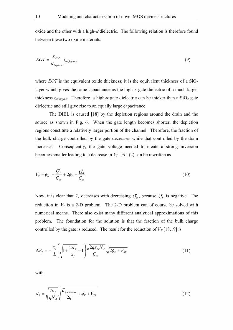
According to Eqs. (11)-(12), it is apparent that NA needs to increase and/or xj
to decrease in order to reduce the DIBL. However, NA is closely related to VT that
also needs to decrease. VT cannot be reduced below ~0.2 V because Ioff would then
become too large and thermal instability would appear [4,20]. The competing
requirements on NA for controlling DIBL and VT can be resolved with a retrograde
structure as discussed in Chapter 4. Another method to reduce the DIBL is to reduce
xj. A summary of how DIBL is affected by these parameters is shown in Table 3.
When the source and drain series resistances increase, the drain-source intrinsic
voltage decreases and therefore the drain current decreases. A high source series
resistance also reduces the gate overdrive, VGS-VT. The influence of series resistances
as well as the methods to reduce them are discussed in Chapter 5.
n+ n+
toxoxide
Source (S) Drain (D)
Gate (G)
L
xj
Bulk (B)
p
Depletion region
Figure 6. A MOSFET with the depletion regions shown. Also included are some
parameters important for scaling and DIBL.
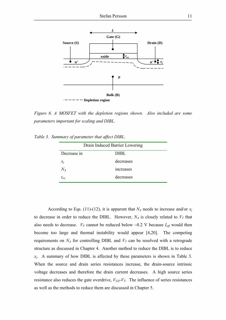
Table 3. Summary of parameter that affect DIBL.
Drain Induced Barrier Lowering
Decrease in DIBL
xj decreases
NA increases
tox decreases

Modeling and characterization of novel MOS device structures
12
Stefan Persson 13
3. Gate Stack
In this chapter the requirements for a gate stack, some of which already
mentioned in Chapter 2, will be discussed. Included are the requirements for the gate
electrode, the high-κ gate dielectrics and the interface between the dielectric and the
channel. The discussion below also refers to the appended papers, I through III.
3.1 Metal and semiconductor as gate material
Metal gates [21,22] are anticipated to replace the prevailing poly-Si(Si1-xGex)
gate in order to suppress the high gate resistance and poly-gate depletion. Poly-gate
depletion increases the EOT in inversion when p+ and n+ poly-Si are, respectively,
used for pMOSFET and nMOSFET. The dual poly-Si gates are needed for correct VT
for both types of MOSFETs. The basic requirements on a new gate material are,
among others, appropriate work function, low resistivity, chemical stability with the
surrounding materials (oxide and metallization), and process compatibility. The
depletion into a poly-Si gate [23] is calculated by
gateSi
Boxdepl Nq
Tkt 2
8ε
ε= (13)
The threshold voltage is strongly dependent on the work function of the gate
material as in Eq. (2). To achieve a proper threshold voltage for both nMOSFET and
pMOSFET, it is necessary to use two different gate metals [21] or a metal whose
work function can be tailored with doping as with poly-Si. The sheet resistance of the
gate material determines the gate resistance and therefore gate delay, τg. It is
therefore important to use a gate material with a low resistivity. Using metal gates
may also yield a lower sheet resistance than silicided poly-Si(Si1-xGex) gates give.
3.2 High-κ gate dielectrics
High-κ gate dielectrics [17] are used to achieve a small EOT and at the same
time a small gate leakage current. It is anticipated that high-κ gate dielectrics will
replace SiO2 as the gate dielectric for sub 53 nm MOSFETs aimed for digital
applications [4]. There are a number of requirements for a new gate dielectric
Modeling and characterization of novel MOS device structures
14
material, such as permittivity, bandgap, band alignment to Si, thermal stability, film
morphology, interface quality, compatibility with the current or expected materials to
be used in processing for CMOS devices, process compatibility, and reliability.
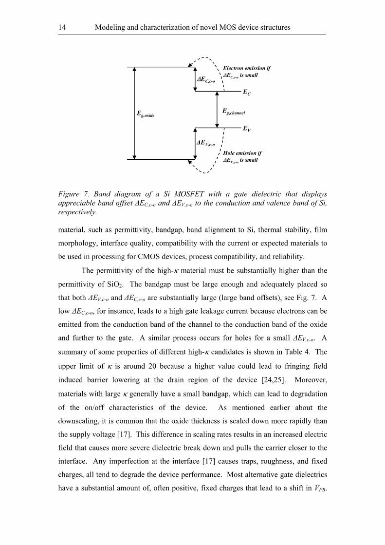
The permittivity of the high-κ material must be substantially higher than the
permittivity of SiO2. The bandgap must be large enough and adequately placed so
that both ∆EV,c-o and ∆EC,c-o are substantially large (large band offsets), see Fig. 7. A
low ∆EC,c-o, for instance, leads to a high gate leakage current because electrons can be
emitted from the conduction band of the channel to the conduction band of the oxide
and further to the gate. A similar process occurs for holes for a small ∆EV,c-o. A
summary of some properties of different high-κ candidates is shown in Table 4. The
upper limit of κ is around 20 because a higher value could lead to fringing field
induced barrier lowering at the drain region of the device [24,25]. Moreover,
materials with large κ generally have a small bandgap, which can lead to degradation
of the on/off characteristics of the device. As mentioned earlier about the
downscaling, it is common that the oxide thickness is scaled down more rapidly than
the supply voltage [17]. This difference in scaling rates results in an increased electric
field that causes more severe dielectric break down and pulls the carrier closer to the
interface. Any imperfection at the interface [17] causes traps, roughness, and fixed
charges, all tend to degrade the device performance. Most alternative gate dielectrics
have a substantial amount of, often positive, fixed charges that lead to a shift in VFB.
Eg,oxideEg,channel
∆EC,c-o
∆EV,c-o
EC
EV
Electron emission if ∆EC,c-o is small
Hole emission if ∆EV,c-o is small
Figure 7. Band diagram of a Si MOSFET with a gate dielectric that displays appreciable band offset ∆EC,c-o and ∆EV,c-o to the conduction and valence band of Si, respectively.
Stefan Persson 15
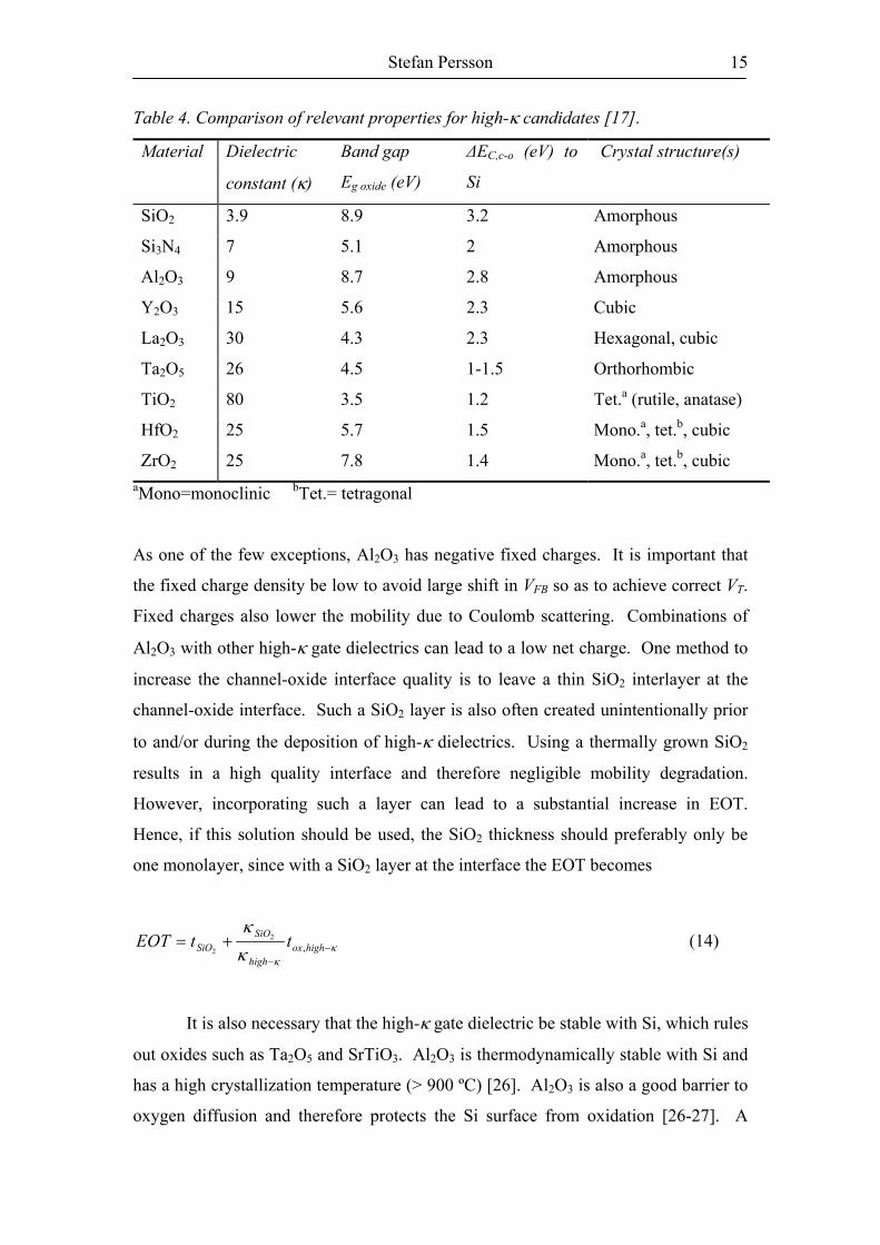
As one of the few exceptions, Al2O3 has negative fixed charges. It is important that
the fixed charge density be low to avoid large shift in VFB so as to achieve correct VT.
Fixed charges also lower the mobility due to Coulomb scattering. Combinations of
Al2O3 with other high-κ gate dielectrics can lead to a low net charge. One method to
increase the channel-oxide interface quality is to leave a thin SiO2 interlayer at the
channel-oxide interface. Such a SiO2 layer is also often created unintentionally prior
to and/or during the deposition of high-κ dielectrics. Using a thermally grown SiO2
results in a high quality interface and therefore negligible mobility degradation.
However, incorporating such a layer can lead to a substantial increase in EOT.
Hence, if this solution should be used, the SiO2 thickness should preferably only be
one monolayer, since with a SiO2 layer at the interface the EOT becomes
κκκ
κ−
−
+= highoxhigh
SiOSiO ttEOT ,
2
2 (14)
It is also necessary that the high-κ gate dielectric be stable with Si, which rules
out oxides such as Ta2O5 and SrTiO3. Al2O3 is thermodynamically stable with Si and
has a high crystallization temperature (> 900 ºC) [26]. Al2O3 is also a good barrier to
oxygen diffusion and therefore protects the Si surface from oxidation [26-27]. A
Table 4. Comparison of relevant properties for high-κ candidates [17].
Material Dielectric
constant (κ)
Band gap
Eg oxide (eV)
∆EC,c-o (eV) to
Si
Crystal structure(s)
SiO2 3.9 8.9 3.2 Amorphous
Si3N4 7 5.1 2 Amorphous
Al2O3 9 8.7 2.8 Amorphous
Y2O3 15 5.6 2.3 Cubic
La2O3 30 4.3 2.3 Hexagonal, cubic
Ta2O5 26 4.5 1-1.5 Orthorhombic
TiO2 80 3.5 1.2 Tet.a (rutile, anatase)
HfO2 25 5.7 1.5 Mono.a, tet.b, cubic
ZrO2 25 7.8 1.4 Mono.a, tet.b, cubic aMono=monoclinic bTet.= tetragonal
Modeling and characterization of novel MOS device structures
16
drawback with Al2O3 is its relatively low dielectric constant. HfO2 has a considerably
higher dielectric constant. Its main drawbacks are a low crystallization temperature
(below 400 oC), interfacial reactions at the HfO2/Si interface and growth of interfacial
layers [28-29]. HfO2 also features a poor barrier to oxygen diffusion. Crystallization
can lead to a high leakage current and a less uniform and reproducible dielectric, as
compared to an amorphous material with otherwise equivalent properties. The reason
for a high leakage current is likely due to the presence of grain boundaries in the HfO2
layer that generate states located in the bandgap of the HfO2. The decrease in
uniformity and reproducibility is likely caused by differences in κ that is different for
different crystallographic structures of HfO2. Local thinning of the HfO2 layer upon
crystallization may also occur preferably at the grain boundaries due to grain
grooving. A possible solution to achieving a low EOT, a low leakage, and a good
barrier to oxygen diffusion (and therefore protects the Si surface to the channel and
the gate electrode material) is to use a tri-layer nano-laminate gate oxide stack such as
Al2O3/HfO2/Al2O3. This proof-of-concept structure motivated the work summarized
in Papers I through III.
Si pMOSFETs with Al2O3 as gate oxide were studied by Ragnarsson et. al.
[30]. They extracted a degraded hole mobility. The mobility degradation was
attributed to Coulomb scattering by the high density of interface traps (low 1011 cm-
2eV-1). Shi et. al. [31] studied pMOSFETs with both Si and Si0.8Ge0.2 channels where
HfO2 was used as the gate dielectric. The sub-threshold slope was found to be 85 and
105 mV/dec for the Si and Si0.8Ge0.2 device, respectively. The corresponding EOT
was 2.1 and 2.4 nm. This difference in sub-threshold behavior was explained as
resulting from differences in density of interface states as well as in EOT. Bae et. al.
[32] studied nMOSFETs with AlHfOx as gate oxide with an EOT equal to 2.8 nm.
The crystallization temperature of the AlHfOx layer was found to increase with
decreasing Hf content. The sub-threshold slope was 73 and 72 mV/dec for 20 and 38
at. % Al, respectively.
Our Si0.7Ge0.3 pMOSFET with Al2O3/HfAlOx/Al2O3, Al2O3/HfO2/Al2O3, and
Al2O3 dielectrics displayed a sub-threshold slope of 110, 110, 135 mV/dec,
respectively, see Papers I and II. The Si pMOSFET with the Al2O3/HfAlOx/Al2O3
stack exhibited a sub-threshold slope of 75 mV/dec. An EOT of 2.3, 2.8, and 3.4 nm
was extracted for the Si0.7Ge0.3 pMOSFET with Al2O3/HfO2/Al2O3,
Stefan Persson 17
Al2O3/HfO2/Al2O3, and Al2O3, respectively. It is however hard to directly compare
our pMOSFETs with those of Ragnarsson et. al., because no sub-threshold slope was
specified in their work. Since our Si pMOSFET with EOT=2.8 nm exhibited an
appreciably lower sub-threshold slope (75 mV/dec) than in the MOSFET of Shi et. al.
with EOT=2.1 nm (85 mV/dec), the interface quality of our Si device should be
better. For the SiGe devices, both the sub-threshold slope and the EOT are
comparable although we had a larger Ge content than theirs (30 at.% vs. 20 at.%).
Finally, it is difficult to make a fair comparison between our pMOSFETs with the
nMOSFETs of Bae et. al. Examples of other studies of MOSFET with high-k gate
dielectrics can be found in [33-35].
3.3 Gate oxide-channel interface and interface traps
The interface between gate oxide and channel is a crucial component of a
MOSFET. The electrons are very closely bound to this interface because of the high
vertical electric field. Imperfections at the interface can cause carrier trapping,
mobility degradation, and change of threshold voltage. Carriers trapped at the
interface are named interface trapped charges [36]. Interface traps can be a result of
structural defects, metal impurities, or other defects caused by radiation or similar
bond-breaking process. Since these traps are in electrical communication with the
semiconductor, they can both trap and de-trap a carrier in the semiconductor.
Depending on the nature of the trap as well as the Fermi level and bias condition, the
trap can be positive, negative, or neutral. These traps can also lead to increases in
sub-threshold slope and decreases in carrier mobility due to increased Coulomb
scattering. Studies of interface traps in a MOS structure have been an important
subject [37,38] and can be traced back in early semiconductor research [39]. Si
channel MOSFET with thermally grown SiO2 gate dielectrics usually has a low
density of interface traps. However, MOS structures with SiGe channel and/or high-κ
gate dielectrics often show a high density of interface traps.
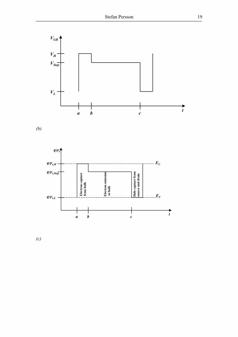
Density of interface traps, Dit can be measured with several different
techniques. One of them is three-level charge-pumping [40]. Three-level charge-
pumping can measure both the density of interface traps and the energy position of the
traps in the bandgap. The following is a short description of how the measurement
actually works. When a voltage pulse on the gate drives the surface into accumulation
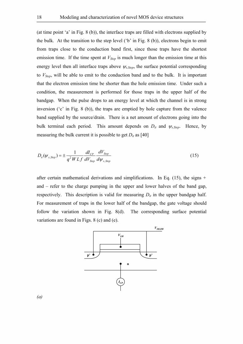
Modeling and characterization of novel MOS device structures
18
(at time point ‘a’ in Fig. 8 (b)), the interface traps are filled with electrons supplied by
the bulk. At the transition to the step level (‘b’ in Fig. 8 (b)), electrons begin to emit
from traps close to the conduction band first, since those traps have the shortest
emission time. If the time spent at VStep is much longer than the emission time at this
energy level then all interface traps above ψs,Step, the surface potential corresponding
to VStep, will be able to emit to the conduction band and to the bulk. It is important
that the electron emission time be shorter than the hole emission time. Under such a
condition, the measurement is performed for those traps in the upper half of the
bandgap. When the pulse drops to an energy level at which the channel is in strong
inversion (‘c’ in Fig. 8 (b)), the traps are emptied by hole capture from the valence
band supplied by the source/drain. There is a net amount of electrons going into the
bulk terminal each period. This amount depends on Dit and ψs,Step. Hence, by
measuring the bulk current it is possible to get Dit as [40]
Steps
Step
Step
CPStepsit d
dVdVdI
fLWqD
,2,
1)(ψ
ψ ±= (15)
after certain mathematical derivations and simplifications. In Eq. (15), the signs +
and – refer to the charge pumping in the upper and lower halves of the band gap,
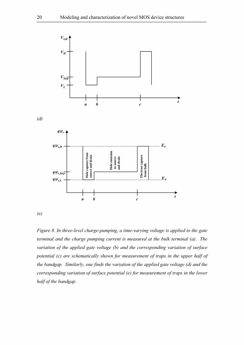
respectively. This description is valid for measuring Dit in the upper bandgap half.
For measurement of traps in the lower half of the bandgap, the gate voltage should
follow the variation shown in Fig. 8(d). The corresponding surface potential
variations are found in Figs. 8 (c) and (e).
p+ p+
ICP
n
VGB
VSB,DB
(a)
Stefan Persson 19
t
VGB
VH
VL
VStep
a b c
(b)
ta b c
qψs
Ele
ctro
n em
issi
onto
bul
k
Ele
ctro
n ca
ptur
e fr
om b
ulk
EC
EV
qψs,H
qψs,Step
qψs,L
Hol
e ca
ptur
e fr
om
sour
ce a
nd d
rain
(c)
Modeling and characterization of novel MOS device structures
20
t
VGB
VH
VL
VStep
a b c
(d)
ta b c
Hol
e ca
ptur
e fr
om
sour
ce a
nd d
rain
Hol
e em
issi
onto
sour
ce
and
drai
n
Ele
ctro
n ca
ptur
efr
om b
ulk
EC
EV
qψs
qψs,H
qψs,Step
qψs,L
(e)
Figure 8. In three-level charge-pumping, a time-varying voltage is applied to the gate
terminal and the charge pumping current is measured at the bulk terminal (a). The
variation of the applied gate voltage (b) and the corresponding variation of surface
potential (c) are schematically shown for measurement of traps in the upper half of
the bandgap. Similarly, one finds the variation of the applied gate voltage (d) and the
corresponding variation of surface potential (e) for measurement of traps in the lower
half of the bandgap.
Stefan Persson 21
3.4 Effects of interface traps on mobility and mobility
measurement
In Paper III, the extraction of effective hole mobility was performed on
pMOSFETs with a strained-Si0.7Ge0.3 surface-channel in combination with an ALD
TiN/Al2O3/HfAlOx/Al2O3 gate stack. In these devices, a high density of interface
traps on the order of 1012 cm-2eV-1 was found. As a result, a heavily distorted
effective mobility curve with a slow mobility roll-off towards low vertical electric
field was found. This distortion was mainly caused by mobility degradation as a
result of Coulomb scattering of the mobile channel carriers by the charged interface
defects, i.e. charged traps or trapped-carriers that remain charged (i.e. trapped
charges). A considerable proportion of the distortion resulted, however, from a direct
use of the standard split-CV measurement results. Since a significant fraction of the
inversion carriers became trapped at the interface, an error arose when using the
standard split-CV technique. After compensation for the trapped charges, a
substantial mobility enhancement was demonstrated with the devices, as compared to
the Si reference devices with the same gate stack as well as to the universal hole
mobility curve for Si.
Recognizing the potential detrimental effect of charge trapping on the mobility
extraction using the standard split-CV technique, a procedure for extraction of correct
mobility was presented in Paper III. In our approach there, the trapped, immobile
charge was first found by counting the traps measured by charge-pumping over an
appropriate energy/voltage interval. The effective mobility was then calculated using
the Split-CV method after removing the immobile charge from the measured QI curve
using CV technique. In short, our approach examined the charges. An alternative
method is to make the compensation on the Cgc curve, i.e. to examine the
capacitances. It is shown below that these two approaches are entirely equivalent, as
expected.
If trapping and de-trapping of carriers can follow the small AC signal in the
CV measurement, the density of inversion carriers measured by means of the split-CV
method consists of two components in the presence of interface traps,
immobImobII QQQ ,, += (16)
Modeling and characterization of novel MOS device structures
22
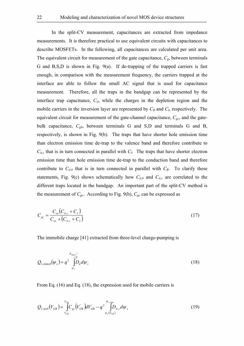
In the split-CV measurement, capacitances are extracted from impedance
measurements. It is therefore practical to use equivalent circuits with capacitances to
describe MOSFETs. In the following, all capacitances are calculated per unit area.
The equivalent circuit for measurement of the gate capacitance, Cg, between terminals
G and B,S,D is shown in Fig. 9(a). If de-trapping of the trapped carriers is fast
enough, in comparison with the measurement frequency, the carriers trapped at the
interface are able to follow the small AC signal that is used for capacitance
measurement. Therefore, all the traps in the bandgap can be represented by the
interface trap capacitance, Cit, while the charges in the depletion region and the
mobile carriers in the inversion layer are represented by CB and CI, respectively. The
equivalent circuit for measurement of the gate-channel capacitance, Cgc, and the gate-
bulk capacitance, Cgb, between terminals G and S,D and terminals G and B,
respectively, is shown in Fig. 9(b). The traps that have shorter hole emission time
than electron emission time de-trap to the valence band and therefore contribute to
Cit,c that is in turn connected in parallel with CI. The traps that have shorter electron
emission time than hole emission time de-trap to the conduction band and therefore
contribute to Cit,b that is in turn connected in parallel with CB. To clarify these
statements, Fig. 9(c) shows schematically how Cit,b and Cit,c are correlated to the
different traps located in the bandgap. An important part of the split-CV method is
the measurement of Cgc. According to Fig. 9(b), Cgc can be expressed as
( )( )Icitox
Icitoxgc CCC
CCCC
++
+=
,
, (17)
The immobile charge [41] extracted from three-level charge-pumping is
( ) ∫=q
E
sitsimmobI
s
dDqQ
max
2,
ψ
ψψ (18)
From Eq. (16) and Eq. (18), the expression used for mobile carriers is
( ) ( )( )∫∫ −=max,
,2''
,
s
GBs
FB
GB Vscit
V
VGBGBgcGBmobI dDqdVVCVQ
ψ
ψ
ψ (19)

Stefan Persson 23
The relation between Dit,c and Cit,c is [41]
citcit DqC ,2
, = (20)
Inserting Eq. (20) in Eq. (19) gives
( ) ( )( )∫∫ −=max,
,''
,
s
GBs
FB
GB Vscit
V
VGBGBgcGBmobI dCdVVCVQ
ψ
ψ
ψ (21)
The inversion charge in the equivalent circuit in Fig. 9(b) is given by
Cox
CICB Cit
G
B,S,D
ψs
B S,D
Cox
CICB Cit,b
G
Cit,c
ψs
(a) (b)
Emax
Cit
EV EC E
Cit,c Cit,b
(c)
Figure 9. Equivalent circuits for measurement of Cgg (a) and measurements of Cgc and
Cgb (b), as well as correlation of Cit,b and Cit,c to the different traps located in the
bandgap (c).
Modeling and characterization of novel MOS device structures
24
( ) ∫=FBs
s
sIsmobI dCQ,
,
ψ
ψ
ψψ (22)
which can be rewritten as:
( ) ( ) ∫∫ −+=FBs
s
FBs
s
scitscitIsmobI dCdCCQ,,
,,,
ψ
ψ
ψ
ψ
ψψψ (23)
From Fig. 9(b) the relation between VGB and ψs is
( ) GBIcitox
oxs dV
CCCC
d++
=,
ψ (24)
using that VCB=0. Inserting Eq. (24) and Eq. (17) in Eq. (23) yields
( ) ( )( )∫∫ −=
FBs
GBs
FB
GB Vscit
V
VGBGBgcGBmobI dCdVVCVQ
,
,''
,
ψ
ψ
ψ (25)
Since there exists no interface trap in communication with the inversion
charge between ψs,FB and ψs,max, Eq. (25) is in fact identical to Eq. (21). Furthermore,
it has shown slightly earlier that Eq. (21) is equivalent to Eq. (19). The latter equation
is used in Paper III.
Stefan Persson 25
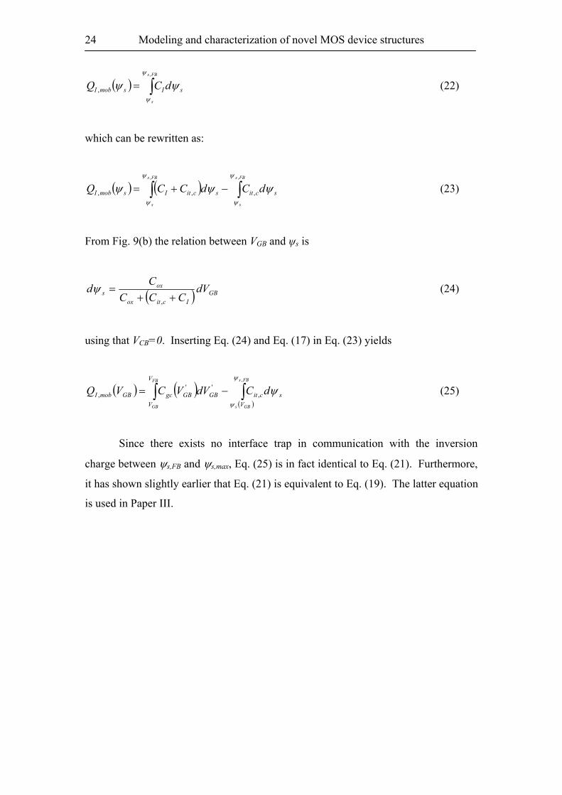
4. Channel Structure
Different designs for the channel of a MOSFET are discussed in this chapter.
A retrograde channel is used to reduce the short channel effect at a given threshold
voltage, whereas a Si1-xGex channel is used to improve the performance of
pMOSFETs (higher current). This chapter begins with a charge sheet model that most
models today are based on. Extensive results related to the retrograde channel are
presented in Papers IV and V. Since retrograde Si1-xGex channels are found in Papers
I and II, an extension is made of the charge sheet model developed in Papers IV and V
to account for the influence of the retrograde Si1-xGex channels.
4.1 Charge sheet model
Charge sheet models [42-44] can be used for calculation of drain current,
charges, and capacitances in MOSFETs. The models are superior to threshold voltage
models because of their general validity in all regions of inversion. For MOSFETs
with uniformly doped bodies (i.e. substrates, where the channel is found), analytical
solutions of drain current, charge, and capacitances expressed as functions of surface
potential have been developed. The basic assumptions in the charge sheet models are
that the inversion layer has an infinitesimal thickness and that the drain current is
caused by drift and diffusion. With these assumptions the surface potential, for an
nMOSFET, is given by
t
V
tssFBGBt
CBFs
eVV φφψγψ φφψ
−+++=−−2
(26)
with
ox
ASi
CNqε
γ2
= (27)
There also exist analytical approximations to Eq. (26) [45,46]. The inversion
charge can be expressed as a function of surface potential by assuming a gradual
channel from source to drain in the lateral direction and using the depletion
approximation. The result is
Modeling and characterization of novel MOS device structures
26
( )tssFBGBoxI VVCQ φψγψ −−−−−=′ (28)
By assuming steady state and constant mobility, IDS is given by
( ) ( )∫ ′−′+′−=sL
s
IILtsIDS QQdQL
WIψ
ψ
φψµ0
0 (29)
4.2 Retrograde channel
A common doping profile in the channel of modern MOSFETs is a retrograde
one [47] with a lightly doped surface layer on top of a relatively heavily doped
substrate. Such a profile aims at controlling the short channel effect and achieving an
acceptable threshold voltage. The retrograde structure is shown in Figs. 10(a) and (b).
The low surface doping concentration can also increase the effective mobility by
reducing the Coulomb scattering in the channel. Our mathematical analysis of the
retrograde channel in Paper IV gives some revealing results for surface potential and
capacitances. A strikingly simple relation between ψs and ψξ, the potential at the
interface between the intrinsic surface layer and the doped substrate, is derived as
∆−−∆+=− tst φψφψ ξ (30)
with
2
2ξ
ε Si
AqN=∆ (31)
It leads to another important result with a simple change in bulk charge upon
implementation of a retrograde channel. In a uniformly doped channel, the bulk
charge per unit area is
tsoxB CQ φψγ −−=′ (32)
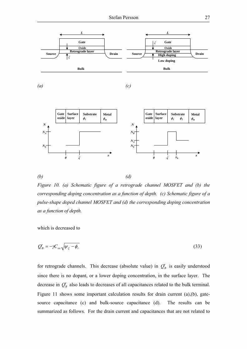
Stefan Persson 27
which is decreased to
toxB CQ φψγ ξ −−=′ (33)
for retrograde channels. This decrease (absolute value) in BQ′ is easily understood
since there is no dopant, or a lower doping concentration, in the surface layer. The
decrease in BQ′ also leads to decreases of all capacitances related to the bulk terminal.
Figure 11 shows some important calculation results for drain current (a),(b), gate-
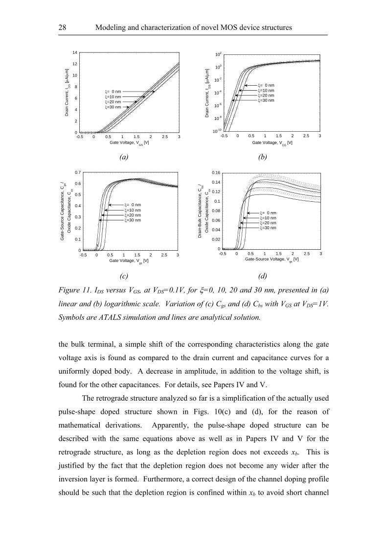
source capacitance (c) and bulk-source capacitance (d). The results can be
summarized as follows. For the drain current and capacitances that are not related to
ξ
L
Oxide
Source Drain
Gate
Retrograde layer
Bulk
ξ
L
Oxide
Source Drain
Gate
Retrograde layer
Bulk
High doping
Low doping
(a)
(c)
Gate oxide
Surface layer
Substrateφ1
x0 ξ
N
NA
NS
Metalφm
Gate oxide
Surface layer
Substrateφ1 φ2
x0 ξ
N
NB
NS
NA
xb
Metalφm
(b) (d)
Figure 10. (a) Schematic figure of a retrograde channel MOSFET and (b) the
corresponding doping concentration as a function of depth. (c) Schematic figure of a
pulse-shape doped channel MOSFET and (d) the corresponding doping concentration
as a function of depth.
Modeling and characterization of novel MOS device structures
28
the bulk terminal, a simple shift of the corresponding characteristics along the gate
voltage axis is found as compared to the drain current and capacitance curves for a
uniformly doped body. A decrease in amplitude, in addition to the voltage shift, is
found for the other capacitances. For details, see Papers IV and V.
The retrograde structure analyzed so far is a simplification of the actually used
pulse-shape doped structure shown in Figs. 10(c) and (d), for the reason of
mathematical derivations. Apparently, the pulse-shape doped structure can be
described with the same equations above as well as in Papers IV and V for the
retrograde structure, as long as the depletion region does not exceeds xb. This is
justified by the fact that the depletion region does not become any wider after the
inversion layer is formed. Furthermore, a correct design of the channel doping profile
should be such that the depletion region is confined within xb to avoid short channel
0
2
4
6
8
10
12
14
-0.5 0 0.5 1 1.5 2 2.5 3
Dra
in C
urre
nt, I
DS [µ
A/µ
m]
Gate Voltage, VGS
[V]
ξ= 0 nm
ξ=20 nmξ=30 nm
ξ=10 nm
10-10
10-8
10-6
10-4
10-2
100
102
-0.5 0 0.5 1 1.5 2 2.5 3
Dra
in C
urre
nt, I
DS [µ
A/µm
]
Gate Voltage, VGS
[V]
ξ= 0 nm
ξ=20 nmξ=30 nm
ξ=10 nm
(a) (b)
0
0.1
0.2
0.3
0.4
0.5
0.6
0.7
-0.5 0 0.5 1 1.5 2 2.5 3
Gat
e-So
urce
Cap
acita
nce,
Cgs
/O
xide
Cap
acita
nce,
Cox
Gate Voltage, Vgs
[V]
ξ= 0 nm
ξ=20 nmξ=30 nm
ξ=10 nm
0
0.02
0.04
0.06
0.08
0.1
0.12
0.14
0.16
-0.5 0 0.5 1 1.5 2 2.5 3
Dra
in-B
ulk
Cap
acita
nce,
Cbs
/
Oxi
de C
apac
itanc
e, C
ox
Gate-Source Voltage, Vgs
[V]
ξ= 0 nm
ξ=20 nmξ=30 nm
ξ=10 nm
(c) (d)
Figure 11. IDS versus VGS, at VDS=0.1V, for ξ=0, 10, 20 and 30 nm, presented in (a)
linear and (b) logarithmic scale. Variation of (c) Cgs and (d) Cbs with VGS at VDS=1V.
Symbols are ATALS simulation and lines are analytical solution.
Stefan Persson 29
effect. Hence, NA in the retrograde structure should correspond to the highest doping
concentration in the pulse-shape doped structure. The relatively lowly doped bulk
with NB, Fig. 10(d), does not influence the drain current and intrinsic capacitances
discussed in Papers IV and V, although it does affect the (extrinsic) junction
capacitances. This behavior is easily explained [48]: when there are several contact
potentials in series, it is their sum that is of importance in accordance with
Kirschhoff’s potential law. The contact potential between the substrate and the metal
in the bulk contact, in the retrograde structure, is expressed as
mm φφφ −= 1,1 (34)
The contact potential for the pulse shaped structure is identically given by:
( ) ( ) mmm φφφφφφφ −=−−−= 1221,1 (35)
Although the 1-D model described above as well as in Papers IV and V has
been developed for long-channel transistors with the retrograde channel profile
varying along the depth of the transistor, it should be applicable for short-channel
transistors as long as the short channel effects are perfectly controlled.
4.3 Si1-xGex channel
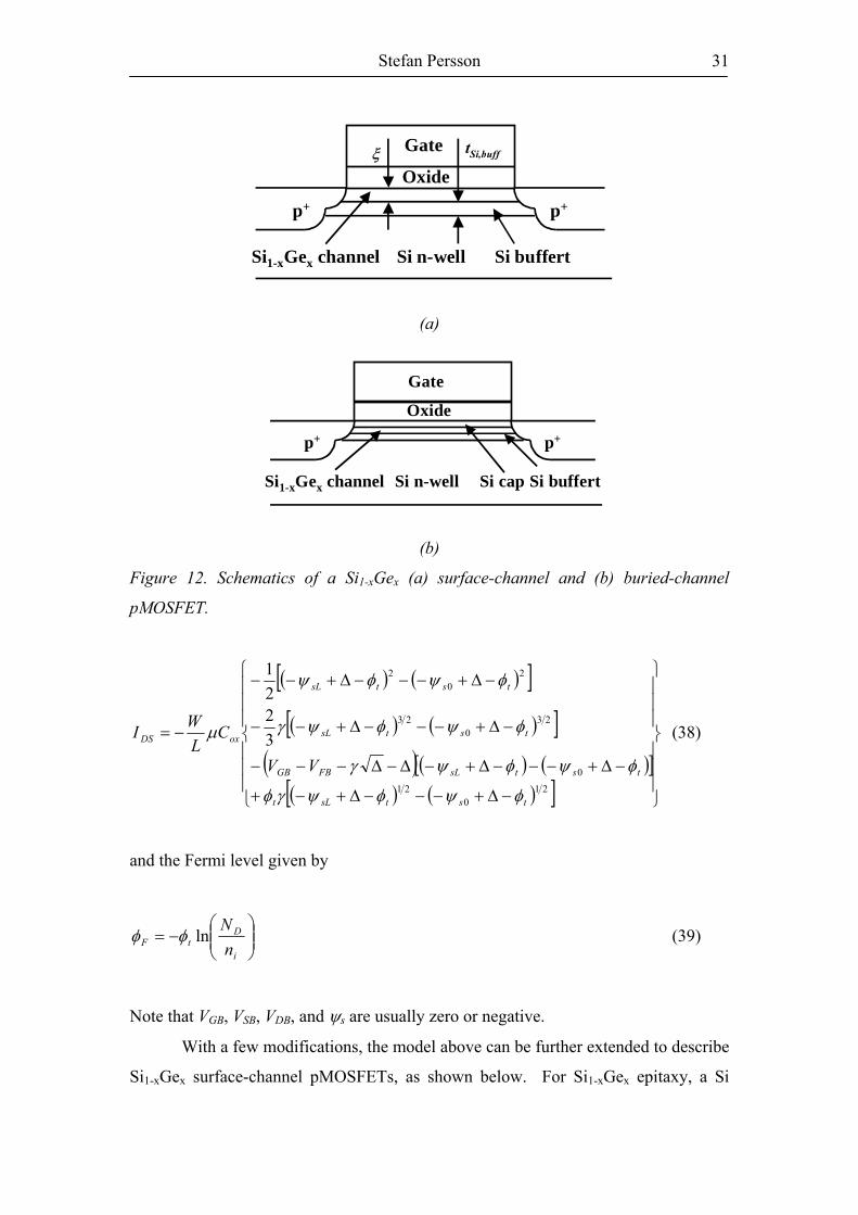
The hole mobility is considerably smaller the electron mobility in Si. This
makes the drive current, per unit gate width, of pMOSFETs smaller than that of
nMOSFETs. The gate delay is, as a result, larger for pMOSFETs than for equally
sized nMOSFETs. Incorporating a Si1-xGex-channel in pMOSFETs [49,50] can
benefit from an enhanced hole mobility in compressively strained Si1-xGex epitaxially
grown on Si substrate. To avoid a high density of interface states introduced as a
result of direct oxidation of the Si1-xGex in order to grow the SiO2 gate dielectric [51],
a Si cap-layer is often deposited on top of the strained Si1-xGex making the absolute
majority of the fabricated Si1-xGex pMOSFETs buried-channel type. Skipping the Si
cap results in Si1-xGex surface-channel pMOSFETs as shown in Chapter 3 as well as
in Papers I to III. Both types of p-type Si1-xGex MOSFETs are shown in Fig. 12.
Modeling and characterization of novel MOS device structures
30
A charge sheet model for pMOSFETs can be derived following the method for
that derived for nMOSFETs in Papers IV and V. The resultant model differs from
that for nMOSFETs with a few changes in signs, as shown below. The surface
potential equation is now expressed as
( )∆−−∆+−∆−+−−−+=+−
ts
V
ttssFBGBt
CBsF
eVV φψφφψγψ φψφ
22
(36)
where
2
2ξ
ε Si
DqN=∆ (37)
and
ox
DSi
CNqε
γ2
= (37b)
The surface potential equation at the source and drain ends can be evaluated from Eq.
(36) with VCB=VSB and VCB=VDB, respectively. The drain current is expressed as
Stefan Persson 31
( ) ( )[ ]( ) ( )[ ]
( ) ( ) ( )[ ]( ) ( )[ ] ⎪
⎪⎪
⎭
⎪⎪⎪
⎬
⎫
⎪⎪⎪
⎩
⎪⎪⎪
⎨
⎧
−∆+−−−∆+−+
−∆+−−−∆+−∆−∆−−−
−∆+−−−∆+−−
−∆+−−−∆+−−
−=
210
210
230
23
20
2
3221
tstsLt
tstsLFBGB
tstsL
tstsL
oxDS
VV
CL
WI
φψφψγφ
φψφψγ
φψφψγ
φψφψ
µ (38)
and the Fermi level given by
⎟⎟⎠
⎞⎜⎜⎝
⎛−=
i
DtF n
Nlnφφ (39)
Note that VGB, VSB, VDB, and ψs are usually zero or negative.
With a few modifications, the model above can be further extended to describe
Si1-xGex surface-channel pMOSFETs, as shown below. For Si1-xGex epitaxy, a Si
Oxide
Si1-xGex channel Si n-well
p+p+
Gate
Si buffert
ξ tSi,buff
(a)
Oxide
Si1-xGex channel Si n-well
p+p+
Si cap
Gate
Si buffert
(b)
Figure 12. Schematics of a Si1-xGex (a) surface-channel and (b) buried-channel
pMOSFET.
Modeling and characterization of novel MOS device structures
32
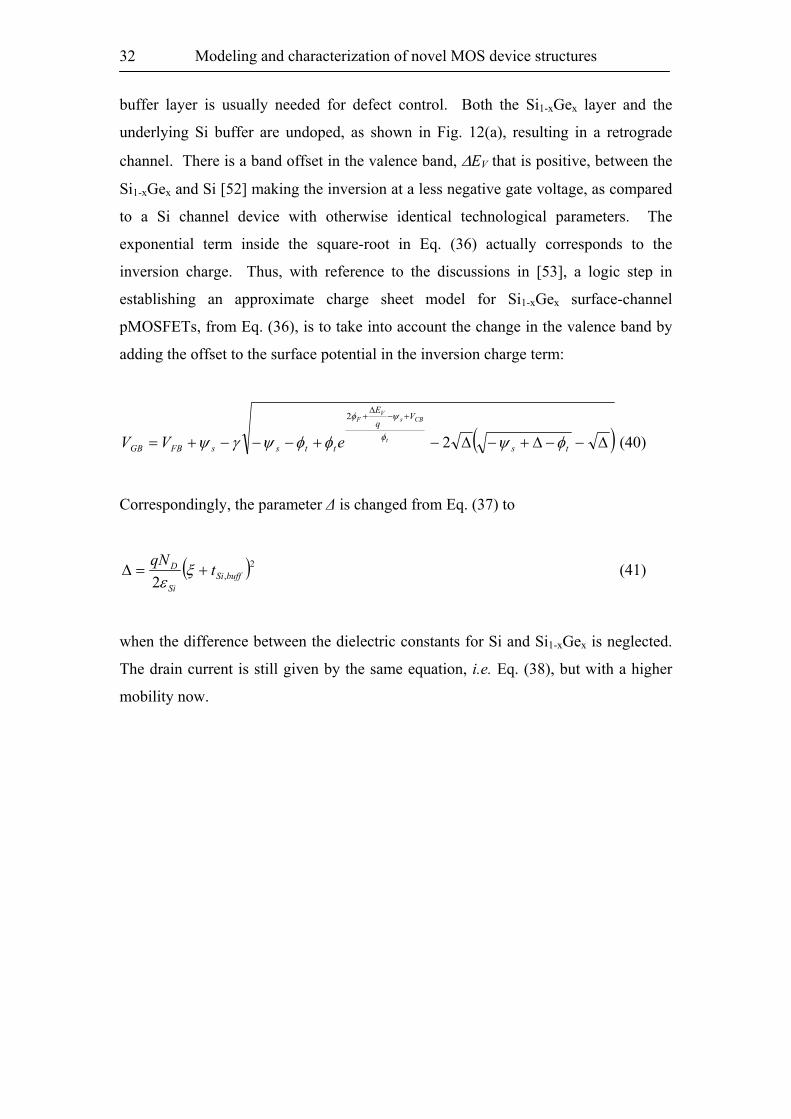
buffer layer is usually needed for defect control. Both the Si1-xGex layer and the
underlying Si buffer are undoped, as shown in Fig. 12(a), resulting in a retrograde
channel. There is a band offset in the valence band, ∆EV that is positive, between the
Si1-xGex and Si [52] making the inversion at a less negative gate voltage, as compared
to a Si channel device with otherwise identical technological parameters. The
exponential term inside the square-root in Eq. (36) actually corresponds to the
inversion charge. Thus, with reference to the discussions in [53], a logic step in
establishing an approximate charge sheet model for Si1-xGex surface-channel
pMOSFETs, from Eq. (36), is to take into account the change in the valence band by
adding the offset to the surface potential in the inversion charge term:
( )∆−−∆+−∆−+−−−+=
+−∆
+
ts
VqE
ttssFBGBt
CBsV
F
eVV φψφφψγψ φ
ψφ
2
2
(40)
Correspondingly, the parameter ∆ is changed from Eq. (37) to
( )2,2 buffSi
Si
D tqN+=∆ ξ
ε (41)
when the difference between the dielectric constants for Si and Si1-xGex is neglected.
The drain current is still given by the same equation, i.e. Eq. (38), but with a higher
mobility now.
Stefan Persson 33
5. Source and Drain Resistance
In this chapter, one of the most important extrinsic components of a MOSFET
is discussed, i.e. the specific contact resistivity between the external metallization and
the source/drain terminals. The results are found in Papers VI through VIII.
5.1 Source and drain series resistance
In a long channel MOSFET, the source and drain resistances are usually
negligible compared to the channel resistance. As the channel length is decreased,
these parasitic resistances become significant compared to the channel resistance and
can therefore cause a significant current degradation [54]. A MOSFET is mostly
affected by the source and drain resistances in the linear region where VDS is low.
In a non-silicided MOSFET with only one ion implantation of dopants to form
the source/drain junctions, as shown in Fig. 13(a), the source and drain resistances (RS
and RD) consist [55] of the following components: the accumulation layer resistance
Rac for the region where the current is confined close to the surface layer, the
spreading resistance Rsp corresponding to the transition region where the current
spreads out from the aforementioned thin layer over the depth of the source and drain,
the sheet resistance of the source and drain Rsh typically 200-500 Ω/ [56], and the
contact resistance between the source/drain terminals to the metal Rco. A
characteristic of a metal-semiconductor contact is its specific contact resistivity ρc.
Both Rsh and Rco that can severely affect the performance of a MOSFET can be
greatly reduced by using a metal silicide often formed using self-aligned silicide
(SALICIDE) technology [57]. When the SALICIDE is used, the silicide is present in
all three terminals including the gate as shown in Fig. 13(b). For a thickness of 40
nm, a silicide shunt layer typically lowers the sheet resistance to 3-5 Ω/ using C54
TiSi2, CoSi2 or NiSi with a resistivity of 10-20 µΩcm [57]. Therefore, the use of a
silicide layer is effective and crucial for reduction of the parasitic resistances. Using
silicide can also lower the specific contact resistivity, because the metal-Si contact can
be made intimate free from any interfacial contamination. A silicide with an
appropriate work function is important for low-resistivity contacts to both types of Si,
as shown in Paper VI where TiSi2 is used.
Another additional means to reduce the source/drain resistances and at the
same time to attain a small DIBL is to use two ion implantations of dopants into the
Modeling and characterization of novel MOS device structures
34
source and drain regions, forming a doping profile schematically shown in Fig. 13(b).
A low-energy implantation is first performed to form the two shallow junctions
immediately adjacent to the two ends of the channel. After the gate spacers are
formed, a relatively high energy implantation is carried out to form the deep regions
where the silicide-Si contacts are made using SALICIDE. For the source/drain
structure including a shallow and a deep profile shown in Fig. 13(b), calculation of RS
and RD is more involved than for the structure in Fig. 13(a). Numerical or
approximate analytical modeling of RS and RD can be found in [58-60].
ρsd
lc
ρc
xj
Gate
xc
S
Rco Rsh
Rsp
Rac
Metal
(a)
Silicide
Gate
n+ n+
(b)
Figure 13. MOSFET with (a) non-silicided and (b) silicided source/drains. The
different parasitic resistance components are shown in (a).
Stefan Persson 35
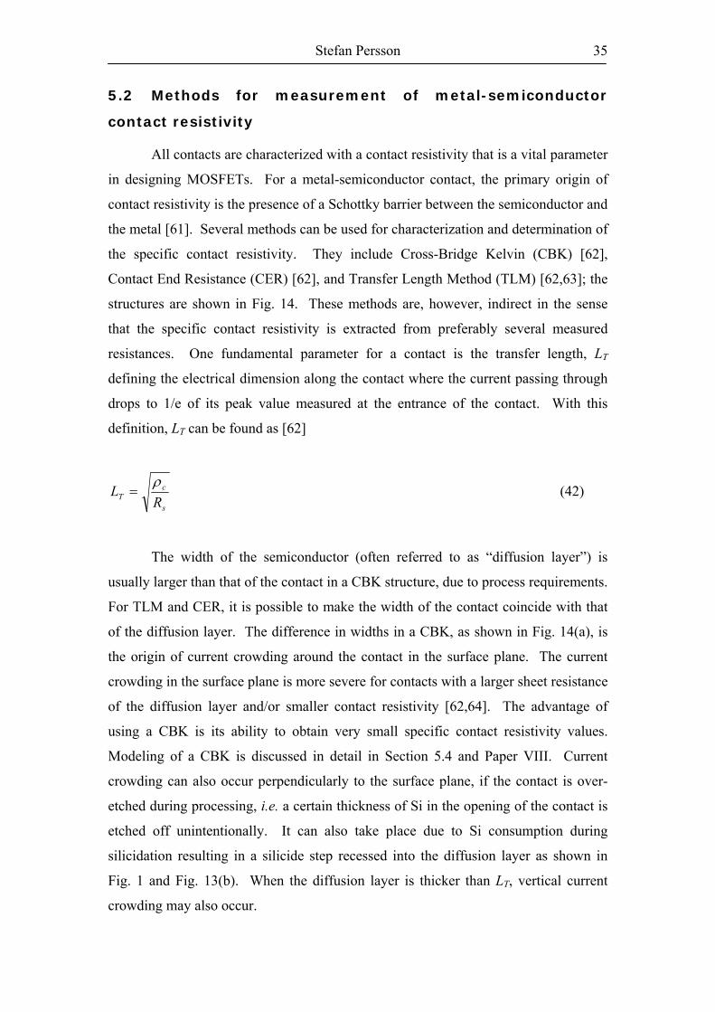
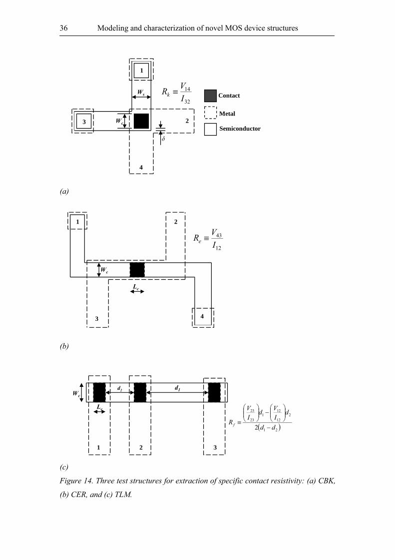
5.2 Methods for measurement of metal-semiconductor
contact resistivity
All contacts are characterized with a contact resistivity that is a vital parameter
in designing MOSFETs. For a metal-semiconductor contact, the primary origin of
contact resistivity is the presence of a Schottky barrier between the semiconductor and
the metal [61]. Several methods can be used for characterization and determination of
the specific contact resistivity. They include Cross-Bridge Kelvin (CBK) [62],
Contact End Resistance (CER) [62], and Transfer Length Method (TLM) [62,63]; the
structures are shown in Fig. 14. These methods are, however, indirect in the sense
that the specific contact resistivity is extracted from preferably several measured
resistances. One fundamental parameter for a contact is the transfer length, LT
defining the electrical dimension along the contact where the current passing through
drops to 1/e of its peak value measured at the entrance of the contact. With this
definition, LT can be found as [62]
s
cT R
Lρ
= (42)
The width of the semiconductor (often referred to as “diffusion layer”) is
usually larger than that of the contact in a CBK structure, due to process requirements.
For TLM and CER, it is possible to make the width of the contact coincide with that
of the diffusion layer. The difference in widths in a CBK, as shown in Fig. 14(a), is
the origin of current crowding around the contact in the surface plane. The current
crowding in the surface plane is more severe for contacts with a larger sheet resistance
of the diffusion layer and/or smaller contact resistivity [62,64]. The advantage of
using a CBK is its ability to obtain very small specific contact resistivity values.
Modeling of a CBK is discussed in detail in Section 5.4 and Paper VIII. Current
crowding can also occur perpendicularly to the surface plane, if the contact is over-
etched during processing, i.e. a certain thickness of Si in the opening of the contact is
etched off unintentionally. It can also take place due to Si consumption during
silicidation resulting in a silicide step recessed into the diffusion layer as shown in
Fig. 1 and Fig. 13(b). When the diffusion layer is thicker than LT, vertical current
crowding may also occur.
Modeling and characterization of novel MOS device structures
36
1
23
4
32
14
IVRk ≡
δ
Wc
Contact
Metal
Semiconductor
Ws
(a)
12
43
IVRe ≡
1 2
3 4
Wc
Lc
(b)
1 2 3
( )21
212
121
23
23
2 dd
dIVd
IV
Rf −
⎟⎟⎠
⎞⎜⎜⎝
⎛−⎟⎟
⎠
⎞⎜⎜⎝
⎛
≡
d1d2Wc
Lc
(c)
Figure 14. Three test structures for extraction of specific contact resistivity: (a) CBK,
(b) CER, and (c) TLM.
Stefan Persson 37
5.3 Choice of metal silicides for contact formation
Titanium disilicide (TiSi2) has been widely used because of its low specific
resistivity, low contact resistivity to both p- and n-type Si, and relatively high thermal
and morphological stability [65]. TiSi2 exists in two structural forms: C49 with a
resistivity of 60-70 µΩcm and C54 with a resistivity of 15-20 µΩcm. Incorporating
Nb into the Ti-Si system has been shown [65] to enhance the formation of the desired
C54 phase, by reducing the formation temperature by 100-150 oC, which is especially
crucial for the TiSi2 formation on the poly-Si gate. In detail, the Nb became
incorporated in the formed silicide in the form of C40 (Ti,Nb)Si2 present at the
interface between C54 TiSi2 and Si. The C40 (Ti,Nb)Si2 acted as a seed for the
formation of the desired C54 TiSi2 at lower temperatures than needed for the C54
TiSi2 to form in samples without the Nb addition. Thus, in Paper VI the interface
between TiSi2 and poly-Si of both types was characterized electrically, with the
emphasis on the influence of a Nb interlayer deposited between Ti and Si for the
silicide formation. Low contact resistivity values of 10-7-10-6 Ωcm2 were extracted,
with the assistance of a two-dimensional (2-D) numerical model, for the TiSi2
contacts to both types of poly-Si when the doping level was sufficiently high. The
presence of Nb led to a 2-4 fold reduction of contact resistivity on p-type Si, whereas
little influence was found on n-type Si.
The source and drain series resistances are usually higher for pMOSFET (with
p+ source/drain) than for nMOSFET (with n+ source/drain), due to a lower mobility
with holes than electrons [66]. Additionally, the low solid solubility of B in Si,
≤1×1020 cm-3 [67], makes it more urgent to combat the contact resistance issue for p-
type Si than for n-type Si from a MOSFET design perspective. With the conventional
CMOS processing technology, the Si1-xGex layer grown for the channel extends into
the source and drain regions where electrical contacts are made. Therefore, the source
and drain contacts are of the metal/Si1-xGex type. Since the valence band maximum of
p+ Si1-xGex strongly depends on Ge content [68], the barrier height in the metal/p+
type Si1-xGex contacts most likely decreases with increasing Ge content.
Consequently, the specific contact resistivity should decrease as well. Such contacts
to p+ Si1-xGex are studied in Paper VII with a deposited TiW as the metal with little
interfacial reaction in order to simplify the resistivity extraction procedure. The
extracted specific contact resistivity values for the TiW/p+ Si1-xGex contacts are much
Modeling and characterization of novel MOS device structures
38
higher than what is required according to the Roadmap. But the focus of Paper VII is
placed on how the specific contact resistivity varies with the Si1-xGex composition.
The main conclusion of Paper VII is that the specific contact resistivity is reduced by
one order of magnitude when the Ge concentration in the p+ Si1-xGex increases from 0
to 30 at. %. If this is also true for silicided contacts awaits experimental verification.
For more advanced contacts to ultra-shallow junctions, Ni-based metallization
scheme is attractive due to its low formation temperature and small Si consumption
[57]. In Paper VIII, NiSi0.82Ge0.18 contacts to selectively grown p-type Si0.82Ge0.18 are
studied. The formed NiSi0.82Ge0.18 replaced a significant fraction of the shallow
junction formed with the p+ Si0.82Ge0.18. Furthermore, a considerable lateral growth of
the NiSi0.82Ge0.18 into the Si0.82Ge0.18 beneath the surrounding SiO2 isolation took
place, leading to a complex shape of the contact interface. Thus, a three-dimensional
(3-D) numerical model, which is described in detail momentarily, was employed in
order to take the complex interface geometry and morphology into account.
Additionally, process uncertainties with photolithography and dry-etching for contact
opening led to changes in shape and dimension of the contacts. Shown in Fig. 15 are
two nominally square contacts upon completion of processing: (a) a 1 µm×1 µm
contact that becomes almost completely circular and (b) a 1.5 µm×1.5 µm contact
whose corners are rounded. Different contact resistivity values were actually found
for these two kinds of contacts in Paper VIII, although they were fabricated under
identical conditions. The lowest contact resistivity obtained our NiSi0.82Ge0.18/p+
(a) (b)
Figure 15. SEM top-view of fabricated contacts with nominal dimensions of (a) 1
µm×1 µm and (b) 1.5 µm×1.5 µm. The former becomes circular and the latter with
rounded corners.
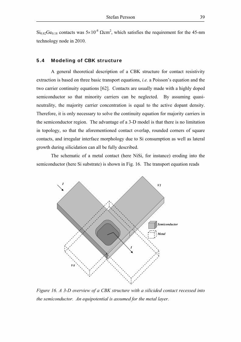
Stefan Persson 39
Si0.82Ge0.18 contacts was 5×10⁻⁸ Ωcm2, which satisfies the requirement for the 45-nm
technology node in 2010.
5.4 Modeling of CBK structure
A general theoretical description of a CBK structure for contact resistivity
extraction is based on three basic transport equations, i.e. a Poisson’s equation and the
two carrier continuity equations [62]. Contacts are usually made with a highly doped
semiconductor so that minority carriers can be neglected. By assuming quasi-
neutrality, the majority carrier concentration is equal to the active dopant density.
Therefore, it is only necessary to solve the continuity equation for majority carriers in
the semiconductor region. The advantage of a 3-D model is that there is no limitation
in topology, so that the aforementioned contact overlap, rounded corners of square
contacts, and irregular interface morphology due to Si consumption as well as lateral
growth during silicidation can all be fully described.
The schematic of a metal contact (here NiSi, for instance) eroding into the
semiconductor (here Si substrate) is shown in Fig. 16. The transport equation reads
V1I
I
V4
Semiconductor
Metal
Figure 16. A 3-D overview of a CBK structure with a silicided contact recessed into
the semiconductor. An equipotential is assumed for the metal layer.
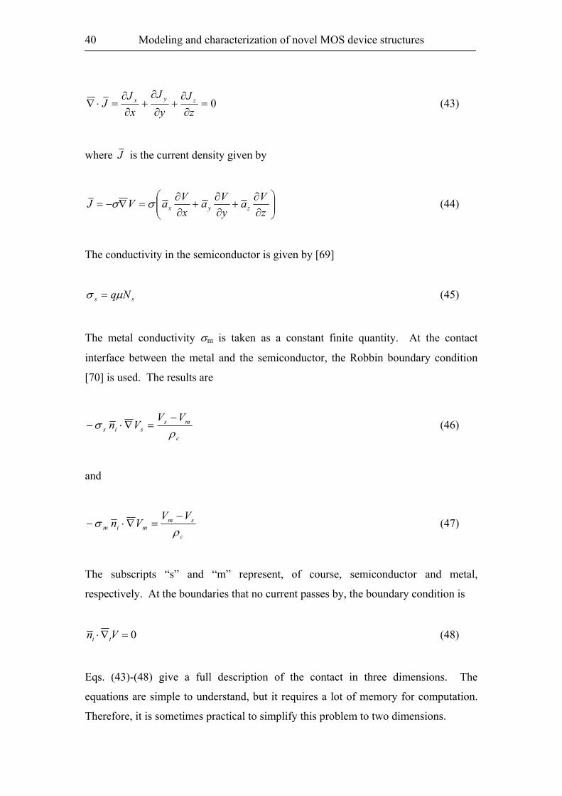
Modeling and characterization of novel MOS device structures
40
0=∂
∂+
∂
∂+
∂∂
=⋅∇z
Jy
Jx
JJ zyx (43)
where J is the current density given by
⎟⎟⎠
⎞⎜⎜⎝
⎛∂∂
+∂∂
+∂∂
=∇−=zVa
yVa
xVaVJ zyxσσ (44)
The conductivity in the semiconductor is given by [69]
ss Nqµσ = (45)
The metal conductivity σm is taken as a constant finite quantity. At the contact
interface between the metal and the semiconductor, the Robbin boundary condition
[70] is used. The results are
c
mssis
VVVn
ρσ
−=∇⋅− (46)
and
c
smmim
VVVn
ρσ
−=∇⋅− (47)
The subscripts “s” and “m” represent, of course, semiconductor and metal,
respectively. At the boundaries that no current passes by, the boundary condition is
0=∇⋅ Vn ti (48)
Eqs. (43)-(48) give a full description of the contact in three dimensions. The
equations are simple to understand, but it requires a lot of memory for computation.
Therefore, it is sometimes practical to simplify this problem to two dimensions.
Stefan Persson 41
Transformation of the 3-D model to a 2-D model is based on a few
simplifications [62]. The first is that the contact interface is regarded as a 2-D surface
perpendicular to the z-axis, as shown in Fig. 17. The semiconductor (diffusion) layer
is located below the contact and its resistivity is independent of x and y spatial
variables. The metal is assumed as a perfect conductor and an equipotential prevails.
The sheet resistance of the semiconductor layer is given by
( )∫=
jz
s
s
dzz
R
0
1
σ
(49)
A new variable, the conductivity weighted average potential, is defined as
( ) ( )∫==jz
ss dzzyxVzRyxVaVa0
,,),( σ (50)
With the first two terms of Eq. (43), Eq. (44) can be written as
V1I
I
-zyx
∫ ∫==A A
Tsc
dALVa
RVadAI 2
11ρ
A
zj
Figure 17. In the 2-D model, the contact is a mathematical plane at the interface
perpendicular to the z-axis.
Modeling and characterization of novel MOS device structures
42
( ) ( ) 0,, =∂∂
+∇⋅∇−zJzyxVz z
tst σ (51)
where t∇ is a 2-D gradient operator, which is normal to the z-axis. It is defined as
ya
xa yxt ∂
∂+
∂∂
≡∇ (52)
By integrating Eq. (51) along the z-axis and using Eq. (49), Eq. (51) becomes
( ) ( ) ( )jzzts
zJJyxVaR
−=∇− 0,1 2 (53)
Since there is no current in the z-direction outside the contact, the following is true:
( ) 0,2 =∇ yxVat (54)
Inside the contact, the current is Jz(0), see Fig. 18. Since the metal resistivity is zero,
( )c
ts
VayxVaR ρ
−=∇−
0,1 2 (55)
or in a more convenient form
( ) 22 ,
Tt L
VayxVa =∇ (56)
where LT has already been defined in Eq. (42). The total current is the integral over
the contact, given by
∫ ∫==A A
Tsc
dALVa
RVadAI 2
11ρ
(57)
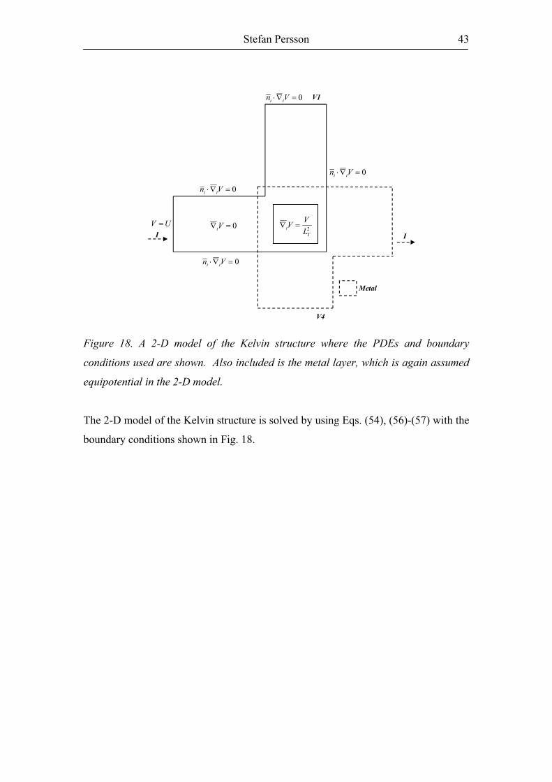
Stefan Persson 43
The 2-D model of the Kelvin structure is solved by using Eqs. (54), (56)-(57) with the
boundary conditions shown in Fig. 18.
0=∇⋅ Vn ti
0=∇⋅ Vn ti
UV =
0=∇⋅ Vn ti
0=∇⋅ Vn ti
2T
t LVV =∇0=∇ Vt
I I
V1
V4
Metal
Figure 18. A 2-D model of the Kelvin structure where the PDEs and boundary
conditions used are shown. Also included is the metal layer, which is again assumed
equipotential in the 2-D model.

Modeling and characterization of novel MOS device structures
44
Stefan Persson 45
6. Summary
This thesis examines the possibility to integrate high-κ gate dielectric,
retrograde Si1-xGex channel and silicided contacts in a conventional, planar MOSFET.
For all the three major areas studied, the thesis attempts to entail a balance between
theoretical evaluations and experimental characterizations.
MOSFETs with Si and strained-Si0.7Ge0.3 surface-channels integrated with
high-κ gate dielectrics and metal gates were manufactured and examined. Three
different gate stacks investigated were TiN/Al2O3, TiN/Al2O3/HfAlOx/Al2O3, and
TiN/Al2O3/HfO2/Al2O3, all deposited by means of ALD. The Si0.7Ge0.3 pMOSFETs
exhibited a more than 30% increase in current drive and peak transconductance
compared to the Si pMOSFET with the same gate stack. The extracted effective
mobility for the Si pMOSFET coincided with the universal mobility curve, indicating
that the high-κ/Si interface was of high quality. The extracted mobility for the
Si1-xGex pMOSFET was however heavily distorted with a slow mobility roll-off at
low vertical electric field. This distortion was explained as a result of trapping of a
considerable fraction of the inversion carriers. A procedure for calculation of the
mobile inversion carriers for correct determination of channel carrier mobility was
presented. The effective mobility curve after compensation for the trapped carriers
still showed a certain degree of distortion most likely due to Coulomb scattering by
the trapped charges or charged traps.
A charge sheet model for MOSFETs with a retrograde channel aiming at
short-channel effect control, threshold voltage control and mobility enhancement was
developed. The emphasis was placed on variations of surface potential, drain current,
intrinsic charge, and intrinsic capacitances with the incorporation of a retrograde
channel. When the retrograde channel was assumed ideally abrupt, closed-form
solutions were found for Si channel devices. An extension of the model to include a
strained Si1-xGex channel was also presented, where the band offset in the valence
band was considered. To begin with, the bulk charge was reduced in a retrograde
channel compared to a uniform channel. For the drain current and intrinsic
capacitance components not related to the bulk terminal, their characteristics were
shifted along the gate voltage axis. For the intrinsic capacitances related to the bulk
terminal, their characteristics were both shifted along the gate voltage axis and
reduced in value. Both current and capacitances were compared with ATLAS
Modeling and characterization of novel MOS device structures
46
simulation with an excellent agreement. Although the model is one-dimensional
developed for long-channel MOSFETs, it should also be applicable for short-channel
devices provided that the short channel effects are perfectly controlled.
In order to study how the Ge content would affect the specific contact
resistivity for Ohmic contacts to heavily doped p-type Si1-xGex, two different types of
TiW/Si1-xGex contacts were characterized corresponding to Si1-xGex surface-channel
and buried channel structures. The contact resistivity was found to decrease by an
order of magnitude with increasing the Ge content from 0 to 30 at. %, which was
mainly due to an increase of the valence band energy of the p+ Si1-xGex. Studying
contacts with metal silicides constitutes a major part of this thesis. The drastic
downscaling has led to technological evolutions including the migration from Ti-
based to Ni-based contact metallization scheme. The traditionally used TiSi2-Si
contacts, with an emphasis on the influence of a Nb interlayer, were first examined.
The specific contact resistivity was found to be almost independent of Nb on n-type
Si. On p-type Si, however, the contact resistivity was found to decrease by 2-4 fold in
the presence of Nb. In order to make an accurate specific contact resistivity extraction
with CBK structures, a precise knowledge of contact area and contact overlap was
needed. It was also important to consider unintentional modifications to the interface
morphology induced by processing, such as over-etching and Si consumption during
silicide formation. A three-dimensional numerical model was then necessary in order
to account for all such effects. The three-dimensional modeling was applied to study
advanced contact metallization involving Ni and Si1-xGex forming a NiSi1-xGex on
heavily doped p-type Si1-xGex. This configuration is particularly attractive for low-
resistivity source/drain in pMOSFETs. A low contact resistivity of 5×10⁻⁸ Ωcm2,
satisfying the resistivity requirement for the 45-nm technology node in 2010, was
obtained for the NiSi0.82Ge0.18/p-type Si0.82Ge0.18 contact.
Stefan Persson 47
7. References
[1] J. E. Lilienfeld, US Patents 1,745,175 (1930, filed October 26, 1926),
1,877,140 (1932, filed December 8, 1928) and 1,900,018 (1933, filed March 28,
1928)
[2] D. Kahng and M. M. Atalla, “Silicon-Silicon dioxide field induced devices,”
Solid-State Device Research Conference, Pittsburgh, June 1960.
[3] G. Moore, “Progress in Digital Integrated Electronics,” IEDM Tech. Digest,
pp. 11-12, 1975.
[4] International Technology Roadmap for Semiconductors (ITRS), 2002,
http://public.itrs.net/
[5] H. Iwai and S. Ohmi, “Silicon integrated circuit technology from past to
future,” Microelectronics Reliability, Vol. 42, pp. 465-491, 2002.
[6] Y. Taur, “CMOS design near the limit of scaling,” IBM J. Res. & Dev. Vol.
46, pp. 213-222, 2002.
[7] H.-S. P. Wong, “Beyond the conventional transistor,” IBM J. Res. & Dev.
Vol. 46, pp. 133-168, 2002.
[8] Y. Tsividis, Operation and Modeling of the MOS Transistor, 2nd ed., Boston:
McGraw-Hill, 1999. p. 162.
[9] Y. Tsividis, Operation and Modeling of the MOS Transistor, 2nd ed., Boston:
McGraw-Hill, 1999. p. 72.
[10] Y. Taur and T. Ning, Fundamentals of Modern VLSI Devices, Cambridge:
Cambridge University Press, Cambridge, 1998, p. 229.
[11] H. Dennard, F. H. Gaensslen, V. L. Rideout, E. Bassous, and A. R. LeBlanc,
“Design of ion implanted MOSFETs with very small physical dimentions,” IEEE J.
Solid-State Circuits, SC-9, p.256, 1974.
[12] Y. Taur and T. Ning, Fundamentals of Modern VLSI Devices, Cambridge:
Cambridge University Press, Cambridge, 1998, p. 171.
[13] G. Baccarani, M. R. Wordeman, and R. H. Dennard, “Generalized scaling
theory and its application to a ¼ micrometer MOSFET design,” IEEE Trans. Electron
Dev., ED-31, p. 452, 1984.
[14] S.-I. Takagi, A. Toriumi, M. Iwase, and H. Tango, ”On the Universality of
Inversion Layer Mobility in Si MOSFET’s: Part I-Effects of Substrate Impurity
Concentration,” IEEE Trans. Electron Dev., Vol. 41, pp. 2357-2362, Dec. 1994.
Modeling and characterization of novel MOS device structures
48
[15] S.-I. Takagi, A. Toriumi, M. Iwase, and H. Tango, ”On the Universality of
Inversion Layer Mobility in Si MOSFET’s: Part II-Effects of Surface Orientation,”
IEEE Trans. Electron Dev., Vol. 41, pp. 2363-2368, Dec. 1994.
[16] S.-L. Lo, D.-A. Buchanan, Y. Taur, and W. Wang, ”Quantum-Mechanical
Modeling of Electron Tunneling Current from the Inversion Layer of Ultra-Thin-
Oxide nMOSFET’s,” IEEE Electron Dev. Lett., Vol. 18, pp. 209-211, 1997.
[17] G. D. Wilk, R. M. Wallace, and J. M. Anthony, “High-κ gate dielectrics:
Current status and materials properties considerations,” J. Appl. Phys., Vol. 89, pp.
5243-5275, 2001.
[18] Y. Tsividis, Operation and Modeling of the MOS Transistor, 2nd ed., Boston:
McGraw-Hill, 1999 pp. 257-269.
[19] Y. Taur and T. Ning, Fundamentals of Modern VLSI Devices, Cambridge:
Cambridge University Press, Cambridge, 1998, p. 35.
[20] Y. Taur and T. Ning, Fundamentals of Modern VLSI Devices, Cambridge:
Cambridge University Press, Cambridge, 1998, p. 131.
[21] Y.-C. Yeo, T.-J. King, and C. Hu, “Metal-dielectric band alignment and its
implications for metal gate complementary metal-oxide-semiconductor technology,”
J. Appl. Phys., Vol. 92, pp. 7266-7271, 2002.
[22] J. Kedzieski, et. al., “Metal-gate FinFET and fully-depleted SOI devices using
total gate silicidation,” International Electron Device Meeting, 2002, pp. 247-250.
[23] Y. Taur and T. Ning, Fundamentals of Modern VLSI Devices, Cambridge:
Cambridge University Press, Cambridge, 1998, pp. 74-78.
[24] D. Frank, Y. Taur, and H.-S. Wong, “Generalized Scale Length for Two-
Dimentional Effects in MOSFET’s,” IEEE Electron Dev. Lett., Vol. 19, pp. 385-387,
1998.
[25] G. C.-F. Yeap, S. Krishnan, and M.-R. Lin, “Fringing-induced barrier
lowering (FIBL) in sub-100nm MOSFETs with high-κ gate dielectrics, ” IEE
Electronics Lett., Vol. 34, pp. 1150-1152.
[26] M. Copel, E. Cartier, E. P. Gusev, S. Guha, N. Bojarczuk, and M. Poppeller,”
Robustness of ultrathin aluminum oxide dielectrics on Si(001)”, Appl. Phys. Lett. 78,
pp. 2670-2672, 2001.
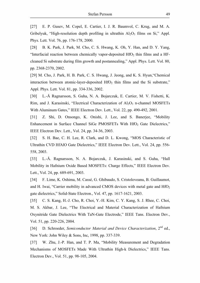
Stefan Persson 49
[27] E. P. Gusev, M. Copel, E. Cartier, I. J. R. Baumvol, C. Krug, and M. A.
Gribelyuk, “High-resolution depth profiling in ultrathin Al2O3 films on Si,” Appl.
Phys. Lett. Vol. 76, pp. 176-178, 2000.
[28] B. K. Park, J. Park, M. Cho, C. S. Hwang, K. Oh, Y. Han, and D. Y. Yang,
“Interfacial reaction between chemically vapor-deposited HfO2 thin films and a HF-
cleaned Si substrate during film growth and postannealing,” Appl. Phys. Lett. Vol. 80,
pp. 2368-2370, 2002.
[29] M. Cho, J. Park, H. B. Park, C. S. Hwang, J. Jeong, and K. S. Hyun,“Chemical
interaction between atomic-layer-deposited HfO2 thin films and the Si substrate,”
Appl. Phys. Lett. Vol. 81, pp. 334-336, 2002.
[30] L.-Å Ragnarsson, S. Guha, N. A. Bojarczuk, E. Cartier, M. V. Fishetti, K.
Rim, and J. Karasinski, “Electrical Characterization of Al2O3 n-channel MOSFETs
With Aluminum Gates,” IEEE Electron Dev. Lett., Vol. 22, pp. 490-492, 2001.
[31] Z. Shi, D. Onsongo, K. Onishi, J. Lee, and S. Banerjee, “Mobility
Enhancement in Surface Channel SiGe PMOSFETs With HfO2 Gate Dielectrics,”
IEEE Electron Dev. Lett., Vol. 24, pp. 34-36, 2003.
[32] S. H. Bae, C. H. Lee, R. Clark, and D. L. Kwong, “MOS Characteristic of
Ultrathin CVD HfAlO Gate Dielectrics,” IEEE Electron Dev. Lett., Vol. 24, pp. 556-
558, 2003.
[33] L.-Å. Ragnarsson, N. A. Bojarczuk, J. Karasinski, and S. Guha, “Hall
Mobility in Hafnium Oxide Based MOSFETs: Charge Effects,” IEEE Electron Dev.
Lett., Vol. 24, pp. 689-691, 2003.
[34] F. Lime, K. Oshima, M. Cassé, G. Ghibaudo, S. Cristoloveanu, B. Guillaumot,
and H. Iwai, “Carrier mobility in advanced CMOS devices with metal gate and HfO2
gate dielectrics,” Solid-State Electron., Vol. 47, pp. 1617-1621, 2003.
[35] C. S. Kang, H.-J. Cho, R. Choi, Y.-H. Kim, C. Y. Kang, S. J. Rhee, C. Choi,
M. S. Akbar, J. Lee, “The Electrical and Material Characterization of Hafnium
Oxynitride Gate Dielectrics With TaN-Gate Electrode,” IEEE Tans. Electron Dev.,
Vol. 51, pp. 220-226, 2004.
[36] D. Schroeder, Semiconductor Material and Device Characterization, 2nd ed.,
New York: John Wiley & Sons, Inc, 1998, pp. 337-339.
[37] W. Zhu, J.-P. Han, and T. P. Ma, “Mobility Measurement and Degradation
Mechanisms of MOSFETs Made With Ultrathin High-k Dielectrics,” IEEE Tans.
Electron Dev., Vol. 51, pp. 98-105, 2004.
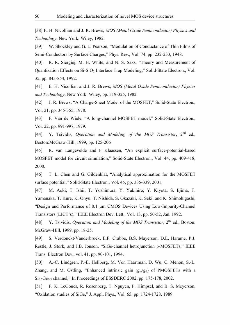
Modeling and characterization of novel MOS device structures
50
[38] E. H. Nicollian and J. R. Brews, MOS (Metal Oxide Semiconductor) Physics and
Technology, New York: Wiley, 1982.
[39] W. Shockley and G. L. Pearson, “Modulation of Conductance of Thin Films of
Semi-Conductors by Surface Charges,” Phys. Rev., Vol. 74, pp. 232-233, 1948.
[40] R. R. Siergiej, M. H. White, and N. S. Saks, “Theory and Measurement of
Quantization Effects on Si-SiO2 Interface Trap Modeling,” Solid-State Electron., Vol.
35, pp. 843-854, 1992.
[41] E. H. Nicollian and J. R. Brews, MOS (Metal Oxide Semiconductor) Physics
and Technology, New York: Wiley, pp. 319-325, 1982.
[42] J. R. Brews, “A Charge-Sheet Model of the MOSFET,” Solid-State Electron.,
Vol. 21, pp. 345-355, 1978.
[43] F. Van de Wiele, “A long-channel MOSFET model,” Solid-State Electron.,
Vol. 22, pp. 991-997, 1979.
[44] Y. Tsividis, Operation and Modeling of the MOS Transistor, 2nd ed.,
Boston:McGraw-Hill, 1999, pp. 125-206
[45] R. van Langevelde and F Klaassen, “An explicit surface-potential-based
MOSFET model for circuit simulation,” Solid-State Electron., Vol. 44, pp. 409-418,
2000.
[46] T. L. Chen and G. Gildenblat, “Analytical approximation for the MOSFET
surface potential,” Solid-State Electron., Vol. 45, pp. 335-339, 2001.
[47] M. Aoki, T. Ishii, T. Yoshimura, Y. Yukihiro, Y. Kiyota, S. Iijima, T.
Yamanaka, T. Kure, K. Ohyu, T. Nishida, S. Okazaki, K. Seki, and K. Shimohigashi,
“Design and Performance of 0.1 µm CMOS Devices Using Low-Impurity-Channel
Transistors (LICT’s),” IEEE Electron Dev. Lett., Vol. 13, pp. 50-52, Jan. 1992.
[48] Y. Tsividis, Operation and Modeling of the MOS Transistor, 2nd ed., Boston:
McGraw-Hill, 1999. pp. 18-25.
[49] S. Verdonckt-Vanderbroek, E.F. Crabbe, B.S. Mayerson, D.L. Harame, P.J.
Restle, J. Stork, and J.B. Jonson, “SiGe-channel hetrojunction p-MOSFETs,” IEEE
Trans. Electron Dev., vol. 41, pp. 90-101, 1994.
[50] A.-C. Lindgren, P.-E. Hellberg, M. Von Haartman, D. Wu, C. Menon, S.-L.
Zhang, and M. Östling, “Enhanced intrinsic gain (gm/gd) of PMOSFETs with a
Si0.7Ge0.3 channel,” In Proceedings of ESSDERC 2002, pp. 175-178, 2002.
[51] F. K. LeGoues, R. Rosenberg, T. Nguyen, F. Himpsel, and B. S. Meyerson,
“Oxidation studies of SiGe,” J. Appl. Phys., Vol. 65, pp. 1724-1728, 1989.
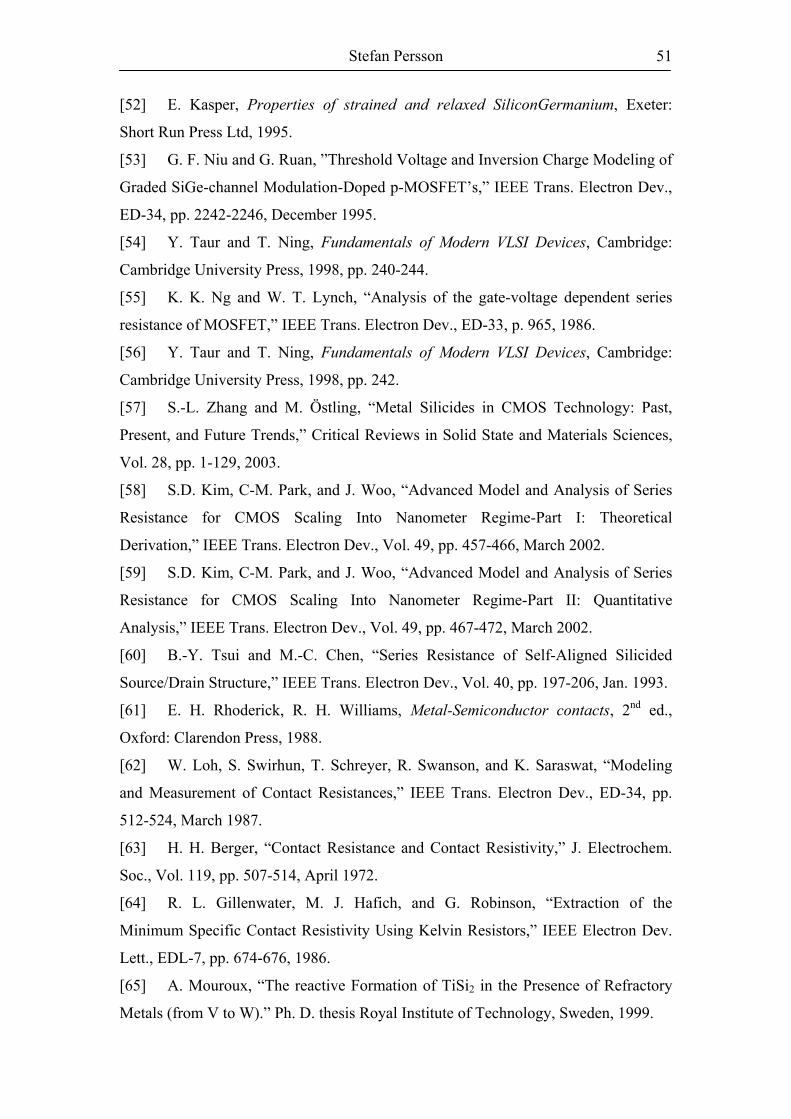
Stefan Persson 51
[52] E. Kasper, Properties of strained and relaxed SiliconGermanium, Exeter:
Short Run Press Ltd, 1995.
[53] G. F. Niu and G. Ruan, ”Threshold Voltage and Inversion Charge Modeling of
Graded SiGe-channel Modulation-Doped p-MOSFET’s,” IEEE Trans. Electron Dev.,
ED-34, pp. 2242-2246, December 1995.
[54] Y. Taur and T. Ning, Fundamentals of Modern VLSI Devices, Cambridge:
Cambridge University Press, 1998, pp. 240-244.
[55] K. K. Ng and W. T. Lynch, “Analysis of the gate-voltage dependent series
resistance of MOSFET,” IEEE Trans. Electron Dev., ED-33, p. 965, 1986.
[56] Y. Taur and T. Ning, Fundamentals of Modern VLSI Devices, Cambridge:
Cambridge University Press, 1998, pp. 242.
[57] S.-L. Zhang and M. Östling, “Metal Silicides in CMOS Technology: Past,
Present, and Future Trends,” Critical Reviews in Solid State and Materials Sciences,
Vol. 28, pp. 1-129, 2003.
[58] S.D. Kim, C-M. Park, and J. Woo, “Advanced Model and Analysis of Series
Resistance for CMOS Scaling Into Nanometer Regime-Part I: Theoretical
Derivation,” IEEE Trans. Electron Dev., Vol. 49, pp. 457-466, March 2002.
[59] S.D. Kim, C-M. Park, and J. Woo, “Advanced Model and Analysis of Series
Resistance for CMOS Scaling Into Nanometer Regime-Part II: Quantitative
Analysis,” IEEE Trans. Electron Dev., Vol. 49, pp. 467-472, March 2002.
[60] B.-Y. Tsui and M.-C. Chen, “Series Resistance of Self-Aligned Silicided
Source/Drain Structure,” IEEE Trans. Electron Dev., Vol. 40, pp. 197-206, Jan. 1993.
[61] E. H. Rhoderick, R. H. Williams, Metal-Semiconductor contacts, 2nd ed.,
Oxford: Clarendon Press, 1988.
[62] W. Loh, S. Swirhun, T. Schreyer, R. Swanson, and K. Saraswat, “Modeling
and Measurement of Contact Resistances,” IEEE Trans. Electron Dev., ED-34, pp.
512-524, March 1987.
[63] H. H. Berger, “Contact Resistance and Contact Resistivity,” J. Electrochem.
Soc., Vol. 119, pp. 507-514, April 1972.
[64] R. L. Gillenwater, M. J. Hafich, and G. Robinson, “Extraction of the
Minimum Specific Contact Resistivity Using Kelvin Resistors,” IEEE Electron Dev.
Lett., EDL-7, pp. 674-676, 1986.
[65] A. Mouroux, “The reactive Formation of TiSi2 in the Presence of Refractory
Metals (from V to W).” Ph. D. thesis Royal Institute of Technology, Sweden, 1999.
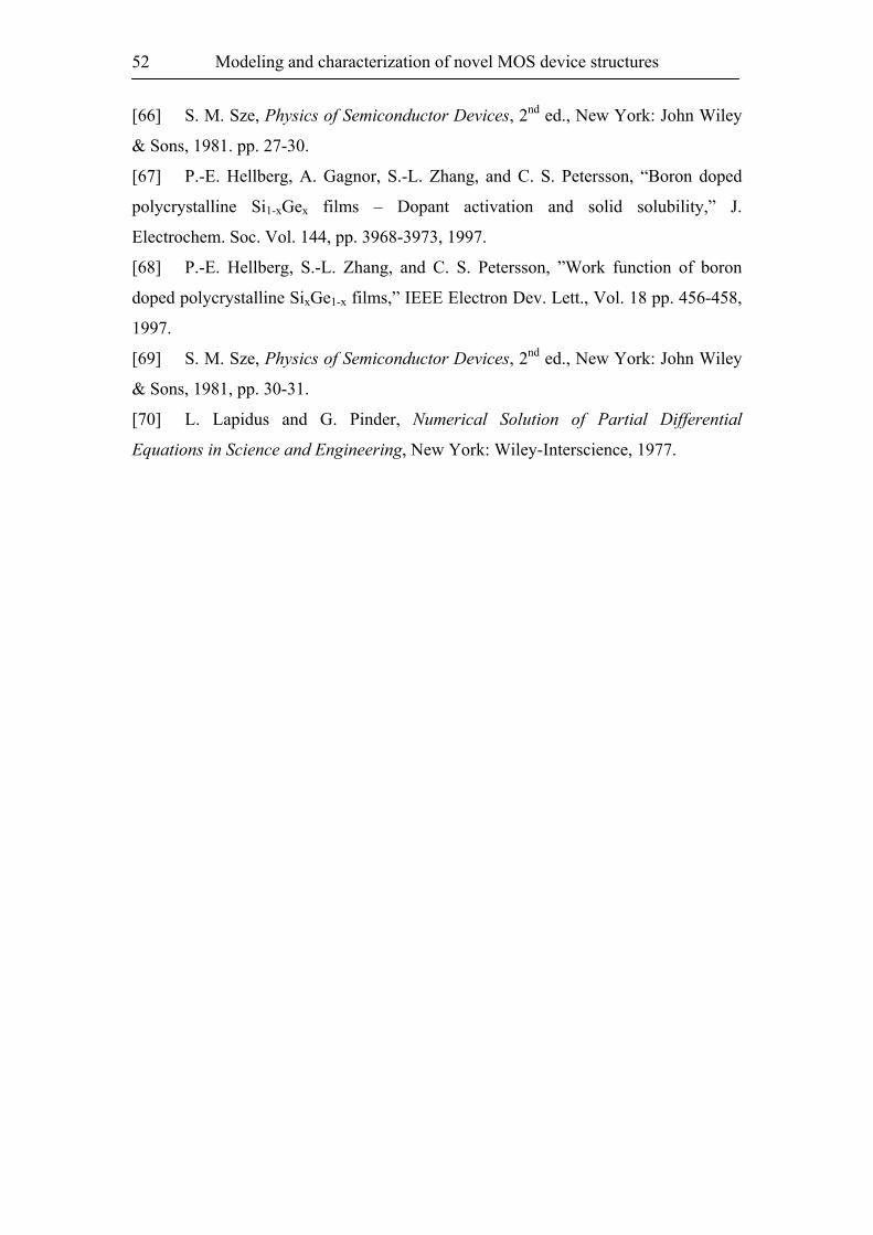
Modeling and characterization of novel MOS device structures
52
[66] S. M. Sze, Physics of Semiconductor Devices, 2nd ed., New York: John Wiley
& Sons, 1981. pp. 27-30.
[67] P.-E. Hellberg, A. Gagnor, S.-L. Zhang, and C. S. Petersson, “Boron doped
polycrystalline Si1-xGex films – Dopant activation and solid solubility,” J.
Electrochem. Soc. Vol. 144, pp. 3968-3973, 1997.
[68] P.-E. Hellberg, S.-L. Zhang, and C. S. Petersson, ”Work function of boron
doped polycrystalline SixGe1-x films,” IEEE Electron Dev. Lett., Vol. 18 pp. 456-458,
1997.
[69] S. M. Sze, Physics of Semiconductor Devices, 2nd ed., New York: John Wiley
& Sons, 1981, pp. 30-31.
[70] L. Lapidus and G. Pinder, Numerical Solution of Partial Differential
Equations in Science and Engineering, New York: Wiley-Interscience, 1977.