Embed Size (px)
DESCRIPTION
Provides great results in the field of chemical vapor deposition.
Citation preview

MOCVD & MBE CEE135
Wen0ng Hou 2013-‐12-‐03
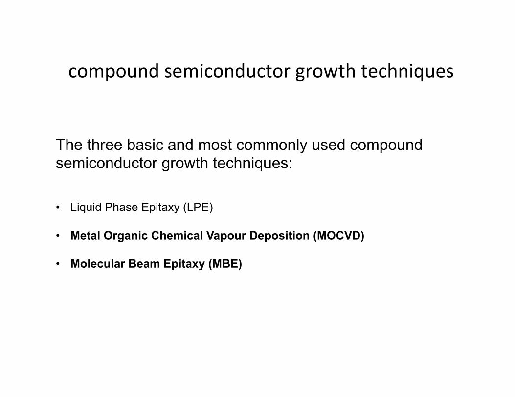
compound semiconductor growth techniques
The three basic and most commonly used compound semiconductor growth techniques: • Liquid Phase Epitaxy (LPE)
• Metal Organic Chemical Vapour Deposition (MOCVD)
• Molecular Beam Epitaxy (MBE)
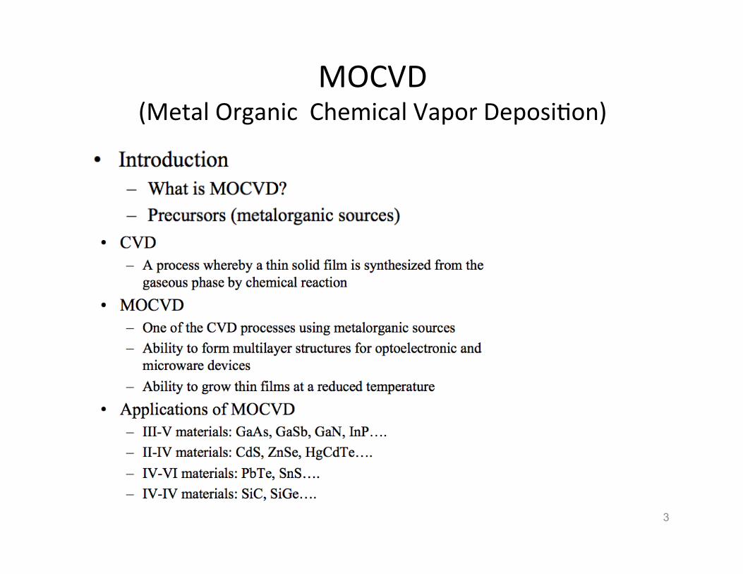
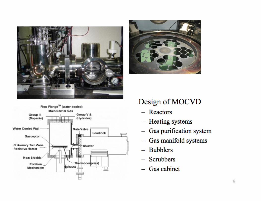
MOCVD (Metal Organic Chemical Vapor Deposi0on)
3
4
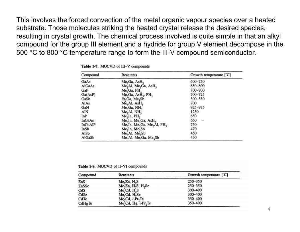
This involves the forced convection of the metal organic vapour species over a heated substrate. Those molecules striking the heated crystal release the desired species, resulting in crystal growth. The chemical process involved is quite simple in that an alkyl compound for the group III element and a hydride for group V element decompose in the 500 °C to 800 °C temperature range to form the III-V compound semiconductor.
5
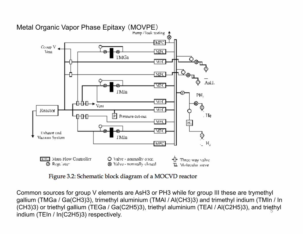
Metal Organic Vapor Phase Epitaxy (MOVPE)
Common sources for group V elements are AsH3 or PH3 while for group III these are trymethyl gallium (TMGa / Ga(CH3)3), trimethyl aluminium (TMAl / Al(CH3)3) and trimethyl indium (TMIn / In(CH3)3) or triethyl gallium (TEGa / Ga(C2H5)3), triethyl aluminium (TEAl / Al(C2H5)3), and triethyl indium (TEIn / In(C2H5)3) respectively.
6
7
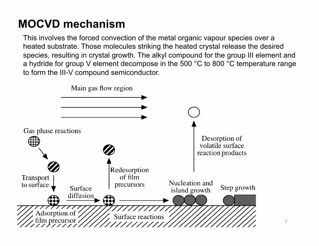
MOCVD mechanism This involves the forced convection of the metal organic vapour species over a heated substrate. Those molecules striking the heated crystal release the desired species, resulting in crystal growth. The alkyl compound for the group III element and a hydride for group V element decompose in the 500 °C to 800 °C temperature range to form the III-V compound semiconductor.

GaN could be grown in a reactor on a substrate by introducing Trimethygallium ((CH3)3Ga) and ammounium (NH3). Formation of the epitaxial layer occurs by final pyrolysis of the constituent chemicals at the substrate surface.
http://en.wikipedia.org/wiki/Metalorganic_vapour_phase_epitaxy
MOCVD Growth of GaN
TMGa molecules deposit and react on surface
NH3 molecules react on surface, leaving N to react and form GaN and CH4
MOCVD: Working condi0ons
9
This takes place not in a vacuum, but from the gas phase at moderate pressures (10 to 760 Torr). As such, this technique is preferred for the formation of devices incorporating thermodynamically metastable alloys, and it has become a major process in the manufacture of optoelectronics.
T too high: desorption, nitrogen vacancies. T too low: impurities incorporation, low surface mobility, structure defects; Usually temperature ~1050 °C

10
• Advantages – Faster growth than MBE, can be a few microns per hour; multi-wafer capability easily achievable – Higher temperature growth; growth process is thermodynamically favorable • Disadvantages – Difficult to monitor growth rate exactly (no Rheed possible due to higher pressure) – Not as abrupt a process as MBE due to gas flow issues and memory effects – Toxic gases are to be handled
Benefits and Drawbacks of MOCVD

Molecular Beam Epitaxy (MBE)
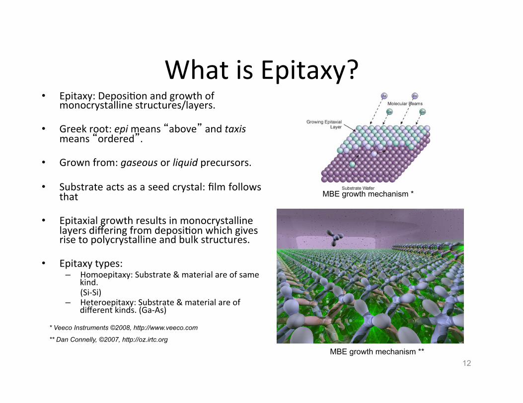
What is Epitaxy? • Epitaxy: Deposi0on and growth of
monocrystalline structures/layers. • Greek root: epi means “above” and taxis
means “ordered”.
• Grown from: gaseous or liquid precursors.
• Substrate acts as a seed crystal: film follows that
• Epitaxial growth results in monocrystalline
layers differing from deposi0on which gives rise to polycrystalline and bulk structures.
• Epitaxy types: – Homoepitaxy: Substrate & material are of same
kind. (Si-‐Si)
– Heteroepitaxy: Substrate & material are of different kinds. (Ga-‐As)
12
* Veeco Instruments ©2008, http://www.veeco.com
** Dan Connelly, ©2007, http://oz.irtc.org
MBE growth mechanism *
MBE growth mechanism **
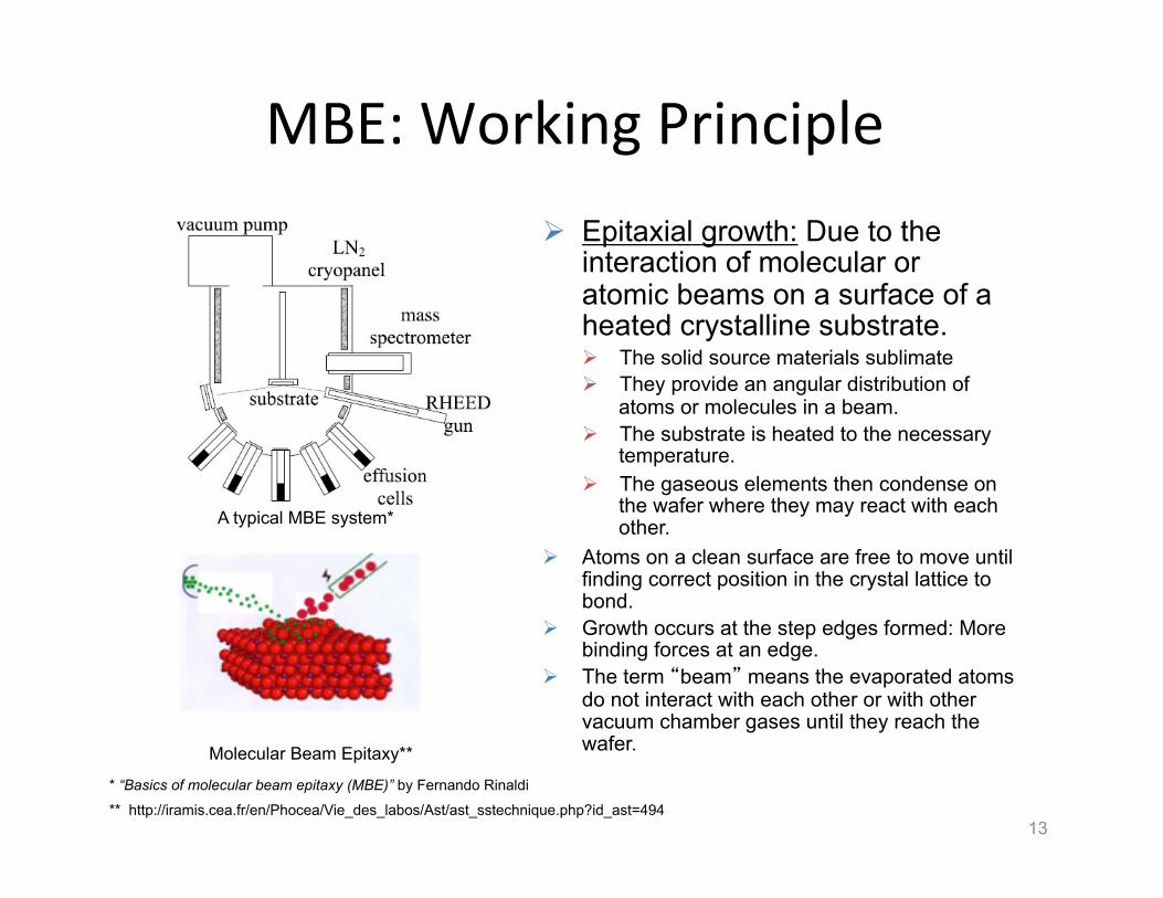
MBE: Working Principle
13
A typical MBE system*
* “Basics of molecular beam epitaxy (MBE)” by Fernando Rinaldi
Ø Epitaxial growth: Due to the interaction of molecular or atomic beams on a surface of a heated crystalline substrate. Ø The solid source materials sublimate Ø They provide an angular distribution of
atoms or molecules in a beam. Ø The substrate is heated to the necessary
temperature. Ø The gaseous elements then condense on
the wafer where they may react with each other.
Molecular Beam Epitaxy**
** http://iramis.cea.fr/en/Phocea/Vie_des_labos/Ast/ast_sstechnique.php?id_ast=494
Ø Atoms on a clean surface are free to move until finding correct position in the crystal lattice to bond.
Ø Growth occurs at the step edges formed: More binding forces at an edge.
Ø The term “beam” means the evaporated atoms do not interact with each other or with other vacuum chamber gases until they reach the wafer.
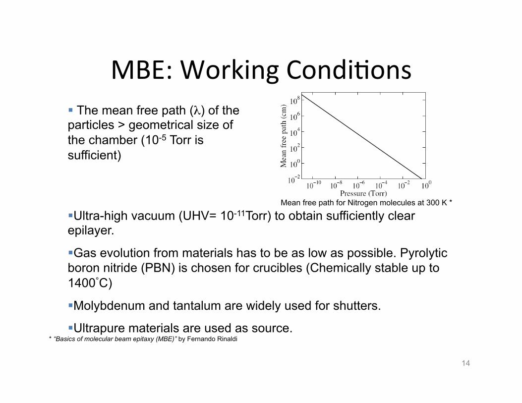
MBE: Working Condi0ons
14
§ The mean free path (λ) of the particles > geometrical size of the chamber (10-5 Torr is sufficient)
§ Ultra-high vacuum (UHV= 10-11Torr) to obtain sufficiently clear epilayer.
§ Gas evolution from materials has to be as low as possible. Pyrolytic boron nitride (PBN) is chosen for crucibles (Chemically stable up to 1400°C)
§ Molybdenum and tantalum are widely used for shutters.
§ Ultrapure materials are used as source.
Mean free path for Nitrogen molecules at 300 K *
* “Basics of molecular beam epitaxy (MBE)” by Fernando Rinaldi
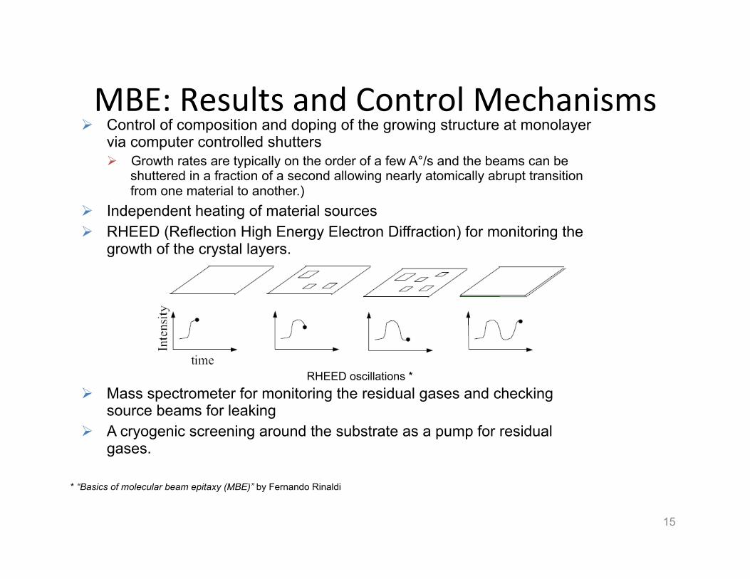
MBE: Results and Control Mechanisms
15
RHEED oscillations *
* “Basics of molecular beam epitaxy (MBE)” by Fernando Rinaldi
Ø Control of composition and doping of the growing structure at monolayer via computer controlled shutters Ø Growth rates are typically on the order of a few A°/s and the beams can be
shuttered in a fraction of a second allowing nearly atomically abrupt transition from one material to another.)
Ø Independent heating of material sources Ø RHEED (Reflection High Energy Electron Diffraction) for monitoring the
growth of the crystal layers.
Ø Mass spectrometer for monitoring the residual gases and checking source beams for leaking
Ø A cryogenic screening around the substrate as a pump for residual gases.
16
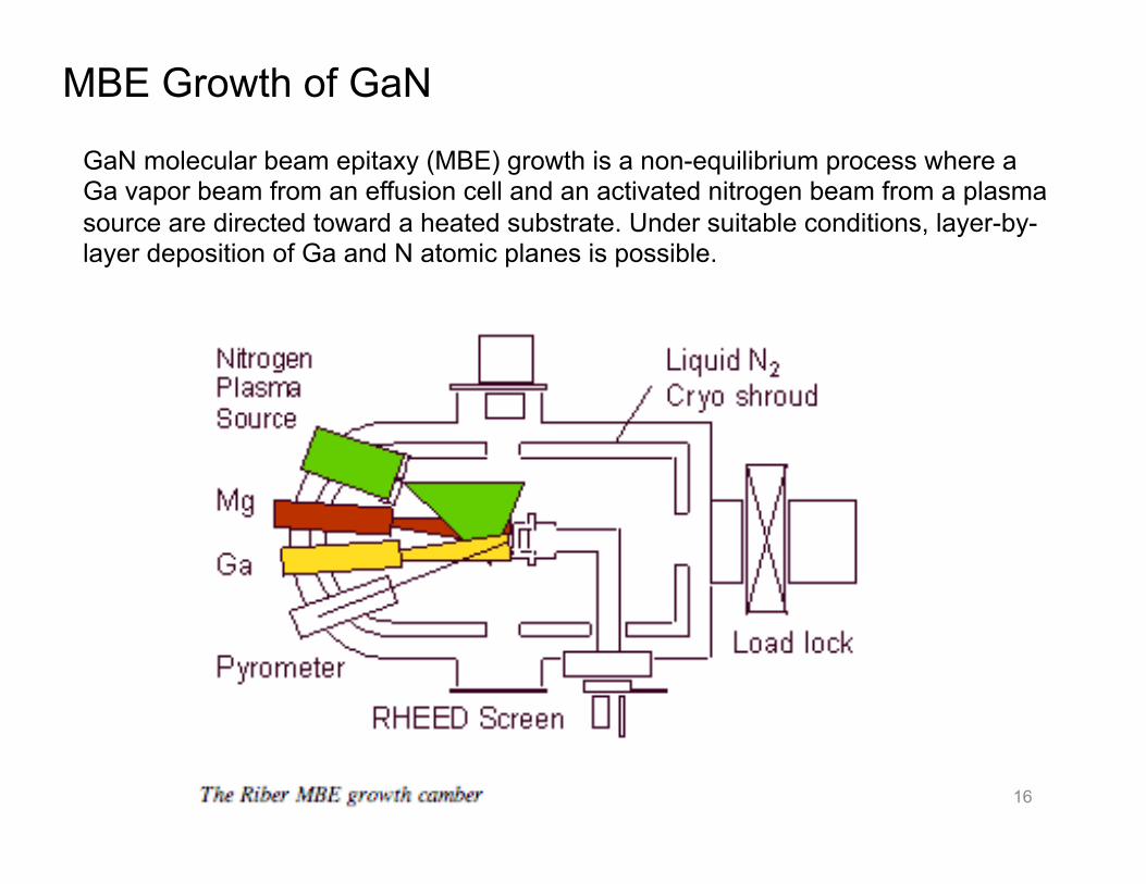
MBE Growth of GaN
GaN molecular beam epitaxy (MBE) growth is a non-equilibrium process where a Ga vapor beam from an effusion cell and an activated nitrogen beam from a plasma source are directed toward a heated substrate. Under suitable conditions, layer-by-layer deposition of Ga and N atomic planes is possible.
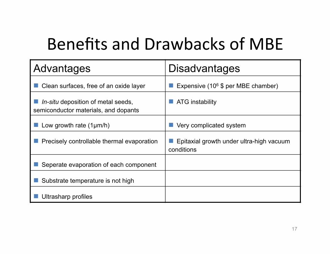
Benefits and Drawbacks of MBE Advantages Disadvantages n Clean surfaces, free of an oxide layer n Expensive (106 $ per MBE chamber)
n In-situ deposition of metal seeds, semiconductor materials, and dopants
n ATG instability
n Low growth rate (1µm/h) n Very complicated system n Precisely controllable thermal evaporation n Epitaxial growth under ultra-high vacuum
conditions
n Seperate evaporation of each component n Substrate temperature is not high n Ultrasharp profiles
17
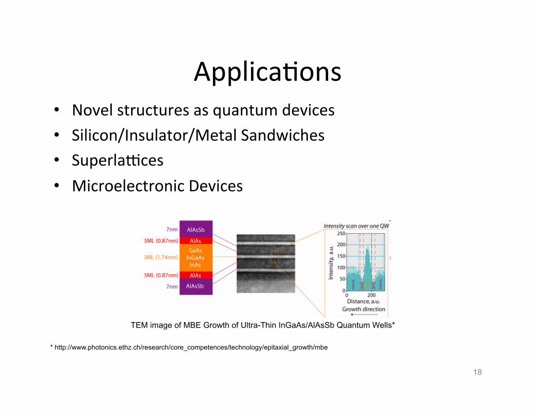
Applica0ons • Novel structures as quantum devices • Silicon/Insulator/Metal Sandwiches • Superla]ces • Microelectronic Devices
18
TEM image of MBE Growth of Ultra-Thin InGaAs/AlAsSb Quantum Wells*
* http://www.photonics.ethz.ch/research/core_competences/technology/epitaxial_growth/mbe
Conclusions of MBE • Typically in ultra-‐high vacuum • Deposi0on rates are very low (1monolayer/second) • Very well controlled (Shu^ering: 0.1s) • Grow films with good crystal structure • O_en use mul0ple sources to grow alloy films • Deposi0on rate is so low that substrate temperature
doesn’t need to be as high • Expensive • Sophis0cated system
19

MBE vs. MOCVD
20


![GRAfox Highlightgrafox.pdi-berlin.de/highlights/d_G_H_Faceting.pdf · for MBE[7,8] and MOCVD[12], while all other orientations resulted in faceted or macroscopically rough surfaces.[13,14,15,5]](https://img.dokumen.tips/doc/110x75/5e8806eac322fa791e09ff06/grafox-for-mbe78-and-mocvd12-while-all-other-orientations-resulted-in-faceted.jpg)