Embed Size (px)
Citation preview
Mobile Intel Pentium 4 Processor-MDatasheet
June 2003
Order Number: 250686-007

2 Mobile Intel Pentium 4 Processor-M Datasheet
Information in this document is provided solely to enable use of Intel products. Intel assumes no liability whatsoever, including infringement of any patent or copyright, for sale and use of Intel products except as provided in Intel's Terms and Conditions of Sale for such products. Information contained herein supersedes previously published specifications on these devices from Intel.
Actual system-level properties, such as skin temperature, are a function of various factors, including component placement, component power characteristics, system power and thermal management techniques, software application usage and general system design. Intel is not responsible for its customers' system designs, nor is Intel responsible for ensuring that its customers' products comply with all applicable laws and regulations. Intel provides this and other thermal design information for informational purposes only. System design is the sole responsibility of Intel's customers, and Intel's customers should not rely on any Intel-provided information as either an endorsement or recommendation of any particular system design characteristics.
Information in this document is provided in connection with Intel products. No license, express or implied, by estoppel or otherwise, to any intellectual property rights is granted by this document. Except as provided in Intel’s Terms and Conditions of Sale for such products, Intel assumes no liability whatsoever, and Intel disclaims any express or implied warranty, relating to sale and/or use of Intel products including liability or warranties relating to fitness for a particular purpose, merchantability, or infringement of any patent, copyright or other intellectual property right. Intel products are not intended for use in medical, life saving, or life sustaining applications.
Intel may make changes to specifications and product descriptions at any time, without notice.
Designers must not rely on the absence or characteristics of any features or instructions marked “reserved” or “undefined.” Intel reserves these for future definition and shall have no responsibility whatsoever for conflicts or incompatibilities arising from future changes to them.
The Mobile Intel Pentium 4 Processor-M may contain design defects or errors known as errata which may cause the product to deviate from published specifications. Current characterized errata are available on request.
Contact your local Intel sales office or your distributor to obtain the latest specifications and before placing your product order.
Copies of documents which have an ordering number and are referenced in this document, or other Intel literature, may be obtained by calling 1-800-548-4725 or by visiting Intel’s Website at http://www.intel.com
Copyright © Intel Corporation 2000-2003.
Intel, Pentium, Intel NetBurst, and SpeedStep are registered trademarks or trademarks of Intel Corporation and its subsidiaries in the United States and other countries.
* Other brands and names are the property of their respective owners.

Contents1. Introduction.........................................................................................................................9
1.1 Terminology.........................................................................................................111.2 References ..........................................................................................................11
2. Electrical Specifications....................................................................................................132.1 System Bus and GTLREF...................................................................................132.2 Power and Ground Pins ......................................................................................132.3 Decoupling Guidelines ........................................................................................13
2.3.1 VCC Decoupling .....................................................................................142.3.2 System Bus AGTL+ Decoupling.............................................................142.3.3 System Bus Clock (BCLK[1:0]) and Processor Clocking .......................14
2.4 Voltage Identification and Power Sequencing.....................................................152.4.1 Enhanced Intel® SpeedStep® Technology............................................162.4.2 Phase Lock Loop (PLL) Power and Filter...............................................172.4.3 Catastrophic Thermal Protection............................................................18
2.5 Signal Terminations, Unused Pins and TESTHI[10:0] ........................................182.6 System Bus Signal Groups .................................................................................202.7 Asynchronous GTL+ Signals...............................................................................222.8 Test Access Port (TAP) Connection....................................................................222.9 System Bus Frequency Select Signals (BSEL[1:0])............................................222.10 Maximum Ratings................................................................................................232.11 Processor DC Specifications...............................................................................232.12 AGTL+ System Bus Specifications .....................................................................342.13 System Bus AC Specifications ............................................................................352.14 Processor AC Timing Waveforms .......................................................................40
3. System Bus Signal Quality Specifications........................................................................513.1 System Bus Clock (BCLK) Signal Quality Specifications and Measurement
Guidelines ...........................................................................................................513.2 System Bus Signal Quality Specifications and Measurement Guidelines...........523.3 System Bus Signal Quality Specifications and Measurement Guidelines...........55
3.3.1 Overshoot/Undershoot Guidelines .........................................................553.3.2 Overshoot/Undershoot Magnitude .........................................................553.3.3 Overshoot/Undershoot Pulse Duration...................................................553.3.4 Activity Factor.........................................................................................563.3.5 Reading Overshoot/Undershoot Specification Tables............................563.3.6 Conformance Determination to Overshoot/Undershoot Specifications ..57
4. Package Mechanical Specifications .................................................................................614.1 Processor Pin-Out ...............................................................................................64
5. Pin Listing and Signal Definitions .....................................................................................675.1 Mobile Intel Pentium 4 Processor-M Pin Assignments........................................675.2 Alphabetical Signals Reference ..........................................................................81
6. Thermal Specifications and Design Considerations.........................................................896.1 Thermal Specifications ........................................................................................90
Mobile Intel Pentium 4 Processor-M Datasheet 3

Mobile Intel Pentium 4 Processor-M
6.1.1 Thermal Diode........................................................................................ 906.1.2 Thermal Monitor ..................................................................................... 91
7. Configuration and Low Power Features........................................................................... 937.1 Power-On Configuration Options ........................................................................ 937.2 Clock Control and Low Power States.................................................................. 93
7.2.1 Normal State .......................................................................................... 937.2.2 AutoHALT Powerdown State ................................................................. 937.2.3 Stop-Grant State .................................................................................... 947.2.4 HALT/Grant Snoop State ....................................................................... 957.2.5 Sleep State............................................................................................. 957.2.6 Deep Sleep State ................................................................................... 957.2.7 Deeper Sleep State ................................................................................ 96
7.3 Enhanced Intel SpeedStep Technology.............................................................. 96
8. Debug Tools Specifications..............................................................................................978.1 Logic Analyzer Interface (LAI) ............................................................................ 97
8.1.1 Mechanical Considerations .................................................................... 978.1.2 Electrical Considerations........................................................................ 97
4 Mobile Intel Pentium 4 Processor-M Datasheet

Figures1 VCCVID Pin Voltage and Current Requirements ................................................152 Typical VCCIOPLL, VCCA and VSSA Power Distribution ..................................173 Phase Lock Loop (PLL) Filter Requirements .....................................................184 Illustration of VCC Static and Transient Tolerances (VID = 1.30 V)....................265 Illustration of VCC Static and Transient Tolerances (VID = 1.20 V)....................286 Illustration of Deep Sleep VCC Static and Transient Tolerances (VID
Setting = 1.30 V) .................................................................................................297 ITPCLKOUT[1:0] Output Buffer Diagram ............................................................348 AC Test Circuit ....................................................................................................419 TCK Clock Waveform..........................................................................................4110 Differential Clock Waveform................................................................................4211 Differential Clock Crosspoint Specification..........................................................4312 System Bus Common Clock Valid Delay Timings...............................................4313 System Bus Reset and Configuration Timings....................................................4414 Source Synchronous 2X (Address) Timings .......................................................4415 Source Synchronous 4X Timings ........................................................................4516 Power Up Sequence ...........................................................................................4617 Power Down Sequence.......................................................................................4618 Test Reset Timings .............................................................................................4719 THERMTRIP# to Vcc Timing...............................................................................4720 FERR#/PBE# Valid Delay Timing .......................................................................4721 TAP Valid Delay Timing ......................................................................................4822 ITPCLKOUT Valid Delay Timing .........................................................................4823 Stop Grant/Sleep/Deep Sleep Timing .................................................................4924 Enhanced Intel SpeedStep Technology/Deep Sleep Timing ..............................5025 BCLK Signal Integrity Waveform.........................................................................5226 Low-to-High System Bus Receiver Ringback Tolerance.....................................5327 High-to-Low System Bus Receiver Ringback Tolerance.....................................5328 Low-to-High System Bus Receiver Ringback Tolerance for PWRGOOD and TAP
Buffers .................................................................................................................5429 High-to-Low System Bus Receiver Ringback Tolerance for PWRGOOD and TAP
Buffers .................................................................................................................5430 Maximum Acceptable Overshoot/Undershoot Waveform ...................................5931 Micro-FCPGA Package Top and Bottom Isometric Views ..................................6132 Micro-FCPGA Package Top and Side View........................................................6233 Micro-FCPGA Package - Bottom View................................................................6434 The Coordinates of the Processor Pins as Viewed From the Top of the
Package. .............................................................................................................6535 Clock Control States............................................................................................94
Mobile Intel Pentium 4 Processor-M Datasheet 5

Mobile Intel Pentium 4 Processor-M
Tables1 References.......................................................................................................... 112 Core Frequency to System Bus Multipliers ......................................................... 143 Voltage Identification Definition........................................................................... 164 System Bus Pin Groups ...................................................................................... 215 BSEL[1:0] Frequency Table for BCLK[1:0] ......................................................... 226 Processor DC Absolute Maximum Ratings ......................................................... 237 Voltage and Current Specifications..................................................................... 248 IMVP-III Voltage Regulator Tolerances for VID = 1.30 V Operating Mode
(Maximum Performance Mode)........................................................................... 259 IMVP-III Voltage Regulator Tolerances for VID = 1.20 V Operating Mode
(Battery Optimized Mode) ................................................................................... 2710 IMVP-III Deep Sleep State Voltage Regulator Tolerances for Maximum
Performance Mode (VID = 1.30 V, VID Offset = 4.62%)..................................... 2811 IMVP-III Deep Sleep State Voltage Regulator Tolerances for Battery Optimized
Mode (VID = 1.20 V, VID Offset = 4.62%) .......................................................... 2912 System Bus Differential BCLK Specifications ..................................................... 3013 AGTL+ Signal Group DC Specifications ............................................................. 3114 Asynchronous GTL+ Signal Group DC Specifications ........................................ 3215 PWRGOOD and TAP Signal Group DC Specifications ...................................... 3316 ITPCLKOUT[1:0] DC Specifications.................................................................... 3317 BSEL [1:0] and VID[4:0] DC Specifications......................................................... 3418 AGTL+ Bus Voltage Definitions........................................................................... 3519 System Bus Differential Clock Specifications...................................................... 3620 System Bus Common Clock AC Specifications .................................................. 3621 System Bus Source Synch AC Specifications AGTL+ Signal Group .................. 3722 Miscellaneous Signals AC Specifications ........................................................... 3823 System Bus AC Specifications (Reset Conditions) ............................................. 3824 TAP Signals AC Specifications ........................................................................... 3925 ITPCLKOUT[1:0] AC Specifications.................................................................... 3926 Stop Grant/Sleep/Deep Sleep/Enhanced Intel SpeedStep Technology AC
Specifications ...................................................................................................... 4027 BCLK Signal Quality Specifications .................................................................... 5128 Ringback Specifications for AGTL+ and Asynchronous GTL+ Signal Groups.... 5229 Ringback Specifications for PWRGOOD Input and TAP Signal Groups............. 5330 Source Synchronous (400 MHz) AGTL+ Signal Group Overshoot/Undershoot
Tolerance ............................................................................................................ 5731 Source Synchronous (200 MHz) AGTL+ Signal Group Overshoot/Undershoot
Tolerance ............................................................................................................ 5832 Common Clock (100 MHz) AGTL+ Signal Group Overshoot/Undershoot
Tolerance ............................................................................................................ 5833 Asynchronous GTL+, PWRGOOD Input, and TAP Signal Groups
Overshoot/Undershoot Tolerance ....................................................................... 5934 Micro-FCPGA Package Dimensions ................................................................... 6335 Pin Listing by Pin Name ...................................................................................... 6836 Pin Listing by Pin Number................................................................................... 7437 Signal Description ............................................................................................... 8138 Power Specifications for the Mobile Intel Pentium 4 Processor-M...................... 8939 Thermal Diode Interface...................................................................................... 90
6 Mobile Intel Pentium 4 Processor-M Datasheet

40 Thermal Diode Specifications..............................................................................9041 Power-On Configuration Option Pins ..................................................................93
Mobile Intel Pentium 4 Processor-M Datasheet 7

Mobile Intel Pentium 4 Processor-M
Revision History
Date Revision Description
March 2002 001 Initial release of the Datasheet
April 2002 002 Updates include:• Added new processor speeds: 1.4 GHz, 1.5 GHz, & 1.8 GHz• Added PROCHOT# signal in Table 21• Updated signal description for PROCHOT# in Table 37 and Section 6.1.2• Updated the description of the Enhanced Intel Speedstep Technology in
sections 2.4.1 and 7.3• Updated PWRGOOD signal in Table 3, Section 2.7, Table 14, Table 21,
Table 28, Table 35, Figure 28, and FIgure 29
June 2002 003 Updates include:• Added specifications for new processor speeds: 1.90 GHz and 2 GHz• Added die length and die width for processors based on B0-step shrink
process in Table 33
September 2002 004 Updates include:• Added 2.2 GHz Mobile Intel Pentium 4 Processor-M specifications.• Current and power specifications updated in Table 7 & Table 38.• Corrected STPCLK#/SLP# timing relationship in Section 7.2.3 to match
parameter T75.
January 2003 005 Updates include:• Added 2.4 GHz Mobile Intel Pentium 4 Processor-M specifications.• Current and power specifications updated in Table 7 & Table 38.• Clarified DBI[3:0]# and THERMTRIP# descriptions in Table 37.• Clarified thermal solution requirements in Section 6.
April 2003 006 Updates include:• Added 2.5 GHz Mobile Intel Pentium 4 Processor-M specifications.• Current and power specifications updated in Table 7 & Table 38.
June 2003 007 Updates include:• Added 2.6 GHz Mobile Intel Pentium 4 Processor-M specifications.• Updated note 5 in Table 22.• Updated THERMTRIP# description in Table 37.
8 Mobile Intel Pentium 4 Processor-M Datasheet

Introduction
1. Introduction
The Mobile Intel Pentium 4 Processor-M is the first Intel mobile processor with the Intel NetBurstTM micro-architecture. The Mobile Intel Pentium 4 Processor-M utilizes a 478-pin, Micro Flip-Chip Pin Grid Array (Micro-FCPGA) package, and plugs into a surface-mount, Zero Insertion Force (ZIF) socket. The Mobile Intel Pentium 4 Processor-M maintains full compatibility with IA-32 software. In this document the Mobile Intel Pentium 4 Processor-M will be referred to as the “Mobile Intel Pentium 4 Processor-M” or simply “the processor.”
The Intel NetBurst micro-architecture features include hyper-pipelined technology, a rapid execution engine, a 400-MHz system bus, and an execution trace cache. The hyper pipelined technology doubles the pipeline depth in the Mobile Intel Pentium 4 Processor-M allowing the processor to reach much higher core frequencies. The rapid execution engine allows the two integer ALUs in the processor to run at twice the core frequency, which allows many integer instructions to execute in 1/2 clock tick. The 400-MHz system bus is a quad-pumped bus running off a 100-MHz system clock making 3.2 GB/sec data transfer rates possible. The execution trace cache is a first level cache that stores approximately 12-k decoded micro-operations, which removes the instruction decoding logic from the main execution path, thereby increasing performance.
Additional features within the Intel NetBurst micro-architecture include advanced dynamic execution, advanced transfer cache, enhanced floating point and multi-media unit, and Streaming SIMD Extensions 2 (SSE2). The advanced dynamic execution improves speculative execution and branch prediction internal to the processor. The advanced transfer cache is a 512 kB, on-die level 2 (L2) cache. A new floating point and multi media unit has been implemented which provides superior performance for multi-media and mathematically intensive applications. Finally, SSE2 adds 144 new instructions for double-precision floating point, SIMD integer, and memory management. Power management capabilities such as AutoHALT, Stop-Grant, Sleep, Deep Sleep, and Deeper Sleep have been incorporated. The processor includes an address bus powerdown capability which removes power from the address and data pins when the system bus is not in use. This feature is always enabled on the processor.
The Streaming SIMD Extensions 2 (SSE2) enable break-through levels of performance in multimedia applications including 3-D graphics, video decoding/encoding, and speech recognition. The new packed double-precision floating-point instructions enhance performance for applications that require greater range and precision, including scientific and engineering applications and advanced 3-D geometry techniques, such as ray tracing.
The Mobile Intel Pentium 4 Processor-M’s 400-MHz Intel NetBurst micro-architecture system bus utilizes a split-transaction, deferred reply protocol like the Intel Pentium 4 Processor. This system bus is not compatible with the P6 processor family bus. The 400-MHz Intel NetBurst micro-architecture system bus uses Source-Synchronous Transfer (SST) of address and data to improve performance by transferring data four times per bus clock (4X data transfer rate, as in AGP 4X). Along with the 4X data bus, the address bus can deliver addresses two times per bus clock and is referred to as a “double-clocked” or 2X address bus. Working together, the 4X data bus and 2X address bus provide a data bus bandwidth of up to 3.2 Gbytes/second.
The processor, when used in conjunction with the requisite Intel SpeedStep technology applet or its equivalent, supports Enhanced Intel SpeedStep technology, which enables real-time dynamic switching of the voltage and frequency between two performance modes. This occurs by switching the bus ratios, core operating voltage, and core processor speeds without resetting the system.
Mobile Intel Pentium 4 Processor-M Datasheet 9

Introduction
The processor system bus uses a variant of GTL+ signalling technology called Assisted Gunning Transceiver Logic (AGTL+) signal technology. The Mobile Intel Pentium 4 Processor-M is available at the following core frequencies:
• 2.6 GHz (in Maximum Performance Mode at 1.30 V). This processor runs at 1.2 GHz (in Battery Optimized Mode at 1.20 V)
• 2.5 GHz (in Maximum Performance Mode at 1.30 V). This processor runs at 1.2 GHz (in Battery Optimized Mode at 1.20 V)
• 2.4 GHz (in Maximum Performance Mode at 1.30 V). This processor runs at 1.2 GHz (in Battery Optimized Mode at 1.20 V)
• 2.2 GHz (in Maximum Performance Mode at 1.30 V). This processor runs at 1.2 GHz (in Battery Optimized Mode at 1.20 V)
• 2.0 GHz (in Maximum Performance Mode at 1.30 V). This processor runs at 1.2 GHz (in Battery Optimized Mode at 1.20 V)
• 1.9 GHz (in Maximum Performance Mode at 1.30 V). This processor runs at 1.2 GHz (in Battery Optimized Mode at 1.20 V)
• 1.8 GHz (in Maximum Performance Mode at 1.30 V). This processor runs at 1.2 GHz (in Battery Optimized Mode at 1.20 V)
• 1.7 GHz (in Maximum Performance Mode at 1.30 V). This processor runs at 1.2 GHz (in Battery Optimized Mode at 1.20 V)
• 1.6 GHz (in Maximum Performance Mode at 1.30 V). This processor runs at 1.2 GHz (in Battery Optimized Mode at 1.20 V)
• 1.5 GHz (in Maximum Performance Mode at 1.30 V). This processor runs at 1.2 GHz (in Battery Optimized Mode at 1.20 V)
• 1.4 GHz (in Maximum Performance Mode at 1.30 V). This processor runs at 1.2 GHz (in Battery Optimized Mode at 1.20 V)
10 Mobile Intel Pentium 4 Processor-M Datasheet

Introduction
1.1 Terminology
A “#” symbol after a signal name refers to an active low signal, indicating a signal is in the active state when driven to a low level. For example, when RESET# is low, a reset has been requested. Conversely, when NMI is high, a nonmaskable interrupt has occurred. In the case of signals where the name does not imply an active state but describes part of a binary sequence (such as address or data), the “#” symbol implies that the signal is inverted. For example, D[3:0] = “HLHL” refers to a hex ‘A’, and D[3:0]# = “LHLH” also refers to a hex “A” (H= High logic level, L= Low logic level).
“System Bus” refers to the interface between the processor and system core logic (a.k.a. the chipset components). The system bus is a multiprocessing interface to processors, memory, and I/O.
Commonly used terms are explained here for clarification:
• Processor — For this document, the term processor shall mean the Mobile Intel Pentium 4 Processor-M in the 478-pin package.
• Keep out zone — The area on or near the processor that system design can not utilize.
• Intel 845MP/845MZ chipsets — Mobile chipsets that will support the Mobile Intel Pentium 4 Processor-M.
• Processor core — Mobile Intel Pentium 4 Processor-M core die with integrated L2 cache.
• Micro-FCPGA package — Micro Flip-Chip Pin Grid Array package with 50-mil pin pitch.
1.2 References
Material and concepts available in the following documents may be beneficial when reading this document.
Table 1. References
Document Order Number
Mobile Intel Pentium 4 Processor-M and Intel 845MP/845MZ Chipset Platform Design Guide 250688-002
Intel Architecture Software Developer's Manual
Volume I: Basic Architecture 245470
Volume II: Instruction Set Reference 245471
Volume III: System Programming Guide 245472
Mobile Intel Pentium 4 Processor-M Datasheet 11

Introduction
This page intentionally left blank.
12 Mobile Intel Pentium 4 Processor-M Datasheet

Electrical Specifications
2. Electrical Specifications
2.1 System Bus and GTLREF
Most Mobile Intel Pentium 4 Processor-M system bus signals use Assisted Gunning Transceiver Logic (AGTL+) signalling technology. As with the Intel P6 family of microprocessors, this signalling technology provides improved noise margins and reduced ringing through low-voltage swings and controlled edge rates. The termination voltage level for the Mobile Intel Pentium 4 Processor-M AGTL+ signals is VCC, which is the operating voltage of the processor core. Previous generations of Intel mobile processors utilize a fixed termination voltage known as VCCT. The use of a termination voltage that is determined by the processor core allows better voltage scaling on the system bus for Mobile Intel Pentium 4 Processor-M. Because of the speed improvements to data and address bus, signal integrity and platform design methods have become more critical than with previous processor families. Design guidelines for the Mobile Intel Pentium 4 Processor-M system bus will be detailed in the Mobile Intel Pentium 4 Processor-M and Intel 845MP/845MZ Chipset Platform Design Guide.
The AGTL+ inputs require a reference voltage (GTLREF) which is used by the receivers to determine if a signal is a logical 0 or a logical 1. GTLREF must be generated on the system board.
Termination resistors are provided on the processor silicon and are terminated to its core voltage (VCC). Intel’s 845MP/845MZ chipsets will also provide on-die termination, thus eliminating the need to terminate the bus on the system board for most AGTL+ signals. However, some AGTL+ signals do not include on-die termination and must be terminated on the system board. For more information, refer to the Mobile Intel Pentium 4 Processor-M and Intel 845MP/845MZ Chipset Platform Design Guide.
The AGTL+ bus depends on incident wave switching. Therefore, timing calculations for AGTL+ signals are based on flight time as opposed to capacitive deratings. Analog signal simulation of the system bus, including trace lengths, is highly recommended when designing a system.
2.2 Power and Ground Pins
For clean on-chip power distribution, the Mobile Intel Pentium 4 Processor-M have 85 VCC (power) and 181 VSS (ground) inputs. All power pins must be connected to VCC, while all VSS pins must be connected to a system ground plane.The processor VCC pins must be supplied with the voltage determined by the VID (Voltage ID) pins and the loadline specifications (see Figure 4 to Figure 6).
2.3 Decoupling Guidelines
Due to its large number of transistors and high internal clock speeds, the processor is capable of generating large average current swings between low and full power states. This may cause voltages on power planes to sag below their minimum values if bulk decoupling is not adequate. Care must be taken in the board design to ensure that the voltage provided to the processor remains within the specifications listed in Table 7. Failure to do so can result in timing violations and/or
Mobile Intel Pentium 4 Processor-M Datasheet 13

Electrical Specifications
affect the long term reliability of the processor. For further information and design guidelines, refer to the Mobile Intel Pentium 4 Processor-M and Intel 845MP/845MZ Chipset Platform Design Guide.
2.3.1 VCC Decoupling
Regulator solutions need to provide bulk capacitance with a low Effective Series Resistance (ESR) and keep a low interconnect resistance from the regulator to the socket. Bulk decoupling for the large current swings when the part is powering on, or entering/exiting low-power states, must be provided by the voltage regulator solution. For more details on decoupling recommendations, please refer to the Mobile Intel Pentium 4 Processor-M and Intel 845MP/845MZ Chipset Platform Design Guide.
2.3.2 System Bus AGTL+ Decoupling
The Mobile Intel Pentium 4 Processor-M integrates signal termination on the die and incorporates high frequency decoupling capacitance on the processor package. Decoupling must also be provided by the system motherboard for proper AGTL+ bus operation. For more information, refer to the Mobile Intel Pentium 4 Processor-M and Intel 845MP/845MZ Chipset Platform Design Guide.
2.3.3 System Bus Clock (BCLK[1:0]) and Processor Clocking
BCLK[1:0] directly controls the system bus interface speed as well as the core frequency of the processor. As in previous generation processors, the Mobile Intel Pentium 4 Processor-M core frequency is a multiple of the BCLK[1:0] frequency. Refer to Table 2 for the Mobile Intel Pentium 4 Processor-M supported ratios.
NOTES:1. Ratio is used for debug purposes only.
Table 2. Core Frequency to System Bus Multipliers
Core Frequency Multiplication of System Core Frequency to System Bus Frequency Notes2
800 MHz 1/8 1
1.2 GHz 1/12
1.4 GHz 1/14
1.5 GHz 1/15
1.6 GHz 1/16
1.7 GHz 1/17
1.8 GHz 1/18
1.9 GHz 1/19
2.0 GHz 1/20
2.2 GHz 1/22
2.4 GHz 1/24
2.5 GHz 1/25
2.6 GHz 1/26
14 Mobile Intel Pentium 4 Processor-M Datasheet

Electrical Specifications
2. Listed frequencies are not necessarily committed production frequencies.
The Mobile Intel Pentium 4 Processor-M uses a differential clocking implementation. For more information on Mobile Intel Pentium 4 Processor-M clocking.
2.4 Voltage Identification and Power Sequencing
The voltage set by the VID pins is the nominal/typical voltage setting for the processor. A minimum voltage is provided in Table 7 and changes with frequency. This allows processors running at a higher frequency to have a relaxed minimum voltage specification. The specifications have been set such that one voltage regulator can work with all supported frequencies.
The Mobile Intel Pentium 4 Processor-M uses five voltage identification pins, VID[4:0], to support automatic selection of power supply voltages. The VID pins for the Mobile Intel Pentium 4 Processor-M are open drain outputs driven by the processor VID circuitry. Table 3 specifies the voltage level corresponding to the state of VID[4:0]. A “1” in this table refers to a high-voltage level and a “0” refers to low-voltage level.
Power source characteristics must be stable whenever the supply to the voltage regulator is stable. Refer to the Figure 16 for timing details of the power up sequence. Also refer to Mobile Intel Pentium 4 Processor-M and Intel 845MP/845MZ Chipset Platform Design Guide for implementation details.
Mobile Intel Pentium 4 Processor-M’s Voltage Identification circuit requires an independent 1.2-V supply. This voltage must be routed to the processor VCCVID pin. Figure 1 shows the voltage and current requirements of the VCCVID pin.
Figure 1. VCCVID Pin Voltage and Current Requirements
1mA
80mA
150mA to 300mA
30mA
1V
1.2V+10%
1.2V-5%
5nS
70nS
Mobile Intel Pentium 4 Processor-M Datasheet 15

Electrical Specifications
2.4.1 Enhanced Intel® SpeedStep® Technology
The Mobile Intel Pentium 4 Processor-M, when used in conjunction with the requisite Intel SpeedStep technology applet or its equivalent, supports Enhanced Intel SpeedStep technology. Enhanced Intel SpeedStep technology allows the processor to switch between two core frequencies automatically based on CPU demand, without having to reset the processor or change the system bus frequency. The processor operates in two modes, the Maximum Performance mode or the Battery Optimized mode. Each frequency and voltage pair identifies the operating mode. The processor drives the VID[4:0] pins with the correct VID for the current operating mode. After reset, the processor will start in Battery Optimized mode. Any RESET# assertion will force the
Table 3. Voltage Identification Definition Processor Pins
VID4 VID3 VID2 VID1 VID0 VCC_
1 1 1 1 1 0.6001 1 1 1 0 0.6251 1 1 0 1 0.6501 1 1 0 0 0.6751 1 0 1 1 0.7001 1 0 1 0 0.7251 1 0 0 1 0.7501 1 0 0 0 0.7751 0 1 1 1 0.8001 0 1 1 0 0.8251 0 1 0 1 0.8501 0 1 0 0 0.8751 0 0 1 1 0.9001 0 0 1 0 0.9251 0 0 0 1 0.9501 0 0 0 0 0.9750 1 1 1 1 1.0000 1 1 1 0 1.0500 1 1 0 1 1.1000 1 1 0 0 1.1500 1 0 1 1 1.2000 1 0 1 0 1.2500 1 0 0 1 1.3000 1 0 0 0 1.3500 0 1 1 1 1.4000 0 1 1 0 1.4500 0 1 0 1 1.5000 0 1 0 0 1.5500 0 0 1 1 1.6000 0 0 1 0 1.6500 0 0 0 1 1.7000 0 0 0 0 1.750
16 Mobile Intel Pentium 4 Processor-M Datasheet

Electrical Specifications
processor to the Battery Optimized mode. INIT# assertions ("soft" resets) and APIC bus INIT messages do not change the operating mode of the processor. Some electrical and thermal specifications are for a specific voltage and frequency. The Mobile Intel Pentium 4 Processor-M featuring Enhanced Intel SpeedStep technology will meet the electrical and thermal specifications specific to the current operating mode, and it is not guaranteed to meet the electrical and thermal specifications specific to the opposite operating mode. The timing specifications must be met when performing an operating mode transition.
2.4.2 Phase Lock Loop (PLL) Power and Filter
VCCA and VCCIOPLL are power sources required by the PLL clock generators on the Mobile Intel Pentium 4 Processor-M silicon. Since these PLLs are analog in nature, they require quiet power supplies for minimum jitter. Jitter is detrimental to the system: it degrades external I/O timings as well as internal core timings (i.e. maximum frequency). To prevent this degradation, these supplies must be low pass filtered from VCCVID. A typical filter topology is shown in Figure 2.
The AC low-pass requirements, with input at VCCVID and output measured across the capacitor (CA or CIO in Figure 2), is as follows:
• < 0.2 dB gain in pass band
• < 0.5 dB attenuation in pass band < 1 Hz
• > 34 dB attenuation from 1 MHz to 66 MHz
• > 28 dB attenuation from 66 MHz to core frequency
The filter requirements are illustrated in Figure 3. For recommendations on implementing the filter refer to the Mobile Intel Pentium 4 Processor-M and Intel 845MP/845MZ Chipset Platform Design Guide.
Figure 2. Typical VCCIOPLL, VCCA and VSSA Power Distribution
VCCVIDVCCA
VSSA
VCCIOPLL
L
L
ProcessorCore
PLLCA
CIO
Mobile Intel Pentium 4 Processor-M Datasheet 17

Electrical Specifications
.
NOTES:1. Diagram not to scale.2. No specification for frequencies beyond fcore (core frequency).3. fpeak, if existent, should be less than 0.05 MHz.
2.4.3 Catastrophic Thermal Protection
The Mobile Intel Pentium 4 Processor-M supports the THERMTRIP# signal for catastrophic thermal protection. Alternatively an external thermal sensor can be used to protect the processor and the system against excessive temperatures. Even with the activation of THERMTRIP#, which halts all processor internal clocks and activity, leakage current can be high enough such that the processor cannot be protected in all conditions without the removal of power to the processor. If the external thermal sensor detects a catastrophic processor temperature of 135°C (maximum), or if the THERMTRIP# signal is asserted, the VCC supply to the processor must be turned off within 500 ms to prevent permanent silicon damage due to thermal runaway of the processor. Refer to Section 5.2 for more details on THERMTRIP#.
2.5 Signal Terminations, Unused Pins and TESTHI[10:0]
All NC pins must remain unconnected. Connection of these pins to VCC, VSS, or to any other signal (including each other) can result in component malfunction or incompatibility with future Mobile Intel Pentium 4 Processor-M. See Section 5.2 for a pin listing of the processor and the location of all NC pins.
Figure 3. Phase Lock Loop (PLL) Filter Requirements
0 dB
-28 dB
-34 dB
0.2 dB
forbiddenzone
-0.5 dB
forbiddenzone
1 MHz 66 MHz fcorefpeak1 HzDC
passband high frequencyband
18 Mobile Intel Pentium 4 Processor-M Datasheet

Electrical Specifications
For reliable operation, always connect unused inputs or bidirectional signals that are not terminated on the die to an appropriate signal level. Note that on-die termination has been included on the Mobile Intel Pentium 4 Processor-M to allow signals to be terminated within the processor silicon. Unused active low AGTL+ inputs may be left as no connects if AGTL+ termination is provided on the processor silicon. Table 4 lists details on AGTL+ signals that do not include on-die termination. Unused active high inputs should be connected through a resistor to ground (VSS). Refer to the Mobile Intel Pentium 4 Processor-M and Intel 845MP/845MZ Chipset Platform Design Guide for the appropriate resistor values.
Unused outputs can be left unconnected, however, this may interfere with some TAP functions, complicate debug probing, and prevent boundary scan testing. A resistor must be used when tying bidirectional signals to power or ground. When tying any signal to power or ground, a resistor will also allow for system testability. For unused AGTL+ input or I/O signals that don’t have on-die termination, use pull-up resistors of the same value in place of the on-die termination resistors (RTT). See Table 18.
The TAP, Asynchronous GTL+ inputs, and Asynchronous GTL+ outputs do not include on-die termination. Inputs and used outputs must be terminated on the system board. Unused outputs may be terminated on the system board or left unconnected. Note that leaving unused outputs unterminated may interfere with some TAP functions, complicate debug probing, and prevent boundary scan testing. Signal termination for these signal types is discussed in the Mobile Intel Pentium 4 Processor-M and Intel 845MP/845MZ Chipset Platform Design Guide.
The TESTHI pins should be tied to the processor VCC using a matched resistor, where a matched resistor has a resistance value within + 20% of the impedance of the board transmission line traces. For example, if the trace impedance is 50 Ω, then a value between 40 Ω and 60 Ω is required.
The TESTHI pins may use individual pull-up resistors or be grouped together as detailed below. A matched resistor should be used for each group:
1. TESTHI[1:0]
2. TESTHI[5:2]
3. TESTHI[10:8]
Additionally, if the ITPCLKOUT[1:0] pins are not used then they may be connected individually to VCC using matched resistors or grouped with TESTHI[5:2] with a single matched resistor. If they are being used, individual termination with 1-kΩ resistors is required. Tying ITPCLKOUT[1:0] directly to VCC or sharing a pull-up resistor to VCC will prevent use of debug interposers. This implementation is strongly discouraged for system boards that do not implement an onboard debug port.
As an alternative, group 2 (TESTHI[5:2]), and the ITPCLKOUT[1:0] pins may be tied directly to the processor VCC. This has no impact on system functionality. TESTHI[0] may also be tied directly to processor VCC if resistor termination is a problem, but matched resistor termination is recommended. In the case of the ITPCLKOUT[1:0] pins, direct tie to VCC is strongly discouraged for system boards that do not implement an onboard debug port.
Tying any of the TESTHI pins together will prevent the ability to perform boundary scan testing.
Pullup/down resistor requirements for the VID[4:0] and BSEL[1:0] signals are included in the signal descriptions in Section 5.
Mobile Intel Pentium 4 Processor-M Datasheet 19

Electrical Specifications
2.6 System Bus Signal Groups
In order to simplify the following discussion, the system bus signals have been combined into groups by buffer type. AGTL+ input signals have differential input buffers, which use GTLREF as a reference level. In this document, the term "AGTL+ Input" refers to the AGTL+ input group as well as the AGTL+ I/O group when receiving. Similarly, "AGTL+ Output" refers to the AGTL+ output group as well as the AGTL+ I/O group when driving.
With the implementation of a source synchronous data bus comes the need to specify two sets of timing parameters. One set is for common clock signals which are dependant upon the rising edge of BCLK0 (ADS#, HIT#, HITM#, etc.) and the second set is for the source synchronous signals which are relative to their respective strobe lines (data and address) as well as the rising edge of BCLK0. Asychronous signals are still present (A20M#, IGNNE#, etc.) and can become active at any time during the clock cycle. Table 4 identifies which signals are common clock, source synchronous, and asynchronous.
20 Mobile Intel Pentium 4 Processor-M Datasheet

Electrical Specifications
NOTES:1. Refer to Section 5.2 for signal descriptions.2. These AGTL+ signals do not have on-die termination. Refer to Section 2.5 for termination requirements.3. In processor systems where there is no debug port implemented on the system board, these signals are used
to support a debug port interposer. In systems with the debug port implemented on the system board, these signals are no connects.
4. These signal groups are not terminated by the processor. Signals not driven by the ICH3-M component must be terminated on the system board. Refer to Section 2.5 and the Mobile Intel Pentium 4 Processor-M and Intel 845MP/845MZ Chipset Platform Design Guide for termination requirements and further details.
5. The value of these pins during the active-to-inactive edge of RESET# defines the processor configuration options. See Section 7.1 for details.
Table 4. System Bus Pin Groups
Signal Group Type Signals1
AGTL+ Common Clock Input Common clock BPRI#, DEFER#, RESET#2, RS[2:0]#, RSP#, TRDY#
AGTL+ Common Clock I/O SynchronousAP[1:0]#, ADS#, BINIT#, BNR#, BPM[5:0]#2, BR0#2, DBSY#, DP[3:0]#, DRDY#, HIT#, HITM#, LOCK#, MCERR#
AGTL+ Source Synchronous I/O
Source Synchronous
AGTL+ Strobes Common Clock ADSTB[1:0]#, DSTBP[3:0]#, DSTBN[3:0]#
Asynchronous GTL+ Input4,5 Asynchronous A20M#, DPSLP#, GHI#, IGNNE#, INIT#5, LINT0/INTR, LINT1/NMI, SMI#5, SLP#, STPCLK#
Asynchronous GTL+ Output4 Asynchronous FERR#/PBE#, IERR#2, THERMTRIP#, PROCHOT#
TAP Input4 Synchronous to TCK TCK, TDI, TMS, TRST#
TAP Output4 Synchronous to TCK TDO
System Bus Clock N/A BCLK[1:0], ITP_CLK[1:0]3
Power/Other N/A
VCC, VCCA, VCCIOPLL, VCCVID, VID[4:0], VSS, VSSA, GTLREF[3:0], COMP[1:0], NC, TESTHI[5:0], TESTHI[10:8], ITPCLKOUT[1:0], PWRGOOD, THERMDA, THERMDC, SKTOCC#, VCC_SENSE, VSS_SENSE, BSEL[1:0], DBR#3
Signals Associated Strobe
REQ[4:0]#, A[16:3]#5 ADSTB0#
A[35:17]#5 ADSTB1#
D[15:0]#, DBI0# DSTBP0#, DSTBN0#
D[31:16]#, DBI1# DSTBP1#, DSTBN1#
D[47:32]#, DBI2# DSTBP2#, DSTBN2#
D[63:48]#, DBI3# DSTBP3#, DSTBN3#
Mobile Intel Pentium 4 Processor-M Datasheet 21

Electrical Specifications
2.7 Asynchronous GTL+ Signals
Mobile Intel Pentium 4 Processor-M does not utilize CMOS voltage levels on any signals that connect to the processor. As a result, legacy input signals such as A20M#, IGNNE#, INIT#, LINT0/INTR, LINT1/NMI, SMI#, SLP#, and STPCLK# use GTL+ input buffers. Legacy output FERR#/PBE# and other non-AGTL+ signals (THERMTRIP# and PROCHOT#) use GTL+ output buffers. All of these signals follow the same DC requirements as AGTL+ signals, however the outputs are not actively driven high (during a logical 0 to 1 transition) by the processor (the major difference between GTL+ and AGTL+). These signals do not have setup or hold time specifications in relation to BCLK[1:0]. However, all of the Asynchronous GTL+ signals are required to be asserted for at least two BCLKs in order for the processor to recognize them. See Section 2.11 and Section 2.13 for the DC and AC specifications for the Asynchronous GTL+ signal groups.
2.8 Test Access Port (TAP) Connection
Due to the voltage levels supported by other components in the Test Access Port (TAP) logic, it is recommended that the Mobile Intel Pentium 4 Processor-M be first in the TAP chain and followed by any other components within the system. A translation buffer should be used to connect to the rest of the chain unless one of the other components is capable of accepting an input of the appropriate voltage level. Similar considerations must be made for TCK, TMS, and TRST#. Two copies of each signal may be required, with each driving a different voltage level.
2.9 System Bus Frequency Select Signals (BSEL[1:0])
The BSEL[1:0] are output signals used to select the frequency of the processor input clock (BCLK[1:0]). Table 5 defines the possible combinations of the signals and the frequency associated with each combination. The required frequency is determined by the processor, chipset, and clock synthesizer. All agents must operate at the same frequency.
The Mobile Intel Pentium 4 Processor-M currently operates at a 400-MHz system bus frequency (selected by a 100-MHz BCLK[1:0] frequency). Individual processors will only operate at their specified system bus frequency.
For more information about these pins refer to Section 5.2 and the appropriate platform design guidelines.
Table 5. BSEL[1:0] Frequency Table for BCLK[1:0]
BSEL1 BSEL0 Function
L L 100 MHz
L H RESERVED
H L RESERVED
H H RESERVED
22 Mobile Intel Pentium 4 Processor-M Datasheet

Electrical Specifications
2.10 Maximum Ratings
Table 6 lists the processor’s maximum environmental stress ratings. The processor should not receive a clock while subjected to these conditions. Functional operating parameters are listed in the AC and DC tables. Extended exposure to the maximum ratings may affect device reliability. Furthermore, although the processor contains protective circuitry to resist damage from Electro Static Discharge (ESD), one should always take precautions to avoid high static voltages or electric fields.
NOTES:1. This rating applies to any processor pin.2. Contact Intel for storage requirements in excess of one year.
2.11 Processor DC Specifications
The processor DC specifications in this section are defined at the processor core (pads) unless noted otherwise. See Section 5 for the pin signal definitions and signal pin assignments. Most of the signals on the processor system bus are in the AGTL+ signal group. The DC specifications for these signals are listed in Table 13.
Previously, legacy signals and Test Access Port (TAP) signals to the processor used low-voltage CMOS buffer types. However, these interfaces now follow DC specifications similar to GTL+. The DC specifications for these signal groups are listed in Table 14 and Table 15.
Table 7 through Table 17 list the DC specifications for the Mobile Intel Pentium 4 Processor-M and are valid only while meeting specifications for junction temperature, clock frequency, and input voltages. Unless specified otherwise, all specifications for the Mobile Intel Pentium 4 Processor-M are at TJ = 100°C. Care should be taken to read all notes associated with each parameter.
Table 6. Processor DC Absolute Maximum Ratings
Symbol Parameter Min Max Unit Notes
TSTORAGEProcessor storage temperature –40 85 °C 2
VCCAny processor supply voltage with respect to VSS
-0.3 1.75 V 1
VinAGTL+AGTL+ buffer DC input voltage with respect to VSS
-0.1 1.75 V
VinAsynch_GTL+
Asynch GTL+ buffer DC input voltage with respect to VSS
-0.1 1.75 V
IVID Max VID pin current 5 mA
Mobile Intel Pentium 4 Processor-M Datasheet 23

Electrical Specifications
NOTES:1. Unless otherwise noted, all specifications in this table are based on latest post-silicon measurements
available at the time of publication.2. These voltages are targets only. A variable voltage source should exist on systems in the event that a
different voltage is required. See Section 2.4 and Table 3 for more information. The VID bits will set the typical VCC with the minimum being defined according to current consumption at that voltage.
3. The voltage specification requirements are measured at the system board socket ball with a 100 MHz bandwidth oscilloscope, 1.5 pF maximum probe capacitance, and 1 MΩ minimum impedance. The maximum length of ground wire on the probe should be less than 5 mm. Ensure external noise from the system is not coupled in the scope probe.
4. Refer to Table 8 to Table 11 and Figure 4 to Figure 6 for the minimum, typical, and maximum VCC (measured at the system board socket ball) allowed for a given current. The processor should not be subjected to any VCC and ICC combination wherein VCC exceeds VCC_MAX for a given current. Failure to adhere to this specification can affect the long term reliability of the processor.
5. VCC_MIN is defined at ICC_MAX. 6. The current specified is also for AutoHALT State.7. Typical VCC indicates the VID encoded voltage. Voltage supplied must conform to the load line specification
shown in Table 8 to Table 11.8. The maximum instantaneous current the processor will draw while the thermal control circuit is active as
indicated by the assertion of PROCHOT# is the same as the maximum ICC for the processor.9. Maximum specifications for ICC Core, ICC Stop-Grant, ICC Sleep, and ICC Deep Sleep are specified at VCC
Static Max. derived from the tolerances in Table 8 through Table 11, TJ Max., and under maximum signal loading conditions.
Table 7. Voltage and Current Specifications
Symbol Parameter Min Typ Max Unit Notes1
VCC VCC for core logic Maximum Performance Mode Battery Optimized Mode
1.31.2
V 2, 3, 4, 5, 7, 8,11
VCCVID VID supply voltage -5% 1.2 +10% V 2, 12
VCCDPRSLP Transient Deeper Sleep voltage 0.91 1.00 1.09 V 2
VCCDPRSLP,DC Static Deeper Sleep voltage 0.95 1.00 1.05 V 2
ICC
Current for VCC at core frequency 2.60 GHz & 1.3 V 2.50 GHz & 1.3 V 2.40 GHz & 1.3 V 2.20 GHz & 1.3 V 2.00 GHz & 1.3 V 1.90 GHz & 1.3 V 1.80 GHz & 1.3 V 1.70 GHz & 1.3 V 1.60 GHz & 1.3 V 1.50 GHz & 1.3 V 1.40 GHz & 1.3 V 1.20 GHz & 1.2 V
38.837.736.734.533.332.231.029.928.727.526.322.1
A 4, 5, 8, 9
IVCCVID Current for VID supply 300 mA
ISGNT, ISLP
ICC Stop-Grant and ICCSleep at 1.3 V (for > 2.0 GHz) 1.3 V (for <= 2.0 GHz) 1.2 V
10.510.18.9
A 6, 9
IDSLP
ICC Deep Sleep at 1.3 V 1.2 V
9.08.3
A 9
IDPRSLP ICC Deeper Sleep at 1.0V 6.9 A
ITCC ICC TCC active ICC A 8
ICC PLL ICC for PLL pins 60 mA 10
24 Mobile Intel Pentium 4 Processor-M Datasheet

Electrical Specifications
10.The specification is defined per PLL pin.11.The voltage response to a processor current load step (transient) must stay within the Transient Voltage
Tolerance Window. The voltage surge or droop response measured in this window is typically on the order of several hundred nanoseconds to several microseconds. The Transient Voltage Tolerance Window is defined as follows: Case a) Load Current Step Up: e.g., from Icc = I_leakage to Icc = Icc_max. Allowable Vcc_min is defined as minimum transient voltage at Icc = Icc_max for a period of time lasting several hundred nanoseconds to several microseconds after the transient event. Case b) Load Current Step Down: e.g., form Icc = Icc_max to Icc = I_leakage. Allowable Vcc_max is defined as the maximum transient voltage at Icc = I_leakage for a period of time lasting several hundred nanoseconds to several microseconds after the transient event.
12.This specification applies to both static and transient components. The rising edge of VCCVID must be monotonic from 0 to 1.1 V. See Figure 1 for current requirements. In this case, monotonic is defined as continuously increasing with less than 50 mV of peak to peak noise for any width greater than 2 nS superimposed on the rising edge.
Table 8. IMVP-III Voltage Regulator Tolerances for VID = 1.30 V Operating Mode (Maximum Performance Mode)
ICC (A) VCC Nominal (V)
VCC Static Min (V)
VCC Static Max (V)
VCC Transient Min (V)
VCC Transient Max (V)
0.0 1.300 1.275 1.325 1.255 1.345
1.0 1.298 1.273 1.323 1.253 1.343
2.0 1.296 1.271 1.321 1.251 1.341
3.0 1.294 1.269 1.319 1.249 1.339
4.0 1.292 1.267 1.317 1.247 1.337
5.0 1.290 1.265 1.315 1.245 1.335
6.0 1.288 1.263 1.313 1.243 1.333
7.0 1.286 1.261 1.311 1.241 1.331
8.0 1.284 1.259 1.309 1.239 1.329
9.0 1.282 1.257 1.307 1.237 1.327
10.0 1.280 1.255 1.305 1.235 1.325
11.0 1.278 1.253 1.303 1.233 1.323
12.0 1.276 1.251 1.301 1.231 1.321
13.0 1.274 1.249 1.299 1.229 1.319
14.0 1.272 1.247 1.297 1.227 1.317
15.0 1.270 1.245 1.295 1.225 1.315
16.0 1.268 1.243 1.293 1.223 1.313
17.0 1.266 1.241 1.291 1.221 1.311
18.0 1.264 1.239 1.289 1.219 1.309
19.0 1.262 1.237 1.287 1.217 1.307
20.0 1.260 1.235 1.285 1.215 1.305
21.0 1.258 1.233 1.283 1.213 1.303
22.0 1.256 1.231 1.281 1.211 1.301
23.0 1.254 1.229 1.279 1.209 1.299
24.0 1.252 1.227 1.277 1.207 1.297
Mobile Intel Pentium 4 Processor-M Datasheet 25

Electrical Specifications
Figure 4. Illustration of VCC Static and Transient Tolerances (VID = 1.30 V)
25.0 1.250 1.225 1.275 1.205 1.295
26.0 1.248 1.223 1.273 1.203 1.293
27.0 1.246 1.221 1.271 1.201 1.291
28.0 1.244 1.219 1.269 1.199 1.289
29.0 1.242 1.217 1.267 1.197 1.287
30.0 1.240 1.215 1.265 1.195 1.285
31.0 1.238 1.213 1.263 1.193 1.283
32.0 1.236 1.211 1.261 1.191 1.281
33.0 1.234 1.209 1.259 1.189 1.279
34.0 1.232 1.207 1.257 1.187 1.277
35.0 1.230 1.205 1.255 1.185 1.275
36.0 1.228 1.203 1.253 1.183 1.273
37.0 1.226 1.201 1.251 1.181 1.271
38.0 1.224 1.199 1.249 1.179 1.269
39.0 1.222 1.197 1.247 1.177 1.267
40.0 1.220 1.195 1.245 1.175 1.265
Table 8. IMVP-III Voltage Regulator Tolerances for VID = 1.30 V Operating Mode (Maximum Performance Mode)
ICC (A) VCC Nominal (V)
VCC Static Min (V)
VCC Static Max (V)
VCC Transient Min (V)
VCC Transient Max (V)
Mobile Northwood Load Line for VID = 1.30V
1.050
1.100
1.150
1.200
1.250
1.300
1.350
1.400
0.0 2.0 4.0 6.0 8.0 10.0
12.0
14.0
16.0
18.0
20.0
22.0
24.0
26.0
28.0
30.0
32.0
34.0
36.0
38.0
40.0
Icc Maximum
VCC
Vcc Transient Maximum
Vcc Static Maximum
Vcc Nominal
Vcc Static Minimum
Vcc Transient
26 Mobile Intel Pentium 4 Processor-M Datasheet

Electrical Specifications
Table 9. IMVP-III Voltage Regulator Tolerances for VID = 1.20 V Operating Mode (Battery Optimized Mode)
ICC (A) VCC Nominal (V)
VCC Static Min (V)
VCC Static Max (V)
VCC Transient Min (V)
VCC Transient Max (V)
0.0 1.176 1.151 1.201 1.131 1.221
1.0 1.174 1.149 1.199 1.129 1.219
2.0 1.172 1.147 1.197 1.127 1.217
3.0 1.170 1.145 1.195 1.125 1.215
4.0 1.168 1.143 1.193 1.123 1.213
5.0 1.166 1.141 1.191 1.121 1.211
6.0 1.164 1.139 1.189 1.119 1.209
7.0 1.162 1.137 1.187 1.117 1.207
8.0 1.160 1.135 1.185 1.115 1.205
9.0 1.158 1.133 1.183 1.113 1.203
10.0 1.156 1.131 1.181 1.111 1.201
11.0 1.154 1.129 1.179 1.109 1.199
12.0 1.152 1.127 1.177 1.107 1.197
13.0 1.150 1.125 1.175 1.105 1.195
14.0 1.148 1.123 1.173 1.103 1.193
15.0 1.146 1.121 1.171 1.101 1.191
16.0 1.144 1.119 1.169 1.099 1.189
17.0 1.142 1.117 1.167 1.097 1.187
18.0 1.140 1.115 1.165 1.095 1.185
19.0 1.138 1.113 1.163 1.093 1.183
20.0 1.136 1.111 1.161 1.091 1.181
21.0 1.134 1.109 1.159 1.089 1.179
22.0 1.132 1.107 1.157 1.087 1.177
23.0 1.130 1.105 1.155 1.085 1.175
24.0 1.128 1.103 1.153 1.083 1.173
25.0 1.126 1.101 1.151 1.081 1.171
Mobile Intel Pentium 4 Processor-M Datasheet 27

Electrical Specifications
Figure 5. Illustration of VCC Static and Transient Tolerances (VID = 1.20 V)
Table 10. IMVP-III Deep Sleep State Voltage Regulator Tolerances for Maximum Performance Mode (VID = 1.30 V, VID Offset = 4.62%)
ICC (A) VCC Nominal (V)
VCC Static Min (V)
VCC Static Max (V)
VCC Transient Min (V)
VCC Transient Max (V)
0.0 1.240 1.215 1.265 1.195 1.285
1.0 1.238 1.213 1.263 1.193 1.283
2.0 1.236 1.211 1.261 1.191 1.281
3.0 1.234 1.209 1.259 1.189 1.279
4.0 1.232 1.207 1.257 1.187 1.277
5.0 1.230 1.205 1.255 1.185 1.275
6.0 1.228 1.203 1.253 1.183 1.273
7.0 1.226 1.201 1.251 1.181 1.271
8.0 1.224 1.199 1.249 1.179 1.269
9.0 1.222 1.197 1.247 1.177 1.267
10.0 1.220 1.195 1.245 1.175 1.265
Mobile Northwood Load Line for VID = 1.20V
1.000
1.050
1.100
1.150
1.200
1.250
0.0 1.0 2.0 3.0 4.0 5.0 6.0 7.0 8.0 9.0 10.0
11.0
12.0
13.0
14.0
15.0
16.0
17.0
18.0
19.0
20.0
21.0
22.0
23.0
24.0
25.0
ICC Maximum
VCC
Vcc Transient Maximum
Vcc Static Maximum
Vcc Nominal
Vcc Static Minimum
Vcc Transient Minimum
28 Mobile Intel Pentium 4 Processor-M Datasheet

Electrical Specifications
Table 11. IMVP-III Deep Sleep State Voltage Regulator Tolerances for Battery Optimized Mode (VID = 1.20 V, VID Offset = 4.62%)
Figure 6. Illustration of Deep Sleep VCC Static and Transient Tolerances (VID Setting = 1.30 V)
ICC (A) VCC Nominal (V)
VCC Static Min (V)
VCC Static Max (V)
VCC Transient Min (V)
VCC Transient Max (V)
0.0 1.145 1.120 1.170 1.100 1.190
1.0 1.143 1.118 1.168 1.098 1.188
2.0 1.141 1.116 1.166 1.096 1.186
3.0 1.139 1.114 1.164 1.094 1.184
4.0 1.137 1.112 1.162 1.092 1.182
5.0 1.135 1.110 1.160 1.090 1.180
6.0 1.133 1.108 1.158 1.088 1.178
7.0 1.131 1.106 1.156 1.086 1.176
8.0 1.129 1.104 1.154 1.084 1.174
Northwood Deep Sleep Load Line for VID = 1.30V
1.120
1.140
1.160
1.180
1.200
1.220
1.240
1.260
1.280
1.300
0 1 2 3 4 5 6 7 8 9 10
Isb Maximum
VCC
Transient Maximum
Static Maximum
Vcc Nominal
Static Minimum
Transient Minimum
Mobile Intel Pentium 4 Processor-M Datasheet 29

Electrical Specifications
NOTES:1. Unless otherwise noted, all specifications in this table apply to all processor frequencies.2. Crossing voltage is defined as the instantaneous voltage value when the rising edge of BCLK0 equals the
falling edge of BCLK1. 3. VHavg is the statistical average of the VH measured by the oscilloscope.4. Overshoot is defined as the absolute value of the maximum voltage. 5. Undershoot is defined as the absolute value of the minimum voltage.6. Ringback Margin is defined as the absolute voltage difference between the maximum Rising Edge Ringback
and the maximum Falling Edge Ringback.7. Threshold Region is defined as a region entered around the crossing point voltage in which the differential
receiver switches. It includes input threshold hysteresis.8. The crossing point must meet the absolute and relative crossing point specifications simultaneously.9. VHavg can be measured directly using "Vtop" on Agilent* scopes and "High" on Tektronix* scopes.
10.∆VCROSS is defined as the total variation of all crossing voltages as defined in note 2.
Table 12. System Bus Differential BCLK Specifications
Symbol Parameter Min Typ Max Unit Figure Notes1
VLInput Low Voltage -0.150 0.000 N/A V 10
VHInput High
Voltage 0.660 0.710 0.850 V 10
VCROSS(abs)Absolute
Crossing Point 0.250 N/A 0.550 V 10, 11 2,3,8
VCROSS(rel)Relative
Crossing Point0.250 +
0.5(VHavg - 0.710)N/A
0.550 + 0.5(VHavg - 0.710)
V 10, 11 2,3,8,9
∆VCROSSRange of
Crossing Points N/A N/A 0.140 V 10, 11 2,10
VOV Overshoot N/A N/A VH + 0.3 V 10 4
VUS Undershoot -0.300 N/A N/A V 10 5
VRBMRingback
Margin 0.200 N/A N/A V 10 6
VTMThreshold
Margin VCROSS - 0.100 N/A VCROSS + 0.100 V 10 7
30 Mobile Intel Pentium 4 Processor-M Datasheet

Electrical Specifications
NOTES:1. Unless otherwise noted, all specifications in this table apply to all processor frequencies.2. VIL is defined as the maximum voltage level at a receiving agent that will be interpreted as a logical low value.3. VIH is defined as the minimum voltage level at a receiving agent that will be interpreted as a logical high
value.4. VIH and VOH may experience excursions above VCC. However, input signal drivers must comply with the
signal quality specifications in Section 3.5. Refer to processor I/O Buffer Models for I/V characteristics.6. The VCC referred to in these specifications is the instantaneous VCC.7. Vol max of 0.450 Volts is guaranteed when driving into a test load of 50 Ω as indicated in Figure 8.8. Leakage to VSS with pin held at VCC.9. Leakage to VCC with pin held at 300 mV.
Table 13. AGTL+ Signal Group DC Specifications
Symbol Parameter Min Max Unit Notes1
GTLREF Reference Voltage 2/3 Vcc - 2% 2/3 Vcc + 2% V
VIH Input High Voltage 1.10*GTLREF VCC V 2,6
VIL Input Low Voltage 0.0 0.9*GTLREF V 3,4,6
VOH Output High Voltage N/A Vcc V 7
IOL Output Low Current N/A 50 mA 6
IHI Pin Leakage High N/A 100 µA 8
ILO Pin Leakage Low N/A 500 µA 9
RON Buffer On Resistance 7 11 Ω 5
Mobile Intel Pentium 4 Processor-M Datasheet 31

Electrical Specifications
NOTES:1. Unless otherwise noted, all specifications in this table apply to all processor frequencies.2. All outputs are open-drain.3. VIH and VOH may experience excursions above VCC. However, input signal drivers must comply with the
signal quality specifications in Section 3.4. The VCC referred to in these specifications refers to instantaneous VCC.5. This specification applies to the asynchronous GTL+ signal group.6. The maximum output current is based on maximum current handling capability of the buffer and is not
specified into the test load shown in Figure 8.7. Refer to the processor I/O Buffer Models for I/V characteristics.8. Vol max of 0.270 Volts is guaranteed when driving into a test load of 50 Ω as indicated in Figure 8 for the
Asynchronous GTL+ signals.9. Leakage to VSS with pin held at VCC.
10.Leakage to VCC with pin held at 300 mV.
Table 14. Asynchronous GTL+ Signal Group DC Specifications
Symbol Parameter Min Max Unit Notes1
VIHInput High Voltage
Asynch GTL+ 1.10*GTLREF
VCC
V 3, 4, 5
VILInput Low Voltage
Asynch. GTL+0 0.9*GTLREF V 5
VOH Output High Voltage N/A VCC V 2, 3, 4
IOL Output Low Current N/A 50 mA 6, 8
IHI Pin Leakage High N/A 100 µA 9
ILO Pin Leakage Low N/A 500 µA 10
RonBuffer On Resistance
Asynch GTL+7 11 Ω 5, 7
32 Mobile Intel Pentium 4 Processor-M Datasheet

Electrical Specifications
Table 15. PWRGOOD and TAP Signal Group DC Specifications
NOTES:1. Unless otherwise noted, all specifications in this table apply to all processor frequencies.2. All outputs are open-drain.3. TAP signal group must comply with the signal quality specifications in Section 3.4. Refer to I/O Buffer Models for I/V characteristics.5. The VCC referred to in these specifications refers to instantaneous VCC.6. The maximum output current is based on maximum current handling capability of the buffer and is not
specified into the test load shown if Figure 8.7. Vol max of 0.320 Volts is guaranteed when driving into a test load of 50 Ohms as indicated in Figure 8 for the
TAP Signals.8. VHYS represents the amount of hysteresis, nominally centered about 1/2 Vcc for all TAP inputs.9. Leakage to VSS with pin held at VCC.
10.Leakage to VCC with pin held at 300 mV.
Table 16. ITPCLKOUT[1:0] DC Specifications
NOTES:1. Unless otherwise noted, all specifications in this table apply to all processor frequencies.2. These parameters are not tested and are based on design simulations.3. See Figure 7 for ITPCLKOUT[1:0] output buffer diagram.
Symbol Parameter Min Max Unit Notes1
VHYS Input Hysteresis 200 300 mV 8
VT+Input Low to High Threshold Voltage 1/2*(Vcc+VHYS_MIN) 1/2*(Vcc+VHYS_MAX) V 5
VT-Input High to Low Threshold Voltage 1/2*(Vcc-VHYS_MAX) 1/2*(Vcc-VHYS_MIN) V 5
VOH Output High Voltage N/A VCC V 2,3,5
IOL Output Low Current N/A 40 mA 6,7
IHI Pin Leakage High N/A 100 µA 9
ILO Pin Leakage Low N/A 500 µA 10
Ron Buffer On Resistance 8.75 13.75 Ω 4
Symbol Parameter Min Max Unit Notes1
Ron Buffer On Resistance 27 46 Ω 2,3
Mobile Intel Pentium 4 Processor-M Datasheet 33

Electrical Specifications
Figure 7. ITPCLKOUT[1:0] Output Buffer Diagram
NOTES:1. See Table 16 for range of Ron.2. The Vcc referred to in this figure is the instantaneous Vcc.3. Refer to the appropriate platform design guidelines for the value of Rext.
Table 17. BSEL [1:0] and VID[4:0] DC Specifications
NOTES:1. Unless otherwise noted, all specifications in this table apply to all processor frequencies.2. These parameters are not tested and are based on design simulations.3. Leakage to Vss with pin held at 2.50 V.
2.12 AGTL+ System Bus Specifications
Routing topology recommendations may be found in the Mobile Intel Pentium 4 Processor-M and Intel 845MP/845MZ Chipset Platform Design Guide. Termination resistors are not required for most AGTL+ signals, as these are integrated into the processor silicon.
Valid high and low levels are determined by the input buffers which compare a signal’s voltage with a reference voltage called GTLREF (known as VREF in previous documentation).
Table 18 lists the GTLREF specifications. The AGTL+ reference voltage (GTLREF) should be generated on the system board using high precision voltage divider circuits. It is important that the system board impedance is held to the specified tolerance, and that the intrinsic trace capacitance
Vcc
Ron
Processor Package Rext
To Debug Port
Symbol Parameter Min Max Unit Notes1
Ron (BSEL) Buffer On Resistance 9.2 14.3 Ω 2
Ron (VID) Buffer On Resistance 7.8 12.8 Ω 2
IHI Pin Leakage Hi N/A 100 µA 3
34 Mobile Intel Pentium 4 Processor-M Datasheet

Electrical Specifications
for the AGTL+ signal group traces is known and well-controlled. For more details on platform design see the Mobile Intel Pentium 4 Processor-M and Intel 845MP/845MZ Chipset Platform Design Guide.
NOTES:1. Unless otherwise noted, all specifications in this table apply to all processor frequencies.2. The tolerances for this specification have been stated generically to enable the system designer to calculate
the minimum and maximum values across the range of VCC.3. GTLREF should be generated from VCC by a voltage divider of 1% tolerance resistors or 1% tolerance
matched resistors. Refer to the Mobile Intel Pentium 4 Processor-M and Intel 845MP/845MZ Chipset Platform Design Guide for implementation details.
4. RTT is the on-die termination resistance measured at VOL of the AGTL+ output driver. Refer to processor I/O buffer models for I/V characteristics.
5. COMP resistance must be provided on the system board with 1% tolerance resistors. See the Mobile Intel Pentium 4 Processor-M and Intel 845MP/845MZ Chipset Platform Design Guide for implementation details.
6. The VCC referred to in these specifications is the instantaneous VCC.
2.13 System Bus AC SpecificationsThe processor system bus timings specified in this section are defined at the processor core (pads). See Section 5.2 for the Mobile Intel Pentium 4 Processor-M pin signal definitions.
Table 19 through Table 26 list the AC specifications associated with the processor system bus.
All AGTL+ timings are referenced to GTLREF for both “0” and “1” logic levels unless otherwise specified.
The timings specified in this section should be used in conjunction with the I/O buffer models provided by Intel. These I/O buffer models, which include package information, are available for the Mobile Intel Pentium 4 Processor-M in IBIS format. AGTL+ layout guidelines are also available in the Mobile Intel Pentium 4 Processor-M and Intel 845MP/845MZ Chipset Platform Design Guide.
Unless specified otherwise, all Mobile Intel Pentium 4 Processor-M AC specifications are at TJ = 100°C. Care should be taken to read all notes associated with a particular timing parameter.
Table 18. AGTL+ Bus Voltage DefinitionsSymbol Parameter Min Typ Max Units Notes1
GTLREF Bus Reference Voltage 2/3 VCC -2% 2/3 VCC 2/3 VCC +2% V 2, 3, 6
RTTTermination Resistance 45 50 55 Ω 4
COMP[1:0] COMP Resistance 50.49 51 51.51 Ω 5
Mobile Intel Pentium 4 Processor-M Datasheet 35

Electrical Specifications
NOTES:1. Unless otherwise noted, all specifications in this table apply to all processor frequencies.2. The period specified here is the average period. A given period may vary from this specification as governed
by the period stability specification (T2).3. In this context, period stability is defined as the worst case timing difference between successive crossover
voltages. In other words, the largest absolute difference between adjacent clock periods must be less than the period stability.
4. Slew rate is measured between the 35% and 65% points of the clock swing (VL to VH)..
NOTES:1. Unless otherwise noted, all specifications in this table apply to all processor frequencies.2. Not 100% tested. Specified by design characterization.3. All common clock AC timings for AGTL+ signals are referenced to the Crossing Voltage (VCROSS) of the
BCLK[1:0] at rising edge of BCLK0. All common clock AGTL+ signal timings are referenced at GTLREF at the processor core.
4. Valid delay timings for these signals are specified into the test circuit described in Figure 8 and with GTLREF at 2/3 VCC ± 2%.
5. Specification is for a minimum swing defined between AGTL+ VIL_MAX to VIH_MIN. This assumes an edge rate of 0.4 V/ns to 4.0 V/ns.
6. RESET# can be asserted asynchronously, but must be deasserted synchronously.7. This should be measured after VCC and BCLK[1:0] become stable.8. Maximum specification applies only while PWRGOOD is asserted.
.
Table 19. System Bus Differential Clock Specifications
T# Parameter Min Nom Max Unit Figure Notes1
System Bus Frequency 100 MHz
T1: BCLK[1:0] Period 10.0 10.2 ns 10 2
T2: BCLK[1:0] Period Stability 200 ps 3
T3: BCLK[1:0] High Time 3.94 5 6.12 ns 10
T4: BCLK[1:0] Low Time 3.94 5 6.12 ns 10
T5: BCLK[1:0] Rise Time 175 700 ps 10 4
T6: BCLK[1:0] Fall Time 175 700 ps 10 4
Table 20. System Bus Common Clock AC Specifications
T# Parameter Min Max Unit Figure Notes1,2,3
T10: Common Clock Output Valid Delay 0.12 1.55 ns 12 4
T11: Common Clock Input Setup Time 0.65 ns 12 5
T12: Common Clock Input Hold Time 0.40 ns 12 5
T13: RESET# Pulse Width 1 10 ms 13 6, 7, 8
36 Mobile Intel Pentium 4 Processor-M Datasheet

Electrical Specifications
NOTES:1. Unless otherwise noted, all specifications in this table apply to all processor frequencies and cache sizes.2. Not 100% tested. Specified by design characterization.3. All source synchronous AC timings are referenced to their associated strobe at GTLREF. Source
synchronous data signals are referenced to the falling edge of their associated data strobe. Source synchronous address signals are referenced to the rising and falling edge of their associated address strobe. All source synchronous AGTL+ signal timings are referenced to GTLREF at the processor core.
4. Unless otherwise noted these specifications apply to both data and address timings.5. Valid delay timings for these signals are specified into the test circuit described in Figure 8 and with GTLREF
at 2/3 VCC ± 2%.6. Specification is for a minimum swing defined between AGTL+ VIL_MAX to VIH_MIN. This assumes an edge rate
of 0.3 V/ns to 4.0V /ns.7. All source synchronous signals must meet the specified setup time to BCLK as well as the setup time to each
respective strobe.8. This specification represents the minimum time the data or address will be valid before its strobe. Refer to the
Mobile Intel Pentium 4 Processor-M and Intel 845MP/845MZ Chipset Platform Design Guide for more information on the definitions and use of these specifications.
9. This specification represents the minimum time the data or address will be valid after its strobe. Refer to the Mobile Intel Pentium 4 Processor-M and Intel 845MP/845MZ Chipset Platform Design Guide for more information on the definitions and use of these specifications.
10.The rising edge of ADSTB# must come approximately 1/2 BCLK period (5 ns) after the falling edge of ADSTB#.
11.For this timing parameter, n = 1, 2, and 3 for the second, third, and last data strobes respectively.12.The second data strobe (falling edge of DSTBn#) must come approximately 1/4 BCLK period (2.5 ns) after
the first falling edge of DSTBp#. The third data strobe (falling edge of DSTBp#) must come approximately 2/4 BCLK period (5 ns) after the first falling edge of DSTBp#. The last data strobe (falling edge of DSTBn#) must come approximately 3/4 BCLK period (7.5 ns) after the first falling edge of DSTBp#.
13.This specification applies only to DSTBN[3:0]# and is measured to the second falling edge of the strobe.
Table 21. System Bus Source Synch AC Specifications AGTL+ Signal Group
T# Parameter Min Typ Max Unit Figure Notes1,2,3,4
T20: Source Synchronous Data Output Valid Delay (first data/address only) 0.20 1.20 ns 14, 15 5
T21: TVBD: Source Synchronous Data Output Valid Before Strobe 0.85 ns 15 5, 8
T22: TVAD: Source Synchronous Data Output Valid After Strobe 0.85 ns 15 5, 9
T23: TVBA: Source Synchronous Address Output Valid Before Strobe 1.88 ns 14 5, 8
T24: TVAA: Source Synchronous Address Output Valid After Strobe 1.88 ns 14 5, 9
T25: TSUSS: Source Synchronous Input Setup Time to Strobe 0.21 ns 14, 15 6
T26: THSS: Source Synchronous Input Hold Time to Strobe 0.21 ns 14, 15 6
T27: TSUCC: Source Synchronous Input Setup Time to BCLK[1:0] 0.65 ns 14, 15 7
T28: TFASS: First Address Strobe to Second Address Strobe 1/2 BCLK 14 10
T29: TFDSS: First Data Strobe to Subsequent Strobes n/4 BCLK 15 11, 12
T30: Data Strobe ‘n’ (DSTBN#) Output valid Delay 8.80 10.20 ns 15 13
T31: Address Strobe Output Valid Delay 2.27 4.23 ns 14
Mobile Intel Pentium 4 Processor-M Datasheet 37

Electrical Specifications
NOTES:1. Unless otherwise noted, all specifications in this table apply to all processor frequencies.2. All AC timings for the Asynch GTL+ signals are referenced to the BCLK0 rising edge at Crossing Voltage. All
Asynch GTL+ signal timings are referenced at GTLREF. PWRGOOD is referenced to the BCLK0 rising edge at 0.5*VCC
3. These signals may be driven asynchronously.4. Refer to the PWRGOOD definition for more details regarding the behavior of this signal.5. Length of assertion for PROCHOT# does not equal internal clock modulation time. Time is allocated after the
assertion and before the deassertion of PROCHOT# for the processor to complete current instruction execution. This specification refers to PROCHOT# when asserted by the processor. There are no pulse width requirements for when PROCHOT# is asserted by the system.
6. See Section 7.2 for additional timing requirements for entering and leaving the low power states.
NOTES: 1. Before the deassertion of RESET#.2. After clock that deasserts RESET#.
Table 22. Miscellaneous Signals AC Specifications
T# Parameter Min Max Unit Figure Notes1,2,3,6
T35: Asynch GTL+ Input Pulse Width 2 BCLKs
T36: PWRGOOD to RESET# de-assertion time 1 10 ms 16
T37: PWRGOOD Inactive Pulse Width 10 BCLKs 16 4
T38: PROCHOT# pulse width 500 us 18 5
T39: THERMTRIP# to Vcc Removal 0.5 s 19
T40: FERR# Valid Delay from STPCLK# deassertion 0 5 BCLKs 20
Table 23. System Bus AC Specifications (Reset Conditions)T# Parameter Min Max Unit Figure Notes
T45: Reset Configuration Signals (A[31:3]#, BR0#, INIT#, SMI#) Setup Time 4 BCLKs 13 1
T46: Reset Configuration Signals (A[31:3]#, BR0#, INIT#, SMI#) Hold Time 2 20 BCLKs 13 2
38 Mobile Intel Pentium 4 Processor-M Datasheet

Electrical Specifications
NOTES:1. Unless otherwise noted, all specifications in this table apply to all processor frequencies.2. Not 100% tested. Specified by design characterization.3. All AC timings for the TAP signals are referenced to the TCK signal at 0.5*VCC at the processor pins. All TAP
signal timings (TMS, TDI, etc) are referenced at 0.5*VCC at the processor pins.4. Rise and fall times are measured from the 20% to 80% points of the signal swing.5. Referenced to the rising edge of TCK.6. Referenced to the falling edge of TCK.7. Specifications for a minimum swing defined between TAP VT- to VT+. This assumes a minimum edge rate of
0.5 V/ns8. TRST# must be held asserted for 2 TCK periods to be guaranteed that it is recognized by the processor.9. It is recommended that TMS be asserted while TRST# is being deasserted.
Table 25. ITPCLKOUT[1:0] AC Specifications
NOTES:1. Unless otherwise noted, all specifications in this table apply to all processor frequencies.2. These parameters are not tested and are based on design simulations.3. This delay is from rising edge of BCLK0 to the falling edge of ITPCLK0.
Table 24. TAP Signals AC Specifications
Parameter Min Max Unit Figure Notes1,2,3
T55: TCK Period 60.0 ns 9
T56: TCK Rise Time 10.0 ns 9 4
T57: TCK Fall Time 10.0 ns 9 4
T58: TMS Rise Time 8.5 ns 9 4
T59: TMS Fall Time 8.5 ns 9 4, 9
T61: TDI Setup Time 0 ns 21 5, 7
T62: TDI Hold Time 3 ns 21 5, 7
T63: TDO Clock to Output Delay 3.5 ns 21 6
T64: TRST# Assert Time 2 TCK 18 8, 9
Parameter Min Typ Max Unit Figure Notes1,2
T65: ITPCLKOUT Delay 400 560 ps 22 3
T66: Slew Rate 2 8 V/ns
T67: ITPCLKOUT[1:0] High Time 3.89 5 6.17 ns
T68: ITPCLKOUT[1:0] Low Time 3.89 5 6.17 ns
Mobile Intel Pentium 4 Processor-M Datasheet 39

Electrical Specifications
.
NOTES:1. Input signals other than RESET# must be held constant in the Sleep state.2. The BCLK can be stopped after DPSLP# is asserted. The BCLK must be turned on and within specification
before DPSLP# is deasserted..
2.14 Processor AC Timing Waveforms
The following figures are used in conjunction with the AC timing tables, Table 19 through Table 26.
For Figure 9 through Figure 24, the following apply:
NOTES:1. All common clock AC timings for AGTL+ signals are referenced to the Crossing Voltage (VCROSS) of the
BCLK[1:0] at rising edge of BCLK0. All common clock AGTL+ signal timings are referenced at GTLREF at the processor core.
2. All source synchronous AC timings for AGTL+ signals are referenced to their associated strobe (address or data) at GTLREF. Source synchronous data signals are referenced to the falling edge of their associated data strobe. Source synchronous address signals are referenced to the rising and falling edge of their associated address strobe. All source synchronous AGTL+ signal timings are referenced at GTLREF at the processor core silicon.
3. All AC timings for AGTL+ strobe signals are referenced to BCLK[1:0] at VCROSS. All AGTL+ strobe signal timings are referenced at GTLREF at the processor core silicon.
4. All AC timings for the TAP signals are referenced to the TCK signal at 0.5*VCC at the processor pins. All TAP signal timings (TMS, TDI, etc.) are referenced at 0.5*VCC at the processor pins.
The circuit used to test the AC specifications is shown in Figure 8.
Table 26. Stop Grant/Sleep/Deep Sleep/Enhanced Intel SpeedStep Technology AC Specifications
T# Parameter Min Max Unit Figure Notes
T70: SLP# Signal Hold Time from Stop Grant Cycle Completion 100 BCLKs 23
T71: Input Signals Stable to SLP# Assertion 10 BCLKs 23, 24 1
T72: SLP# to DPSLP# Assertion 10 BCLKs 23
T73: Deep Sleep PLL Lock Latency 0 30 µs 23 2
T74: SLP# Hold Time from PLL Lock 0 ns 23
T75: STPCLK# Hold Time from SLP# Deassertion 10 BCLKs 23
T76: Input Signal Hold Time from SLP# Deassertion 10 BCLKs 23, 24
T77: VID[4:0] Output Valid Delay from DPSLP# Assertion 0 10 µs 24
40 Mobile Intel Pentium 4 Processor-M Datasheet

Electrical Specifications
Figure 8. AC Test Circuit
Figure 9. TCK Clock Waveform
420 mils, 50 ohms, 169 ps /in 2.4nH
1.2pF
VCC
VCC
Rload= 50 ohms
AC Timings test measurements made here.
tr = T56, T58 (Rise Time) tf = T57, T59 (Fall Time)tp = T55 (TCK Period)
V2V3 V1
V1,V2: For rise and fall times, TCK is measuredbetween 20% to 80% points on the waveformV3: TCK is referenced to 0.5*Vcc
Mobile Intel Pentium 4 Processor-M Datasheet 41

Electrical Specifications
.
Figure 10. Differential Clock Waveform
CrossingVoltageThreshold
Region
VH
VL
Overshoot
Undershoot
RingbackMargin
Rising EdgeRingback
Falling EdgeRingback,
BCLK0
BCLK1
CrossingVoltage
Tph
TplTp
Tp = T1 (BCLK[1:0] period)T2 = BCLK[1:0] Period stability (not shown)Tph =T3 (BCLK[1:0] pulse high time)Tpl = T4 (BCLK[1:0] pulse low time)T5 = BCLK[1:0] rise time through the threshold regionT6 = BCLK[1:0] fall time through the threshold region
42 Mobile Intel Pentium 4 Processor-M Datasheet

Electrical Specifications
Figure 11. Differential Clock Crosspoint Specification
Figure 12. System Bus Common Clock Valid Delay Timings
Crosspoint Specification
200
250
300
350
400
450
500
550
600
650
660 670 680 690 700 710 720 730 740 750 760 770 780 790 800 810 820 830 840 850
VHavg (V)
Cros
sing
Poi
nt (V
)
250 + 0.5 (VHavg - 710)
550 + 0.5 (VHavg - 710)
550 mV
250 mV
Vhavg (mV)
Cro
ssin
g Po
int (
mV)
Crosspoint Specification
200
250
300
350
400
450
500
550
600
650
660 670 680 690 700 710 720 730 740 750 760 770 780 790 800 810 820 830 840 850
VHavg (V)
Cros
sing
Poi
nt (V
)
250 + 0.5 (VHavg - 710)
550 + 0.5 (VHavg - 710)
550 mV
250 mV
Crosspoint Specification
200
250
300
350
400
450
500
550
600
650
660 670 680 690 700 710 720 730 740 750 760 770 780 790 800 810 820 830 840 850
VHavg (V)
Cros
sing
Poi
nt (V
)
250 + 0.5 (VHavg - 710)
550 + 0.5 (VHavg - 710)
550 mV
250 mV
Vhavg (mV)
Cro
ssin
g Po
int (
mV)
BCLK0
BCLK1
Common ClockSignal (@ driver)
Common ClockSignal (@ receiver)
T0 T1 T2
TQ TR
valid valid
valid
TP
TP = T10: TCO (Data Valid Output Delay)TQ = T11: TSU (Common Clock Setup)TR = T12: TH (Common Clock Hold Time)
Mobile Intel Pentium 4 Processor-M Datasheet 43

Electrical Specifications
Figure 13. System Bus Reset and Configuration Timings
Figure 14. Source Synchronous 2X (Address) Timings
BCLK
Reset
ConfigurationA[31:3], SMI#,INIT#, BR[3:0]#
Valid
Tv = T13 (RESET# Pulse Width)Tw = T45 (Reset Configuration Signals Setup TIme)Tx = T46 (Reset Configuration Signals Hold TIme)
TxTv
Tt
Tw
TJ
BCLK0
BCLK1
ADSTB# (@ driver)
A# (@ driver)
A# (@ receiver)
ADSTB# (@ receiver)
T1 T22.5 ns 5.0 ns 7.5 ns
TH THTJ
TN
TK
TM
valid valid
validvalid
TH = T23: Source Sync. Address Output Valid Before Address StrobeTJ = T24: Source Sync. Address Output Valid After Address StrobeTK = T27: Source Sync. Input Setup to BCLKTM = T26: Source Sync. Input Hold TimeTN = T25: Source Sync. Input Setup TimeTP = T28: First Address Strobe to Second Address StrobeTS = T20: Source Sync. Output Valid DelayTR = T31: Address Strobe Output Valid Delay
TP
TR
TS
44 Mobile Intel Pentium 4 Processor-M Datasheet

Electrical Specifications
Figure 15. Source Synchronous 4X Timings
BCLK0
BCLK1
DSTBp# (@ driver)
DSTBn# (@ driver)
D# (@ driver)
D# (@ receiver)
DSTBn# (@ receiver)
DSTBp# (@ receiver)
T0 T1 T22.5 ns 5.0 ns 7.5 ns
TA TATB
TC
TE TETG TG
TD
TA = T21: Source Sync. Data Output Valid Delay Before Data StrobeTB = T22: Source Sync. Data Output Valid Delay After Data StrobeTC = T27: Source Sync. Setup Time to BCLKTD = T30: Source Sync. Data Strobe 'N' (DSTBN#) Output Valid DelayTE = T25: Source Sync. Input Setup TimeTG = T26: Source Sync. Input Hold TimeTH = T29: First Data Strobe to Subsequent StrobesTJ = T20: Source Sync. Data Output Valid Delay
TJ
TH
Mobile Intel Pentium 4 Processor-M Datasheet 45

Electrical Specifications
Figure 16. Power Up Sequence
Figure 17. Power Down Sequence
BCLK
Vcc
PWRGOOD
RESET#
VCCVID
VID_GOOD
VID[4:0],BSEL[1:0]
Tc Td
Ta= 1us minimum (VCCVID > 1V to VID_GOOD high)Tb= 50ms maximum (VID_GOOD to Vcc valid maximum time)Tc= T37 (PWRGOOD inactive pulse width)Td= T36 (PWRGOOD to RESET# de-assertion time)
Note: VID_GOOD is not a processor signal. This signal is routed to theoutput enable pin of the voltage regluator control silicon. For moreinformation on implementation refer to the Intel Mobile NorthwoodProcessor and Intel 845MP Platform RDDP.
Ta Tb
Note: VID_GOOD is not a processor signal. This signal is routed to theoutput enable pin of the voltage regluator control silicon. For moreinformation on implementation refer to the Intel Mobile NorthwoodProcessor and Intel 845MP Platform RDDP.
1. This timing diagram is not intended to show specific times. Instead ageneral ordering of events with respect to time should be observed.2. When VCCVID is less than 1V, VID_GOOD must be low.3. Vcc must be disabled before VID[4:0] becomes invalid.4. VCCVID and Vcc regulator can be disabled simultaneously
Vcc
PWRGOOD
VCCVID
VID_GOOD
VID[4:0]
46 Mobile Intel Pentium 4 Processor-M Datasheet

Electrical Specifications
Figure 18. Test Reset Timings
Figure 19. THERMTRIP# to Vcc Timing
Figure 20. FERR#/PBE# Valid Delay Timing
TRST#
PCB-773
1.25V
Tq
Tq T37 (TRST# Pulse Width)= Tq = T64 (TRST# Pulse Width), V=0.5*Vcc
T38 (PROCHOT# Pulse Width), V=GTLREF
THERMTRIP#
Vcc
T39
T39 < 0.5 secondsNote: THERMTRIP# is undefined when RESET# is active
THERMTRIP#
Vcc
T39
T39 < 0.5 secondsNote: THERMTRIP# is undefined when RESET# is active
BCLK
STPCLK#
system bus
FERR#/PBE#
SGAck
FERR# undefined FERR#
Ta
PBE# undefined
Ta = T40 (FERR# Valid Delay from STPCLK# Deassertion)
Note: FERR#/PBE# is undefined from STPCLK# assertion until the stop grant acknowledge is driven on the processor system bus. FERR#/PBE# is also undefined for a period of Ta from STPCLK# deassertion. Inside these undefined regions the PBE# signal is driven. FERR# is driven at all other times.
Mobile Intel Pentium 4 Processor-M Datasheet 47

Electrical Specifications
Figure 21. TAP Valid Delay Timing
Figure 22. ITPCLKOUT Valid Delay Timing
V Valid
Signal
TCK
ThTsTx
Tx = T63 (Valid Time)Ts = T61 (Setup Time)Th = T62 (Hold Time)V = 0.5 * Vcc
V
BCLK
ITPCLKOUT
T65 = Tx = BCLK input to ITPCLKOUT output delay
Tx
48 Mobile Intel Pentium 4 Processor-M Datasheet

Electrical Specifications
Figure 23. Stop Grant/Sleep/Deep Sleep Timing
Tt = T70 (Stop Grant Acknowledge Bus Cycle Completion to SLP# Assertion Delay)Tu = T71 (Input Signals Stable to SLP# assertion requirement)Tv = T72 (SLP# to DPSLP# assertion)Tw = T73 (Deep Sleep PLL lock latency)Tx = T74 (SLP# Hold Time)Ty = T75 (STPCLK# Hold Time)Tz = T76 (Input Signal Hold Time)
Tu
stpgnt
BCLK[1:0]
STPCLK#
CPU bus
SLP#
CompatibilitySignals FrozenChanging
NormalStopGrant Sleep Deep Sleep Sleep
StopGrant Normal
Tt
Tv
Ty
Tz
Tw Tx
V0011-02
Changing
DPSLP#
Mobile Intel Pentium 4 Processor-M Datasheet 49

Electrical Specifications
Figure 24. Enhanced Intel SpeedStep Technology/Deep Sleep Timing
BCLK[1:0]
SLP#
DPSLP#
GHI# stable
TS
previous VID next VID
TX
V0036-04
GHI#
VID[4:0]
Th
TS = T71 (GHI# Input Setup to SLP# Assertion)Th = T76 (GHI# Input signal Hold Time from SLP# De-assertion)TX = T77 (VID[4:0] Output Valid Delay from DPSLP# Assertion)
50 Mobile Intel Pentium 4 Processor-M Datasheet

System Bus Signal Quality Specifications
3. System Bus Signal Quality Specifications
Source synchronous data transfer requires the clean reception of data signals and their associated strobes. Ringing below receiver thresholds, non-monotonic signal edges, and excessive voltage swing will adversely affect system timings. Ringback and signal non-monotinicity cannot be tolerated since these phenomena may inadvertently advance receiver state machines. Excessive signal swings (overshoot and undershoot) are detrimental to silicon gate oxide integrity and can cause device failure if absolute voltage limits are exceeded. Additionally, overshoot and undershoot can cause timing degradation due to the build up of inter-symbol interference (ISI) effects. For these reasons, it is important that the designer work to achieve a solution that provides acceptable signal quality across all systematic variations encountered in volume manufacturing.
This section documents signal quality metrics used to derive topology and routing guidelines through simulation and for interpreting results for signal quality measurements of actual designs.
3.1 System Bus Clock (BCLK) Signal Quality Specifications and Measurement Guidelines
Table 27 describes the signal quality specifications at the processor pads for the processor system bus clock (BCLK) signals. Figure 25 describes the signal quality waveform for the system bus clock at the processor pads.
NOTES:1. Unless otherwise noted, all specifications in this table apply to all Mobile Intel Pentium 4 Processor-M
frequencies.2. The rising and falling edge ringback voltage specified is the minimum (rising) or maximum (falling) absolute
voltage the BCLK signal can dip back to after passing the VIH (rising) or VIL (falling) voltage limits. This specification is an absolute value.
Table 27. BCLK Signal Quality Specifications
Parameter Min Max Unit Figure Notes1
BCLK[1:0] Overshoot N/A 0.30 V 25
BCLK[1:0] Undershoot N/A 0.30 V 25
BCLK[1:0] Ringback Margin 0.20 N/A V 25 2
BCLK[1:0] Threshold Region N/A 0.10 V 25
Mobile Intel Pentium 4 Processor-M Datasheet 51

System Bus Signal Quality Specifications
3.2 System Bus Signal Quality Specifications and Measurement Guidelines
Various scenarios have been simulated to generate a set of AGTL+ layout guidelines which are available in the Mobile Intel Pentium 4 Processor-M and Intel 845MP/845MZ Chipset Platform Design Guide.
Table 28 and Table 29 provides the signal quality specifications for all processor signals for use in simulating signal quality at the processor core silicon (pads).
Mobile Intel Pentium 4 Processor-M maximum allowable overshoot and undershoot specifications for a given duration of time are detailed in Table 30 through Table 33. Figure 26 shows the system bus ringback tolerance for low-to-high transitions and Figure 27 shows ringback tolerance for high-to-low transitions.
NOTES:1. All signal integrity specifications are measured at the processor silicon (pads).2. Unless otherwise noted, all specifications in this table apply to all Mobile Intel Pentium 4 Processor-M
frequencies.3. Specifications are for the edge rate of 0.3 - 4.0 V/ns. 4. All values specified by design characterization.5. Please see Section 3.3 for maximum allowable overshoot.6. Ringback between GTLREF + 10% and GTLREF - 10% is not supported.7. Intel recommends simulations not exceed a ringback value of GTLREF +/- 200 mV to allow margin for other
sources of system noise.
Figure 25. BCLK Signal Integrity Waveform
CrossingVoltageThreshold
Region
VH
VL
Overshoot
Undershoot
RingbackMargin
Rising EdgeRingback
Falling EdgeRingback,
BCLK0
BCLK1
CrossingVoltage
Table 28. Ringback Specifications for AGTL+ and Asynchronous GTL+ Signal Groups
Signal Group TransitionMaximum Ringback
(with Input Diodes Present) Unit Figure Notes
All Signals 0 → 1 GTLREF + 10% V 26 1,2,3,4,5,6,7
All Signals 1 → 0 GTLREF - 10% V 27 1,2,3,4,5,6,7
52 Mobile Intel Pentium 4 Processor-M Datasheet

System Bus Signal Quality Specifications
Table 29. Ringback Specifications for PWRGOOD Input and TAP Signal Groups
NOTES:1. All signal integrity specifications are measured at the processor silicon.2. Unless otherwise noted, all specifications in this table apply to all Mobile Intel Pentium 4 Processor-M
frequencies.3. Please see Section 3.3 for maximum allowable overshoot.4. Please see Section 2.11 for the DC specifications.
Signal Group TransitionMaximum Ringback
(with Input Diodes Present) Unit Figure Notes
TAP and PWRGOOD 0 → 1 Vt+(max) TO Vt-(max) V 28 1,2,3,4
TAP and PWRGOOD 1 → 0 Vt-(min) TO Vt+(min) V 29 1,2,3,4
Figure 26. Low-to-High System Bus Receiver Ringback Tolerance
GTLREF
VCC Noise Margin
+10% GTLREF
-10% GTLREF
VSS
Figure 27. High-to-Low System Bus Receiver Ringback Tolerance
V CC
Noise Margin
V SS
GTLREF +10% GTLREF
-10% GTLREF
Mobile Intel Pentium 4 Processor-M Datasheet 53

System Bus Signal Quality Specifications
Figure 28. Low-to-High System Bus Receiver Ringback Tolerance for PWRGOOD and TAP Buffers
Figure 29. High-to-Low System Bus Receiver Ringback Tolerance for PWRGOOD and TAP Buffers
0.5 * Vcc
Vt+ (min)Vt+ (max)
Vt- (max)
Vcc
Allowable Ringback
Vss
Threshold Region to switchreceiver to a logic 1.
0.5 * Vcc
Vt+ (min)
Vt- (max)
Vcc
Vss
Vt- (min)
Threshold Region to switchreceiver to a logic 0.
Allowable Ringback
54 Mobile Intel Pentium 4 Processor-M Datasheet

System Bus Signal Quality Specifications
3.3 System Bus Signal Quality Specifications and Measurement Guidelines
3.3.1 Overshoot/Undershoot Guidelines
Overshoot (or undershoot) is the absolute value of the maximum voltage above the nominal high voltage (or below VSS) as shown in Figure 30. The overshoot guideline limits transitions beyond VCC or VSS due to the fast signal edge rates. The processor can be damaged by repeated overshoot or undershoot events on any input, output, or I/O buffer if the charge is large enough (i.e., if the over/undershoot is great enough). Determining the impact of an overshoot/undershoot condition requires knowledge of the magnitude, the pulse direction, and the activity factor (AF). Permanent damage to the processor is the likely result of excessive overshoot/undershoot.
When performing simulations to determine impact of overshoot and undershoot, ESD diodes must be properly characterized. ESD protection diodes do not act as voltage clamps and will not provide overshoot or undershoot protection. ESD diodes modelled within Intel I/O buffer models do not clamp undershoot or overshoot and will yield correct simulation results. If other I/O buffer models are being used to characterize the Mobile Intel Pentium 4 Processor-M system bus, care must be taken to ensure that ESD models do not clamp extreme voltage levels. Intel I/O buffer models also contain I/O capacitance characterization. Therefore, removing the ESD diodes from an I/O buffer model will impact results and may yield excessive overshoot/undershoot.
3.3.2 Overshoot/Undershoot Magnitude
Magnitude describes the maximum potential difference between a signal and its voltage reference level. For the Mobile Intel Pentium 4 Processor-M both are referenced to VSS. It is important to note that overshoot and undershoot conditions are separate and their impact must be determined independently.
Overshoot/undershoot magnitude levels must observe the absolute maximum specifications listed in Table 30 through Table 33. These specifications must not be violated at any time regardless of bus activity or system state. Within these specifications are threshold levels that define different allowed pulse durations. Provided that the magnitude of the overshoot/undershoot is within the absolute maximum specifications, the pulse magnitude, duration and activity factor must all be used to determine if the overshoot/undershoot pulse is within specifications.
3.3.3 Overshoot/Undershoot Pulse Duration
Pulse duration describes the total time an overshoot/undershoot event exceeds the overshoot/undershoot reference voltage (maximum overshoot = 1.700 V, maximum undershoot = -0.400 V). The total time could encompass several oscillations above the reference voltage. Multiple overshoot/undershoot pulses within a single overshoot/undershoot event may need to be measured to determine the total pulse duration.
Mobile Intel Pentium 4 Processor-M Datasheet 55

System Bus Signal Quality Specifications
Note: Oscillations below the reference voltage can not be subtracted from the total overshoot/undershoot pulse duration.
3.3.4 Activity Factor
Activity Factor (AF) describes the frequency of overshoot (or undershoot) occurrence relative to a clock. Since the highest frequency of assertion of any signal is every other clock, an AF = 1 indicates that the specific overshoot (or undershoot) waveform occurs EVERY OTHER clock cycle. Thus, an AF = 0.01 indicates that the specific overshoot (or undershoot) waveform occurs one time in every 200 clock cycles.
For source synchronous signals (address, data, and associated strobes), the activity factor is in reference to the strobe edge, since the highest frequency of assertion of any source synchronous signal is every active edge of its associated strobe. An AF = 1 indicates that the specific overshoot (undershoot) waveform occurs every strobe cycle.
The specifications provided in Table 30 through Table 33 show the maximum pulse duration allowed for a given overshoot/undershoot magnitude at a specific activity factor. Each table entry is independent of all others, meaning that the pulse duration reflects the existence of overshoot/undershoot events of that magnitude ONLY. A platform with an overshoot/undershoot that just meets the pulse duration for a specific magnitude where the AF < 1, means that there can be no other overshoot/undershoot events, even of lesser magnitude (note that if AF = 1, then the event occurs at all times and no other events can occur).
Note: 1: Activity factor for AGTL+ signals is referenced to BCLK[1:0] frequency.
Note: 2: Activity factor for source synchronous (2x) signals is referenced to ADSTB[1:0]#.
Note: 3: Activity factor for source synchronous (4x) signals is referenced to DSTBP[3:0]# and DSTBN[3:0]#.
3.3.5 Reading Overshoot/Undershoot Specification Tables
The overshoot/undershoot specification for the Mobile Intel Pentium 4 Processor-M is not a simple single value. Instead, many factors are needed to determine what the over/undershoot specification is. In addition to the magnitude of the overshoot, the following parameters must also be known: the width of the overshoot (as measured above VCC) and the activity factor (AF). To determine the allowed overshoot for a particular overshoot event, the following must be done:
1. Determine the signal group a particular signal falls into. If the signal is an AGTL+ signal operating in the common clock domain, use Table 32. For AGTL+ signals operating in the 2x source synchronous domain, use Table 31. For AGTL+ signals operating in the 4x source synchronous domain, use Table 30. Finally, all other signals reside in the 100MHz domain (asynchronous GTL+, TAP, etc.) and are referenced in Table 33.
2. Determine the magnitude of the overshoot (relative to VSS).
3. Determine the activity factor (how often does this overshoot occur?)
4. Next, from the appropriate specification table, determine the maximum pulse duration (in nanoseconds) allowed.
5. Compare the specified maximum pulse duration to the signal being measured. If the pulse duration measured is less than the pulse duration shown in the table, then the signal meets the specifications.
56 Mobile Intel Pentium 4 Processor-M Datasheet

System Bus Signal Quality Specifications
The above procedure is similar for undershoot after the undershoot waveform has been converted to look like an overshoot. Undershoot events must be analyzed separately from overshoot events as they are mutually exclusive.
3.3.6 Conformance Determination to Overshoot/Undershoot Specifications
The overshoot/undershoot specifications listed in the following tables specify the allowable overshoot/undershoot for a single overshoot/undershoot event. However most systems will have multiple overshoot and/or undershoot events that each have their own set of parameters (duration, AF and magnitude). While each overshoot on its own may meet the overshoot specification, when you add the total impact of all overshoot events, the system may fail. A guideline to ensure a system passes the overshoot and undershoot specifications is shown below.
1. Ensure no signal ever exceeds VCC or -0.25 V OR
2. If only one overshoot/undershoot event magnitude occurs, ensure it meets the over/undershoot specifications in the following tables OR
3. If multiple overshoots and/or multiple undershoots occur, measure the worst case pulse duration for each magnitude and compare the results against the AF = 1 specifications. If all of these worst case overshoot or undershoot events meet the specifications (measured time < specifications) in the table (where AF=1), then the system passes.
The following notes apply to Table 30 through Table 33.
NOTES:1. Absolute Maximum Overshoot magnitude of 1.70 V must never be exceeded.2. Absolute Maximum Overshoot is measured relative to VSS, Pulse Duration of overshoot is measured relative
to VCC.3. Absolute Maximum Undershoot and Pulse Duration of undershoot is measured relative to VSS.4. Ringback below VCC can not be subtracted from overshoots/undershoots.5. Lesser undershoot does not allocate longer or larger overshoot.6. OEM's are strongly encouraged to follow Intel provided layout guidelines.7. All values specified by design characterization.
NOTES: 1. These specifications are measured at the processor core silicon.2. BCLK period is 10 ns.
Table 30. Source Synchronous (400 MHz) AGTL+ Signal Group Overshoot/Undershoot Tolerance
Absolute Maximum Overshoot
(V)
Absolute Maximum
Undershoot (V)
Pulse Duration (ns)
AF = 1
Pulse Duration (ns)
AF = 0.1
Pulse Duration (ns)
AF = 0.01Notes 1,2
1.700 -0.400 0.11 1.05 5.00
1.650 -0.350 0.24 2.40 5.00
1.600 -0.300 0.53 5.00 5.00
1.550 -0.250 1.19 5.00 5.00
1.500 -0.200 5.00 5.00 5.00
1.450 -0.150 5.00 5.00 5.00
1.400 -0.100 5.00 5.00 5.00
1.350 -0.050 5.00 5.00 5.00
Mobile Intel Pentium 4 Processor-M Datasheet 57

System Bus Signal Quality Specifications
NOTES:1. These specifications are measured at the processor core silicon.2. BCLK period is 10 ns.
NOTES: 1. These specifications are measured at the processor core silicon.2. BCLK period is 10 ns.
Table 31. Source Synchronous (200 MHz) AGTL+ Signal Group Overshoot/Undershoot Tolerance
Absolute Maximum Overshoot
(V)
Absolute Maximum
Undershoot (V)
Pulse Duration (ns)
AF = 1
Pulse Duration (ns)
AF = 0.1
Pulse Duration (ns)
AF = 0.01Notes 1,2
1.700 -0.400 0.21 2.10 10.00
1.650 -0.350 0.48 4.80 10.00
1.600 -0.300 1.05 10.00 10.00
1.550 -0.250 2.38 10.00 10.00
1.500 -0.200 10.00 10.00 10.00
1.450 -0.150 10.00 10.00 10.00
1.400 -0.100 10.00 10.00 10.00
1.350 -0.050 10.00 10.00 10.00
Table 32. Common Clock (100 MHz) AGTL+ Signal Group Overshoot/Undershoot Tolerance
Absolute Maximum Overshoot
(V)
Absolute Maximum
Undershoot (V)
Pulse Duration (ns)
AF = 1
Pulse Duration (ns)
AF = 0.1
Pulse Duration (ns)
AF = 0.01Notes 1,2
1.700 -0.400 0.42 4.20 20.00
1.650 -0.350 0.96 9.60 20.00
1.600 -0.300 2.10 20.00 20.00
1.550 -0.250 4.76 20.00 20.00
1.500 -0.200 20.00 20.00 20.00
1.450 -0.150 20.00 20.00 20.00
1.400 -0.100 20.00 20.00 20.00
1.350 -0.050 20.00 20.00 20.00
58 Mobile Intel Pentium 4 Processor-M Datasheet

System Bus Signal Quality Specifications
NOTES: 1. These specifications are measured at the processor core silicon.2. BCLK period is 10 ns.
Table 33. Asynchronous GTL+, PWRGOOD Input, and TAP Signal Groups Overshoot/Undershoot Tolerance
Absolute Maximum Overshoot
(V)
Absolute Maximum
Undershoot (V)
Pulse Duration (ns)
AF = 1
Pulse Duration (ns)
AF = 0.1
Pulse Duration (ns)
AF = 0.01Notes 1,2
1.700 -0.400 1.26 12.6 60.00
1.650 -0.350 2.88 28.8 60.00
1.600 -0.300 6.30 60.00 60.00
1.550 -0.250 14.28 60.00 60.00
1.500 -0.200 60.00 60.00 60.00
1.450 -0.150 60.00 60.00 60.00
1.400 -0.100 60.00 60.00 60.00
1.350 -0.050 60.00 60.00 60.00
Figure 30. Maximum Acceptable Overshoot/Undershoot Waveform
VCC
MaximumAbsolute
Overshoot
MaximumAbsolute
Undershoot
Time-dependentOvershoot
Time-dependentUndershoot
GTLREF
VOL
VMIN
VMAX
VSS
Mobile Intel Pentium 4 Processor-M Datasheet 59

System Bus Signal Quality Specifications
This page intentionally left blank.
60 Mobile Intel Pentium 4 Processor-M Datasheet

Package Mechanical Specifications
4. Package Mechanical Specifications
The Mobile Intel Pentium 4 Processor-M is packaged in a 478 pin Micro-FCPGA package. Different views of the package are shown in Figure 31 through Figure 33. Package dimensions are shown in Table 34.
Figure 31. Micro-FCPGA Package Top and Bottom Isometric Views
TOP VIEW BOTTOM VIEW
LABEL
PACKAGE KEEPOUT
DIE
CAPACITOR AREA
Mobile Intel Pentium 4 Processor-M Datasheet 61

Package Mechanical Specifications
Figure 32. Micro-FCPGA Package Top and Side View
All dimensions in millimeters. Values shown are for reference only.
35 (E)
35 (D)
PIN A1 CORNER
E1
D1
A
1.25 MAX(A3)
Ø 0.32 (B)478 places
2.03 ± 0.08(A1)
A2
SUBSTRATE KEEPOUT ZONEDO NOT CONTACT PACKAGE INSIDE THIS LINE
7 (K1)8 places
5 (K)4 places
0.2860.286
62 Mobile Intel Pentium 4 Processor-M Datasheet

Package Mechanical Specifications
Table 34. Micro-FCPGA Package Dimensions
NOTES:1. All Dimensions are subject to change. Values shown are for reference only.2. Overall height with socket is based on design dimensions of the Micro-FCPGA package and socket with no
thermal solution attached. Values were based on design specifications and tolerances. This dimension is subject to change based on socket design, OEM motherboard design, or OEM SMT process.
Symbol Parameter Min Max Unit
A Overall height, top of die to package seating plane 1.81 2.03 mm
- Overall height, top of die to PCB surface, including socket(1) 4.69 5.15 mm
A1 Pin length 1.95 2.11 mm
A2 Die height 0.854 mm
A3 Pin-side capacitor height - 1.25 mm
B Pin diameter 0.28 0.36 mm
D Package substrate length 34.9 35.1 mm
E Package substrate width 34.9 35.1 mm
D1 Die length
12.24 (B0 Step) 11.62 (B0 Step Shrink
& C1/D1 Step) mm
E1 Die width
11.93 (B0 Step) 11.34 (B0 Step Shrink
& C1/D1 Step) mm
e Pin pitch 1.27 mm
K Package edge keep-out 5 mm
K1 Package corner keep-out 7 mm
K3 Pin-side capacitor boundary 14 mm
- Pin tip radial true position <=0.254 mm
N Pin count 478 each
Pdie Allowable pressure on the die for thermal solution - 689 kPa
W Package weight 4.5 g
Package Surface Flatness 0.286 mm
Mobile Intel Pentium 4 Processor-M Datasheet 63

Package Mechanical Specifications
Figure 33. Micro-FCPGA Package - Bottom View
NOTE: All dimensions in millimeters. Values shown are for reference only.
4.1 Processor Pin-Out
Figure 34 shows the top view pinout of the Mobile Intel Pentium 4 Processor-M.
12
34 6 8 10 12 14 16 18 20 22 24 26
5 7 9 11 13 15 17 19 21 23 25
AB
C
ED
FG
HJ
KL
MN
PR
TU
VW
YAA
ABAC
ADAE
AF
25X 1.27 (e)
25X 1.27 (e)
14 (K3)
14 (K3)
64 Mobile Intel Pentium 4 Processor-M Datasheet

Package Mechanical Specifications
Figure 34. The Coordinates of the Processor Pins as Viewed From the Top of the Package.
VSS VSSSENSE
VCCSENSE GHI# NC VCC VSS VCC VSS VCC VSS VCC VSS VCC VSS VCC VSS VCC VSS NC D#[2] VSS D#[3] VSS
IGNNE# THRMDA VSS SMI# FERR#/
PBE# VCC VSS VCC VSS VCC VSS VCC VSS VCC VSS VCC VSS VCC VSS D#[0] D#[1] VSS D#[6] D#[9] VSS
TDI VSS PROCHOT# THRMDC VSS A20M# VSS VCC VSS VCC VSS VCC VSS VCC VSS VCC VSS VCC VSS VCC D#[4] VSS D#[7] D#[8] VSS D#[12]
LINT0 BPRI# VSS TCK TDO VSS VCC VSS VCC VSS VCC VSS VCC VSS VCC VSS VCC VSS VCC VSS VSS D#[5] D#[13] VSS D#[15] D#[23]
VSS DEFER# VSS LINT1 TRST# VSS VCC VSS VCC VSS VCC VSS VCC VSS VCC VSS VCC VSS VCC DBI#[0]DSTBN#
[0] VSS D#[17] D#[21] VSS
RS#[0] VSS HIT# RS#[2] VSS GTLREF TMS VSS VCC VSS VCC VSS VCC VSS VCC VSS VCC VSS VCC GTLREF DSTBP#[0] VSS D#[19] D#[20] VSS D#[22]
ADS# BNR# VSS LOCK# RS#[1] VSS VSS D#[10] D#[18] VSS DBI#[1] D#[25]
VSS DRDY# REQ#[4] VSS DBSY# BR0# D#[11] D#[16] VSS D#[26] D#[31] VSS
REQ#[0] VSS REQ#[3]REQ#[2] VSS TRDY# D#[14] VSS DSTBP#[1] D#[29] VSS DP#[0]
A#[6] A#[3] VSS A#[4] REQ#[1] VSS VSS DSTBN#[1] D#[30] VSS DP#[1] DP#[2]
VSS A#[9] A#[7] VSS ADSTB#[0] A#[5] D#[24] D#[28] VSS COMP[0] DP#[3] VSS
VSS A#[10] A#[11] VSS A#[8] D#[27] VSS D#[32] D#[35] VSS D#[37]
A#[12] A#[14] VSS A#[15] A#[16] VSS VSS D#[33] D#[36] VSS D#[39] D#[38]
COMP[1] VSS A#[19] A#[20] VSS A#[24] D#[34] VSS DSTBP#[2] D#[41] VSS DBI#[2]
VSS A#[18] A#[21] VSS ADSTB#[1] A#[28] D#[40] DSTBN#[2] VSS D#[43] D#[42] VSS
A#[17] A#[22] VSS A#[26] A#[30] VSS VSS D#[46] D#[47] VSS D#[45] D#[44]
A#[23] VSS A#[25] A#[31] VSS TESTHI8 D#[52] VSS D#[50] D#[49] VSS D#[48]
VSS A#[27] A#[32] VSS AP#[1] MCERR# DBI#[3] D#[53] VSS D#[54] D#[51] VSS
A#[29] A#[33] VSS TESTHI9 INIT# VSS VSS DSTBN#[3] DSTBP#
[3] VSS D#[57] D#[55]
A#[34] VSS TESTHI10 VSS BPM#[3] D#[60] VSS D#[58] D#[59] VSS D#[56]
VSS TESTHI1 BINIT# VSS BPM#[4] GTLREF VSS VCC VSS VCC VSS VCC VSS VCC VSS VCC VSS VCC VSS ITPCLKOUT[0] GTLREF D#[62] VSS D#[63] D#[61] VSS
A#[35] RSP# VSS BPM#[5] BPM#[1] VSS VCC VSS VCC VSS VCC VSS VCC VSS VCC VSS VCC VSS VCC VSS VSS ITPCLKOUT[1] PWRGOODVSS RESET# SLP#
AP#[0] VSS IERR# BPM#[2] VSS BPM#[0] VSS VCC VSS VCC VSS VCC VSS VCC VSS VCC VSS VCC VSS TESTHI3 TESTHI2 VSS TESTHI5 TESTHI4 VSS ITP_CLK0
VSS NC NC VSS BSEL1 BSEL0 VCC VSS VCC VSS VCC VSS VCC VSS VCC VSS VCC VSS VCC VCCA VSS VSSA VSS TESTHI0 DPSLP# ITP_CL
K1
VID4 VID3 VID2 VID1 VID0 VCC VSS VCC VSS VCC VSS VCC VSS VCC VSS VCC VSS VCC VSS VCC NC VSS VCCIO_PLL VSS DBR# VSS
VSS VCC NC VCCVID VCC VSS VCC VSS VCC VSS VCC VSS VCC VSS VCC VSS VCC VSS VCC VSS VCC BCLK[0] BCLK[1] NC NC SKTOCC#
A
B
C
D
E
F
G
H
J
K
L
M
N
P
R
T
U
V
W
Y
AA
AB
AC
AD
AE
AF
1 2 3 4 5 6 7 8 9 10 11 12 13 14 15 16 17 18 19 20 21 22 23 24 25 26
HITM#
A
B
C
D
E
F
G
H
J
K
L
M
N
P
R
T
U
V
W
Y
AA
AB
AC
AD
AE
AF
1 2 3 4 5 6 7 8 9 10 11 12 13 14 15 16 17 18 19 20 21 22 23 24 25 26
VSS VCC Other
A#[13]
STPCLK#
THERMTRIP#
TOP VIEW
Mobile Intel Pentium 4 Processor-M Datasheet 65

Package Mechanical Specifications
This page intentionally left blank.
66 Mobile Intel Pentium 4 Processor-M Datasheet

Pin Listing and Signal Definitions
Mobile Intel Pentium 4 Processor-M 67
5. Pin Listing and Signal Definitions
5.1 Mobile Intel Pentium 4 Processor-M Pin Assignments
Section 5.1 contains the pin list for the Mobile Intel Pentium 4 Processor-M in Table 35 and Table 36. Table 35 is a listing of all processor pins ordered alphabetically by pin name. Table 36 is also a listing of all processor pins but ordered by pin number.

Pin Listing and Signal Definitions
Table 35. Pin Listing by Pin Name
Pin Name Pin Number
Signal Buffer Type Direction
A#[03] K2 Source Synch Input/Output
A#[04] K4 Source Synch Input/Output
A#[05] L6 Source Synch Input/Output
A#[06] K1 Source Synch Input/Output
A#[07] L3 Source Synch Input/Output
A#[08] M6 Source Synch Input/Output
A#[09] L2 Source Synch Input/Output
A#[10] M3 Source Synch Input/Output
A#[11] M4 Source Synch Input/Output
A#[12] N1 Source Synch Input/Output
A#[13] M1 Source Synch Input/Output
A#[14] N2 Source Synch Input/Output
A#[15] N4 Source Synch Input/Output
A#[16] N5 Source Synch Input/Output
A#[17] T1 Source Synch Input/Output
A#[18] R2 Source Synch Input/Output
A#[19] P3 Source Synch Input/Output
A#[20] P4 Source Synch Input/Output
A#[21] R3 Source Synch Input/Output
A#[22] T2 Source Synch Input/Output
A#[23] U1 Source Synch Input/Output
A#[24] P6 Source Synch Input/Output
A#[25] U3 Source Synch Input/Output
A#[26] T4 Source Synch Input/Output
A#[27] V2 Source Synch Input/Output
A#[28] R6 Source Synch Input/Output
A#[29] W1 Source Synch Input/Output
A#[30] T5 Source Synch Input/Output
A#[31] U4 Source Synch Input/Output
A#[32] V3 Source Synch Input/Output
A#[33] W2 Source Synch Input/Output
A#[34] Y1 Source Synch Input/Output
A#[35] AB1 Source Synch Input/Output
A20M# C6 Asynch GTL+ Input
ADS# G1 Common Clock Input/Output
ADSTB#[0] L5 Source Synch Input/Output
ADSTB#[1] R5 Source Synch Input/Output
AP#[0] AC1 Common Clock Input/Output
AP#[1] V5 Common Clock Input/Output
BCLK[0] AF22 Bus Clock Input
BCLK[1] AF23 Bus Clock Input
BINIT# AA3 Common Clock Input/Output
BNR# G2 Common Clock Input/Output
BPM#[0] AC6 Common Clock Input/Output
BPM#[1] AB5 Common Clock Input/Output
BPM#[2] AC4 Common Clock Input/Output
BPM#[3] Y6 Common Clock Input/Output
BPM#[4] AA5 Common Clock Input/Output
BPM#[5] AB4 Common Clock Input/Output
BPRI# D2 Common Clock Input
BR0# H6 Common Clock Input/Output
BSEL0 AD6 Power/Other Output
BSEL1 AD5 Power/Other Output
COMP[0] L24 Power/Other Input/Output
COMP[1] P1 Power/Other Input/Output
D#[0] B21 Source Synch Input/Output
D#[01] B22 Source Synch Input/Output
D#[02] A23 Source Synch Input/Output
D#[03] A25 Source Synch Input/Output
D#[04] C21 Source Synch Input/Output
D#[05] D22 Source Synch Input/Output
D#[06] B24 Source Synch Input/Output
D#[07] C23 Source Synch Input/Output
D#[08] C24 Source Synch Input/Output
D#[09] B25 Source Synch Input/Output
D#[10] G22 Source Synch Input/Output
D#[11] H21 Source Synch Input/Output
D#[12] C26 Source Synch Input/Output
D#[13] D23 Source Synch Input/Output
D#[14] J21 Source Synch Input/Output
D#[15] D25 Source Synch Input/Output
D#[16] H22 Source Synch Input/Output
D#[17] E24 Source Synch Input/Output
D#[18] G23 Source Synch Input/Output
D#[19] F23 Source Synch Input/Output
D#[20] F24 Source Synch Input/Output
Table 35. Pin Listing by Pin Name
Pin Name Pin Number
Signal Buffer Type Direction
68 Mobile Intel Pentium 4 Processor-M Datasheet

Pin Listing and Signal Definitions
D#[21] E25 Source Synch Input/Output
D#[22] F26 Source Synch Input/Output
D#[23] D26 Source Synch Input/Output
D#[24] L21 Source Synch Input/Output
D#[25] G26 Source Synch Input/Output
D#[26] H24 Source Synch Input/Output
D#[27] M21 Source Synch Input/Output
D#[28] L22 Source Synch Input/Output
D#[29] J24 Source Synch Input/Output
D#[30] K23 Source Synch Input/Output
D#[31] H25 Source Synch Input/Output
D#[32] M23 Source Synch Input/Output
D#[33] N22 Source Synch Input/Output
D#[34] P21 Source Synch Input/Output
D#[35] M24 Source Synch Input/Output
D#[36] N23 Source Synch Input/Output
D#[37] M26 Source Synch Input/Output
D#[38] N26 Source Synch Input/Output
D#[39] N25 Source Synch Input/Output
D#[40] R21 Source Synch Input/Output
D#[41] P24 Source Synch Input/Output
D#[42] R25 Source Synch Input/Output
D#[43] R24 Source Synch Input/Output
D#[44] T26 Source Synch Input/Output
D#[45] T25 Source Synch Input/Output
D#[46] T22 Source Synch Input/Output
D#[47] T23 Source Synch Input/Output
D#[48] U26 Source Synch Input/Output
D#[49] U24 Source Synch Input/Output
D#[50] U23 Source Synch Input/Output
D#[51] V25 Source Synch Input/Output
D#[52] U21 Source Synch Input/Output
D#[53] V22 Source Synch Input/Output
D#[54] V24 Source Synch Input/Output
D#[55] W26 Source Synch Input/Output
D#[56] Y26 Source Synch Input/Output
D#[57] W25 Source Synch Input/Output
D#[58] Y23 Source Synch Input/Output
D#[59] Y24 Source Synch Input/Output
Table 35. Pin Listing by Pin Name
Pin Name Pin Number
Signal Buffer Type Direction
D#[60] Y21 Source Synch Input/Output
D#[61] AA25 Source Synch Input/Output
D#[62] AA22 Source Synch Input/Output
D#[63] AA24 Source Synch Input/Output
DBI#[0] E21 Source Synch Input/Output
DBI#[1] G25 Source Synch Input/Output
DBI#[2] P26 Source Synch Input/Output
DBI#[3] V21 Source Synch Input/Output
DBR# AE25 Power/Other Output
DBSY# H5 Common Clock Input/Output
DEFER# E2 Common Clock Input
DP#[0] J26 Common Clock Input/Output
DP#[1] K25 Common Clock Input/Output
DP#[2] K26 Common Clock Input/Output
DP#[3] L25 Common Clock Input/Output
DPSLP# AD25 Asynch GTL+ Input
DRDY# H2 Common Clock Input/Output
DSTBN#[0] E22 Source Synch Input/Output
DSTBN#[1] K22 Source Synch Input/Output
DSTBN#[2] R22 Source Synch Input/Output
DSTBN#[3] W22 Source Synch Input/Output
DSTBP#[0] F21 Source Synch Input/Output
DSTBP#[1] J23 Source Synch Input/Output
DSTBP#[2] P23 Source Synch Input/Output
DSTBP#[3] W23 Source Synch Input/Output
FERR#/PBE# B6 Asynch AGL+ Output
GHI# A6 Asynch GTL+ Input
GTLREF AA21 Power/Other Input
GTLREF AA6 Power/Other Input
GTLREF F20 Power/Other Input
GTLREF F6 Power/Other Input
HIT# F3 Common Clock Input/Output
HITM# E3 Common Clock Input/Output
IERR# AC3 Common Clock Output
IGNNE# B2 Asynch GTL+ Input
INIT# W5 Asynch GTL+ Input
ITPCLKOUT[0] AA20 Power/Other Output
ITPCLKOUT[1] AB22 Power/Other Output
ITP_CLK0 AC26 TAP input
Table 35. Pin Listing by Pin Name
Pin Name Pin Number
Signal Buffer Type Direction
Mobile Intel Pentium 4 Processor-M Datasheet 69

Pin Listing and Signal Definitions
ITP_CLK1 AD26 TAP input
LINT0 D1 Asynch GTL+ Input
LINT1 E5 Asynch GTL+ Input
LOCK# G4 Common Clock Input/Output
MCERR# V6 Common Clock Input/Output
NC A22
NC A7
NC AD2
NC AD3
NC AE21
NC AF3
NC AF24
NC AF25
PROCHOT# C3 Asynch GTL+ Output
PWRGOOD AB23 Power/Other Input
REQ#[0] J1 Source Synch Input/Output
REQ#[1] K5 Source Synch Input/Output
REQ#[2] J4 Source Synch Input/Output
REQ#[3] J3 Source Synch Input/Output
REQ#[4] H3 Source Synch Input/Output
RESET# AB25 Common Clock Input
RS#[0] F1 Common Clock Input
RS#[1] G5 Common Clock Input
RS#[2] F4 Common Clock Input
RSP# AB2 Common Clock Input
SKTOCC# AF26 Power/Other Output
SLP# AB26 Asynch GTL+ Input
SMI# B5 Asynch GTL+ Input
STPCLK# Y4 Asynch GTL+ Input
TCK D4 TAP Input
TDI C1 TAP Input
TDO D5 TAP Output
TESTHI0 AD24 Power/Other Input
TESTHI1 AA2 Power/Other Input
TESTHI2 AC21 Power/Other Input
TESTHI3 AC20 Power/Other Input
TESTHI4 AC24 Power/Other Input
TESTHI5 AC23 Power/Other Input
TESTHI8 U6 Power/Other Input
Table 35. Pin Listing by Pin Name
Pin Name Pin Number
Signal Buffer Type Direction
TESTHI9 W4 Power/Other Input
TESTHI10 Y3 Power/Other Input
THERMDA B3 Power/Other
THERMDC C4 Power/Other
THERMTRIP# A2 Asynch GTL+ Output
TMS F7 TAP Input
TRDY# J6 Common Clock Input
TRST# E6 TAP Input
VCC A10 Power/Other
VCC A12 Power/Other
VCC A14 Power/Other
VCC A16 Power/Other
VCC A18 Power/Other
VCC A20 Power/Other
VCC A8 Power/Other
VCC AA10 Power/Other
VCC AA12 Power/Other
VCC AA14 Power/Other
VCC AA16 Power/Other
VCC AA18 Power/Other
VCC AA8 Power/Other
VCC AB11 Power/Other
VCC AB13 Power/Other
VCC AB15 Power/Other
VCC AB17 Power/Other
VCC AB19 Power/Other
VCC AB7 Power/Other
VCC AB9 Power/Other
VCC AC10 Power/Other
VCC AC12 Power/Other
VCC AC14 Power/Other
VCC AC16 Power/Other
VCC AC18 Power/Other
VCC AC8 Power/Other
VCC AD11 Power/Other
VCC AD13 Power/Other
VCC AD15 Power/Other
VCC AD17 Power/Other
VCC AD19 Power/Other
Table 35. Pin Listing by Pin Name
Pin Name Pin Number
Signal Buffer Type Direction
70 Mobile Intel Pentium 4 Processor-M Datasheet

Pin Listing and Signal Definitions
VCC AD7 Power/Other
VCC AD9 Power/Other
VCC AE10 Power/Other
VCC AE12 Power/Other
VCC AE14 Power/Other
VCC AE16 Power/Other
VCC AE18 Power/Other
VCC AE20 Power/Other
VCC AE6 Power/Other
VCC AE8 Power/Other
VCC AF11 Power/Other
VCC AF13 Power/Other
VCC AF15 Power/Other
VCC AF17 Power/Other
VCC AF19 Power/Other
VCC AF2 Power/Other
VCC AF21 Power/Other
VCC AF5 Power/Other
VCC AF7 Power/Other
VCC AF9 Power/Other
VCC B11 Power/Other
VCC B13 Power/Other
VCC B15 Power/Other
VCC B17 Power/Other
VCC B19 Power/Other
VCC B7 Power/Other
VCC B9 Power/Other
VCC C10 Power/Other
VCC C12 Power/Other
VCC C14 Power/Other
VCC C16 Power/Other
VCC C18 Power/Other
VCC C20 Power/Other
VCC C8 Power/Other
VCC D11 Power/Other
VCC D13 Power/Other
VCC D15 Power/Other
VCC D17 Power/Other
VCC D19 Power/Other
Table 35. Pin Listing by Pin Name
Pin Name Pin Number
Signal Buffer Type Direction
VCC D7 Power/Other
VCC D9 Power/Other
VCC E10 Power/Other
VCC E12 Power/Other
VCC E14 Power/Other
VCC E16 Power/Other
VCC E18 Power/Other
VCC E20 Power/Other
VCC E8 Power/Other
VCC F11 Power/Other
VCC F13 Power/Other
VCC F15 Power/Other
VCC F17 Power/Other
VCC F19 Power/Other
VCC F9 Power/Other
VCCA AD20 Power/Other
VCCIOPLL AE23 Power/Other
VCCSENSE A5 Power/Other Output
VCCVID AF4 Power/Other Input
VID0 AE5 Power/Other Output
VID1 AE4 Power/Other Output
VID2 AE3 Power/Other Output
VID3 AE2 Power/Other Output
VID4 AE1 Power/Other Output
VSS A11 Power/Other
VSS A13 Power/Other
VSS A15 Power/Other
VSS A17 Power/Other
VSS A19 Power/Other
VSS A21 Power/Other
VSS A24 Power/Other
VSS A26 Power/Other
VSS A3 Power/Other
VSS A9 Power/Other
VSS AA1 Power/Other
VSS AA11 Power/Other
VSS AA13 Power/Other
VSS AA15 Power/Other
VSS AA17 Power/Other
Table 35. Pin Listing by Pin Name
Pin Name Pin Number
Signal Buffer Type Direction
Mobile Intel Pentium 4 Processor-M Datasheet 71

Pin Listing and Signal Definitions
VSS AA19 Power/Other
VSS AA23 Power/Other
VSS AA26 Power/Other
VSS AA4 Power/Other
VSS AA7 Power/Other
VSS AA9 Power/Other
VSS AB10 Power/Other
VSS AB12 Power/Other
VSS AB14 Power/Other
VSS AB16 Power/Other
VSS AB18 Power/Other
VSS AB20 Power/Other
VSS AB21 Power/Other
VSS AB24 Power/Other
VSS AB3 Power/Other
VSS AB6 Power/Other
VSS AB8 Power/Other
VSS AC11 Power/Other
VSS AC13 Power/Other
VSS AC15 Power/Other
VSS AC17 Power/Other
VSS AC19 Power/Other
VSS AC2 Power/Other
VSS AC22 Power/Other
VSS AC25 Power/Other
VSS AC5 Power/Other
VSS AC7 Power/Other
VSS AC9 Power/Other
VSS AD1 Power/Other
VSS AD10 Power/Other
VSS AD12 Power/Other
VSS AD14 Power/Other
VSS AD16 Power/Other
VSS AD18 Power/Other
VSS AD21 Power/Other
VSS AD23 Power/Other
VSS AD4 Power/Other
VSS AD8 Power/Other
VSS AE11 Power/Other
Table 35. Pin Listing by Pin Name
Pin Name Pin Number
Signal Buffer Type Direction
VSS AE13 Power/Other
VSS AE15 Power/Other
VSS AE17 Power/Other
VSS AE19 Power/Other
VSS AE22 Power/Other
VSS AE24 Power/Other
VSS AE26 Power/Other
VSS AE7 Power/Other
VSS AE9 Power/Other
VSS AF1 Power/Other
VSS AF10 Power/Other
VSS AF12 Power/Other
VSS AF14 Power/Other
VSS AF16 Power/Other
VSS AF18 Power/Other
VSS AF20 Power/Other
VSS AF6 Power/Other
VSS AF8 Power/Other
VSS B10 Power/Other
VSS B12 Power/Other
VSS B14 Power/Other
VSS B16 Power/Other
VSS B18 Power/Other
VSS B20 Power/Other
VSS B23 Power/Other
VSS B26 Power/Other
VSS B4 Power/Other
VSS B8 Power/Other
VSS C11 Power/Other
VSS C13 Power/Other
VSS C15 Power/Other
VSS C17 Power/Other
VSS C19 Power/Other
VSS C2 Power/Other
VSS C22 Power/Other
VSS C25 Power/Other
VSS C5 Power/Other
VSS C7 Power/Other
VSS C9 Power/Other
Table 35. Pin Listing by Pin Name
Pin Name Pin Number
Signal Buffer Type Direction
72 Mobile Intel Pentium 4 Processor-M Datasheet

Pin Listing and Signal Definitions
VSS D10 Power/Other
VSS D12 Power/Other
VSS D14 Power/Other
VSS D16 Power/Other
VSS D18 Power/Other
VSS D20 Power/Other
VSS D21 Power/Other
VSS D24 Power/Other
VSS D3 Power/Other
VSS D6 Power/Other
VSS D8 Power/Other
VSS E1 Power/Other
VSS E11 Power/Other
VSS E13 Power/Other
VSS E15 Power/Other
VSS E17 Power/Other
VSS E19 Power/Other
VSS E23 Power/Other
VSS E26 Power/Other
VSS E4 Power/Other
VSS E7 Power/Other
VSS E9 Power/Other
VSS F10 Power/Other
VSS F12 Power/Other
VSS F14 Power/Other
VSS F16 Power/Other
VSS F18 Power/Other
VSS F2 Power/Other
VSS F22 Power/Other
VSS F25 Power/Other
VSS F5 Power/Other
VSS F8 Power/Other
VSS G21 Power/Other
VSS G24 Power/Other
VSS G3 Power/Other
VSS G6 Power/Other
VSS H1 Power/Other
VSS H23 Power/Other
VSS H26 Power/Other
Table 35. Pin Listing by Pin Name
Pin Name Pin Number
Signal Buffer Type Direction
VSS H4 Power/Other
VSS J2 Power/Other
VSS J22 Power/Other
VSS J25 Power/Other
VSS J5 Power/Other
VSS K21 Power/Other
VSS K24 Power/Other
VSS K3 Power/Other
VSS K6 Power/Other
VSS L1 Power/Other
VSS L23 Power/Other
VSS L26 Power/Other
VSS L4 Power/Other
VSS M2 Power/Other
VSS M22 Power/Other
VSS M25 Power/Other
VSS M5 Power/Other
VSS N21 Power/Other
VSS N24 Power/Other
VSS N3 Power/Other
VSS N6 Power/Other
VSS P2 Power/Other
VSS P22 Power/Other
VSS P25 Power/Other
VSS P5 Power/Other
VSS R1 Power/Other
VSS R23 Power/Other
VSS R26 Power/Other
VSS R4 Power/Other
VSS T21 Power/Other
VSS T24 Power/Other
VSS T3 Power/Other
VSS T6 Power/Other
VSS U2 Power/Other
VSS U22 Power/Other
VSS U25 Power/Other
VSS U5 Power/Other
VSS V1 Power/Other
VSS V23 Power/Other
Table 35. Pin Listing by Pin Name
Pin Name Pin Number
Signal Buffer Type Direction
Mobile Intel Pentium 4 Processor-M Datasheet 73

Pin Listing and Signal Definitions
VSS V26 Power/Other
VSS V4 Power/Other
VSS W21 Power/Other
VSS W24 Power/Other
VSS W3 Power/Other
VSS W6 Power/Other
VSS Y2 Power/Other
VSS Y22 Power/Other
VSS Y25 Power/Other
VSS Y5 Power/Other
VSSA AD22 Power/Other
VSSSENSE A4 Power/Other Output
Table 36. Pin Listing by Pin Number
Pin Number Pin Name Signal Buffer
Type Direction
A2 THERMTRIP# Asynch GTL+ Output
A3 VSS Power/Other
A4 VSSSENSE Power/Other Output
A5 VCCSENSE Power/Other Output
A6 GHI# Asynch GTL+ Input
A7 NC
A8 VCC Power/Other
A9 VSS Power/Other
A10 VCC Power/Other
A11 VSS Power/Other
A12 VCC Power/Other
A13 VSS Power/Other
A14 VCC Power/Other
A15 VSS Power/Other
A16 VCC Power/Other
A17 VSS Power/Other
A18 VCC Power/Other
A19 VSS Power/Other
A20 VCC Power/Other
A21 VSS Power/Other
A22 NC
A23 D#[02] Source Synch Input/Output
A24 VSS Power/Other
Table 35. Pin Listing by Pin Name
Pin Name Pin Number
Signal Buffer Type Direction
A25 D#[03] Source Synch Input/Output
A26 VSS Power/Other
AA1 VSS Power/Other
AA2 TESTHI1 Power/Other Input
AA3 BINIT# Common Clock Input/Output
AA4 VSS Power/Other
AA5 BPM#[4] Common Clock Input/Output
AA6 GTLREF Power/Other Input
AA7 VSS Power/Other
AA8 VCC Power/Other
AA9 VSS Power/Other
AA10 VCC Power/Other
AA11 VSS Power/Other
AA12 VCC Power/Other
AA13 VSS Power/Other
AA14 VCC Power/Other
AA15 VSS Power/Other
AA16 VCC Power/Other
AA17 VSS Power/Other
AA18 VCC Power/Other
AA19 VSS Power/Other
AA20 ITPCLKOUT [0] Power/Other Output
AA21 GTLREF Power/Other Input
AA22 D#[62] Source Synch Input/Output
AA23 VSS Power/Other
AA24 D#[63] Source Synch Input/Output
AA25 D#[61] Source Synch Input/Output
AA26 VSS Power/Other
AB1 A#[35] Source Synch Input/Output
AB2 RSP# Common Clock Input
AB3 VSS Power/Other
AB4 BPM#[5] Common Clock Input/Output
AB5 BPM#[1] Common Clock Input/Output
AB6 VSS Power/Other
AB7 VCC Power/Other
AB8 VSS Power/Other
AB9 VCC Power/Other
AB10 VSS Power/Other
Table 36. Pin Listing by Pin Number
Pin Number Pin Name Signal Buffer
Type Direction
74 Mobile Intel Pentium 4 Processor-M Datasheet

Pin Listing and Signal Definitions
AB11 VCC Power/Other
AB12 VSS Power/Other
AB13 VCC Power/Other
AB14 VSS Power/Other
AB15 VCC Power/Other
AB16 VSS Power/Other
AB17 VCC Power/Other
AB18 VSS Power/Other
AB19 VCC Power/Other
AB20 VSS Power/Other
AB21 VSS Power/Other
AB22 ITPCLKOUT [1] Power/Other Output
AB23 PWRGOOD Power/Other Input
AB24 VSS Power/Other
AB25 RESET# Common Clock Input
AB26 SLP# Asynch GTL+ Input
AC1 AP#[0] Common Clock Input/Output
AC2 VSS Power/Other
AC3 IERR# Common Clock Output
AC4 BPM#[2] Common Clock Input/Output
AC5 VSS Power/Other
AC6 BPM#[0] Common Clock Input/Output
AC7 VSS Power/Other
AC8 VCC Power/Other
AC9 VSS Power/Other
AC10 VCC Power/Other
AC11 VSS Power/Other
AC12 VCC Power/Other
AC13 VSS Power/Other
AC14 VCC Power/Other
Table 36. Pin Listing by Pin Number
Pin Number Pin Name Signal Buffer
Type Direction
AC23 TESTHI5 Power/Other Input
AC24 TESTHI4 Power/Other Input
AC25 VSS Power/Other
AC26 ITP_CLK0 TAP input
AD1 VSS Power/Other
AD2 NC
AD3 NC
AD4 VSS Power/Other
AD5 BSEL1 Power/Other Output
AD6 BSEL0 Power/Other Output
AD7 VCC Power/Other
AD8 VSS Power/Other
AD9 VCC Power/Other
AD10 VSS Power/Other
AD11 VCC Power/Other
AD12 VSS Power/Other
AD13 VCC Power/Other
AD14 VSS Power/Other
AD15 VCC Power/Other
AD16 VSS Power/Other
AD17 VCC Power/Other
AD18 VSS Power/Other
AD19 VCC Power/Other
AD20 VCCA Power/Other
AD21 VSS Power/Other
AD22 VSSA Power/Other
AD23 VSS Power/Other
AD24 TESTHI0 Power/Other Input
AD25 DPSLP# Asynch GTL+ Input
AD26 ITP_CLK1 TAP input
AE1 VID4 Power/Other Output
Table 36. Pin Listing by Pin Number
Pin Number Pin Name Signal Buffer
Type Direction
AC15 VSS Power/Other
AC16 VCC Power/Other
AC17 VSS Power/Other
AC18 VCC Power/Other
AC19 VSS Power/Other
AC20 TESTHI3 Power/Other Input
AC21 TESTHI2 Power/Other Input
AC22 VSS Power/Other
AE2 VID3 Power/Other Output
AE3 VID2 Power/Other Output
AE4 VID1 Power/Other Output
AE5 VID0 Power/Other Output
AE6 VCC Power/Other
AE7 VSS Power/Other
AE8 VCC Power/Other
AE9 VSS Power/Other
Mobile Intel Pentium 4 Processor-M Datasheet 75

Pin Listing and Signal Definitions
AE10 VCC Power/Other
AE11 VSS Power/Other
AE12 VCC Power/Other
AE13 VSS Power/Other
AE14 VCC Power/Other
AE15 VSS Power/Other
AE16 VCC Power/Other
AE17 VSS Power/Other
AE18 VCC Power/Other
AE19 VSS Power/Other
AE20 VCC Power/Other
AE21 NC
AE22 VSS Power/Other
AE23 VCCIOPLL Power/Other
AE24 VSS Power/Other
AE25 DBR# Asynch GTL+ Output
AE26 VSS Power/Other
AF1 VSS Power/Other
AF2 VCC Power/Other
AF3 NC
AF4 VCCVID Power/Other Input
AF5 VCC Power/Other
AF6 VSS Power/Other
AF7 VCC Power/Other
AF8 VSS Power/Other
AF9 VCC Power/Other
AF10 VSS Power/Other
AF11 VCC Power/Other
AF12 VSS Power/Other
AF13 VCC Power/Other
AF14 VSS Power/Other
AF15 VCC Power/Other
AF16 VSS Power/Other
AF17 VCC Power/Other
AF18 VSS Power/Other
AF19 VCC Power/Other
AF20 VSS Power/Other
AF21 VCC Power/Other
AF22 BCLK[0] Bus Clock Input
Table 36. Pin Listing by Pin Number
Pin Number Pin Name Signal Buffer
Type Direction
AF23 BCLK[1] Bus Clock Input
AF24 NC
AF25 NC
AF26 SKTOCC# Power/Other Output
B2 IGNNE# Asynch GTL+ Input
B3 THERMDA Power/Other
B4 VSS Power/Other
B5 SMI# Asynch GTL+ Input
B6 FERR#/PBE# Asynch AGL+ Output
B7 VCC Power/Other
B8 VSS Power/Other
B9 VCC Power/Other
B10 VSS Power/Other
B11 VCC Power/Other
B12 VSS Power/Other
B13 VCC Power/Other
B14 VSS Power/Other
B15 VCC Power/Other
B16 VSS Power/Other
B17 VCC Power/Other
B18 VSS Power/Other
B19 VCC Power/Other
B20 VSS Power/Other
B21 D#[0] Source Synch Input/Output
B22 D#[01] Source Synch Input/Output
B23 VSS Power/Other
B24 D#[06] Source Synch Input/Output
B25 D#[09] Source Synch Input/Output
B26 VSS Power/Other
C1 TDI TAP Input
C2 VSS Power/Other
C3 PROCHOT# Asynch GTL+ Output
C4 THERMDC Power/Other
C5 VSS Power/Other
C6 A20M# Asynch GTL+ Input
C7 VSS Power/Other
C8 VCC Power/Other
C9 VSS Power/Other
C10 VCC Power/Other
Table 36. Pin Listing by Pin Number
Pin Number Pin Name Signal Buffer
Type Direction
76 Mobile Intel Pentium 4 Processor-M Datasheet

Pin Listing and Signal Definitions
C11 VSS Power/Other
C12 VCC Power/Other
C13 VSS Power/Other
C14 VCC Power/Other
C15 VSS Power/Other
C16 VCC Power/Other
C17 VSS Power/Other
C18 VCC Power/Other
C19 VSS Power/Other
C20 VCC Power/Other
C21 D#[04] Source Synch Input/Output
C22 VSS Power/Other
C23 D#[07] Source Synch Input/Output
C24 D#[08] Source Synch Input/Output
C25 VSS Power/Other
C26 D#[12] Source Synch Input/Output
D1 LINT0 Asynch GTL+ Input
D2 BPRI# Common Clock Input
D3 VSS Power/Other
D4 TCK TAP Input
D5 TDO TAP Output
D6 VSS Power/Other
D7 VCC Power/Other
D8 VSS Power/Other
D9 VCC Power/Other
D10 VSS Power/Other
D11 VCC Power/Other
D12 VSS Power/Other
D13 VCC Power/Other
D14 VSS Power/Other
D15 VCC Power/Other
D16 VSS Power/Other
D17 VCC Power/Other
D18 VSS Power/Other
D19 VCC Power/Other
D20 VSS Power/Other
D21 VSS Power/Other
D22 D#[05] Source Synch Input/Output
D23 D#[13] Source Synch Input/Output
Table 36. Pin Listing by Pin Number
Pin Number Pin Name Signal Buffer
Type Direction
D24 VSS Power/Other
D25 D#[15] Source Synch Input/Output
D26 D#[23] Source Synch Input/Output
E1 VSS Power/Other
E2 DEFER# Common Clock Input
E3 HITM# Common Clock Input/Output
E4 VSS Power/Other
E5 LINT1 Asynch GTL+ Input
E6 TRST# TAP Input
E7 VSS Power/Other
E8 VCC Power/Other
E9 VSS Power/Other
E10 VCC Power/Other
E11 VSS Power/Other
E12 VCC Power/Other
E13 VSS Power/Other
E14 VCC Power/Other
E15 VSS Power/Other
E16 VCC Power/Other
E17 VSS Power/Other
E18 VCC Power/Other
E19 VSS Power/Other
E20 VCC Power/Other
E21 DBI#[0] Source Synch Input/Output
E22 DSTBN#[0] Source Synch Input/Output
E23 VSS Power/Other
E24 D#[17] Source Synch Input/Output
E25 D#[21] Source Synch Input/Output
E26 VSS Power/Other
F1 RS#[0] Common Clock Input
F2 VSS Power/Other
F3 HIT# Common Clock Input/Output
F4 RS#[2] Common Clock Input
F5 VSS Power/Other
F6 GTLREF Power/Other Input
F7 TMS TAP Input
F8 VSS Power/Other
F9 VCC Power/Other
F10 VSS Power/Other
Table 36. Pin Listing by Pin Number
Pin Number Pin Name Signal Buffer
Type Direction
Mobile Intel Pentium 4 Processor-M Datasheet 77

Pin Listing and Signal Definitions
F11 VCC Power/Other
F12 VSS Power/Other
F13 VCC Power/Other
F14 VSS Power/Other
F15 VCC Power/Other
F16 VSS Power/Other
F17 VCC Power/Other
F18 VSS Power/Other
F19 VCC Power/Other
F20 GTLREF Power/Other Input
F21 DSTBP#[0] Source Synch Input/Output
F22 VSS Power/Other
F23 D#[19] Source Synch Input/Output
F24 D#[20] Source Synch Input/Output
F25 VSS Power/Other
F26 D#[22] Source Synch Input/Output
G1 ADS# Common Clock Input/Output
G2 BNR# Common Clock Input/Output
G3 VSS Power/Other
G4 LOCK# Common Clock Input/Output
G5 RS#[1] Common Clock Input
G6 VSS Power/Other
G21 VSS Power/Other
G22 D#[10] Source Synch Input/Output
G23 D#[18] Source Synch Input/Output
G24 VSS Power/Other
G25 DBI#[1] Source Synch Input/Output
G26 D#[25] Source Synch Input/Output
H1 VSS Power/Other
H2 DRDY# Common Clock Input/Output
H3 REQ#[4] Source Synch Input/Output
H4 VSS Power/Other
H5 DBSY# Common Clock Input/Output
H6 BR0# Common Clock Input/Output
H21 D#[11] Source Synch Input/Output
H22 D#[16] Source Synch Input/Output
H23 VSS Power/Other
H24 D#[26] Source Synch Input/Output
H25 D#[31] Source Synch Input/Output
Table 36. Pin Listing by Pin Number
Pin Number Pin Name Signal Buffer
Type Direction
H26 VSS Power/Other
J1 REQ#[0] Source Synch Input/Output
J2 VSS Power/Other
J3 REQ#[3] Source Synch Input/Output
J4 REQ#[2] Source Synch Input/Output
J5 VSS Power/Other
J6 TRDY# Common Clock Input
J21 D#[14] Source Synch Input/Output
J22 VSS Power/Other
J23 DSTBP#[1] Source Synch Input/Output
J24 D#[29] Source Synch Input/Output
J25 VSS Power/Other
J26 DP#[0] Common Clock Input/Output
K1 A#[06] Source Synch Input/Output
K2 A#[03] Source Synch Input/Output
K3 VSS Power/Other
K4 A#[04] Source Synch Input/Output
K5 REQ#[1] Source Synch Input/Output
K6 VSS Power/Other
K21 VSS Power/Other
K22 DSTBN#[1] Source Synch Input/Output
K23 D#[30] Source Synch Input/Output
K24 VSS Power/Other
K25 DP#[1] Common Clock Input/Output
K26 DP#[2] Common Clock Input/Output
L1 VSS Power/Other
L2 A#[09] Source Synch Input/Output
L3 A#[07] Source Synch Input/Output
L4 VSS Power/Other
L5 ADSTB#[0] Source Synch Input/Output
L6 A#[05] Source Synch Input/Output
L21 D#[24] Source Synch Input/Output
L22 D#[28] Source Synch Input/Output
L23 VSS Power/Other
L24 COMP[0] Power/Other Input/Output
L25 DP#[3] Common Clock Input/Output
L26 VSS Power/Other
M1 A#[13] Source Synch Input/Output
M2 VSS Power/Other
Table 36. Pin Listing by Pin Number
Pin Number Pin Name Signal Buffer
Type Direction
78 Mobile Intel Pentium 4 Processor-M Datasheet
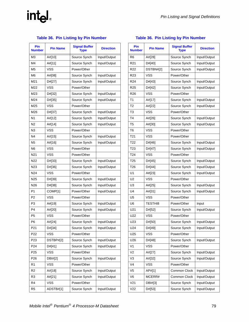
Pin Listing and Signal Definitions
M3 A#[10] Source Synch Input/Output
M4 A#[11] Source Synch Input/Output
M5 VSS Power/Other
M6 A#[08] Source Synch Input/Output
M21 D#[27] Source Synch Input/Output
M22 VSS Power/Other
M23 D#[32] Source Synch Input/Output
M24 D#[35] Source Synch Input/Output
M25 VSS Power/Other
M26 D#[37] Source Synch Input/Output
N1 A#[12] Source Synch Input/Output
N2 A#[14] Source Synch Input/Output
N3 VSS Power/Other
N4 A#[15] Source Synch Input/Output
N5 A#[16] Source Synch Input/Output
N6 VSS Power/Other
N21 VSS Power/Other
N22 D#[33] Source Synch Input/Output
N23 D#[36] Source Synch Input/Output
N24 VSS Power/Other
N25 D#[39] Source Synch Input/Output
N26 D#[38] Source Synch Input/Output
P1 COMP[1] Power/Other Input/Output
P2 VSS Power/Other
P3 A#[19] Source Synch Input/Output
P4 A#[20] Source Synch Input/Output
P5 VSS Power/Other
P6 A#[24] Source Synch Input/Output
P21 D#[34] Source Synch Input/Output
P22 VSS Power/Other
P23 DSTBP#[2] Source Synch Input/Output
P24 D#[41] Source Synch Input/Output
P25 VSS Power/Other
P26 DBI#[2] Source Synch Input/Output
R1 VSS Power/Other
R2 A#[18] Source Synch Input/Output
R3 A#[21] Source Synch Input/Output
R4 VSS Power/Other
R5 ADSTB#[1] Source Synch Input/Output
Table 36. Pin Listing by Pin Number
Pin Number Pin Name Signal Buffer
Type Direction
R6 A#[28] Source Synch Input/Output
R21 D#[40] Source Synch Input/Output
R22 DSTBN#[2] Source Synch Input/Output
R23 VSS Power/Other
R24 D#[43] Source Synch Input/Output
R25 D#[42] Source Synch Input/Output
R26 VSS Power/Other
T1 A#[17] Source Synch Input/Output
T2 A#[22] Source Synch Input/Output
T3 VSS Power/Other
T4 A#[26] Source Synch Input/Output
T5 A#[30] Source Synch Input/Output
T6 VSS Power/Other
T21 VSS Power/Other
T22 D#[46] Source Synch Input/Output
T23 D#[47] Source Synch Input/Output
T24 VSS Power/Other
T25 D#[45] Source Synch Input/Output
T26 D#[44] Source Synch Input/Output
U1 A#[23] Source Synch Input/Output
U2 VSS Power/Other
U3 A#[25] Source Synch Input/Output
U4 A#[31] Source Synch Input/Output
U5 VSS Power/Other
U6 TESTHI8 Power/Other Input
U21 D#[52] Source Synch Input/Output
U22 VSS Power/Other
U23 D#[50] Source Synch Input/Output
U24 D#[49] Source Synch Input/Output
U25 VSS Power/Other
U26 D#[48] Source Synch Input/Output
V1 VSS Power/Other
V2 A#[27] Source Synch Input/Output
V3 A#[32] Source Synch Input/Output
V4 VSS Power/Other
V5 AP#[1] Common Clock Input/Output
V6 MCERR# Common Clock Input/Output
V21 DBI#[3] Source Synch Input/Output
V22 D#[53] Source Synch Input/Output
Table 36. Pin Listing by Pin Number
Pin Number Pin Name Signal Buffer
Type Direction
Mobile Intel Pentium 4 Processor-M Datasheet 79

Pin Listing and Signal Definitions
V23 VSS Power/Other
V24 D#[54] Source Synch Input/Output
V25 D#[51] Source Synch Input/Output
V26 VSS Power/Other
W1 A#[29] Source Synch Input/Output
W2 A#[33] Source Synch Input/Output
W3 VSS Power/Other
W4 TESTHI9 Power/Other Input
W5 INIT# Asynch GTL+ Input
W6 VSS Power/Other
W21 VSS Power/Other
W22 DSTBN#[3] Source Synch Input/Output
W23 DSTBP#[3] Source Synch Input/Output
W24 VSS Power/Other
W25 D#[57] Source Synch Input/Output
W26 D#[55] Source Synch Input/Output
Y1 A#[34] Source Synch Input/Output
Y2 VSS Power/Other
Y3 TESTHI10 Power/Other Input
Y4 STPCLK# Asynch GTL+ Input
Y5 VSS Power/Other
Y6 BPM#[3] Common Clock Input/Output
Y21 D#[60] Source Synch Input/Output
Y22 VSS Power/Other
Y23 D#[58] Source Synch Input/Output
Y24 D#[59] Source Synch Input/Output
Y25 VSS Power/Other
Y26 D#[56] Source Synch Input/Output
Table 36. Pin Listing by Pin Number
Pin Number Pin Name Signal Buffer
Type Direction
80 Mobile Intel Pentium 4 Processor-M Datasheet

Pin Listing and Signal Definitions
5.2 Alphabetical Signals Reference
Table 37. Signal Description (Page 1 of 8)
Name Type Description
A[35:3]# Input/Output
A[35:3]# (Address) define a 236-byte physical memory address space. In sub-phase 1 of the address phase, these pins transmit the address of a transaction. In sub-phase 2, these pins transmit transaction type information. These signals must connect the appropriate pins of all agents on the Mobile Intel Pentium 4 Processor-M system bus. A[35:3]# are protected by parity signals AP[1:0]#. A[35:3]# are source synchronous signals and are latched into the receiving buffers by ADSTB[1:0]#.On the active-to-inactive transition of RESET#, the processor samples a subset of the A[35:3]# pins to determine power-on configuration. See Section 7.1 for more details.
A20M# Input
If A20M# (Address-20 Mask) is asserted, the processor masks physical address bit 20 (A20#) before looking up a line in any internal cache and before driving a read/write transaction on the bus. Asserting A20M# emulates the 8086 processor's address wrap-around at the 1-Mbyte boundary. Assertion of A20M# is only supported in real mode.A20M# is an asynchronous signal. However, to ensure recognition of this signal following an Input/Output write instruction, it must be valid along with the TRDY# assertion of the corresponding Input/Output Write bus transaction.
ADS# Input/Output
ADS# (Address Strobe) is asserted to indicate the validity of the transaction address on the A[35:3]# and REQ[4:0]# pins. All bus agents observe the ADS# activation to begin parity checking, protocol checking, address decode, internal snoop, or deferred reply ID match operations associated with the new transaction.
ADSTB[1:0]# Input/Output
Address strobes are used to latch A[35:3]# and REQ[4:0]# on their rising and falling edges. Strobes are associated with signals as shown below.
AP[1:0]# Input/Output
AP[1:0]# (Address Parity) are driven by the request initiator along with ADS#, A[35:3]#, and the transaction type on the REQ[4:0]#. A correct parity signal is high if an even number of covered signals are low and low if an odd number of covered signals are low. This allows parity to be high when all the covered signals are high. AP[1:0]# should connect the appropriate pins of all Mobile Intel Pentium 4 Processor-M system bus agents. The following table defines the coverage model of these signals.
BCLK[1:0] Input
The differential pair BCLK (Bus Clock) determines the system bus frequency. All processor system bus agents must receive these signals to drive their outputs and latch their inputs.All external timing parameters are specified with respect to the rising edge of BCLK0 crossing VCROSS.
Signals Associated Strobe
REQ[4:0]#, A[16:3]# ADSTB0#
A[35:17]# ADSTB1#
Request Signals subphase 1 subphase 2
A[35:24]# AP0# AP1#
A[23:3]# AP1# AP0#
REQ[4:0]# AP1# AP0#
Mobile Intel Pentium 4 Processor-M Datasheet 81

Pin Listing and Signal Definitions
BINIT# Input/Output
BINIT# (Bus Initialization) may be observed and driven by all processor system bus agents and if used, must connect the appropriate pins of all such agents. If the BINIT# driver is enabled during power-on configuration, BINIT# is asserted to signal any bus condition that prevents reliable future operation. If BINIT# observation is enabled during power-on configuration, and BINIT# is sampled asserted, symmetric agents reset their bus LOCK# activity and bus request arbitration state machines. The bus agents do not reset their IOQ and transaction tracking state machines upon observation of BINIT# activation. Once the BINIT# assertion has been observed, the bus agents will re-arbitrate for the system bus and attempt completion of their bus queue and IOQ entries.If BINIT# observation is disabled during power-on configuration, a central agent may handle an assertion of BINIT# as appropriate to the error handling architecture of the system.
BNR# Input/Output
BNR# (Block Next Request) is used to assert a bus stall by any bus agent who is unable to accept new bus transactions. During a bus stall, the current bus owner cannot issue any new transactions.
BPM[5:0]# Input/Output
BPM[5:0]# (Breakpoint Monitor) are breakpoint and performance monitor signals. They are outputs from the processor which indicate the status of breakpoints and programmable counters used for monitoring processor performance. BPM[5:0]# should connect the appropriate pins of all Mobile Intel Pentium 4 Processor-M system bus agents.BPM4# provides PRDY# (Probe Ready) functionality for the TAP port. PRDY# is a processor output used by debug tools to determine processor debug readiness.BPM5# provides PREQ# (Probe Request) functionality for the TAP port. PREQ# is used by debug tools to request debug operation of the processor.Please refer to the Mobile Intel Pentium 4 Processor-M and Intel 845MP/845MZ Chipset Platform Design Guide.These signals do not have on-die termination and must be terminated on the system board.
BPRI# Input
BPRI# (Bus Priority Request) is used to arbitrate for ownership of the processor system bus. It must connect the appropriate pins of all processor system bus agents. Observing BPRI# active (as asserted by the priority agent) causes all other agents to stop issuing new requests, unless such requests are part of an ongoing locked operation. The priority agent keeps BPRI# asserted until all of its requests are completed, then releases the bus by deasserting BPRI#.
BR0# Input/Output
BR0# drives the BREQ0# signal in the system and is used by the processor to request the bus. During power-on configuration this pin is sampled to determine the agent ID = 0. This signal does not have on-die termination and must be terminated.
BSEL[1:0] Output
BSEL[1:0] (Bus Select) are used to select the processor input clock frequency. Table 5 defines the possible combinations of the signals and the frequency associated with each combination. The required frequency is determined by the processor, chipset and clock synthesizer. All agents must operate at the same frequency. The Mobile Intel Pentium 4 Processor-M operates at a 400 MHz system bus frequency (100 MHz BCLK[1:0] frequency). For more information about these pins, including termination recommendations refer to Section 2.9 and the appropriate platform design guidelines.
COMP[1:0] AnalogCOMP[1:0] must be terminated on the system board using precision resistors. Refer to the Mobile Intel Pentium 4 Processor-M and Intel 845MP/845MZ Chipset Platform Design Guide for details on implementation.
Table 37. Signal Description (Page 2 of 8)
Name Type Description
82 Mobile Intel Pentium 4 Processor-M Datasheet

Pin Listing and Signal Definitions
D[63:0]# Input/Output
D[63:0]# (Data) are the data signals. These signals provide a 64-bit data path between the processor system bus agents, and must connect the appropriate pins on all such agents. The data driver asserts DRDY# to indicate a valid data transfer.D[63:0]# are quad-pumped signals and will thus be driven four times in a common clock period. D[63:0]# are latched off the falling edge of both DSTBP[3:0]# and DSTBN[3:0]#. Each group of 16 data signals correspond to a pair of one DSTBP# and one DSTBN#. The following table shows the grouping of data signals to data strobes and DBI#.
Furthermore, the DBI# pins determine the polarity of the data signals. Each group of 16 data signals corresponds to one DBI# signal. When the DBI# signal is active, the corresponding data group is inverted and therefore sampled active high.
DBI[3:0]# Input/Output
DBI[3:0]# (Data Bus Inversion) are source synchronous and indicate the polarity of the D[63:0]# signals. The DBI[3:0]# signals are activated when the data on the data bus is inverted. If more than half of the data bits, within a 16-bit group, would have been asserted electrically low, the bus agent may invert the data bus signals for that particular sub-phase for that 16-bit group.
DBR# OutputDBR# (Data Bus Reset) is used only in processor systems where no debug port is implemented on the system board. DBR# is used by a debug port interposer so that an in-target probe can drive system reset. If a debug port is implemented in the system, DBR# is a no connect in the system. DBR# is not a processor signal.
DBSY# Input/Output
DBSY# (Data Bus Busy) is asserted by the agent responsible for driving data on the processor system bus to indicate that the data bus is in use. The data bus is released after DBSY# is deasserted. This signal must connect the appropriate pins on all processor system bus agents.
DEFER# InputDEFER# is asserted by an agent to indicate that a transaction cannot be guaranteed in-order completion. Assertion of DEFER# is normally the responsibility of the addressed memory or Input/Output agent. This signal must connect the appropriate pins of all processor system bus agents.
DP[3:0]# Input/Output
DP[3:0]# (Data parity) provide parity protection for the D[63:0]# signals. They are driven by the agent responsible for driving D[63:0]#, and must connect the appropriate pins of all Mobile Intel Pentium 4 Processor-M system bus agents.
Table 37. Signal Description (Page 3 of 8)
Name Type Description
Quad-Pumped Signal Groups
Data Group DSTBN#/DSTBP# DBI#
D[15:0]# 0 0
D[31:16]# 1 1
D[47:32]# 2 2
D[63:48]# 3 3
DBI[3:0] Assignment To Data Bus
Bus Signal Data Bus Signals
DBI3# D[63:48]#
DBI2# D[47:32]#
DBI1# D[31:16]#
DBI0# D[15:0]#
Mobile Intel Pentium 4 Processor-M Datasheet 83

Pin Listing and Signal Definitions
DPSLP# InputDPSLP# when asserted on the platform causes the processor to transition from the Sleep State to the Deep Sleep state. In order to return to the Sleep State, DPSLP# must be deasserted and BCLK[1:0] must be running.
DRDY# Input/Output
DRDY# (Data Ready) is asserted by the data driver on each data transfer, indicating valid data on the data bus. In a multi-common clock data transfer, DRDY# may be deasserted to insert idle clocks. This signal must connect the appropriate pins of all processor system bus agents.
DSTBN[3:0]# Input/Output
Data strobe used to latch in D[63:0]#.
DSTBP[3:0]# Input/Output
Data strobe used to latch in D[63:0]#.
FERR#/PBE# Output
FERR#/PBE# (floating point error/pending break event) is a multiplexed signal and its meaning is qualified by STPCLK#. When STPCLK# is not asserted, FERR#/PBE# indicates a floating-point error and will be asserted when the processor detects an unmasked floating-point error. When STPCLK# is not asserted, FERR#/PBE# is similar to the ERROR# signal on the INTEL 387 coprocessor, and is included for compatibility with systems using MS-DOS*-type floating-point error reporting. When STPCLK# is asserted, an assertion of FERR#/PBE# indicates that the processor has a pending break event waiting for service. The assertion of FERR#/PBE# indicates that the processor should be returned to the Normal state. When FERR#/PBE# is asserted, indicating a break event, it will remain asserted until STPCLK# is deasserted. For additional information on the pending break event functionality, including the identification of support of the feature and enable/disable information, refer to volume 3 of the Intel Architecture Software Developer's Manual and the Intel Processor Identification and the CPUID Instruction application note.
GHI# Input
The GHI# signal controls the selection of the operating mode bus ratio and voltage in the Mobile Intel Pentium 4 Processor-M. On the Mobile Intel Pentium 4 Processor-M featuring Enhanced Intel SpeedStep technology, this signal is latched on entry to Sleep state and is observed during the Deep Sleep state. GHI# determines which of two performance states is selected for operation. This signal is ignored when the processor is not in the Deep Sleep state. This signal should be driven with an Open-drain driver. Refer to the Mobile Intel Pentium 4 Processor-M and Intel 845MP/845MZ Chipset Platform Design Guide for termination and connection guidelines.
GTLREF InputGTLREF determines the signal reference level for AGTL+ input pins. GTLREF should be set at 2/3 VCC. GTLREF is used by the AGTL+ receivers to determine if a signal is a logical 0 or logical 1. Refer to the Mobile Intel Pentium 4 Processor-M and Intel 845MP/845MZ Chipset Platform Design Guide for more information.
Table 37. Signal Description (Page 4 of 8)
Name Type Description
Signals Associated Strobe
D[15:0]#, DBI0# DSTBN0#
D[31:16]#, DBI1# DSTBN1#
D[47:32]#, DBI2# DSTBN2#
D[63:48]#, DBI3# DSTBN3#
Signals Associated Strobe
D[15:0]#, DBI0# DSTBP0#
D[31:16]#, DBI1# DSTBP1#
D[47:32]#, DBI2# DSTBP2#
D[63:48]#, DBI3# DSTBP3#
84 Mobile Intel Pentium 4 Processor-M Datasheet

Pin Listing and Signal Definitions
HIT#
HITM#
Input/Output
Input/Output
HIT# (Snoop Hit) and HITM# (Hit Modified) convey transaction snoop operation results. Any system bus agent may assert both HIT# and HITM# together to indicate that it requires a snoop stall, which can be continued by reasserting HIT# and HITM# together.
IERR# Output
IERR# (Internal Error) is asserted by a processor as the result of an internal error. Assertion of IERR# is usually accompanied by a SHUTDOWN transaction on the processor system bus. This transaction may optionally be converted to an external error signal (e.g., NMI) by system core logic. The processor will keep IERR# asserted until the assertion of RESET#. This signal does not have on-die termination and must be terminated on the system board.
IGNNE# Input
IGNNE# (Ignore Numeric Error) is asserted to force the processor to ignore a numeric error and continue to execute noncontrol floating-point instructions. If IGNNE# is deasserted, the processor generates an exception on a noncontrol floating-point instruction if a previous floating-point instruction caused an error. IGNNE# has no effect when the NE bit in control register 0 (CR0) is set.IGNNE# is an asynchronous signal. However, to ensure recognition of this signal following an Input/Output write instruction, it must be valid along with the TRDY# assertion of the corresponding Input/Output Write bus transaction.
INIT# Input
INIT# (Initialization), when asserted, resets integer registers inside the processor without affecting its internal caches or floating-point registers. The processor then begins execution at the power-on Reset vector configured during power-on configuration. The processor continues to handle snoop requests during INIT# assertion. INIT# is an asynchronous signal and must connect the appropriate pins of all processor system bus agents.If INIT# is sampled active on the active to inactive transition of RESET#, then the processor executes its Built-in Self-Test (BIST).
ITPCLKOUT [1:0] Output
ITPCLKOUT[1:0] is an uncompensated differential clock output that is a delayed copy of the BCLK[1:0], which is an input to the processor. This clock output can be used as the differential clock into the ITP port that is designed onto the motherboard. If ITPCLKOUT[1:0] outputs are not used, they must be terminated properly. Refer to Section 2.5 for additional details and termination requirements.
ITP_CLK[1:0] Input
ITP_CLK[1:0] are copies of BCLK that are used only in processor systems where no debug port is implemented on the system board. ITP_CLK[1:0] are used as BCLK[1:0] references for a debug port implemented on an interposer. If a debug port is implemented in the system, ITP_CLK[1:0] are no connects in the system. These are not processor signals.
LINT[1:0] Input
LINT[1:0] (Local APIC Interrupt) must connect the appropriate pins of all APIC Bus agents. When the APIC is disabled, the LINT0 signal becomes INTR, a maskable interrupt request signal, and LINT1 becomes NMI, a nonmaskable interrupt. INTR and NMI are backward compatible with the signals of those names on the Pentium processor. Both signals are asynchronous.Both of these signals must be software configured via BIOS programming of the APIC register space to be used either as NMI/INTR or LINT[1:0]. Because the APIC is enabled by default after Reset, operation of these pins as LINT[1:0] is the default configuration.
LOCK# Input/Output
LOCK# indicates to the system that a transaction must occur atomically. This signal must connect the appropriate pins of all processor system bus agents. For a locked sequence of transactions, LOCK# is asserted from the beginning of the first transaction to the end of the last transaction.When the priority agent asserts BPRI# to arbitrate for ownership of the processor system bus, it will wait until it observes LOCK# deasserted. This enables symmetric agents to retain ownership of the processor system bus throughout the bus locked operation and ensure the atomicity of lock.
Table 37. Signal Description (Page 5 of 8)
Name Type Description
Mobile Intel Pentium 4 Processor-M Datasheet 85

Pin Listing and Signal Definitions
MCERR# Input/Output
MCERR# (Machine Check Error) is asserted to indicate an unrecoverable error without a bus protocol violation. It may be driven by all processor system bus agents.MCERR# assertion conditions are configurable at a system level. Assertion options are defined by the following options:
Enabled or disabled.Asserted, if configured, for internal errors along with IERR#.Asserted, if configured, by the request initiator of a bus transaction after it observes an error.
Asserted by any bus agent when it observes an error in a bus transaction.For more details regarding machine check architecture, please refer to the IA-32 Software Developer’s Manual, Volume 3: System Programming Guide.
PROCHOT# Output The assertion of PROCHOT# (Processor Hot) indicates that the processor die temperature has reached its thermal limit. See Section 6 for more details.
PWRGOOD Input
PWRGOOD (Power Good) is a processor input. The processor requires this signal to be a clean indication that the clocks and power supplies are stable and within their specifications. ‘Clean’ implies that the signal will remain low (capable of sinking leakage current), without glitches, from the time that the power supplies are turned on until they come within specification. The signal must then transition monotonically to a high state. Figure 16 illustrates the relationship of PWRGOOD to the RESET# signal. PWRGOOD can be driven inactive at any time, but clocks and power must again be stable before a subsequent rising edge of PWRGOOD. It must also meet the minimum pulse width specification in Table 22, and be followed by a 1 to 10 ms RESET# pulse.The PWRGOOD signal must be supplied to the processor; it is used to protect internal circuits against voltage sequencing issues. It should be driven high throughout boundary scan operation.
REQ[4:0]# Input/Output
REQ[4:0]# (Request Command) must connect the appropriate pins of all processor system bus agents. They are asserted by the current bus owner to define the currently active transaction type. These signals are source synchronous to ADSTB0#. Refer to the AP[1:0]# signal description for details on parity checking of these signals.
RESET# Input
Asserting the RESET# signal resets the processor to a known state and invalidates its internal caches without writing back any of their contents. For a power-on Reset, RESET# must stay active for at least one millisecond after VCC and BCLK have reached their proper specifications. On observing active RESET#, all system bus agents will deassert their outputs within two clocks. RESET# must not be kept asserted for more than 10 ms while PWRGOOD is asserted.A number of bus signals are sampled at the active-to-inactive transition of RESET# for power-on configuration. These configuration options are described in the Section 7.1.This signal does not have on-die termination and must be terminated on the system board.
RS[2:0]# InputRS[2:0]# (Response Status) are driven by the response agent (the agent responsible for completion of the current transaction), and must connect the appropriate pins of all processor system bus agents.
RSP# Input
RSP# (Response Parity) is driven by the response agent (the agent responsible for completion of the current transaction) during assertion of RS[2:0]#, the signals for which RSP# provides parity protection. It must connect to the appropriate pins of all processor system bus agents.A correct parity signal is high if an even number of covered signals are low and low if an odd number of covered signals are low. While RS[2:0]# = 000, RSP# is also high, since this indicates it is not being driven by any agent guaranteeing correct parity.
Table 37. Signal Description (Page 6 of 8)
Name Type Description
86 Mobile Intel Pentium 4 Processor-M Datasheet

Pin Listing and Signal Definitions
SKTOCC# Output SKTOCC# (Socket Occupied) will be pulled to ground by the processor. System board designers may use this pin to determine if the processor is present.
SLP# Input
SLP# (Sleep), when asserted in Stop-Grant state, causes the processor to enter the Sleep state. During Sleep state, the processor stops providing internal clock signals to all units, leaving only the Phase-Locked Loop (PLL) still operating. Processors in this state will not recognize snoops or interrupts. The processor will only recognize the assertion of the RESET# signal, deassertion of SLP#, and assertion of DPSLP# input while in Sleep state. If SLP# is deasserted, the processor exits Sleep state and returns to Stop-Grant state, restarting its internal clock signals to the bus and processor core units. If the BCLK input is stopped or if DPSLP# is asserted while in the Sleep state, the processor will exit the Sleep state and transition to the Deep Sleep state.
SMI# Input
SMI# (System Management Interrupt) is asserted asynchronously by system logic. On accepting a System Management Interrupt, the processor saves the current state and enter System Management Mode (SMM). An SMI Acknowledge transaction is issued, and the processor begins program execution from the SMM handler.If SMI# is asserted during the deassertion of RESET# the processor will tristate its outputs.
STPCLK# Input
Assertion of STPCLK# (Stop Clock) causes the processor to enter a low power Stop-Grant state. The processor issues a Stop-Grant Acknowledge transaction, and stops providing internal clock signals to all processor core units except the system bus and APIC units. The processor continues to snoop bus transactions and service interrupts while in Stop-Grant state. When STPCLK# is deasserted, the processor restarts its internal clock to all units and resumes execution. The assertion of STPCLK# has no effect on the bus clock; STPCLK# is an asynchronous input.
TCK Input TCK (Test Clock) provides the clock input for the processor Test Bus (also known as the Test Access Port).
TDI Input TDI (Test Data In) transfers serial test data into the processor. TDI provides the serial input needed for JTAG specification support.
TDO Output TDO (Test Data Out) transfers serial test data out of the processor. TDO provides the serial output needed for JTAG specification support.
TESTHI[10:8]TESTHI[5:0]
Input TESTHI[10:8] and TESTHI[5:0] must be connected to a VCC power source through a resistor for proper processor operation. See Section 2.5 for more details.
THERMDA Other Thermal Diode Anode. See Section 6.
THERMDC Other Thermal Diode Cathode. See Section 6.
Table 37. Signal Description (Page 7 of 8)
Name Type Description
Mobile Intel Pentium 4 Processor-M Datasheet 87

Pin Listing and Signal Definitions
THERMTRIP# Output
Assertion of THERMTRIP# (Thermal Trip) indicates the processor junction temperature has reached a level beyond which permanent silicon damage may occur. Measurement of the temperature is accomplished through an internal thermal sensor which is configured to trip at approximately 135°C. Upon assertion of THERMTRIP#, the processor will shut off its internal clocks (thus halting program execution) in an attempt to reduce the processor junction temperature. To protect the processor, its core voltage (Vcc) must be removed following the assertion of THERMTRIP#. See Figure 19 and Table 22 for the appropriate power down sequence and timing requirements.For processors with CPUID of 0xF24:Once activated, THERMTRIP# remains latched until RESET# is asserted. While the assertion of the RESET# signal will de-assert THERMTRIP#, if the processor’s junction temperature remains at or above the trip level, THERMTRIP# will again be asserted.For processors with CPUID of 0xF27 or higher:Driving of the THERMTRIP# signal is enabled within 10 us of the assertion of PWRGOOD and is disabled on de-assertion of PWRGOOD. Once activated, THERMTRIP# remains latched until PWRGOOD is de-asserted. While the de-assertion of the PWRGOOD signal will de-assert THERMTRIP#, if the processor’s junction temperature remains at or above the trip level, THERMTRIP# will again be asserted within 10 us of the assertion of PWRGOOD.
TMS Input TMS (Test Mode Select) is a JTAG specification support signal used by debug tools.
TRDY# InputTRDY# (Target Ready) is asserted by the target to indicate that it is ready to receive a write or implicit writeback data transfer. TRDY# must connect the appropriate pins of all system bus agents.
TRST# Input TRST# (Test Reset) resets the Test Access Port (TAP) logic. TRST# must be driven low during power on Reset. This can be done with a 680 ohm pull-down resistor.
VCCA InputVCCA provides isolated power for the internal processor core PLL’s. Refer to the Mobile Intel Pentium 4 Processor-M and Intel 845MP/845MZ Chipset Platform Design Guide for complete implementation details.
VCCIOPLL InputVCCIOPLL provides isolated power for internal processor system bus PLL’s. Follow the guidelines for VCCA, and refer to the Mobile Intel Pentium 4 Processor-M and Intel 845MP/845MZ Chipset Platform Design Guide for complete implementation details.
VCCSENSE Output VCCSENSE is an isolated low impedance connection to processor core power (VCC). It can be used to sense or measure power near the silicon with little noise.
VCCVID Input Independent 1.2-V supply must be routed to VCCVID pin for the Mobile Intel Pentium 4 Processor-M’s Voltage Identification circuit.
VID[4:0] Output
VID[4:0] (Voltage ID) pins are used to support automatic selection of power supply voltages (Vcc). Unlike some previous generations of processors, these are open drain signals that are driven by the Mobile Intel Pentium 4 Processor-M and must be pulled up to 3.3 V (max.) with 1-Kohm resistors. The voltage supply for these pins must be valid before the VR can supply Vcc to the processor. Conversely, the VR output must be disabled until the voltage supply for the VID pins becomes valid. The VID pins are needed to support the processor voltage specification variations. See Table 3 for definitions of these pins. The VR must supply the voltage that is requested by the pins, or disable itself.
VSSA Input VSSA is the isolated ground for internal PLLs.
VSSSENSE Output VSSSENSE is an isolated low impedance connection to processor core VSS. It can be used to sense or measure ground near the silicon with little noise.
Table 37. Signal Description (Page 8 of 8)
Name Type Description
88 Mobile Intel Pentium 4 Processor-M Datasheet

Thermal Specifications and Design Considerations
6. Thermal Specifications and Design Considerations
In order to achieve proper cooling of the processor, a thermal solution (e.g., heat spreader, heat pipe, or other heat transfer system) must make firm contact to the exposed processor die. The processor die must be clean before the thermal solution is attached or the processor may be damaged.
Table 38 provides the Thermal Design Power (TDP) dissipation and the minimum and maximum TJ temperatures for the Mobile Intel Pentium 4 Processor-M. A thermal solution should be designed to ensure the junction temperature remains within the minimum and maximum TJ specifications while operating at the Thermal Design Power. Additionally, a secondary failsafe mechanism in hardware would be provided to shutdown the processor under catastrophic thermal conditions, as described in Section 2.4.3. TDP is a thermal design power specification based on the worst case power dissipation of the processor while executing publicly available software under normal operating conditions at nominal voltages. Contact your Intel Field Sales Representative for further information.
Table 38. Power Specifications for the Mobile Intel Pentium 4 Processor-M
NOTES:1. TDP is defined as the worst case power dissipated by the processor while executing publicly available
software under normal operating conditions at nominal voltages that meet the load line specifications. The TDP number shown is a specification based on ICC (maximum) at nominal voltages and indirectly tested by this ICC (maximum) testing. TDP definition is synonymous with the Thermal Design Power (typical) specification referred to in the previous EMTS. The Intel TDP specification is a recommended design point
Symbol Parameter Min Typ Max Unit Notes
TDP
Thermal Design Power at 2.6 GHz & 1.3 V 2.5 GHz & 1.3 V 2.4 GHz & 1.3 V 2.2 GHz & 1.3 V 2.0 GHz & 1.3 V 1.9 GHz & 1.3 V 1.8 GHz & 1.3 V 1.7 GHz & 1.3 V 1.6 GHz & 1.3 V 1.5 GHz & 1.3 V 1.4 GHz & 1.3 V 1.2 GHz & 1.2 V
35.035.035.035.032.032.030.030.030.026.925.820.8
W At 100°C, Note 1
PAH PSGNT PSLP
Auto Halt/Stop Grant/Sleep Power at 1.3 V (for >2.0 GHz) 1.3 V (for <= 2.0 GHz) 1.2 V
8.07.55.9
W At 50°C, Note 2
PDSLP
Deep Sleep Power at 1.3 V 1.2 V
5.04.2
W At 35°C, Note 2
PDPRSLPDeeper Sleep Power at 1.0 V 2.9
W At 35°C, Note 2
TJ Junction Temperature 0 100 °C Note 3
Mobile Intel Pentium 4 Processor-M Datasheet 89

Thermal Specifications and Design Considerations
and is not representative of the absolute maximum power the processor may dissipate under worst case conditions.
2. Not 100% tested. These power specifications are determined by characterization of the processor currents at higher temperatures and extrapolating the values for the temperature indicated.
3. The maximum junction temperature (TJ) is specified as the hottest location on the die. The thermal monitor’s automatic mode is used to indicate that the maximum TJ has been reached. Refer to Section 6.1.1 for TJ measurement guidelines (Refer to Section 6.1.2 for thermal monitor details).
6.1 Thermal Specifications
6.1.1 Thermal Diode
The Mobile Intel Pentium 4 Processor-M incorporates two methods of monitoring die temperature, the thermal monitor and the thermal diode. The thermal monitor (detailed in Section 6.1.2) must be used to determine when the minimum or maximum specified processor junction temperature has been reached. The second method, the thermal diode, can be read by an off-die analog/digital converter (a thermal sensor) located on the motherboard, or a stand-alone measurement kit. The thermal diode may be used to monitor the die temperature of the processor for thermal management or instrumentation purposes but cannot be used to indicate that the maximum TJ of the processor has been reached. Table 39 and Table 40 provide the diode interface and specifications.
Note: The reading of the thermal sensor connected to the thermal diode does not reflect the temperature of the hottest location on the die (TJ). This is due to inaccuracies in the thermal diode, on-die temperature gradients between the location of the thermal diode and the hottest location on the die, and time based variations in the die temperature. Time based variations can occur since the sampling rate of the sensor is much slower than the die level temperature changes.
The offset between the thermal diode based temperature reading and the hottest location of the die (thermal monitor) may be characterized using the thermal monitor’s Automatic mode activation of thermal control circuit. This temperature offset must be taken into account when using the processor thermal diode to implement power management events.
Table 39. Thermal Diode Interface
Table 40. Thermal Diode Specifications
NOTES:1. Intel does not support or recommend operation of the thermal diode under reverse bias.2. Characterized at 100°C.3. Not 100% tested. Specified by design characterization.4. The ideality factor, n, represents the deviation from ideal diode behavior as exemplified by the diode
equation: IFW=Is *(e(qVD/nkT) -1)
Signal Name Pin/Ball Number Signal Description
THERMDA B3 Thermal diode anode
THERMDC C4 Thermal diode cathode
Symbol Parameter Min Typ Max Unit Notes
IFW Forward Bias Current 5 300 µA 1
n Diode Ideality Factor 1.0012 1.0021 1.0030 2, 3, 4
RT Series Resistance 3.86 ohms 2, 3, 5
90 Mobile Intel Pentium 4 Processor-M Datasheet

Thermal Specifications and Design Considerations
Where IS = saturation current, q = electronic charge, VD = voltage across the diode, k = Boltzmann Constant, and T = absolute temperature (Kelvin).
5. The series resistance, RT, is provided to allow for a more accurate measurement of the diode junction temperature. RT as defined includes the pins of the processor but does not include any socket resistance or board trace resistance between the socket and the external remote diode thermal sensor. RT can be used by remote diode thermal sensors with automatic series resistance cancellation to calibrate out this error term. Another application is that a temperature offset can be manually calculated and programmed into an offset register in the remote diode thermal sensors as exemplified by the equation: Terror = [RT*(N-1)*IFWmin]/[(nk/q)*ln N] Where Terror = sensor temperature error, N = sensor current ration, k = Boltzmann Constant, q = electronic charge.
6.1.2 Thermal Monitor
The thermal monitor feature found in the Mobile Intel Pentium 4 Processor-M allows system designers to design lower cost thermal solutions without compromising system integrity or reliability. By using a factory-tuned, precision on-die thermal sensor, and a fast acting thermal control circuit (TCC), the processor, without the aid of any additional software or hardware, can keep the processor’s die temperature within factory specifications under nearly all conditions. The thermal monitor thus allows the processor and system thermal solutions to be designed much closer to the power envelopes of real applications, instead of being designed to the much higher maximum processor power envelopes.
The thermal monitor controls the processor temperature by modulating (starting and stopping) the processor core clocks. The processor clocks are modulated when the thermal control circuit (TCC) is activated. The thermal monitor uses two modes to activate the TCC: Automatic mode and On-Demand mode. Automatic mode is required for the processor to operate within specifications and must first be enabled via BIOS. Once automatic mode is enabled, the TCC will activate only when the internal die temperature is very near the temperature limits of the processor. When TCC is enabled, and a high temperature situation exists (i.e. TCC is active), the clocks will be modulated by alternately turning the clocks off and on at a duty cycle specific to the processor (typically 30-50%). An under-designed thermal solution that is not able to prevent excessive activation of the TCC in the anticipated ambient environment may cause a noticeable performance loss. Cycle times are processor speed dependent and will decrease linearly as processor core frequencies increase. Once the temperature has returned to a non-critical level, modulation ceases and TCC goes inactive. A small amount of hysteresis has been included to prevent rapid active/inactive transitions of the TCC when the processor temperature is near the trip point. Processor performance will be decreased by approximately the same amount as the duty cycle when the TCC is active, however, with a properly designed and characterized thermal solution, the TCC will only be activated briefly when running the most power intensive applications in a high ambient temperature environment.
For automatic mode, the duty cycle is factory configured and cannot be modified. Also, automatic mode does not require any additional hardware, software drivers or interrupt handling routines.
The TCC may also be activated via On-Demand mode. If bit 4 of the ACPI Thermal Monitor Control register is written to a 1 the TCC will be activated immediately, independent of the processor temperature. When using On-Demand mode to activate the TCC, the duty cycle of the clock modulation is programmable via bits 3:1 of the same ACPI Thermal Monitor Control register. In automatic mode, the duty cycle is fixed, however in On-Demand mode, the duty cycle can be programmed from 12.5% on/ 87.5% off, to 87.5% on/12.5% off in 12.5% increments. On-Demand mode may be used at the same time Automatic mode is enabled, however, if the system tries to enable the TCC via On-Demand mode at the same time automatic mode is enabled AND a high temperature condition exists, the duty cycle of the automatic mode will override the duty cycle selected by the On-Demand mode.
Mobile Intel Pentium 4 Processor-M Datasheet 91
Thermal Specifications and Design Considerations
An external signal, PROCHOT# (processor hot) is asserted when the processor die temperature has reached its thermal limit. If the TCC is enabled (note that the TCC must be enabled for the processor to be operating within spec), TCC will be active when the PROCHOT# signal is active. The temperature at which the thermal control circuit activates is not user configurable and is not software visible. Bus snooping and interrupt latching are active while the TCC is active.
Besides the thermal sensor and TCC, the thermal monitor feature also includes one ACPI register, performance monitoring logic, bits in three model specific registers (MSR), and one I/O pin (PROCHOT#). All are available to monitor and control the state of the thermal monitor feature. Thermal monitor can be configured to generate an interrupt upon the assertion or de-assertion of PROCHOT#.
If automatic mode is disabled the processor will be operating out of specification. Regardless of enabling of the automatic or On-Demand modes, in the event of a catastrophic cooling failure, the processor will automatically shut down when the silicon has reached a temperature of approximately 135 °C. At this point the system bus signal THERMTRIP# will go active and stay active until RESET# has been initiated. THERMTRIP# activation is independent of processor activity and does not generate any bus cycles. If THERMTRIP# is asserted, processor core voltage (VCC) must be removed within the timeframe defined in Table 22.
92 Mobile Intel Pentium 4 Processor-M Datasheet

Configuration and Low Power Features
7. Configuration and Low Power Features
7.1 Power-On Configuration Options
Several configuration options can be configured by hardware. The Mobile Intel Pentium 4 Processor-M samples its hardware configuration at reset, on the active-to-inactive transition of RESET#. For specifications on these options, please refer to Table 41.
Frequency determination functionality will exist on engineering sample processors which means that samples can run at varied frequencies. Production material will have the bus to core ratio locked during manufacturing and can only be operated at the rated frequency.
The sampled information configures the processor for subsequent operation. These configuration options cannot be changed except by another reset. All resets reconfigure the processor.
NOTE: Asserting this signal during RESET# will select the corresponding option.
7.2 Clock Control and Low Power States
The use of AutoHALT, Stop-Grant, Sleep, Deep Sleep and Deeper Sleep states is allowed in Mobile Intel Pentium 4 Processor-M based systems to reduce power consumption by stopping the clock to internal sections of the processor, depending on each particular state. See Figure 35 for a visual representation of the processor low-power states.
7.2.1 Normal State
This is the normal operating state for the processor.
7.2.2 AutoHALT Powerdown State
AutoHALT is a low-power state entered when the processor executes the HALT instruction. The processor will transition to the Normal state upon the occurrence of SMI#, BINIT#, INIT#, LINT[1:0] (NMI, INTR), or PSB interrupt message. RESET# will cause the processor to immediately initialize itself.
Table 41. Power-On Configuration Option PinsConfiguration Option Pin1
Output tristate SMI#Execute BIST INIT#In Order Queue pipelining (set IOQ depth to 1) A7#Disable MCERR# observation A9#Disable BINIT# observation A10#APIC Cluster ID (0-3) A[12:11]#Disable bus parking A15#Symmetric agent arbitration ID BR0#
Mobile Intel Pentium 4 Processor-M Datasheet 93

Configuration and Low Power Features
The return from a System Management Interrupt (SMI) handler can be to either Normal Mode or the AutoHALT Powerdown state. See the Intel Architecture Software Developer's Manual, Volume III: System Programmer's Guide for more information.
The system can generate a STPCLK# while the processor is in the AutoHALT Powerdown state. When the system deasserts the STPCLK# interrupt, the processor will return execution to the HALT state.
While in AutoHALT Powerdown state, the processor will process bus snoops.
7.2.3 Stop-Grant State
When the STPCLK# pin is asserted, the Stop-Grant state of the processor is entered 20 bus clocks after the response phase of the processor-issued Stop Grant Acknowledge special bus cycle.
Since the AGTL+ signal pins receive power from the system bus, these pins should not be driven (allowing the level to return to VCC) for minimum power drawn by the termination resistors in this state. In addition, all other input pins on the system bus should be driven to the inactive state.
BINIT# will not be serviced while the processor is in Stop-Grant state. The event will be latched and can be serviced by software upon exit from the Stop-Grant state.
RESET# will cause the processor to immediately initialize itself, but the processor will stay in Stop-Grant state. A transition back to the Normal state will occur with the de-assertion of the STPCLK# signal. When re-entering the Stop-Grant state from the Sleep state, STPCLK# should only be de-asserted ten or more bus clocks after the deassertion of SLP#.
A transition to the HALT/Grant Snoop state will occur when the processor detects a snoop on the system bus (see Section 7.2.4). A transition to the Sleep state (see Section 7.2.5) will occur with the assertion of the SLP# signal.
Figure 35. Clock Control States
snoopoccurs
StopGrantNormal Sleep
HALT/GrantSnoop
Auto Halt DeepSleep
STPCLK# asserted SLP# asserted
SLP# de-asserted
STPCLK# de-asserted
snoopserviced
HLTinstruction
snoopserviced snoop
occurs
DPSLP#de-asserted
DPSLP#asserted
STPCLK#asserted
STPCLK#de-asserted
haltbreak
V0001-04
core voltage raised
core voltage lowered
DeeperSleep
Halt break - A20M#, BINIT#, INIT#, INTR, NMI, PREQ#, RESET#, SMI#, or APIC interrupt
94 Mobile Intel Pentium 4 Processor-M Datasheet

Configuration and Low Power Features
While in the Stop-Grant State, SMI#, INIT#, BINIT# and LINT[1:0] will be latched by the processor, and only serviced when the processor returns to the Normal State. Only one occurrence of each event will be recognized upon return to the Normal state.
While in Stop-Grant state, the processor will process a system bus snoop.
7.2.4 HALT/Grant Snoop State
The processor will respond to snoop transactions on the system bus while in Stop-Grant state or in AutoHALT Power Down state. During a snoop transaction, the processor enters the HALT/Grant Snoop state. The processor will stay in this state until the snoop on the system bus has been serviced (whether by the processor or another agent on the system bus). After the snoop is serviced, the processor will return to the Stop-Grant state or AutoHALT Power Down state, as appropriate.
7.2.5 Sleep State
The Sleep state is a low power state in which the processor maintains its context, maintains the phase-locked loop (PLL), and has stopped all internal clocks. The Sleep state can only be entered from Stop-Grant state. Once in the Stop-Grant state, the processor will enter the Sleep state upon the assertion of the SLP# signal. The SLP# pin should only be asserted when the processor is in the Stop Grant state. SLP# assertions while the processor is not in the Stop-Grant state is out of specification and may result in unapproved operation.
Snoop events that occur while in Sleep State or during a transition into or out of Sleep state will cause unpredictable behaviour.
In the Sleep state, the processor is incapable of responding to snoop transactions or latching interrupt signals. No transitions or assertions of signals (with the exception of SLP#, DPSLP# or RESET#) are allowed on the system bus while the processor is in Sleep state. Any transition on an input signal before the processor has returned to Stop-Grant state will result in unpredictable behaviour.
If RESET# is driven active while the processor is in the Sleep state, and held active as specified in the RESET# pin specification, then the processor will reset itself, ignoring the transition through Stop-Grant State. If RESET# is driven active while the processor is in the Sleep State, the SLP# and STPCLK# signals should be deasserted immediately after RESET# is asserted to ensure the processor correctly executes the Reset sequence.
While in the Sleep state, the processor is capable of entering an even lower power state, the Deep Sleep state, by asserting the DPSLP# pin. (See Section 7.2.6.) Once in the Sleep or Deep Sleep states, the SLP# pin must be de-asserted if another asynchronous system bus event needs to occur. The SLP# pin has a minimum assertion of one BCLK period.
When the processor is in Sleep state, it will not respond to interrupts or snoop transactions.
7.2.6 Deep Sleep State
Deep Sleep state is a very low power state the processor can enter while maintaining context. Deep Sleep state is entered by asserting the DPSLP# pin. The DPSLP# pin must be de-asserted to re-enter the Sleep state. A period of 30 microseconds (to allow for PLL stabilization) must occur before the processor can be considered to be in the Sleep State. Once in the Sleep state, the SLP# pin can be deasserted to re-enter the Stop-Grant state.
Mobile Intel Pentium 4 Processor-M Datasheet 95

Configuration and Low Power Features
The clock may be stopped when the processor is in the Deep Sleep state in order to support the ACPI S1 state. The clock may only be stopped after DPSLP# is asserted and must be restarted before DPSLP# is deasserted. To provide maximum power conservation when stopping the clock during Deep Sleep, hold the BLCK0 input at VOL and the BCLK1 input at VOH.
While in Deep Sleep state, the processor is incapable of responding to snoop transactions or latching interrupt signals. No transitions of signals are allowed on the system bus while the processor is in Deep Sleep state. Any transition on an input signal before the processor has returned to Stop-Grant state will result in unpredictable behaviour.
7.2.7 Deeper Sleep State
The Deeper Sleep State is the lowest state power the processor can enter. This state is functionally identical to the Deep Sleep state but at a lower core voltage. The control signals to the voltage regulator to initiate a transition to the Deeper Sleep state are provided on the platform. Please refer the Mobile Intel Pentium 4 Processor-M and Intel 845MP/845MZ Chipset Platform Design Guide.
7.3 Enhanced Intel SpeedStep Technology
The Mobile Intel Pentium 4 Processor-M, when used in conjunction with the requisite Intel SpeedStep technology applet or its equivalent, supports Enhanced Intel SpeedStep technology. Enhanced Intel SpeedStep technology allows the processor to switch between two core frequencies automatically based on CPU demand, without having to reset the processor or change the system bus frequency. The processor has two bus ratios and voltages programmed into it instead of one and the GHI# signal controls which bus ratio and voltage is used. After reset, the processor will start in the lower of its two core frequencies, the “Battery Optimized” mode. An operating mode transition to the high core frequency can be made by setting GHI# low, putting the processor into the Deep Sleep state, regulating to the new VID output, and returning to the Normal state. This puts the processor into the high core frequency, or “Maximum Performance” operating mode. Going through these steps with GHI# set high, transitions the processor back to the low core frequency operating mode. The processor will drive the VID[4:0] pins with the VID of the current operating mode and the system logic is required to regulate the core voltage within specification for the driven VID.
96 Mobile Intel Pentium 4 Processor-M Datasheet

Debug Tools Specifications
8. Debug Tools Specifications
Please refer to the Mobile Intel Pentium 4 Processor-M and Intel 845MP/845MZ Chipset Platform Design Guide for information regarding debug tools specifications.
8.1 Logic Analyzer Interface (LAI)
Intel is working with two logic analyzer vendors to provide logic analyzer interfaces (LAIs) for use in debugging Mobile Intel Pentium 4 Processor-M systems. Tektronix* and Agilent* should be contacted to get specific information about their logic analyzer interfaces. The following information is general in nature. Specific information must be obtained from the logic analyzer vendor.
Due to the complexity of Mobile Intel Pentium 4 Processor-M systems, the LAI is critical in providing the ability to probe and capture system bus signals. There are two sets of considerations to keep in mind when designing a Mobile Intel Pentium 4 Processor-M system that can make use of an LAI: mechanical and electrical.
8.1.1 Mechanical Considerations
The LAI is installed between the processor socket and the Mobile Intel Pentium 4 Processor-M. The LAI pins plug into the socket, while the Mobile Intel Pentium 4 Processor-M pins plug into a socket on the LAI. Cabling that is part of the LAI egresses the system to allow an electrical connection between the Mobile Intel Pentium 4 Processor-M and a logic analyzer. The maximum volume occupied by the LAI, known as the keepout volume, as well as the cable egress restrictions, should be obtained from the logic analyzer vendor. System designers must make sure that the keepout volume remains unobstructed inside the system.
8.1.2 Electrical Considerations
The LAI will also affect the electrical performance of the system bus; therefore, it is critical to obtain electrical load models from each of the logic analyzer vendors to be able to run system level simulations to prove that their tool will work in the system. Contact the logic analyzer vendor for electrical specifications and load models for the LAI solution they provide.
Mobile Intel Pentium 4 Processor-M Datasheet 97