Embed Size (px)
Citation preview
MLX90614 family Single and Dual Zone
Infra Red Thermometer in TO-39
3901090614 Page 1 of 44 Data Sheet Rev 005 30 Mar 2009
Features and Benefits Small size, low cost Easy to integrate Factory calibrated in wide temperature range:
-40…+125 ˚C for sensor temperature and -70…+380 ˚C for object temperature.
High accuracy of 0.5°C over wide temperature range (0..+50°C for both Ta and To)
High (medical) accuracy calibration Measurement resolution of 0.02°C Single and dual zone versions SMBus compatible digital interface Customizable PWM output for continuous
reading Available in 3V and 5V versions Simple adaptation for 8…16V applications Power saving mode Different package options for applications and
measurements versatility Automotive grade
Applications Examples
High precision non-contact temperature measurements;
Thermal Comfort sensor for Mobile Air Conditioning control system;
Temperature sensing element for residential, commercial and industrial building air conditioning;
Windshield defogging; Automotive blind angle detection; Industrial temperature control of moving parts; Temperature control in printers and copiers; Home appliances with temperature control; Healthcare; Livestock monitoring; Movement detection; Multiple zone temperature control – up to 100
sensors can be read via common 2 wires Thermal relay / alert Body temperature measurement
Ordering Information Part No. MLX90614
Temperature Code E (-40°C to 85°C) K (-40°C to 125°C)
Package Code SF (TO-39)
- Option Code - X X X (1) (2) (3)
(1) Supply Voltage/ Accuracy A - 5V B - 3V C - Reserved D - 3V medical accuracy Example: MLX90614ESF-BAA
(2) Number of thermopiles: A – single zone B – dual zone C – gradient compensated* * : See page 2
(3) Package options: A – Standard package B – Reserved C – 35° FOV F – 10° FOV
1 Functional diagram
J1
CON1
SCL
SDA
GND
Vdd
C1 value and type may differin different applicationsfor optimum EMC
U1MLX906141
PWMSDA
C1
MLX90614 connection to SMBus
4Vss
SCLVz
MLX90614Axx: Vdd=4.5...5.5V
3
2
Vdd
0.1uF
Figure 1 Typical application schematics
2 General Description
The MLX90614 is an Infra Red thermometer for non contact temperature measurements. Both the IR sensitive thermopile detector chip and the signal conditioning ASSP are integrated in the same TO-39 can. Thanks to its low noise amplifier, 17-bit ADC and powerful DSP unit, a high accuracy and resolution of the thermometer is achieved. The thermometer comes factory calibrated with a digital PWM and SMBus (System Management Bus) output. As a standard, the 10-bit PWM is configured to continuously transmit the measured temperature in range of -20…120 ˚C, with an output resolution of 0.14 ˚C and the POR default is SMBus.

MLX90614 family Single and Dual Zone
Infra Red Thermometer in TO-39
3901090614 Page 2 of 44 Data Sheet Rev 005 30 Mar 2009
General description (continued)
The MLX90614 is built from 2 chips developed and manufactured by Melexis: • The Infra Red thermopile detector MLX81101 • The signal conditioning ASSP MLX90302, specially designed to process the output of IR sensor.
The device is available in an industry standard TO-39 package.
Thanks to the low noise amplifier, high resolution 17-bit ADC and powerful DSP unit of MLX90302 high accuracy and resolution of the thermometer is achieved. The calculated object and ambient temperatures are available in RAM of MLX90302 with resolution of 0.01 ˚C. They are accessible by 2 wire serial SMBus compatible protocol (0.02°C resolution) or via 10-bit PWM (Pulse Width Modulated) output of the device.
The MLX90614 is factory calibrated in wide temperature ranges: -40…125 ˚C for the ambient temperature and -70…382.2 ˚C for the object temperature.
The measured value is the average temperature of all objects in the Field Of View of the sensor. The MLX90614 offers a standard accuracy of ±0.5ºC around room temperatures. A special version for medical applications exists offering an accuracy of ±0.1ºC in a limited temperature range around the human body temperature.
It is very important for the application design to understand that these accuracies are only guaranteed and achievable when the sensor is in thermal equilibrium and under isothermal conditions (there are no temperature differences across the sensor package). The accuracy of the thermometer can be influenced by temperature differences in the package induced by causes like (among others): Hot electronics behind the sensor, heaters/coolers behind or beside the sensor or by a hot/cold object very close to the sensor that not only heats the sensing element in the thermometer but also the thermometer package.
This effect is especially relevant for thermometers with a small FOV like the -XXC and -XXF as the energy received by the sensor from the object is reduced. Therefore, Melexis has introduced the -XCX version of the MLX90614. In these MLX90614-XCX, the thermal gradients are measured internally and the measured temperature is compensated for them. In this way, the –XCX version of the MLX90614 is much less sensitive to thermal gradients, but the effect is not totally eliminated. It is therefore important to avoid the causes of thermal gradients as much as possible or to shield the sensor from them.
As a standard, the MLX90614 is calibrated for an object emissivity of 1. It can be easily customized by the customer for any other emissivity in the range 0.1…1.0 without the need of recalibration with a black body.
The 10-bit PWM is as a standard configured to transmit continuously the measured object temperature for an object temperature range of -20…120 ˚C with an output resolution of 0.14 ˚C. The PWM can be easily customized for virtually any range desired by the customer by changing the content of 2 EEPROM cells. This has no effect on the factory calibration of the device.
The PWM pin can also be configured to act as a thermal relay (input is To), thus allowing for an easy and cost effective implementation in thermostats or temperature (freezing/boiling) alert applications. The temperature threshold is user programmable. In a SMBus system this feature can act as a processor interrupt that can trigger reading all slaves on the bus and to determine the precise condition.
The thermometer is available in 2 supply voltage options: 5V compatible or 3V (battery) compatible. The 5V can be easily adopted to operate from a higher supply voltage (8…16V, for example) by use of few external components (refer to “Applications information” section for details).
An optical filter (long-wave pass) that cuts off the visible and near infra-red radiant flux is integrated in the package to provide ambient and sunlight immunity. The wavelength pass band of this optical filter is from 5.5 till 14µm.

MLX90614 family Single and Dual Zone
Infra Red Thermometer in TO-39
3901090614 Page 3 of 44 Data Sheet Rev 005 30 Mar 2009
3 Table of Contents
1 Functional diagram......................................................................................................................................................................................1 2 General Description ....................................................................................................................................................................................1 General description (continued) .....................................................................................................................................................................2 3 Table of Contents........................................................................................................................................................................................3 4 Glossary of Terms.......................................................................................................................................................................................4 5 Maximum ratings.........................................................................................................................................................................................4 6 Pin definitions and descriptions ..................................................................................................................................................................5 7 Electrical Specifications ..............................................................................................................................................................................6
7.1 MLX90614Axx .....................................................................................................................................................................................6 7.2 MLX90614Bxx, MLX90614Dxx............................................................................................................................................................8
8 Detailed description...................................................................................................................................................................................10 8.1 Block diagram....................................................................................................................................................................................10 8.2 Signal processing principle................................................................................................................................................................10 8.3 Block description ...............................................................................................................................................................................11
8.3.1 Amplifier .....................................................................................................................................................................................11 8.3.2 Supply regulator and POR .........................................................................................................................................................11 8.3.3 EEPROM....................................................................................................................................................................................11 8.3.4 RAM ...........................................................................................................................................................................................14
8.4 SMBus compatible 2-wire protocol ....................................................................................................................................................14 8.4.1 Functional description ................................................................................................................................................................14 8.4.2 Differences with the standard SMBus specification (reference [1]) ...........................................................................................15 8.4.3 Detailed description....................................................................................................................................................................15 8.4.4 AC specification for SMBus .......................................................................................................................................................17 8.4.5 Bit transfer..................................................................................................................................................................................18 8.4.6 Commands.................................................................................................................................................................................18 8.4.7 Sleep Mode................................................................................................................................................................................19
8.5 PWM..................................................................................................................................................................................................20 8.5.1 Single PWM format ....................................................................................................................................................................21 8.5.2 Extended PWM format ...............................................................................................................................................................22 8.5.3 Customizing the temperature range for PWM output.................................................................................................................23
8.6 Switching Between PWM and SMBus communication......................................................................................................................24 8.6.1 PWM is enabled.........................................................................................................................................................................24 8.6.2 Request condition ......................................................................................................................................................................24 8.6.3 PWM is disabled ........................................................................................................................................................................24
8.7 Computation of ambient and object temperatures.............................................................................................................................25 8.7.1 Ambient temperature Ta ............................................................................................................................................................25 8.7.2 Object temperature To ...............................................................................................................................................................25 8.7.3 Calculation flow..........................................................................................................................................................................25
8.8 Thermal relay.....................................................................................................................................................................................27 9 Unique Features........................................................................................................................................................................................28 10 Performance Graphs...............................................................................................................................................................................29
10.1 Temperature accuracy of the MLX90614 ........................................................................................................................................29 10.2 Field Of View (FOV) ........................................................................................................................................................................31
11 Applications Information..........................................................................................................................................................................33 11.1 Use of the MLX90614 thermometer in SMBus configuration ..........................................................................................................33 11.2 Use of multiple MLX90614s in SMBus configuration.......................................................................................................................33 11.3 PWM output operation.....................................................................................................................................................................34 11.4 Thermal alert / thermostat ...............................................................................................................................................................34 11.5 High voltage source operation.........................................................................................................................................................35
12 Application Comments ............................................................................................................................................................................36 13 Standard information regarding manufacturability of Melexis products with different soldering processes............................................38 14 ESD Precautions.....................................................................................................................................................................................38 15 FAQ.........................................................................................................................................................................................................39 16 Package Information ...............................................................................................................................................................................41
16.1 MLX90614XXA................................................................................................................................................................................41 16.2 MLX90614XCC................................................................................................................................................................................41 16.3 MLX90614XCF ................................................................................................................................................................................42 16.4 Part marking ....................................................................................................................................................................................42
17 References..............................................................................................................................................................................................43 18 Disclaimer ...............................................................................................................................................................................................43

MLX90614 family Single and Dual Zone
Infra Red Thermometer in TO-39
3901090614 Page 4 of 44 Data Sheet Rev 005 30 Mar 2009
4 Glossary of Terms
PTAT Proportional To Absolute Temperature sensor (package temperature) PTC Positive Temperature Coefficient sensor (package temperature) POR Power On Reset HFO High Frequency Oscillator (RC type) DSP Digital Signal Processing FIR Finite Impulse Response. Digital filter IIR Infinite Impulse Response. Digital filter IR Infra-Red PWM Pulse With Modulation DC Duty Cycle (of the PWM) ; Direct Current (for settled conditions specifications) FOV Field Of View SDA,SCL Serial DAta, Serial CLock – SMBus compatible communication pins Ta Ambient Temperature measured from the chip – (the package temperature) To Object Temperature, ‘seen’ from IR sensor ESD Electro-Static Discharge EMC Electro-Magnetic Compatibility ASSP Application Specific Standard Product TBD To Be Defined
Note: sometimes the MLX90614xxx is referred to as “the module”.
5 Maximum ratings
Parameter MLX90614ESF-Axx
MLX90614ESF-Bxx MLX90614ESF-Dxx
MLX90614KSF-Axx
Supply Voltage, VDD (over voltage) 7V 5V 7V Supply Voltage, VDD (operating) 5.5 V 3.6V 5.5V Reverse Voltage 0.4 V Operating Temperature Range, TA -40…+85°C -40…+125°C Storage Temperature Range, TS -40…+125°C -40…+125°C ESD Sensitivity (AEC Q100 002) 2kV DC current into SCL / Vz (Vz mode) 2 mA DC sink current, SDA / PWM pin 25 mA DC source current, SDA / PWM pin 25 mA DC clamp current, SDA / PWM pin 25 mA DC clamp current, SCL pin 25 mA
Table 1: Absolute maximum ratings for MLX90614
Exceeding the absolute maximum ratings may cause permanent damage. Exposure to absolute-maximum-rated conditions for extended periods may affect device reliability.
MLX90614 family Single and Dual Zone
Infra Red Thermometer in TO-39
3901090614 Page 5 of 44 Data Sheet Rev 005 30 Mar 2009
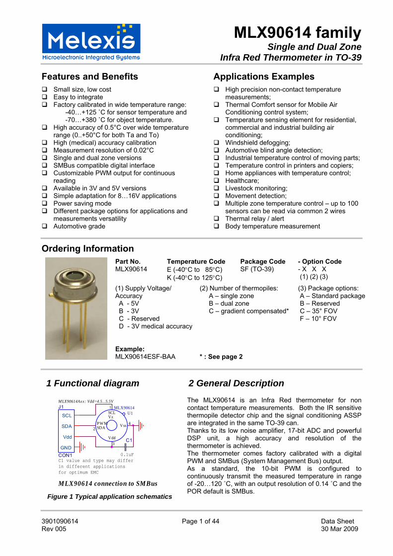
6 Pin definitions and descriptions
Figure 2: Pin description
Pin Name Function
VSS Ground. The metal can is also connected to this pin.
SCL / Vz Serial clock input for 2 wire communications protocol. 5.7V zener is available at this pin for connection of external bipolar transistor to MLX90614A to supply the device from external 8 …16V source.
PWM / SDA Digital input / output. In normal mode the measured object temperature is available at this pin Pulse Width Modulated. In SMBus compatible mode automatically configured as open drain NMOS.
VDD External supply voltage.
Table 2: Pin description MLX90614
Note: for +12V (+8…+16V) powered operation refer to the Application information section. For EMC and isothermal conditions reasons it is highly recommended not to use any electrical connection to the metal can except by the VSS pin. With the SCL / Vz and PWM / SDA pins operated in 2-wire interface mode, the input Schmidt trigger function is automatically enabled.
Top view
4 - VSS
2 - PWM / SDA 1 - SCL / Vz
3 - VDD
MLX90614 family Single and Dual Zone
Infra Red Thermometer in TO-39
3901090614 Page 6 of 44 Data Sheet Rev 005 30 Mar 2009
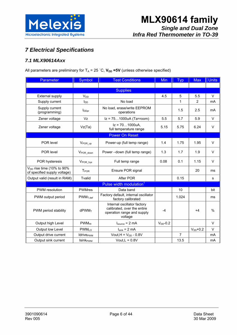
7 Electrical Specifications
7.1 MLX90614Axx
All parameters are preliminary for TA = 25 ˚C, VDD =5V (unless otherwise specified)
Parameter Symbol Test Conditions Min Typ Max Units
Supplies External supply VDD 4.5 5 5.5 V Supply current IDD No load 1 2 mA
Supply current (programming) IDDpr
No load, erase/write EEPROM operations 1.5 2.5 mA
Zener voltage Vz Iz = 75…1000uA (Ta=room) 5.5 5.7 5.9 V
Zener voltage Vz(Ta) Iz = 70…1000uA, full temperature range 5.15 5.75 6.24 V
Power On Reset
POR level VPOR_up Power-up (full temp range) 1.4 1.75 1.95 V
POR level VPOR_down Power –down (full temp range) 1.3 1.7 1.9 V
POR hysteresis VPOR_hys Full temp range 0.08 0.1 1.15 V
VDD rise time (10% to 90% of specified supply voltage) TPOR Ensure POR signal 20 ms
Output valid (result in RAM) Tvalid After POR 0.15 s
Pulse width modulation1 PWM resolution PWMres Data band 10 bit
PWM output period PWMT,def Factory default, internal oscillator
factory calibrated 1.024 ms
PWM period stability dPWMT
Internal oscillator factory calibrated, over the entire
operation range and supply voltage
-4 +4 %
Output high Level PWMHI Isource = 2 mA VDD-0.2 V
Output low Level PWMLO Isink = 2 mA VSS+0.2 V Output drive current IdrivePWM Vout,H = VDD - 0.8V 7 mA Output sink current IsinkPWM Vout,L = 0.8V 13.5 mA

MLX90614 family Single and Dual Zone
Infra Red Thermometer in TO-39
3901090614 Page 7 of 44 Data Sheet Rev 005 30 Mar 2009
Parameter Symbol Test Conditions Min Typ Max Units
SMBus compatible 2-wire interface2
Input high voltage VIH (Ta, V) Over temperature and supply VDD-0.1 V Input low voltage VIL (Ta, V) Over temperature and supply 0.6 V
Output low voltage VOL SDA pin in open drain mode, over temperature and supply,
Isink = 2mA 0.2 V
SCL leakage ISCL, leak VSCL=4V, Ta=+85°C 30 uA SDA leakage ISDA, leak VSDA=4V, Ta=+85°C 0.3 uA
SCL capacitance CSCL 10 pF SDA capacitance CSDA 10 pF
Slave address SA Factory default 5A hex Wake up request twake SDA low 33 ms SMBus Request tREQ SCL low 1.44 ms
Timeout, low Timeout,L SCL low 27 33 ms
Timeout, high Timeout,H SCL high 45 55 us Acknowledge setup time Tsuac(MD) 8-th SCL falling edge, Master 0.5 1.5 us Acknowledge hold time Thdac(MD) 9-th SCL falling edge, Master 1.5 2.5 us
Acknowledge setup time Tsuac(SD) 8-th SCL falling edge, Slave 2.5 us Acknowledge hold time Thdac(SD) 9-th SCL falling edge, Slave 1.5 us
EEPROM Data retention Ta = +85°C 10 years
Erase/write cycles Ta = +25°C 100,000 TimesErase/write cycles Ta = +125°C 10,000 Times
Erase cell time Terase 5 ms Write cell time Twrite 5 ms
Notes: All the communication and refresh rate timings are given for the nominal calibrated HFO frequency and will vary with this frequency’s variations. 1. All PWM timing specifications are given for single PWM output (factory default for MLX90614xAx). For the extended PWM output (factory default for the MLX90614xBx) each period has twice the timing specifications (refer to the PWM detailed description section). With large capacitive load lower PWM frequency is recommended. Thermal relay output (when configured) has the PWM DC specification and can be programmed as push-pull, or NMOS open drain. PWM is free-running, power-up factory default is SMBus, refer to 7.6, “Switching between PWM and SMBus communication” for details.. 2. For SMBus compatible interface on 12V application refer to Application information section. SMBus compatible interface is described in details in the SMBus detailed description section. Maximum number of MLX90614xxx devices on one bus is 127, higher pull-up currents are recommended for higher number of devices, faster bus data transfer rates, and increased reactive loading of the bus. MLX90614xxx is always a slave device on the bus. MLX90614xxx can work in both low-power and high-power SMBus communication. All voltages are referred to the Vss (ground) unless otherwise noted. Power saving mode is not available on the 5V version (MLX90614Axx).

MLX90614 family Single and Dual Zone
Infra Red Thermometer in TO-39
3901090614 Page 8 of 44 Data Sheet Rev 005 30 Mar 2009
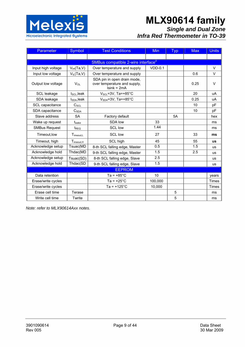
7.2 MLX90614Bxx, MLX90614Dxx
All parameters are preliminary for TA = 25 ˚C, VDD =3V (unless otherwise specified)
Parameter Symbol Test Conditions Min Typ Max Units
Supplies External supply VDD 2.6 3 3.6 V Supply current IDD No load 1 2 mA
Supply current (programming) IDDpr
No load, erase/write EEPROM operations 1.5 2.5 mA
Power-down supply t
Isleep no load 1 2.5 5 uA Power-down supply current Isleep Full temperature range 1 2.5 6 uA
Power On Reset POR level VPOR_up Power-up (full temp range) 1.4 1.75 1.95 V
POR level VPOR_down Power –down (full temp range) 1.3 1.7 1.9 V POR hysteresis VPOR_hys Full temp range 0.08 0.1 1.15 V VDD rise time (10% to 90% of specified supply voltage)
TPOR Ensure POR signal 20 ms
Output valid Tvalid After POR 0.15 s Pulse width modulation1
PWM resolution PWMres Data band 10 bit
PWM output period PWMT,def Factory default, internal oscillator
factory calibrated 1.024 ms
PWM period stability dPWMT
Internal oscillator factory calibrated, over the entire
operation range and supply voltage
-4 +4 %
Output high Level PWMHI Isource = 2 mA VDD-0.25 V Output low Level PWMLO Isink = 2 mA VSS+0.25 V Output drive current IdrivePWM Vout,H = VDD - 0.8V 4.5 mA Output sink current IsinkPWM Vout,L = 0.8V 11 mA
MLX90614 family Single and Dual Zone
Infra Red Thermometer in TO-39
3901090614 Page 9 of 44 Data Sheet Rev 005 30 Mar 2009
Parameter Symbol Test Conditions Min Typ Max Units
SMBus compatible 2-wire interface2
Input high voltage VIH(Ta,V) Over temperature and supply VDD-0.1 V Input low voltage VIL(Ta,V) Over temperature and supply 0.6 V
Output low voltage VOL SDA pin in open drain mode, over temperature and supply,
Isink = 2mA 0.25 V
SCL leakage ISCL,leak VSCL=3V, Ta=+85°C 20 uA SDA leakage ISDA,leak VSDA=3V, Ta=+85°C 0.25 uA
SCL capacitance CSCL 10 pF SDA capacitance CSDA 10 pF
Slave address SA Factory default 5A hex Wake up request twake SDA low 33 ms SMBus Request tREQ SCL low 1.44 ms
Timeout,low Timeout,L SCL low 27 33 ms
Timeout, high Timeout,H SCL high 45 55 us Acknowledge setup
tiTsuac(MD
)8-th SCL falling edge, Master 0.5 1.5 us
Acknowledge hold ti
Thdac(MD)
9-th SCL falling edge, Master 1.5 2.5 us Acknowledge setup
tiTsuac(SD) 8-th SCL falling edge, Slave 2.5 us
Acknowledge hold ti
Thdac(SD)
9-th SCL falling edge, Slave 1.5 us EEPROM
Data retention Ta = +85°C 10 years Erase/write cycles Ta = +25°C 100,000 TimesErase/write cycles Ta = +125°C 10,000 Times
Erase cell time Terase 5 ms Write cell time Twrite 5 ms
Note: refer to MLX90614Axx notes.

MLX90614 family Single and Dual Zone
Infra Red Thermometer in TO-39
3901090614 Page 10 of 44 Data Sheet Rev 005 30 Mar 2009
8 Detailed description
8.1 Block diagram
Figure 3: block diagram
8.2 Signal processing principle
The operation of the MLX90614 is controlled by an internal state machine, which controls the measurements and calculations of the object and ambient temperatures and does the post-processing of the temperatures to output them through the PWM output or the SMBus compatible interface. The ASSP supports 2 IR sensors (second one not implemented in the MLX90614xAx).The output of the IR sensors is amplified by a low noise low offset chopper amplifier with programmable gain, converted by a Sigma Delta modulator to a single bit stream and fed to a powerful DSP for further processing. The signal is treated by programmable (by means of EEPROM contend) FIR and IIR low pass filters for further reduction of the band width of the input signal to achieve the desired noise performance and refresh rate. The output of the IIR filter is the measurement result and is available in the internal RAM. 3 different cells are available: One for the on-board temperature sensor (on chip PTAT or PTC) and 2 for the IR sensors. Based on results of the above measurements, the corresponding ambient temperature Ta and object temperatures To are calculated. Both calculated temperatures have a resolution of 0.01 ˚C. The data for Ta and To can be read in two ways: Reading RAM cells dedicated for this purpose via the 2-wire interface (0.02°C resolution, fixed ranges), or through the PWM digital output (10 bit resolution, configurable range). In the last step of the measurement cycle, the measured Ta and To are rescaled to the desired output resolution of the PWM) and the recalculated data is loaded in the registers of the PWM state machine, which creates a constant frequency with a duty cycle representing the measured data.
81101
OPA ADC DSP PWM
STATE MACHINE
t°
Voltage Regulator 90302

MLX90614 family Single and Dual Zone
Infra Red Thermometer in TO-39
3901090614 Page 11 of 44 Data Sheet Rev 005 30 Mar 2009
8.3 Block description
8.3.1 Amplifier
A low noise low offset amplifier with programmable gain is implemented for amplification of the IR sensor voltage. With a carefully designed input modulator and balanced input impedance, an offset as low as 0.5µV is achieved.
8.3.2 Supply regulator and POR
The module can operate from 3 different supplies: VDD= 5V => MLX90614Axx VDD=3.3V => MLX90614Bxx (battery or regulated supply) VDD=8…16V => MLX90614Axx few external components are necessary please refer to “Applications information” section for information about adopting higher voltage supplies. The Power On Reset (POR) is connected to Vdd supply. The on-chip POR circuit provides an active (high) level of the POR signal when the Vdd voltage rises above approximately 0.5V and holds the entire MLX90614xxx in reset until the Vdd is higher than the specified POR threshold VPOR (note that this level is different for MLX90614Axx and MLX90614Bxx). During the time POR is active, the POR signal is available as an open drain at the PWM/SDA pin. After the MLX90614xxx exits the POR condition, the function programmed in EEPROM takes precedence for that pin.
8.3.3 EEPROM
A limited number of addresses in the EEPROM memory can be changed by the customer. The whole EEPROM can be read via SMBus interface.
EEPROM (32X16) Name Address Write acces
Tomax 000h Yes Tomin 001h Yes PWMCTRL 002h Yes Ta range 003h Yes Emissivity correction coefficient 004h Yes Config Register1 005h Yes
Melexis reserved 006h No … … …
Melexis reserved 00Dh No SMBus address 00Eh Yes
Melexis reserved 00Fh Yes Melexis reserved 010h No
… … … Melexis reserved 018h No Melexis reserved 019h Yes Melexis reserved 01Ah No Melexis reserved 01Bh No
ID number 01Ch No ID number 01Dh No ID number 01Eh No ID number 01Fh No
The addresses Tomax, Tomin and Ta range are for customer dependent object and ambient temperature ranges. For details see section 8.5.3 below in this document The address Emissivity contains the object emissivity (factory default 1.0 = 0xFFFF), 16 bit.
Emissivity = dec2hex[ round( 65535 x ε) ] Where dec2hex[ round( X ) ] represents decimal to hexadecimal conversion with round-off to nearest value (not truncation). In this case the physical emissivity values are ε = 0.1…1.0. Erase (write 0) must take place before write of desired data is made.

MLX90614 family Single and Dual Zone
Infra Red Thermometer in TO-39
3901090614 Page 12 of 44 Data Sheet Rev 005 30 Mar 2009
PWM period configuration: Period in extended PWM mode is twice the period in single PWM mode. In single PWM mode period is T = 1.024*P [ms], where P is the number, written in bits 15..9 PWMCTRL. Maximum period is then 131.072 ms for single and 262.144 ms for extended. These values are typical and depend on the on-chip RC oscillator absolute value. The duty cycle must be calculated instead of working only with the high time only in order to avoid errors from the period absolute value deviations. The address PWMCTRL consists of control bits for configuring the PWM/SDA pin as follows:
* Values are for nominal HFO frequency The address ConfigRegister1 consists of control bits for configuring the analog and digital parts:
Note: The following bits/registers should not be altered (except with special tools – contact Melexis for such tools availability) in order to keep the factory calibration relevant: Ke [15..0] ; Config Register1 [13..11;7;3] ; addresses 00Fh and 019h. Check www.melexis.com for latest application notes with details on EEPROM settings.

MLX90614 family Single and Dual Zone
Infra Red Thermometer in TO-39
3901090614 Page 13 of 44 Data Sheet Rev 005 30 Mar 2009
On-chip filtering and settling time: The MLX90614 features configurable on-chip digital filters. They allow customization for speed or noise. Factory default configurations and the typical settling time and noise for the MLX90614 family are given below.
Device Settling time, sec Typical noise, °C rms Spike limit MLX90614 AAA, BAA, DAA 0.10 0.05 100% MLX90614 ABA, BBA 0.14 0.07 100% MLX90614 ACC, BCC 0.14 0.18 100% MLX90614 ACF, BCF 1.33 0.10 50%
Details on the filters are given in the application note “Understanding MLX90614 on-chip digital signal filters” available from www.melexis.com . The evaluation board, EVB90614 supported by PC SW allows easy configuration of the filters, while not requiring in-depth understanding of the EEPROM. The available filter settings and the settling times they give are listed below. Settling time depends on three configurations: single/dual zone, IIR filter settings and FIR filter settings. The FIR filter has a straightforward effect on noise (a 4 times decrease of settling time increases the noise 2 times and vice versa). The IIR filter provides an additional, spike limiting, feature. Spike limit is also listed and defines to what level the magnitude of a spike would be limited – for example, 25% denotes that if a 20°C temperature delta spike is measured the temperature reading by the MLX90614 will spike only 5°C. More details are available in the application notes from www.melexis.com
IIR setting FIR setting Settling time (s) 90614xAx
Settling time (s) 90614xBx, 90614xCx Spike limit
xxx 000…011 Not recommended 100 100 0.04 0.06 100.0% 100 101 0.05 0.07 100.0% 100 110 0.06 0.10 100.0% 100 111 0.10 0.14 100.0% 101 100 0.12 0.20 80.0% 101 101 0.16 0.24 80.0% 101 110 0.22 0.34 80.0% 101 111 0.35 0.54 80.0% 110 100 0.24 0.38 66.7% 110 101 0.30 0.48 66.7% 110 110 0.43 0.67 66.7% 110 111 0.70 1.10 66.7% 111 100 0.26 0.42 57.0% 111 101 0.34 0.53 57.0% 111 110 0.48 0.75 57.0% 111 111 0.78 1.20 57.0% 000 100 0.30 0.47 50.0% 000 101 0.37 0.60 50.0% 000 110 0.54 0.84 50.0% 000 111 0.86 1.33 50.0% 001 100 0.70 1.10 25.0% 001 101 0.88 1.40 25.0% 001 110 1.30 2.00 25.0% 001 111 2.00 3.20 25.0% 010 100 1.10 1.80 16.7% 010 101 1.40 2.20 16.7% 010 110 2.00 3.20 16.7% 010 111 3.30 5.00 16.7% 011 100 1.50 2.40 12.5% 011 101 1.90 3.00 12.5% 011 110 2.80 4.30 12.5% 011 111 4.50 7.00 12.5%
Note: Settling time is in seconds and depends on internal oscillator absolute value. 100% spike limit appears with the IIR filter bypassed, and there is no spike limitation.
MLX90614 family Single and Dual Zone
Infra Red Thermometer in TO-39
3901090614 Page 14 of 44 Data Sheet Rev 005 30 Mar 2009
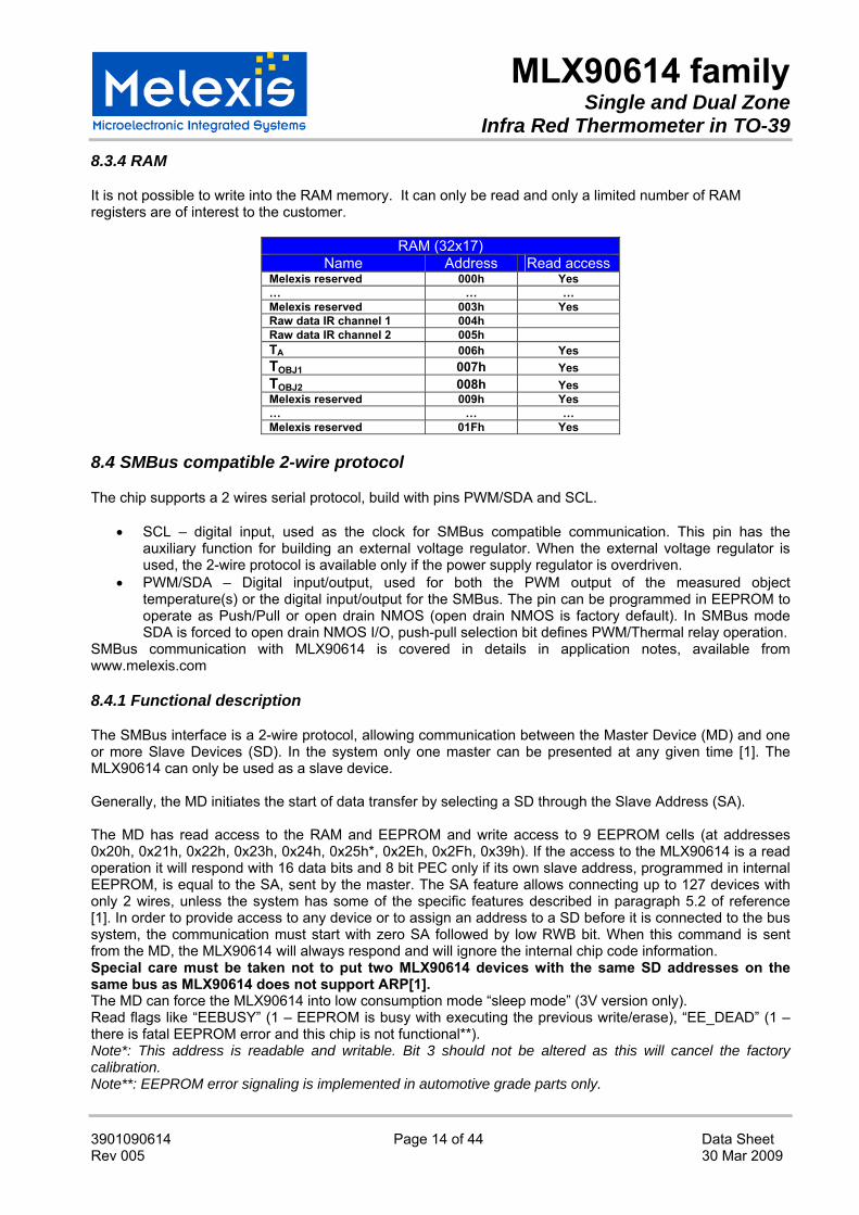
8.3.4 RAM
It is not possible to write into the RAM memory. It can only be read and only a limited number of RAM registers are of interest to the customer.
RAM (32x17) Name Address Read access
Melexis reserved 000h Yes … … … Melexis reserved 003h Yes Raw data IR channel 1 004h Raw data IR channel 2 005h TA 006h Yes TOBJ1 007h Yes TOBJ2 008h Yes Melexis reserved 009h Yes … … … Melexis reserved 01Fh Yes
8.4 SMBus compatible 2-wire protocol
The chip supports a 2 wires serial protocol, build with pins PWM/SDA and SCL.
• SCL – digital input, used as the clock for SMBus compatible communication. This pin has the auxiliary function for building an external voltage regulator. When the external voltage regulator is used, the 2-wire protocol is available only if the power supply regulator is overdriven.
• PWM/SDA – Digital input/output, used for both the PWM output of the measured object temperature(s) or the digital input/output for the SMBus. The pin can be programmed in EEPROM to operate as Push/Pull or open drain NMOS (open drain NMOS is factory default). In SMBus mode SDA is forced to open drain NMOS I/O, push-pull selection bit defines PWM/Thermal relay operation.
SMBus communication with MLX90614 is covered in details in application notes, available from www.melexis.com
8.4.1 Functional description
The SMBus interface is a 2-wire protocol, allowing communication between the Master Device (MD) and one or more Slave Devices (SD). In the system only one master can be presented at any given time [1]. The MLX90614 can only be used as a slave device. Generally, the MD initiates the start of data transfer by selecting a SD through the Slave Address (SA). The MD has read access to the RAM and EEPROM and write access to 9 EEPROM cells (at addresses 0x20h, 0x21h, 0x22h, 0x23h, 0x24h, 0x25h*, 0x2Eh, 0x2Fh, 0x39h). If the access to the MLX90614 is a read operation it will respond with 16 data bits and 8 bit PEC only if its own slave address, programmed in internal EEPROM, is equal to the SA, sent by the master. The SA feature allows connecting up to 127 devices with only 2 wires, unless the system has some of the specific features described in paragraph 5.2 of reference [1]. In order to provide access to any device or to assign an address to a SD before it is connected to the bus system, the communication must start with zero SA followed by low RWB bit. When this command is sent from the MD, the MLX90614 will always respond and will ignore the internal chip code information. Special care must be taken not to put two MLX90614 devices with the same SD addresses on the same bus as MLX90614 does not support ARP[1]. The MD can force the MLX90614 into low consumption mode “sleep mode” (3V version only). Read flags like “EEBUSY” (1 – EEPROM is busy with executing the previous write/erase), “EE_DEAD” (1 – there is fatal EEPROM error and this chip is not functional**). Note*: This address is readable and writable. Bit 3 should not be altered as this will cancel the factory calibration. Note**: EEPROM error signaling is implemented in automotive grade parts only.
MLX90614 family Single and Dual Zone
Infra Red Thermometer in TO-39
3901090614 Page 15 of 44 Data Sheet Rev 005 30 Mar 2009
8.4.2 Differences with the standard SMBus specification (reference [1])
There are eleven command protocols for standard SMBus interface. The MLX90614 supports only two of them. Not supported commands are:
• Quick Command • Byte commands - Sent Byte, Receive Byte, Write Byte and Read Byte • Process Call • Block commands – Block Write and Write-Block Read Process Call
Supported commands are: • Read Word • Write Word
8.4.3 Detailed description
The PWM/SDA pin of MLX90614 can operate also as PWM output, depending on the EEPROM settings. If PWM is enabled, after POR the PWM/SDA pin is directly configured as PWM output. The PWM mode can be avoided and the pin can be restored to its Data function by a special command. That is why hereafter both modes are treated separately.
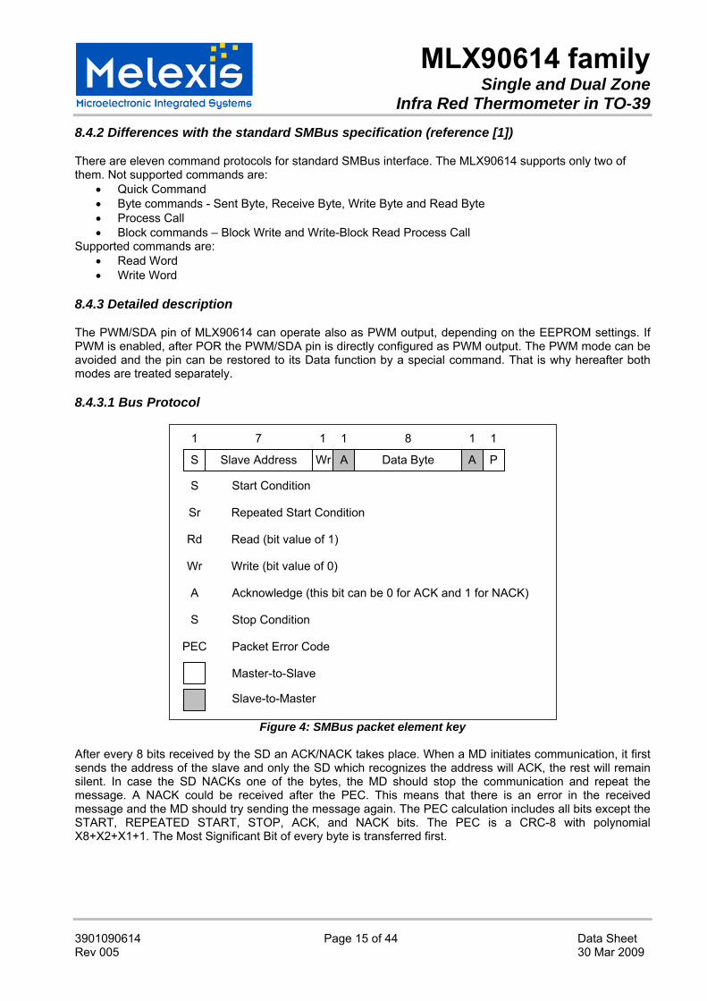
8.4.3.1 Bus Protocol
Figure 4: SMBus packet element key
After every 8 bits received by the SD an ACK/NACK takes place. When a MD initiates communication, it first sends the address of the slave and only the SD which recognizes the address will ACK, the rest will remain silent. In case the SD NACKs one of the bytes, the MD should stop the communication and repeat the message. A NACK could be received after the PEC. This means that there is an error in the received message and the MD should try sending the message again. The PEC calculation includes all bits except the START, REPEATED START, STOP, ACK, and NACK bits. The PEC is a CRC-8 with polynomial X8+X2+X1+1. The Most Significant Bit of every byte is transferred first.
S WrSlave Address A Data Byte A P
S Start Condition
Sr Repeated Start Condition
Rd Read (bit value of 1)
Wr Write (bit value of 0)
A Acknowledge (this bit can be 0 for ACK and 1 for NACK)
S Stop Condition
PEC Packet Error Code
Master-to-Slave
Slave-to-Master
1 17 1 8 1 1

MLX90614 family Single and Dual Zone
Infra Red Thermometer in TO-39
3901090614 Page 16 of 44 Data Sheet Rev 005 30 Mar 2009
8.4.3.1.1 Read Word (depending on the command – RAM or EEPROM)
Figure 5: SMBus read word format
8.4.3.1.2 Write Word (depending on the command – RAM or EEPROM)
Figure 6: SMBus write word format
Figure 7: SMbus communication examples (Read RAM and Write EEPROM)
S Wr Slave Address A
Data Byte Low A P
Command A Sr Slave Address Rd
1 7 1 1 8 1 1 7 1
8 1 1
………..
………..
A
1
Data Byte High A
8 1
PEC A
8 1
S WrSlave Address A
Data Byte Low A P
Command A
1 7 1 1 8 1
8 1 1
………..
……….. Data Byte High A
8 1
PEC A
8 1
MLX90614 family Single and Dual Zone
Infra Red Thermometer in TO-39
3901090614 Page 17 of 44 Data Sheet Rev 005 30 Mar 2009
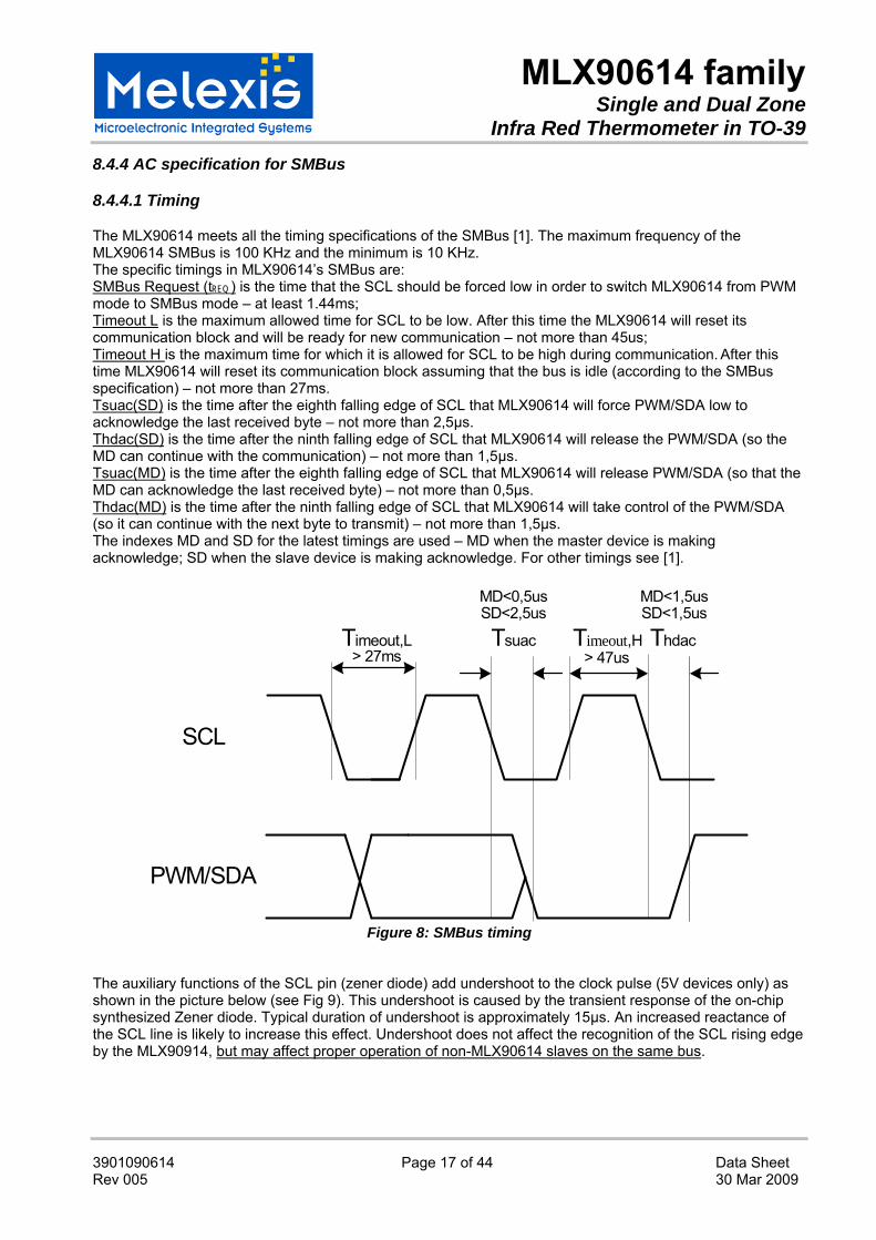
8.4.4 AC specification for SMBus
8.4.4.1 Timing
The MLX90614 meets all the timing specifications of the SMBus [1]. The maximum frequency of the MLX90614 SMBus is 100 KHz and the minimum is 10 KHz. The specific timings in MLX90614’s SMBus are: SMBus Request (tREQ ) is the time that the SCL should be forced low in order to switch MLX90614 from PWM mode to SMBus mode – at least 1.44ms; Timeout L is the maximum allowed time for SCL to be low. After this time the MLX90614 will reset its communication block and will be ready for new communication – not more than 45us; Timeout H is the maximum time for which it is allowed for SCL to be high during communication. After this time MLX90614 will reset its communication block assuming that the bus is idle (according to the SMBus specification) – not more than 27ms. Tsuac(SD) is the time after the eighth falling edge of SCL that MLX90614 will force PWM/SDA low to acknowledge the last received byte – not more than 2,5μs. Thdac(SD) is the time after the ninth falling edge of SCL that MLX90614 will release the PWM/SDA (so the MD can continue with the communication) – not more than 1,5μs. Tsuac(MD) is the time after the eighth falling edge of SCL that MLX90614 will release PWM/SDA (so that the MD can acknowledge the last received byte) – not more than 0,5μs. Thdac(MD) is the time after the ninth falling edge of SCL that MLX90614 will take control of the PWM/SDA (so it can continue with the next byte to transmit) – not more than 1,5μs. The indexes MD and SD for the latest timings are used – MD when the master device is making acknowledge; SD when the slave device is making acknowledge. For other timings see [1].
PWM/SDA
SCL
Tsuac ThdacTimeout,L Timeout,H> 27ms > 47us
SD<2,5usMD<0,5us
SD<1,5usMD<1,5us
Figure 8: SMBus timing
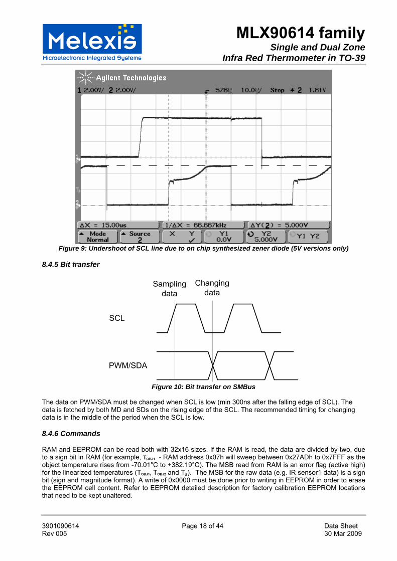
The auxiliary functions of the SCL pin (zener diode) add undershoot to the clock pulse (5V devices only) as shown in the picture below (see Fig 9). This undershoot is caused by the transient response of the on-chip synthesized Zener diode. Typical duration of undershoot is approximately 15μs. An increased reactance of the SCL line is likely to increase this effect. Undershoot does not affect the recognition of the SCL rising edge by the MLX90914, but may affect proper operation of non-MLX90614 slaves on the same bus.
MLX90614 family Single and Dual Zone
Infra Red Thermometer in TO-39
3901090614 Page 18 of 44 Data Sheet Rev 005 30 Mar 2009
Figure 9: Undershoot of SCL line due to on chip synthesized zener diode (5V versions only)
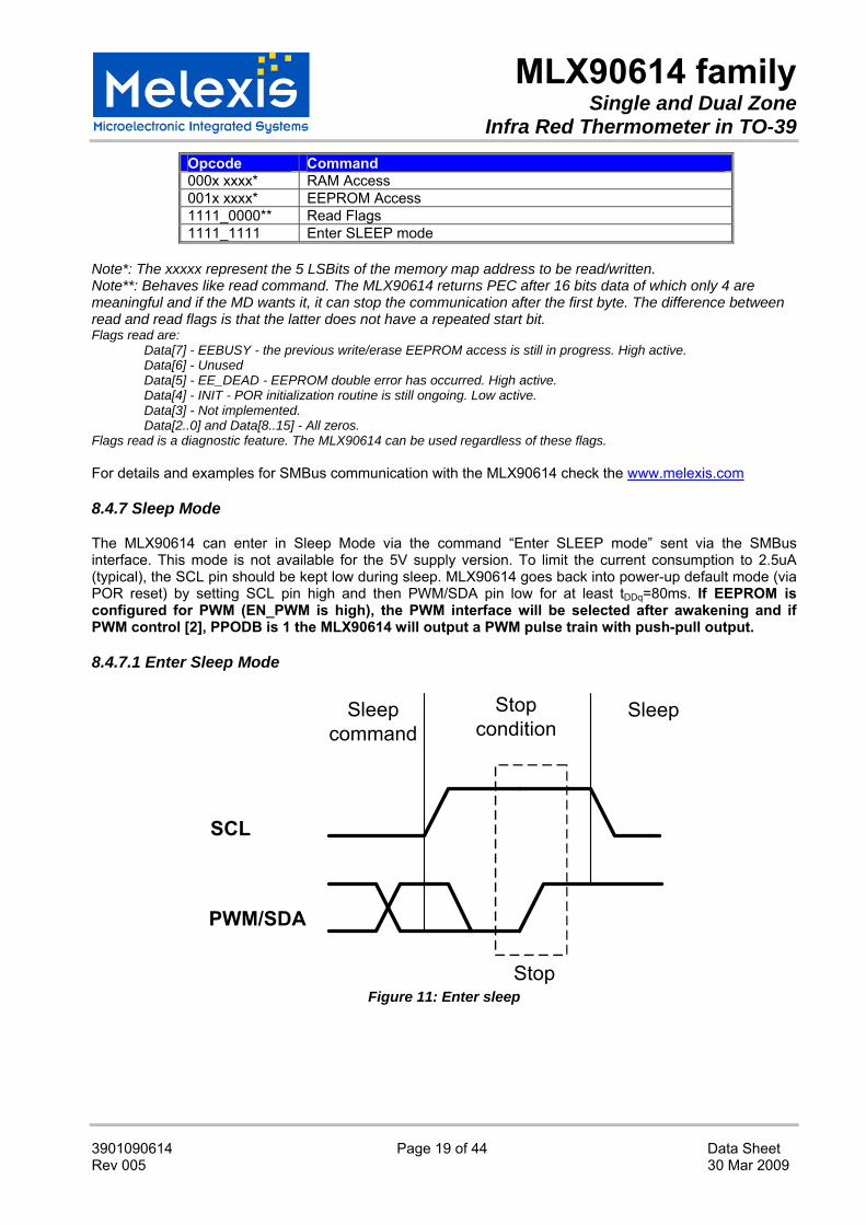
8.4.5 Bit transfer
PWM/SDA
SCL
Samplingdata
Changingdata
Figure 10: Bit transfer on SMBus
The data on PWM/SDA must be changed when SCL is low (min 300ns after the falling edge of SCL). The data is fetched by both MD and SDs on the rising edge of the SCL. The recommended timing for changing data is in the middle of the period when the SCL is low.
8.4.6 Commands
RAM and EEPROM can be read both with 32x16 sizes. If the RAM is read, the data are divided by two, due to a sign bit in RAM (for example, TOBJ1 - RAM address 0x07h will sweep between 0x27ADh to 0x7FFF as the object temperature rises from -70.01°C to +382.19°C). The MSB read from RAM is an error flag (active high) for the linearized temperatures (TOBJ1, TOBJ2 and Ta). The MSB for the raw data (e.g. IR sensor1 data) is a sign bit (sign and magnitude format). A write of 0x0000 must be done prior to writing in EEPROM in order to erase the EEPROM cell content. Refer to EEPROM detailed description for factory calibration EEPROM locations that need to be kept unaltered.
MLX90614 family Single and Dual Zone
Infra Red Thermometer in TO-39
3901090614 Page 19 of 44 Data Sheet Rev 005 30 Mar 2009
Opcode Command 000x xxxx* RAM Access 001x xxxx* EEPROM Access 1111_0000** Read Flags 1111_1111 Enter SLEEP mode
Note*: The xxxxx represent the 5 LSBits of the memory map address to be read/written. Note**: Behaves like read command. The MLX90614 returns PEC after 16 bits data of which only 4 are meaningful and if the MD wants it, it can stop the communication after the first byte. The difference between read and read flags is that the latter does not have a repeated start bit. Flags read are:
Data[7] - EEBUSY - the previous write/erase EEPROM access is still in progress. High active. Data[6] - Unused Data[5] - EE_DEAD - EEPROM double error has occurred. High active. Data[4] - INIT - POR initialization routine is still ongoing. Low active. Data[3] - Not implemented. Data[2..0] and Data[8..15] - All zeros.
Flags read is a diagnostic feature. The MLX90614 can be used regardless of these flags. For details and examples for SMBus communication with the MLX90614 check the www.melexis.com
8.4.7 Sleep Mode
The MLX90614 can enter in Sleep Mode via the command “Enter SLEEP mode” sent via the SMBus interface. This mode is not available for the 5V supply version. To limit the current consumption to 2.5uA (typical), the SCL pin should be kept low during sleep. MLX90614 goes back into power-up default mode (via POR reset) by setting SCL pin high and then PWM/SDA pin low for at least tDDq=80ms. If EEPROM is configured for PWM (EN_PWM is high), the PWM interface will be selected after awakening and if PWM control [2], PPODB is 1 the MLX90614 will output a PWM pulse train with push-pull output.
8.4.7.1 Enter Sleep Mode
Sleepcommand
Stopcondition
Stop
Sleep
SCL
PWM/SDA
Figure 11: Enter sleep

MLX90614 family Single and Dual Zone
Infra Red Thermometer in TO-39
3901090614 Page 20 of 44 Data Sheet Rev 005 30 Mar 2009
8.4.7.2 Exit from Sleep Mode
Sleep Awake
SCL
PWM/SDA
twake
> 33ms
Figure 12: Exit Sleep Mode
First data is available 0.25 seconds (typ) after exit from Sleep is done. On-chip IIR filter is skipped for the very first measurement. All measurements afterwards pass the embedded digital filtering as configured in EEPROM. Details on embedded filtering are available in application note “Understanding MLX90614 on-chip digital signal filters”, available from www.melexis.com SCL line is kept low in order to reduce current leakage trough the pin (artificial zener diode is connected to that pin).
8.5 PWM
The MLX90614 can be read via PWM or SMBus compatible interface. Selection of PWM output is done in EEPROM configuration (factory default is SMBus). PWM output has two programmable formats, single and dual data transmission, providing single wire reading of two temperatures (dual zone object or object and ambient). The PWM period is derived from the on-chip oscillator and is programmable.
Config Register[5:4] PWM1 data PWM2 data Tmin,1 Tmax,1 Tmin,2 Tmax,2 00 Ta Tobj1 Tarange,L Tarange,H Tomin Tomax 01 Ta Tobj2 Tarange,L Tarange,H Tomin Tomax 11 Tobj1 Tobj2 Tomin Tomax Tomin Tomax 10* Tobj2 Undefined Tomin Tomax N.A. N.A.
Note: Serial data functions (2-wire / PWM) are multiplexed with a thermal relay function (described in the “Thermal relay” section). * not recommended for extended PWM format operation

MLX90614 family Single and Dual Zone
Infra Red Thermometer in TO-39
3901090614 Page 21 of 44 Data Sheet Rev 005 30 Mar 2009
t1 t2
t3
t4
OV
F
UN
F
FE
Valid data band
Error band
Start Stop
0 T58T1
8 T1116 T12
16 T1316 T7
8 T
t1 t2
t3
t4
OV
FU
NF
FESensor 1
Error band
Start Stop
0 T116 TT5
16 T716 T8
16
Valid data band
t5 t6
Sensor 1
t7
OV
FU
NF
FE
Error bandSensor 2
Sensor 2Valid data band
t8
T916 T13
16 T1516
Figure 13: PWM timing single (above) and extended PWM (bellow)
PWM type t1 t2 t3 t4 t5 t6 t7 t8
Single 1/8 – high 4/8 - var 2/8 1/8 – low NA NA NA NA Extended - S1 1/16 - high 4/16 - var 2/16 1/16 - low 1/16 - low 4/16 - low 2/16 - low 1/16 - low
Extended - S2 1/16 - high 4/16 - high 2/16 - high 1/16 - high 1/16 - high 4/16 - var 2/16 1/16 - low
8.5.1 Single PWM format
In single PWM output mode the settings for PWM1 data only are used. The temperature reading can be calculated from the signal timing as:
( ) TminTminTmaxTtTout +⎥⎦
⎤⎢⎣⎡ −= 22
,
where Tmin and Tmax are the corresponding rescale coefficients in EEPROM for the selected temperature output (Ta, object temperature range is valid for both Tobj1 and Tobj2 as specified in the previous table) and T is the PWM period. Tout is Tobj1, Tobj2 or Ta according to Config Register [5:4] settings.

MLX90614 family Single and Dual Zone
Infra Red Thermometer in TO-39
3901090614 Page 22 of 44 Data Sheet Rev 005 30 Mar 2009
The different time intervals t1…t4 have following meaning: t1: Start buffer. During this time the signal is always high. t1 = 0.125*T (T is the PWM period, refer to fig. 13). t2: Valid Data Output Band, 0…1/2T. PWM output data resolution is 10 bit. t3: Error band – information for fatal error in EEPROM (double error detected, not correctable). t3 = 0.25 * T. Therefore a PWM pulse train with a duty cycle of 0.875 will indicate a fatal error in EEPROM (for single PWM format). OVF means Overflow, UNF means Underflow and FE mean Fatal Error. Example: Tobj1 => Config Reg[5:4] = 11’b Tomin = 0°C => Tomin [EEPROM] = 100 * (tomin + 273.15) = 6AB3h Tomax = +50°C => Tomax [EEPROM] = 100 * (tomax + 273.15) = 7E3Bh Captured PWM high duration is 0.495*T => t2=(0.495 – 0.125)*T=0.370*T => measured object temperature = 2X0.370* (50°C -0°C)+0°C = +37.0°C.
8.5.2 Extended PWM format
The PWM format for extended PWM is shown in Figure 13. Note that with bits DUAL[5:1]>00h each period will be outputted 2N+1 times, where N is the decimal value of the number written in DUAL[5:1] (DUAL[5:1] =PWM control & clock [8:4] ), like shown on Figure 14.
Figure 14: Extended PWM format with DUAL [5:1] = 01h (2 repetitions for each data)
The temperature transmitted in Data 1 field can be calculated using the following equation:
( ) 1112
1 *2 TminTminTmaxTtTout +⎥⎦
⎤⎢⎣⎡ −=
For Data 2 field the equation is:
( ) 2225
2 *2 TminTminTmaxTtTout +⎥⎦
⎤⎢⎣⎡ −=
Where Tmin1, Tmax1, Tmin2 and Tmax2 are given in Table 9, t2=thigh1-t1, and t5=thigh2-t4. Time bands are: t1=0.125*T, t3=0.25*T and t4=1.125*T. As shown in Figure 11, in extended PWM format the period is twice the period for the single PWM format. All equations provided herein are given for the single PWM period T. The EEPROM Error band signaling will be 43.75% duty cycle for Data1 and 93.75% for Data2. Note: EEPROM error signaling is implemented in automotive grade parts only. Example: Configuration: Ta : Tobj1 @ Data1 : Data2 => Config Reg[5:4] = 00b, Tamin = -5°C => Tarange, L [EEPROM] = 100*(Tamin+38.2)/64 = 34h, Tamax = +105°C => Tarange,H [EEPROM] = 100*(Tamax+38.2)/64 = E0h,
Tarange [EEPROM]=E034h Tomin = 0°C => Tomin [EEPROM] = 100 * (Tomin + 273.15) = 6AB3h Tomax = +50°C => Tomax [EEPROM] = 100 * (Tomax + 273.15) = 7E3Bh Captured high durations are 0.13068*(2T) and 0.7475*(2T), where 2T is each captured PWM period. Time band t4 is provided for reliable determination between Data1 and Data2 data fields. Thus Data1 is represented by 0.13068*(2T) and Data2 – by 0.7475*(2T), and the temperatures can be calculated as follows: t2/T=(thigh1/T)-0.125=0.13636 => Ta=+25.0°C, t5/T=( thigh2/T)-1.125=0.370 => Tobj1=+37.0°C.

MLX90614 family Single and Dual Zone
Infra Red Thermometer in TO-39
3901090614 Page 23 of 44 Data Sheet Rev 005 30 Mar 2009
8.5.3 Customizing the temperature range for PWM output
The calculated ambient and object temperatures are stored in RAM with a resolution of 0.01 °C (16 bit). The PWM operates with a 10-bit word so the transmitted temperature is rescaled in order to fit in the desired range. For this goal 2 cells in EEPROM are foreseen to store the desired range for To (Tomin and Tomax) and one for Ta (Tarange: the 8MSB are foreseen for Tamax and the 8LSB for Tamin). Thus the output range for To can be programmed with an accuracy of 0.01 °C, while the corresponding Ta range can be programmed with an accuracy of 0.64 °C. The object data for PWM is rescaled according to the following equation:
1023, EEPROMEEPROMEEPROM
obj
MINMAXobjPWM
objPWM
MINRAMPWM
TTK
KTT
T−
=−
=
The TRAM is the linearized Tobj, 16-bit (0000…FFFFh, 0000 for -273.15°C and FFFFh for +382.2°C) and the result is a 10-bit word, in which 000h corresponds to ToMIN[°C], 3FFh corresponds to ToMAX[°C] and 1LSB
corresponds to 1023
MINMAX ToTo −[°C]
100∗= MINMIN TTEEPORM
LSB
100∗= MAXMAX TTEEPORM
LSB The ambient data for PWM is rescaled according to the following equation:
1023, EEPROMEEPROM
ambient
EEPROM
ambient
MINMAXambientPWM
PWM
MINRAMPWM
TTK
KTT
T−
=−
=
The result is a 10-bit word, where 000h corresponds to -38.2 °C (lowest Ta that can be read via PWM), 3FFh
corresponds to 125 °C (highest Ta that can be read via PWM) and 1LSB corresponds to 1023
MINMAX TT −[°C]
( )[ ]64
1002.38 ∗−−= MINMIN TTEEPORM
LSB
( )[ ]64
1002.38 ∗−−= MAXMAX TTEEPORM
LSB
MLX90614 family Single and Dual Zone
Infra Red Thermometer in TO-39
3901090614 Page 24 of 44 Data Sheet Rev 005 30 Mar 2009
8.6 Switching Between PWM and SMBus communication
8.6.1 PWM is enabled
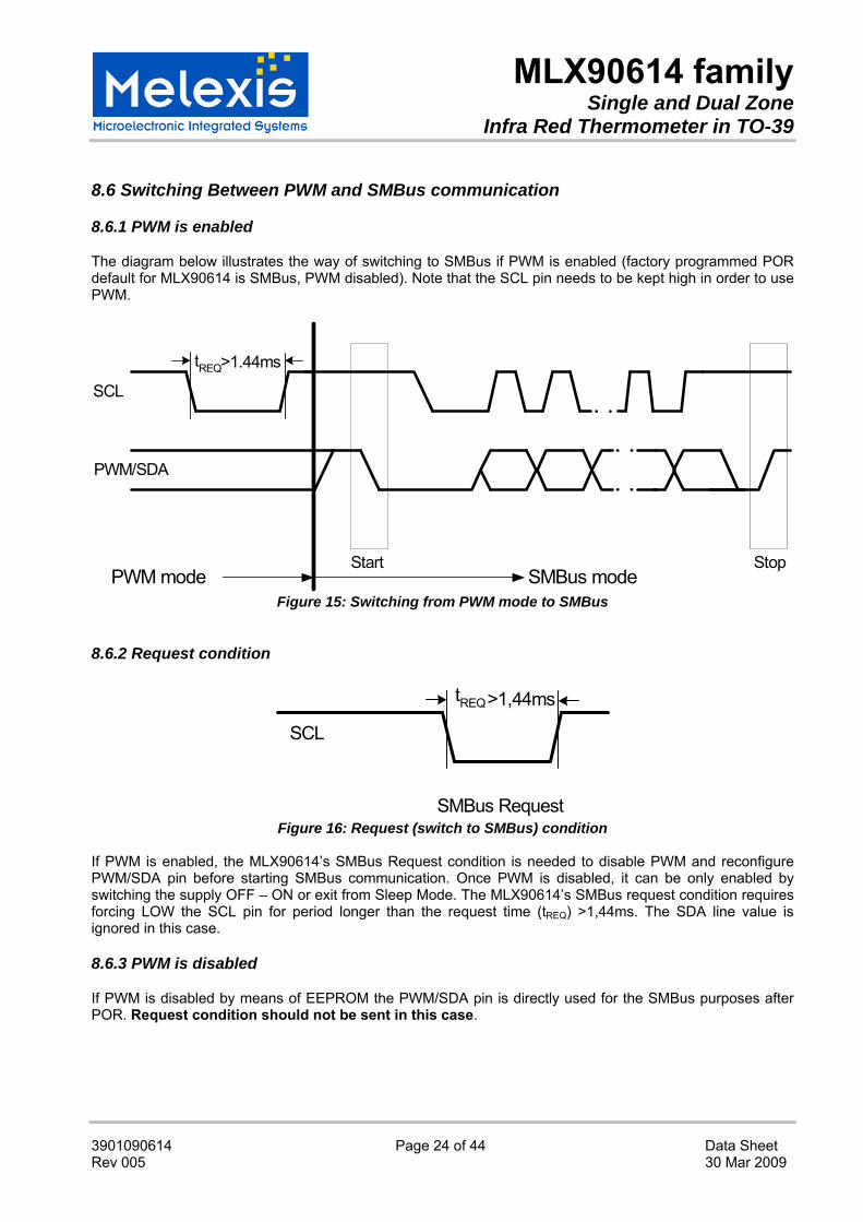
The diagram below illustrates the way of switching to SMBus if PWM is enabled (factory programmed POR default for MLX90614 is SMBus, PWM disabled). Note that the SCL pin needs to be kept high in order to use PWM.
SCL
PWM/SDA
Start Stop
tREQ
PWM mode SMBus mode
>1.44ms
Figure 15: Switching from PWM mode to SMBus
8.6.2 Request condition
SCL
SMBus Request
tREQ>1,44ms
Figure 16: Request (switch to SMBus) condition
If PWM is enabled, the MLX90614’s SMBus Request condition is needed to disable PWM and reconfigure PWM/SDA pin before starting SMBus communication. Once PWM is disabled, it can be only enabled by switching the supply OFF – ON or exit from Sleep Mode. The MLX90614’s SMBus request condition requires forcing LOW the SCL pin for period longer than the request time (tREQ) >1,44ms. The SDA line value is ignored in this case.
8.6.3 PWM is disabled
If PWM is disabled by means of EEPROM the PWM/SDA pin is directly used for the SMBus purposes after POR. Request condition should not be sent in this case.
MLX90614 family Single and Dual Zone
Infra Red Thermometer in TO-39
3901090614 Page 25 of 44 Data Sheet Rev 005 30 Mar 2009
8.7 Computation of ambient and object temperatures
The IR sensor consists of serial connected thermo-couples with cold junctions placed at thick chip substrate and hot junctions, placed over thin membrane. The IR radiation absorbed from the membrane heats (or cools) it. The thermopile output signal is:
( ) ( )44., TaToAToTaVir −= ,
Where To is the object temperature absolute (Kelvin) temperature, Ta is the sensor die absolute (Kelvin) temperature, and A is the overall sensitivity. An on board temperature sensor is needed to measure the chip temperature. After measurement of the output of both sensors, the corresponding ambient and object temperatures can be calculated. These calculations are done by the internal DSP, which produces digital outputs, linearly proportional to measured temperatures.
8.7.1 Ambient temperature Ta
The Sensor die temperature is measured with a PTC or a PTAT element. All the sensors conditioning and data processing is handled on-chip and the linearized sensor die temperature Ta is made available in memory. The resolution of the calculated temperature is 0.02 ˚C. The sensor is factory calibrated for the full automotive range (-40…+125 ˚C). In RAM cell 006h, 2DE4h corresponds to -38.2 ˚C (linearization output lower limit) and 4DC4h (19908d) corresponds to 125 ˚C. The conversions from RAM contend to real Ta is easy using the following relation:
02.0][ ×=° TaregKTa , or 0.02 °K / LSB.
8.7.2 Object temperature To
The result has a resolution of 0.02 ˚C and is available in RAM. To is derived from RAM as:
02.0][ ×=° ToregKTo , or 0.02 °K / LSB. Please note that 1LSB corresponds to 0,02Deg and the MSB bit is error flag (if “1” then error).
Example: 1. 0000 => -273,15˚C (no error) - min possible value returned by MLX90614 2. 0001 => -273.13˚C (no error) 3. 0002 => -273,11˚C (no error) and so on 4. 3AF7 => 28,75˚C (no error) 5. 7FFF => 382,19˚C (no error) - max possible value returned by MLX90614 The result is calculated by following expressions: 1. Convert it to decimal value i.e 3AF7h = 15095d 2. Divide by 50 (or multiply by 0,02) i.e. 15095/50=301,9K (result is in Kelvin) 3. Convert K -> ˚C i.e. 301,9-273,15=28,75˚C
8.7.3 Calculation flow
The measurement, calculation and linearization are held by core, which executes a program form ROM. After POR the chip is initialized with calibration data from EEPROM. During this phase the number of IR sensors is selected and it is decided which temperature sensor will be used. Measurements, compensation and linearization routines run in a closed loop afterwards.
MLX90614 family Single and Dual Zone
Infra Red Thermometer in TO-39
3901090614 Page 26 of 44 Data Sheet Rev 005 30 Mar 2009
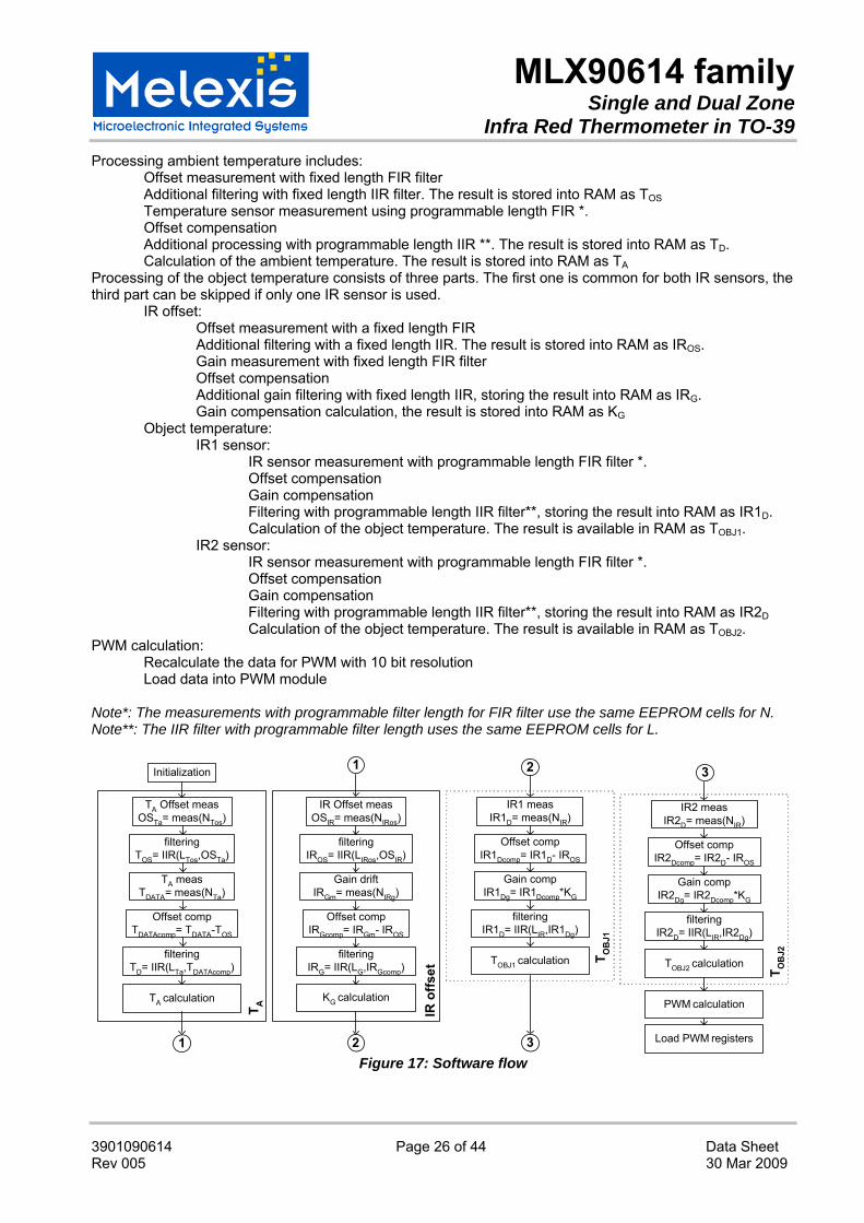
Processing ambient temperature includes: Offset measurement with fixed length FIR filter Additional filtering with fixed length IIR filter. The result is stored into RAM as TOS Temperature sensor measurement using programmable length FIR *. Offset compensation Additional processing with programmable length IIR **. The result is stored into RAM as TD. Calculation of the ambient temperature. The result is stored into RAM as TA Processing of the object temperature consists of three parts. The first one is common for both IR sensors, the third part can be skipped if only one IR sensor is used. IR offset: Offset measurement with a fixed length FIR Additional filtering with a fixed length IIR. The result is stored into RAM as IROS. Gain measurement with fixed length FIR filter Offset compensation Additional gain filtering with fixed length IIR, storing the result into RAM as IRG. Gain compensation calculation, the result is stored into RAM as KG Object temperature: IR1 sensor: IR sensor measurement with programmable length FIR filter *. Offset compensation Gain compensation Filtering with programmable length IIR filter**, storing the result into RAM as IR1D. Calculation of the object temperature. The result is available in RAM as TOBJ1.
IR2 sensor: IR sensor measurement with programmable length FIR filter *. Offset compensation Gain compensation Filtering with programmable length IIR filter**, storing the result into RAM as IR2D Calculation of the object temperature. The result is available in RAM as TOBJ2. PWM calculation: Recalculate the data for PWM with 10 bit resolution Load data into PWM module Note*: The measurements with programmable filter length for FIR filter use the same EEPROM cells for N. Note**: The IIR filter with programmable filter length uses the same EEPROM cells for L.
Initialization
TA Offset measOSTa= meas(NTos)
filteringTOS= IIR(LTos,OSTa)
TA measTDATA= meas(NTa)
Offset compTDATAcomp= TDATA-TOS
filteringTD= IIR(LTa,TDATAcomp)
TA calculation
T A
IR Offset measOSIR= meas(NIRos)
filteringIROS= IIR(LIRos,OSIR)
IR1 measIR1D= meas(NIR)
Offset compIR1Dcomp= IR1D- IROS
filteringIR1D= IIR(LIR,IR1Dg)
TOBJ1 calculation
Gain driftIRGm= meas(NIRg)
Offset compIRGcomp= IRGm- IROS
filteringIRG= IIR(LG,IRGcomp)
KG calculation
IR o
ffset
Gain compIR1Dg= IR1Dcomp*KG
IR2 measIR2D= meas(NIR)
Offset compIR2Dcomp= IR2D- IROS
filteringIR2D= IIR(LIR,IR2Dg)
TOBJ2 calculation
Gain compIR2Dg= IR2Dcomp*KG
T OB
J1
T OB
J2
PWM calculation
Load PWM registers1
1 2 3
2 3 Figure 17: Software flow

MLX90614 family Single and Dual Zone
Infra Red Thermometer in TO-39
3901090614 Page 27 of 44 Data Sheet Rev 005 30 Mar 2009
8.8 Thermal relay
The MLX90614 can be configured to behave as a thermo relay with programmable threshold and hysteresis on the PWM/SDA pin. The input for the comparator unit of the relay is the object temperature from sensor 1 The output of the MLX90614 is NOT a relay driver but a logical output which should be connected to a relay driver if necessary. The output driver is one and the same for PWM and Thermal relay. In order to configure the MLX90614 to work as thermal relay two conditions must be met:
o Set bit TRPWMB high at address 002h in EEPROM o Enable PWM output i.e. EN_PWM is set high
The PWM/SDA pin can be programmed as a push-pull or open drain NMOS (via bit PPODB in EEPROM PWMCTRL), which can trigger an external device. The temperature threshold data is determined by EEPROM at address 021h (Tomin) and the hysteresis at address 020h (Tomax). The logical state of the PWM/SDA pin is as follows:
PWM/SDA pin is high if hysteresisthresholdTobj +≥1
PWM/SDA pin is low if hysteresisthresholdTobj −≤1
threshold
hysteresis hysteresis
T
“0”
“1”
Figure 18: Thermal relay : “PWM” pin versus Tobj
The MLX90614 preserves its normal operation when configured as a thermal relay (PWM configuration and specification applies as a general rule also for the thermal relay) and therefore it can be read using the SMBus (entering the SMBus mode from both PWM and thermal relay configuration is the same). For example, the MLX90614 can generate a wake-up alert for a system upon reaching a certain temperature and then be read as a thermometer. A reset condition (enter-and exit Sleep, for example) will be needed in order to return to the thermal relay configuration. Example: threshold 5 °C => (5 + 273.15)*100 = 27815 = 6CA7h hysteresis is 1°C => 1 * 100 = 100 = 64h (smallest possible hysteresis is 0,01°C or 1h) PWM/SDA pin will be low at object temperature below 4 °C PWM/SDA pin will be high at object temperature higher that 6 °C
MLX90614 family Single and Dual Zone
Infra Red Thermometer in TO-39
3901090614 Page 28 of 44 Data Sheet Rev 005 30 Mar 2009
9 Unique Features
The MLX90614 is a ready-to use low-cost non contact thermometer provided from Melexis with output data linearly dependent on the object temperature with high accuracy and extended resolution. It supports versatile customization to a very wide range of temperatures, power supplies and refresh rates. The user can program the internal object emissivity correction for objects with a low emissivity. An embedded error checking and correction mechanism provides high memory reliability. The sensors are housed in an industry standard TO39 package for both single- and dual-zone IR thermometers. The thermometer is available in automotive grade and can use two different packages for wider applications’ coverage. The low power consumption and sleep mode make the thermometer ideally suited for handheld mobile applications. The digital sensor interface can be either a power-up-and-measure PWM or an enhanced access SMBus compatible protocol. Systems with more than 100 devices can be built with only two signal lines. Dual zone non contact temperature measurements are available via a single line (extended PWM). A built-in thermal relay function further extends the easy implementation of wide variety of freezing/boiling prevention and alert systems, as well as thermostats (no MCU is needed).

MLX90614 family Single and Dual Zone
Infra Red Thermometer in TO-39
3901090614 Page 29 of 44 Data Sheet Rev 005 30 Mar 2009
10 Performance Graphs
10.1 Temperature accuracy of the MLX90614
All accuracy specifications apply under settled isothermal conditions only. Furthermore, the accuracy is only valid if the object fills the FOV of the sensor completely.
-70
-20 0Ta,oC
50 100 125-40
-40
0
60
120
180
240
300
380To,oC
± 1 oC
± 1 oC
± 1 oC
± 1 oC
± 2 oC
± 3 oC
± 2 oC ± 2 oC
± 3 oC
± 3 oC
± 2 oC± 3 oC
± 3 oC ± 4 oC
± 4 oC
± 4 oC ± 3 oC
± 4 oC
± 3 oC± 2 oC
± 1 oC
± 1 oC ± 2 oC
± 2 oC
± 2 oC± 2 oC
± 3 oC
± 0.5 oC
Figure 19: Preliminary accuracy of MLX90614 (Ta,To)
MLX90614 family Single and Dual Zone
Infra Red Thermometer in TO-39
3901090614 Page 30 of 44 Data Sheet Rev 005 30 Mar 2009
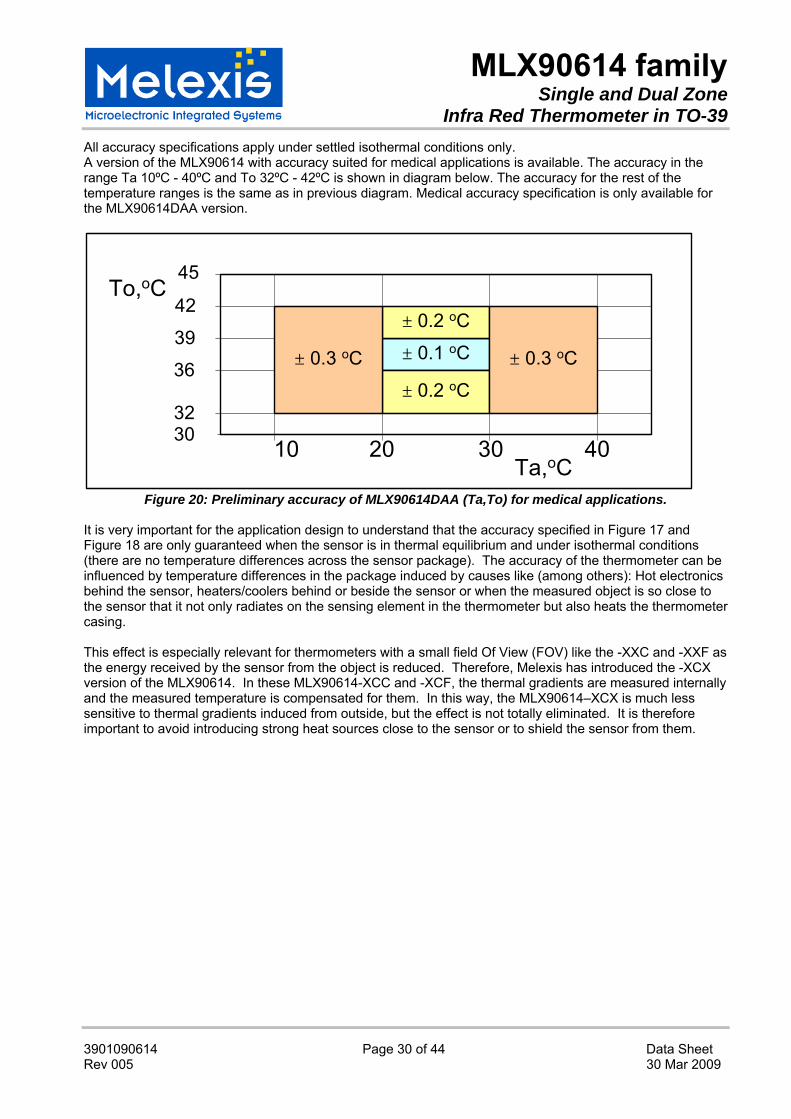
All accuracy specifications apply under settled isothermal conditions only. A version of the MLX90614 with accuracy suited for medical applications is available. The accuracy in the range Ta 10ºC - 40ºC and To 32ºC - 42ºC is shown in diagram below. The accuracy for the rest of the temperature ranges is the same as in previous diagram. Medical accuracy specification is only available for the MLX90614DAA version.
40302010
36
45
32
39
42
± 0.1 oC
± 0.2 oC
± 0.2 oC
± 0.3 oC ± 0.3 oC
30
Ta,oC
To,oC
Figure 20: Preliminary accuracy of MLX90614DAA (Ta,To) for medical applications.
It is very important for the application design to understand that the accuracy specified in Figure 17 and Figure 18 are only guaranteed when the sensor is in thermal equilibrium and under isothermal conditions (there are no temperature differences across the sensor package). The accuracy of the thermometer can be influenced by temperature differences in the package induced by causes like (among others): Hot electronics behind the sensor, heaters/coolers behind or beside the sensor or when the measured object is so close to the sensor that it not only radiates on the sensing element in the thermometer but also heats the thermometer casing. This effect is especially relevant for thermometers with a small field Of View (FOV) like the -XXC and -XXF as the energy received by the sensor from the object is reduced. Therefore, Melexis has introduced the -XCX version of the MLX90614. In these MLX90614-XCC and -XCF, the thermal gradients are measured internally and the measured temperature is compensated for them. In this way, the MLX90614–XCX is much less sensitive to thermal gradients induced from outside, but the effect is not totally eliminated. It is therefore important to avoid introducing strong heat sources close to the sensor or to shield the sensor from them.

MLX90614 family Single and Dual Zone
Infra Red Thermometer in TO-39
3901090614 Page 31 of 44 Data Sheet Rev 005 30 Mar 2009
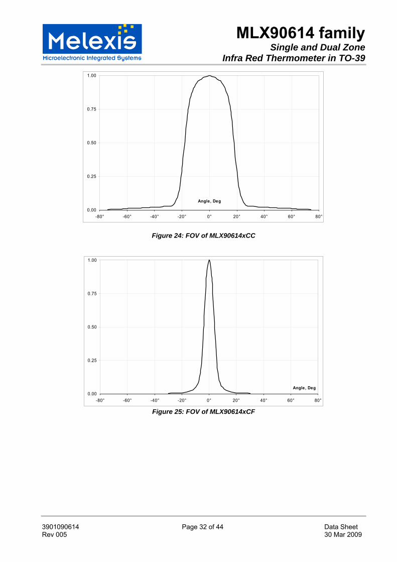
10.2 Field Of View (FOV)
Field of view is determined at 50% thermopile signal and with respect to the sensor main axis.
Parameter MLX90614xAA MLX90614xBA MLX90614xCC MLX90614xCF
Peak zone 1 ±0° -25° ±0° ±0°
Width zone 1 90° 70° 35° 10
Peak zone 2 -25°
Width zone 2 Not applicable
70° Not applicable Not applicable
0.00
0.25
0.50
0.75
1.00
-80° -60° -40° -20° 0° 20° 40° 60° 80°
Angle, Deg
Figure 19: FOV of MLX90614xAA
0.00
0.25
0.50
0.75
1.00
-80° -60° -40° -20° 0° 20° 40° 60° 80°
Angle, Deg
Figure 22: FOV of MLX90614xBA
Figure 23: identification of zone 1&2 relative to alignment tab.
MLX90614 family Single and Dual Zone
Infra Red Thermometer in TO-39
3901090614 Page 32 of 44 Data Sheet Rev 005 30 Mar 2009
0.00
0.25
0.50
0.75
1.00
-80° -60° -40° -20° 0° 20° 40° 60° 80°
Angle, Deg
Figure 24: FOV of MLX90614xCC
0.00
0.25
0.50
0.75
1.00
-80° -60° -40° -20° 0° 20° 40° 60° 80°
Angle, Deg
Figure 25: FOV of MLX90614xCF
MLX90614 family Single and Dual Zone
Infra Red Thermometer in TO-39
3901090614 Page 33 of 44 Data Sheet Rev 005 30 Mar 2009
11 Applications Information
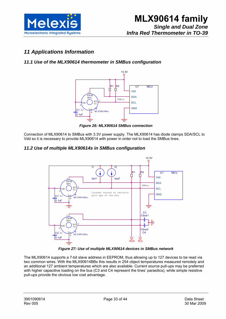
11.1 Use of the MLX90614 thermometer in SMBus configuration
SCLVzVdd
R2
2
C1
0.1uF
3
U1 MCU
SCL
SDA
GND
Vdd
4
+3.3V
PW MSDA
U2 MLX90614Bxx
R1
1 SMBus
Vss
Figure 26: MLX90614 SMBus connection
Connection of MLX90614 to SMBus with 3.3V power supply. The MLX90614 has diode clamps SDA/SCL to Vdd so it is necessary to provide MLX90614 with power in order not to load the SMBus lines.
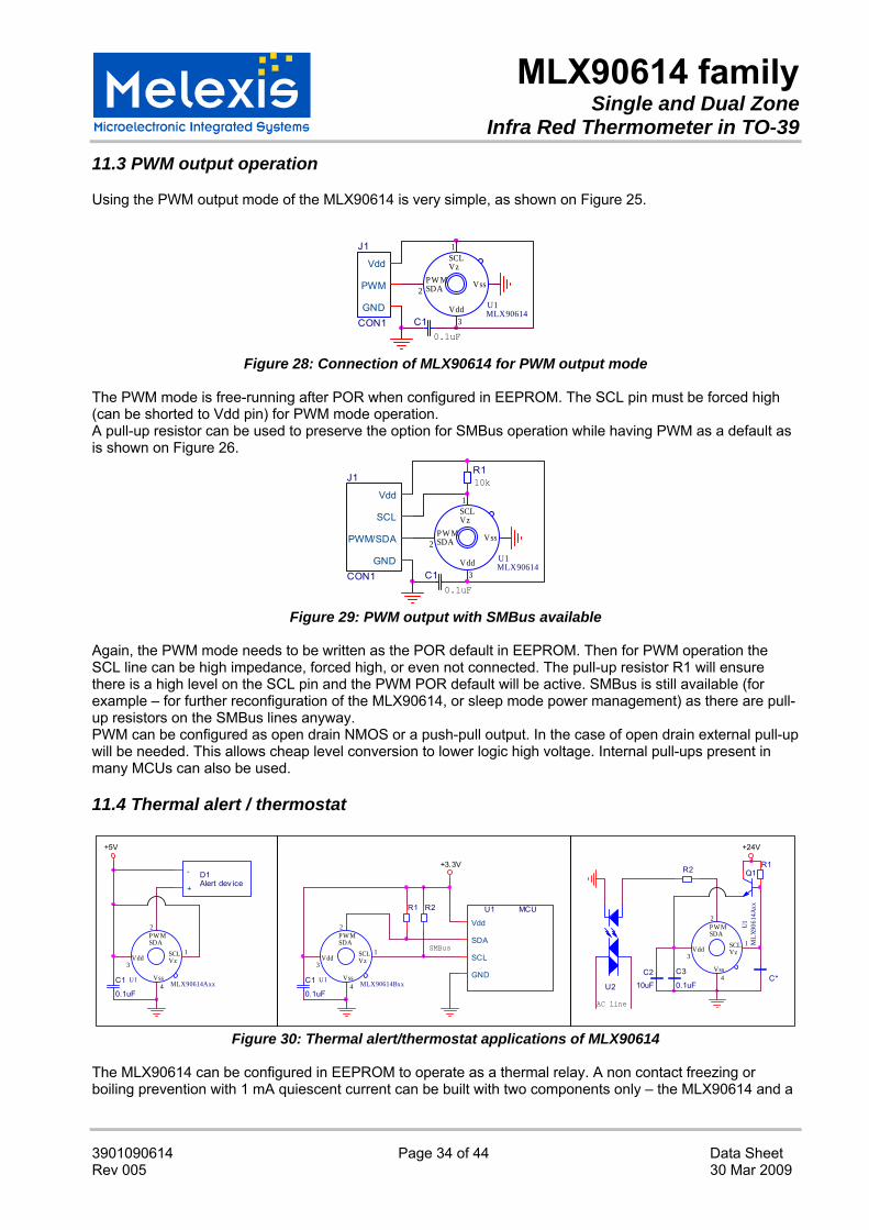
11.2 Use of multiple MLX90614s in SMBus configuration
R2
U1 MLX90614Bxx4
1
2
SCLVz
U1 MLX90614Bxx
C4Cbus2
U1 MCU
SCL
SDA
GND
Vdd
1
I1
Ipu1
C2
0.1uF
SCLVz3
SDA
C3Cbus1
R1
3
SCL
4C1
0.1uF
Vss
+3.3V
I2
Ipu2
Vdd
Vdd
2
SMBus
VssCurrent source or resistorpull-ups of the bus
PW MSDA
PW MSDA
Figure 27: Use of multiple MLX90614 devices in SMBus network
The MLX90614 supports a 7-bit slave address in EEPROM, thus allowing up to 127 devices to be read via two common wires. With the MLX90614BBx this results in 254 object temperatures measured remotely and an additional 127 ambient temperatures which are also available. Current source pull-ups may be preferred with higher capacitive loading on the bus (C3 and C4 represent the lines’ parasitics), while simple resistive pull-ups provide the obvious low cost advantage.
MLX90614 family Single and Dual Zone
Infra Red Thermometer in TO-39
3901090614 Page 34 of 44 Data Sheet Rev 005 30 Mar 2009
11.3 PWM output operation
Using the PWM output mode of the MLX90614 is very simple, as shown on Figure 25.
J1
CON1
PWM
Vdd
GND
2
0.1uF
Vdd U1MLX90614
VssPW MSDA
1
C1
SCLVz
3
Figure 28: Connection of MLX90614 for PWM output mode
The PWM mode is free-running after POR when configured in EEPROM. The SCL pin must be forced high (can be shorted to Vdd pin) for PWM mode operation. A pull-up resistor can be used to preserve the option for SMBus operation while having PWM as a default as is shown on Figure 26.
PW MSDA
10k
3
1
Vdd
2
R1
SCLVz
J1
CON1
SCL
PWM/SDA
GND
Vdd
U1MLX90614
Vss
0.1uF
C1
Figure 29: PWM output with SMBus available
Again, the PWM mode needs to be written as the POR default in EEPROM. Then for PWM operation the SCL line can be high impedance, forced high, or even not connected. The pull-up resistor R1 will ensure there is a high level on the SCL pin and the PWM POR default will be active. SMBus is still available (for example – for further reconfiguration of the MLX90614, or sleep mode power management) as there are pull-up resistors on the SMBus lines anyway. PWM can be configured as open drain NMOS or a push-pull output. In the case of open drain external pull-up will be needed. This allows cheap level conversion to lower logic high voltage. Internal pull-ups present in many MCUs can also be used.
11.4 Thermal alert / thermostat
U2
AC line
R1
3C2
10uFC1
0.1uF
U1 MCU
SCL
SDA
GND
Vdd2
SCLVz
C*
2
SCLVz
U1M
LX90
614A
xx
U1 MLX90614BxxVss
Vdd1 1 SMBus
R2
Vdd
4
Q1
4
1
+5V
U1 MLX90614Axx
VddVss
+3.3V R1
C3
0.1uF
SCLVz3
R2
+24V
VssC1
0.1uF
PW MSDAPW M
SDA
3
4
PW MSDA
D1Alert dev ice
+
-
2
Figure 30: Thermal alert/thermostat applications of MLX90614
The MLX90614 can be configured in EEPROM to operate as a thermal relay. A non contact freezing or boiling prevention with 1 mA quiescent current can be built with two components only – the MLX90614 and a

MLX90614 family Single and Dual Zone
Infra Red Thermometer in TO-39
3901090614 Page 35 of 44 Data Sheet Rev 005 30 Mar 2009
capacitor. The PWM/SDA pin can be programmed as a push-pull or open drain NMOS, which can trigger an external device, such as a relay (refer to electrical specifications for load capability), buzzer, RF transmitter or a LED. This feature allows very simple thermostats to be built without the need of any MCU and zero design overhead required for firmware development. In conjunction with a MCU, this function can operate as a system alert that wakes up the MCU. Both object temperature and sensor die temperature can also be read in this configuration.
11.5 High voltage source operation
As a standard, the module MLX90614Axx works with a supply voltage of 5Volt. In addition, thanks to the integrated internal reference regulator available at pin SCL/Vz, this module can easily be powered from higher voltage source (like VDD=8…16V). Only a few external components as depicted in the diagram below are required to achieve this.
2.2uF
1
Vdd
VssPW MSDA U1
5.7V
C*+12V
J1
CON1
PWM
V+
GND3
Equivalent schematics
Q1Q1
U1MLX90614
2
C1
SCLVz
MLX
9061
4Axx
: V=8
...16
V
+5V
4
R1
R1
Figure 31: 12V regulator implementation
With the second (synthesized Zener diode) function of the SCL/Vz pin used, the 2-wire interface function is available only if the voltage regulator is overdriven (5V regulated power is forced to Vdd pin).

MLX90614 family Single and Dual Zone
Infra Red Thermometer in TO-39
3901090614 Page 36 of 44 Data Sheet Rev 005 30 Mar 2009
12 Application Comments
Significant contamination at the optical input side (sensor filter) might cause unknown additional filtering/distortion of the optical signal and therefore result in unspecified errors. IR sensors are inherently susceptible to errors caused by thermal gradients. There are physical reasons for these phenomena and, in spite of the careful design of the MLX90614xxx, it is recommended not to subject the MLX90614 to heat transfer and especially transient conditions. Upon power-up the MLX90614 passes embedded checking and calibration routines. During these routines the output is not defined and it is recommended to wait for the specified POR time before reading the module. Very slow power-up may cause the embedded POR circuitry to trigger on inappropriate levels, resulting in unspecified operation and this is not recommended. The MLX90614xxx is designed and calibrated to operate as a non contact thermometer in settled conditions. Using the thermometer in a very different way will result in unknown results. Capacitive loading on a SMBus can degrade the communication. Some improvement is possible with use of current sources compared to resistors in pull-up circuitry. Further improvement is possible with specialized commercially available bus accelerators. With the MLX90614xxx additional improvement is possible by increasing the pull-up current (decreasing the pull-up resistor values). Input levels for SMBus compatible mode have higher overall tolerance than the SMBus specification, but the output low level is rather low even with the high-power SMBus specification for pull-up currents. Another option might be to go for a slower communication (clock speed), as the MLX90614xxx implements Schmidt triggers on its inputs in SMBus compatible mode and is therefore not really sensitive to rise time of the bus (it is more likely the rise time to be an issue than the fall time, as far as the SMBus systems are open drain with pull-up). For ESD protection there are clamp diodes between the Vss and Vdd and each of the other pins. This means that the MLX90614 might draw current from a bus in case the SCL and/or SDA is connected and the Vdd is lower than the bus pull-ups’ voltage. In 12V powered systems SMBus usage is constrained because the SCL pin is used for the Zener diode function. Applications where the supply is higher than 5V should use the PWM output or an external regulator. Nevertheless, in the 12V powered applications MLX90614 can be programmed (configured and customized) by forcing the Vdd to 5V externally and running the SMBus communication. Sleep mode is available in MLX90614Bxx. This mode is entered and exited via the SMBus compatible 2-wire communication. On the other hand, the extended functionality of the SCL pin yields in increased leakage current through that pin. As a result, this pin needs to be forced low in power-down mode and the pull-up on the SCL line needs to be disabled in order to keep the overall power drain in power-down really small. The PWM pin is not designed for direct drive of inductive loads (such as electro-magnetic relays). Some drivers need to be implemented for higher load, and auxiliary protection might be necessary even for light but inductive loading. It is possible to use the MLX90614xxx in applications, powered directly from the AC line (transformer less). In such cases it is very important not to forget that the metal package of the sensor is not isolated and therefore may occur to be connected to that line, too. Melexis can not be responsible for any application like this and highly recommends not to use the MLX90614xxx in that way. Power dissipation within the package may affect performance in two ways: by heating the “ambient” sensitive element significantly beyond the actual ambient temperature, as well as by causing gradients over the package that will inherently cause thermal gradient over the cap. Loading the outputs also causes increased

MLX90614 family Single and Dual Zone
Infra Red Thermometer in TO-39
3901090614 Page 37 of 44 Data Sheet Rev 005 30 Mar 2009
power dissipation. In case of using the MLX90614Axx internal zener voltage feature, the regulating external transistor should also not cause heating of the TO39 package. High capacitive load on a PWM line will result in significant charging currents from the power supply, bypassing the capacitor and therefore causing EMC, noise, level degradation and power dissipation problems. A simple option is adding a series resistor between the PWM/SDA pin and the capacitive loaded line, in which case timing specifications have to be carefully reviewed. For example, with a PWM output that is set to 1.024 ms and the output format that is 11 bit, the time step is 0.5 µs and a settling time of 2 µs would introduce a 4 LSBs error. Power supply decoupling capacitor is needed as with most integrated circuits. MLX90614 is a mixed-signal device with sensors, small signal analog part, digital part and I/O circuitry. In order to keep the noise low power supply switching noise needs to be decoupled. High noise from external circuitry can also affect noise performance of the device. In many applications a 100nF SMD ceramic capacitor close to the Vdd and Vss pins would be a good choice. It should be noted that not only the trace to the Vdd pin needs to be short, but also the one to the Vss pin. Using MLX90614 with short pins improves the effect of the power supply decoupling. Severe noise can also be coupled within the package from the SCL (in worst cases also from the SDA) pin. This issue can be solved by using PWM output. Also the PWM output can pass additional filtering (at lower PWM frequency settings). With a simple LPF RC network added also increase of the ESD rating is possible. Check www.melexis.com for most recent application notes about MLX90614.
MLX90614 family Single and Dual Zone
Infra Red Thermometer in TO-39
3901090614 Page 38 of 44 Data Sheet Rev 005 30 Mar 2009
13 Standard information regarding manufacturability of Melexis products with different soldering processes
Our products are classified and qualified regarding soldering technology, solderability and moisture sensitivity level according to following test methods: Wave Soldering THD’s (Through Hole Devices) • EIA/JEDEC JESD22-B106 and EN60749-15
Resistance to soldering temperature for through-hole mounted devices Iron Soldering THD’s (Through Hole Devices) • EN60749-15
Resistance to soldering temperature for through-hole mounted devices Solderability THD’s (Through Hole Devices) • EIA/JEDEC JESD22-B102 and EN60749-21
Solderability For all soldering technologies deviating from above mentioned standard conditions (regarding peak temperature, temperature gradient, temperature profile etc) additional classification and qualification tests have to be agreed upon with Melexis. Melexis is contributing to global environmental conservation by promoting lead free solutions. For more information on qualifications of RoHS compliant products (RoHS = European directive on the Restriction Of the use of certain Hazardous Substances) please visit the quality page on our website: http://www.melexis.com/quality.aspx The MLX90614 is RoHS compliant
14 ESD Precautions
Electronic semiconductor products are sensitive to Electro Static Discharge (ESD). Always observe Electro Static Discharge control procedures whenever handling semiconductor products.
MLX90614 family Single and Dual Zone
Infra Red Thermometer in TO-39
3901090614 Page 39 of 44 Data Sheet Rev 005 30 Mar 2009
15 FAQ
When I measure aluminum and plastic parts settled at the same conditions I get significant errors on aluminum. Why? Different materials have different emissivity. A typical value for aluminum (roughly polished) is 0.18 and for plastics values of 0.84…0.95 are typical. IR thermometers use the radiation flux between the sensitive element in the sensor and the object of interest, given by the equation
( ) ( ) 24
22ba14
111 ATFATq ........ σεσαε −= − , Where: ε1 and ε2 are the emissivities of the two objects, α1 is the absorptivity of the sensor (in this case), σ is the Stefan-Boltzmann constant, A1 and A2 are the surface areas involved in the radiation heat transfer, Fa-b is the shape factor, T1 and T2 are known temperature of the sensor die (measured with specially integrated and calibrated element) and the object temperature that we need. Note that these are all in Kelvin, heat exchange knows only physics. When a body with low emissivity (such as aluminum) is involved in this heat transfer, the portion of the radiation incident to the sensor element that really comes from the object of interest decreases – and the reflected environmental IR emissions take place. (This is all for bodies with zero transparency in the IR band.) The IR thermometer is calibrated to stay within specified accuracy – but it has no way to separate the incoming IR radiation into real object and reflected environmental part. Therefore, measuring objects with low emissivity is a very sophisticated issue and infra-red measurements of such materials is a specialized field. What can be done to solve that problem? Look at paintings – for example, oil paints are likely to have emissivity of 0.85…0.95 – but keep in mind that the stability of the paint emissivity has inevitable impact on measurements. It is also a good point to keep in mind that not everything that looks black is “black” also for IR. For example, even heavily oxidized aluminum has still emissivity as low as 0.30. How high is enough? Not an easy question – but, in all cases the closer you need to get to the real object temperature the higher the needed emissivity will be, of course. With the real life emissivity values the environmental IR comes into play via the reflectivity of the object (the sum of Emissivity, Reflectivity and Absorptivity gives 1.00 for any material). The larger the difference between environmental and object temperature is at given reflectivity (with an opaque for IR material reflectivity equals 1.00 minus emissivity) the bigger errors it produces. After I put the MLX90614 in the dashboard I start getting errors larger than specified in spite that the module was working properly before that. Why? Any object present in the FOV of the module provides IR signal. It is actually possible to introduce error in the measurements if the module is attached to the dashboard with an opening that enters the FOV. In that case portion of the dashboard opening will introduce IR signal in conjunction with constraining the effective FOV and thus compromising specified accuracy. Relevant opening that takes in account the FOV is a must for accurate measurements. Note that the basic FOV specification takes 50% of IR signal as threshold (in order to define the area, where the measurements are relevant), while the entire FOV at lower level is capable of introducing lateral IR signal under many conditions. When a hot (cold) air stream hits my MLX90614 some error adds to the measured temperature I read. What is it? IR sensors are inherently sensitive to difference in temperatures between the sensitive element and everything incident to that element. As a matter of fact, this element is not the sensor package, but the sensor die inside. Therefore, a thermal gradient over the sensor package will inevitably result in additional IR flux

MLX90614 family Single and Dual Zone
Infra Red Thermometer in TO-39
3901090614 Page 40 of 44 Data Sheet Rev 005 30 Mar 2009
between the sensor package and the sensor die. This is real optical signal that can not be segregated from the target IR signal and will add errors to the measured temperature. Thermal gradients with impact of that kind are likely to appear during transient conditions. The sensor used is developed with care about sensitivity to this kind of lateral phenomena, but their nature demands some care when choosing place to use the MLX90614 in order to make them negligible. I measure human body temperature and I often get measurements that significantly differ from the +37°C I expect. IR measurements are true surface temperature measurements. In many applications this means that the actual temperature measured by an IR thermometer will be temperature of the clothing and not the skin temperature. Emissivity (explained first in this section) is another issue with clothes that has to be considered. There is also the simple chance that the measured temperature is adequate – for example, in a cold winter human hand can appear at temperatures not too close to the well known +37°C. I consider using MLX90614AAA to measure temperature within car compartment, but I am embarrassed about the Sun light that may hit the module. Is it a significant issue? Special care is taken to cut off the visible light spectra as well as the NIR (near IR) before it reaches the sensitive sensor die. Even more, the glass (in most cases) is not transparent to the IR radiation used by the MLX90614. Glass has temperature and really high emissivity in most cases – it is “black” for IR of interest. Overall, Sun behind a window is most likely to introduce relatively small errors. Why is it not completely eliminated after all? Even visible light partially absorbed in the filter of the sensor has some heating potential and there is no way that the sensor die will be “blind” for that heating right in front of it.

MLX90614 family Single and Dual Zone
Infra Red Thermometer in TO-39
3901090614 Page 41 of 44 Data Sheet Rev 005 30 Mar 2009
16 Package Information
16.1 MLX90614XXA
The MLX90614 is packaged in an industry standard TO – 39 can.
Figure 32: MLX90614XXA package
Note: All dimensions are in mm
16.2 MLX90614XCC
Figure 33: MLX90614XCC package

MLX90614 family Single and Dual Zone
Infra Red Thermometer in TO-39
3901090614 Page 42 of 44 Data Sheet Rev 005 30 Mar 2009
16.3 MLX90614XCF
Figure 34: MLX90614XCF package
16.4 Part marking
The MLX90614 is laser marked with 10 symbols. First 3 letters define device version (AAA, BCC, etc), and the last 7 are the lot number. Example: “ACC9307308” – MLX90614ACC from lot 9307308.

MLX90614 family Single and Dual Zone
Infra Red Thermometer in TO-39
3901090614 Page 43 of 44 Data Sheet Rev 005 30 Mar 2009
17 References
[1] System Management Bus (SMBus) Specification Version 2.0 August 3, 2000 SBS Implementers Forum Copyright . 1994, 1995, 1998, 2000 Duracell, Inc., Energizer Power Systems, Inc., Fujitsu, Ltd., Intel Corporation, Linear Technology Inc., Maxim Integrated Products, Mitsubishi Electric Semiconductor Company, PowerSmart, Inc., Toshiba Battery Co. Ltd., Unitrode Corporation, USAR Systems, Inc.
18 Disclaimer
Devices sold by Melexis are covered by the warranty and patent indemnification provisions appearing in its Term of Sale. Melexis makes no warranty, express, statutory, implied, or by description regarding the information set forth herein or regarding the freedom of the described devices from patent infringement. Melexis reserves the right to change specifications and prices at any time and without notice. Therefore, prior to designing this product into a system, it is necessary to check with Melexis for current information. This product is intended for use in normal commercial applications. Applications requiring extended temperature range, unusual environmental requirements, or high reliability applications, such as military, medical life-support or life-sustaining equipment are specifically not recommended without additional processing by Melexis for each application. The information furnished by Melexis is believed to be correct and accurate. However, Melexis shall not be liable to recipient or any third party for any damages, including but not limited to personal injury, property damage, loss of profits, loss of use, interrupt of business or indirect, special incidental or consequential damages, of any kind, in connection with or arising out of the furnishing, performance or use of the technical data herein. No obligation or liability to recipient or any third party shall arise or flow out of Melexis’ rendering of technical or other services. © 2006 Melexis NV. All rights reserved.
For the latest version of this document, go to our website at www.melexis.com
Or for additional information contact Melexis Direct:
Europe, Africa, Asia: America:
Phone: +32 1367 0495 Phone: +1 603 223 2362 E-mail: [email protected] E-mail: [email protected]
ISO/TS 16949 and ISO14001 Certified
MLX90614 family Single and Dual Zone
Infra Red Thermometer in TO-39
3901090614 Page 44 of 44 Data Sheet Rev 005 30 Mar 2009
Revisions Table Version Changes Remark Date
001 Preliminary Release Not on doc-server
002 - ordering info (p.1): maximum ratings, accuracy section - added PWM connection, Application section - remade single zone FOV - added PWM details, p. 31 - remove text "filter outside option" -wake-up time (page 17) increased from 13 to 80 ms
27-Feb-2007
003 Added 35 deg. FOV 90614xxC version, FOV specification corrected and FOV chart's style unified, examples errors corrected (Ta in RAM), factory default (SMBus) clarified, Pin states (SDA/PWM automatically switches to NMOS Open Drain when SMBus mode is entered), Application Schematic 10.1 corrected (components' references U1 U1 changed to U1 U2), emissivity coefficient format in EEPROM explained, erase before write in EEPROM note added (write 0x0000 first), small grammar and spelling corrections
17-Aug-2007
004 Added gradient compensated 90614xCC version. Added 10 deg. FOV 90614xCF version. Added FOV specification of the 90614xCF. Clarified PWM period EEPROM configuration. Clarified flags read through SMBus. Added drawing of the 90614xCF.
09-Jun-2008
005 Some electrical parameters corrected overall revision. 03-May-2009