Embed Size (px)
Citation preview
2 MIPS32® microAptiv™ UP Processor Core Family Datasheet, Revision 01.00
• Supports configurable DSP Module Revision 2 for digitalsignal processing capabilities.
• Multiply/Divide Unit (MDU) - If the DSP is notincluded, the MDU can be configured for eitherperformance or area optimizations. The high-performance optimization supports a single-cycle 32x16-bit MAC instruction or two-cycle 32x32-bit instructions.If the DSP is included, the MDU is enhanced with ahardware multiplier array supporting single-cycle 32x32MAC and DSP instructions.
• Instruction and data caches are fully configurable from 0to 64 Kbytes in size. In addition, each cache can beorganized as direct-mapped or 2-way, 3-way, or 4-wayset associative. Load and fetch cache misses only blockuntil the critical word becomes available. The pipelineresumes execution while the remaining words are beingwritten to the cache. Both caches are virtually indexedand physically tagged to allow them to be accessed in thesame clock in which the address is translated.
• Support for the MCU ASE to enhance common functionsused in microcontroller applications such as interruptsand semaphore manipulation.
• Security feature such as the SecureDebug to restrictuntrusted EJTAG debug access.
• AMBA-3 AHB-Lite bus interface.
• Parity support.
• An optional Enhanced JTAG (EJTAG version 4.52)block allows for single-stepping of the processor as wellas instruction and data virtual address/value breakpoints.iFlowtrace™ version 2.0 is also supported to add real-time instruction program counter and special events tracecapability for debug. Additionally, Fast Debug Channel,Performance Counters, and PC/Data sampling functionsare added to enrich debug and profiling features on themicroAptiv UP core.
• External block to convert 4-wire EJTAG (IEEE 1149.1)interface to 2-wire cJTAG (IEEE 1149.7) interface.
• Configurable hardware breakpoints triggered by addressmatch or address range.
Features• 5-stage pipeline
• 32-bit Address and Data Paths
• MIPS32 Instruction Set Architecture
• MIPS32 Enhanced Architecture Features
• Vectored interrupts and support for external inter-rupt controller
• Programmable exception vector base
• Atomic interrupt enable/disable
• GPR shadow registers (one, three, seven, or fifteenadditional shadows can be optionally added to min-imize latency for interrupt handlers)
• Bit field manipulation instructions
• Virtual memory support (smaller page sizes andhooks for more extensive page table manipulation)
• microMIPS Instruction Set Architecture
• microMIPS ISA is a build-time configurable optionthat reduces code size over MIPS32, while main-taining MIPS32 performance.
• Combining both 16-bit and 32-bit opcodes, micro-MIPS supports all MIPS32 instructions (exceptbranch-likely instructions) with new optimizedencoding. Frequently used MIPS32 instructions areavailable as 16-bit instructions.
• Added fifteen new 32-bit instructions and thirty-nine 16-bit instructions.
• Stack pointer implicit in instruction.
• MIPS32 assembly and ABI-compatible.
• Supports MIPS architecture Modules and User-defined Instructions (UDIs).
• MCU™ ASE
• Increases the number of interrupt hardware inputsfrom 6 to 8 for Vectored Interrupt (VI) mode, andfrom 63 to 255 for External Interrupt Controller(EIC) mode.
• Separate priority and vector generation. 16-bit vec-tor address is provided.
• Hardware assist combined with the use of ShadowRegister Sets to reduce interrupt latency during theprologue and epilogue of an interrupt.
• An interrupt return with automated interrupt epi-logue handling instruction (IRET) improves inter-rupt latency.
• Supports optional interrupt chaining.
• Two memory-to-memory atomic read-modify-writeinstructions (ASET and ACLR) eases commonlyused semaphore manipulation in microcontrollerapplications. Interrupts are automatically disabledduring the operation to maintain coherency.
• Programmable Cache Sizes
• Individually configurable instruction and datacaches
• Sizes from 0 - 64KB
• Direct Mapped, 2-, 3-, or 4-Way Set Associative
• Loads block only until critical word is available
MIPS32® microAptiv™ UP Processor Core Family Datasheet, Revision 01.00 3
• Write-back and write-through support
• 128-bit (16-byte) cache line size, word sectored -suitable for standard 32-bit wide single-port SRAM
• Virtually indexed, physically tagged
• Cache line locking support
• Non-blocking prefetches
• Scratchpad RAM (SPRAM) Support
• Can optionally replace 1 way of the I- and/or D-cache with a fast scratchpad RAM
• Independent external pin interfaces for I- and D-scratchpads
• 20 index address bits allow access of arrays up to1MB
• Interface allows back-stalling the core
• MIPS32 Privileged Resource Architecture (PRA)
• Count/Compare registers for real-time timerinterrupts
• I and D watch registers for SW breakpoints
• Memory Management Unit
• Simple Fixed Mapping Translation (FMT) mecha-nism, or
• 4-entry instruction and data Translation LookasideBuffers (ITLB/DTLB) and a 16 or 32 dual-entryjoint TLB (JTLB) with variable page sizes. Read,write, and execute page-protection attributes indi-vidually programmable.
• Bus Interface Unit (BIU)
• Supports AMBA-3 AHB-Lite protocol
• All I/O’s fully registered
• Separate unidirectional 32-bit address and databuses
• Two 16-byte collapsing write buffers
• Support for variable CPU and bus clock ratios toallow the bus to run at a lower speed than the CPU.
• Parity Support
• The I-cache, D-cache, ISPRAM, and DSPRAMsupport optional parity detection.
• MIPS DSP Module (Revision 2.0)
• Support for MAC operations with 3 additional pairsof Hi/Lo accumulator registers (Ac0 - Ac3)
• Fractional data types (Q15, Q31) with roundingsupport
• Saturating arithmetic with overflow handling
• SIMD instructions operate on 2x16-bit or 4x8-bitoperands simultaneously
• Separate MDU pipeline with full-sized hardwaremultiplier to support back-to-back operations
• The DSP Module is build-time configurable.
• Multiply/Divide Unit (high-performance configurationwithout DSP)
• Maximum issue rate of one 32x16 multiply perclock via on-chip 32x16 hardware multiplier array.
• Maximum issue rate of one 32x32 multiply everyother clock
• Early-in iterative divide. Minimum 11 and maxi-mum 34 clock latency (dividend (rs) sign exten-sion-dependent)
• Multiply/Divide Unit (with DSP configuration)
• Maximum issue rate of one 32x32 multiply perclock via on-chip 32x32 hardware multiplier array
• Maximum issue rate of one 32x32 multiply everyclock
• Early-in iterative divide. Minimum 12 and maxi-mum 38clock latency (dividend (rs) sign extension-dependent)
• Multiply/Divide Unit (area-efficient configurationwithout DSP)
• 32 clock latency on multiply
• 34 clock latency on multiply-accumulate
• 33-35 clock latency on divide (sign-dependent)
• CorExtend® User-Defined Instruction Set Extensions
• Allows user to define and add instructions to thecore at build time
• Maintains full MIPS32 compatibility
• Supported by industry-standard development tools
• Single or multi-cycle instructions
• Coprocessor 2 interface
• 32-bit interface to an external coprocessor
• Power Control
• Minimum frequency: 0 MHz
• Power-down mode (triggered by WAIT instruction)
• Support for software-controlled clock divider
• Support for extensive use of local gated clocks
• Optional power-saving mode in organizing individ-ual cache memory array per way
• EJTAG Debug/Profiling and iFlowtrace™ Mechanism
• CPU control with start, stop, and single stepping
• Virtual instruction and data address/value break-points
4 MIPS32® microAptiv™ UP Processor Core Family Datasheet, Revision 01.00
• Hardware breakpoint supports both address matchand address range triggering
• Optional simple hardware breakpoints on virtualaddresses; 8I/4D, 6I/2D, 4I/2D, 2I/1D breakpoints,or no breakpoints
• Optional complex hardware breakpoints with 8I/4D, 6I/2D simple breakpoints
• TAP controller is chainable for multi-CPU debug
• Supports EJTAG (IEEE 1149.1) and compatiblewith cJTAG 2-wire (IEEE 1149.7) extension proto-col
• Cross-CPU breakpoint support
• iFlowtrace support for real-time instruction PC andspecial events
• PC and/or load/store address sampling for profiling
• Performance Counters
• Support for Fast Debug Channel (FDC)
• SecureDebug
• An optional feature that disables access via EJTAGin an untrusted environment
• Testability
• Full scan design achieves test coverage in excess of99% (dependent on library and configurationoptions)
• Optional memory BIST for internal SRAM arrays.Two memory BIST algorithms are provided andselectable by input pin.
Architecture Overview
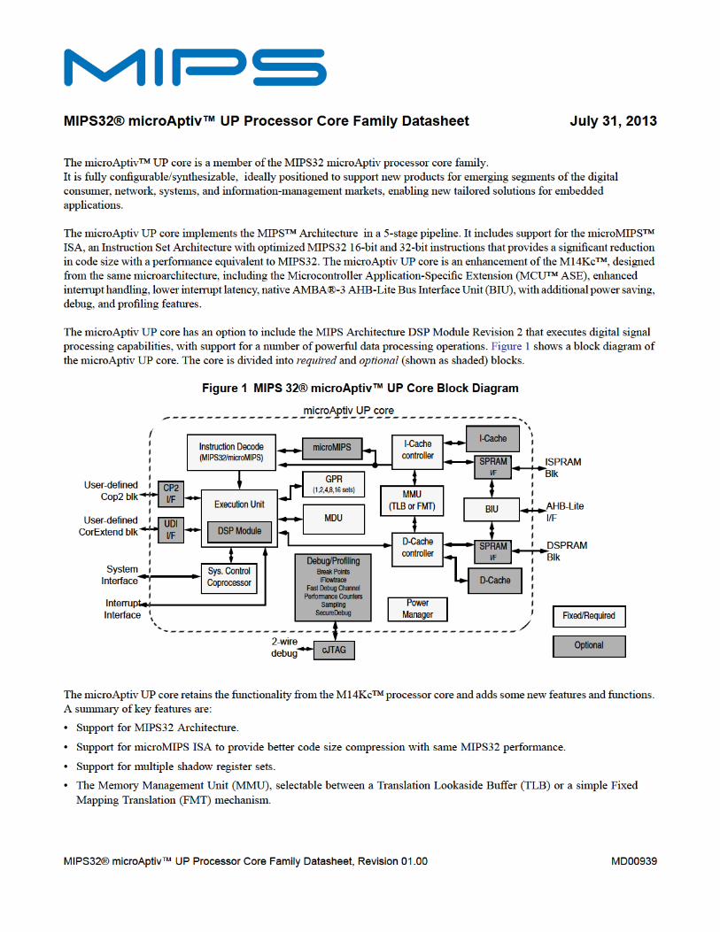
The microAptiv UP core contains both required and optionalblocks, as shown in Figure 1. Required blocks must beimplemented to remain MIPS-compliant. Optional blockscan be added to the microAptiv UP core based on the needsof the implementation.
The required blocks are as follows:
• Instruction Decode
• Execution Unit
• General Purposed Registers (GPR)
• Multiply/Divide Unit (MDU)
• System Control Coprocessor (CP0)
• Memory Management Unit (MMU)
• I/D Cache Controllers
• Bus Interface Unit (BIU)
• Power Management
Optional or configurable blocks include:
• Instruction Cache
• Data Cache
• Scratchpad RAM interface
• Configurable instruction decoder supporting three ISAmodes: MIPS32-only, MIPS32 and microMIPS, ormicroMIPS-only
• DSP (integrated with MDU)
• Coprocessor 2 interface
• CorExtend® User-Defined Instruction (UDI) interface
• Debug/Profiling with Enhanced JTAG (EJTAG)Controller, Break points, Sampling, Performancecounters, Fast Debug Channel, and iFlowtrace logic
The section "MIPS32® microAptiv™ UP Core RequiredLogic Blocks" on page 5 discusses the required blocks. Thesection "MIPS32® microAptiv™ UP Core Optional orConfigurable Logic Blocks" on page 12 discusses theoptional blocks.
Pipeline Flow
The microAptiv UP core implements a 5-stage pipeline witha performance similar to the M14Kc™ pipeline. The pipelineallows the processor to achieve high frequency whileminimizing device complexity, reducing both cost and powerconsumption.
The microAptiv UP core pipeline consists of five stages:
• Instruction (I Stage)
• Execution (E Stage)
• Memory (M Stage)
• Align (A Stage)
• Writeback (W stage)
The microAptiv UP core implements a bypass mechanismthat allows the result of an operation to be forwarded directlyto the instruction that needs it without having to write theresult to the register and then read it back.
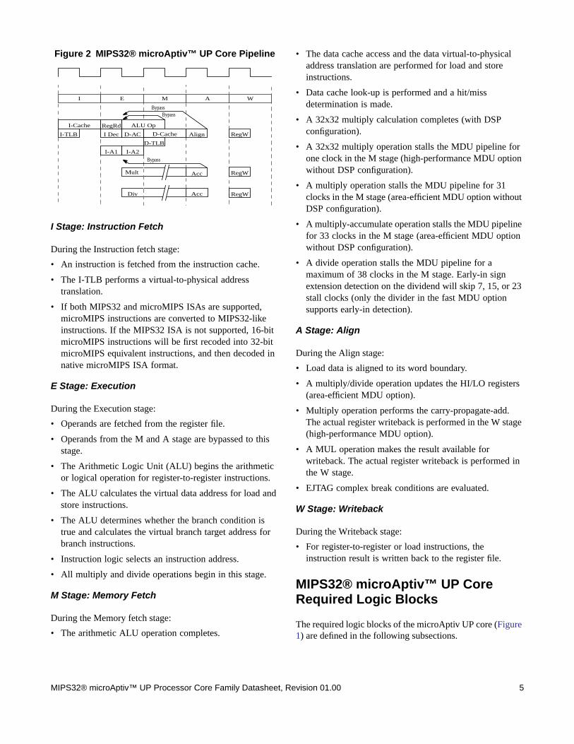
Figure 2 shows a timing diagram of the microAptiv UP corepipeline (shown with the-high performance MDUand TLBused in the MMU).
MIPS32® microAptiv™ UP Processor Core Family Datasheet, Revision 01.00 5
Figure 2 MIPS32® microAptiv™ UP Core Pipeline
I Stage: Instruction Fetch
During the Instruction fetch stage:
• An instruction is fetched from the instruction cache.
• The I-TLB performs a virtual-to-physical addresstranslation.
• If both MIPS32 and microMIPS ISAs are supported,microMIPS instructions are converted to MIPS32-likeinstructions. If the MIPS32 ISA is not supported, 16-bitmicroMIPS instructions will be first recoded into 32-bitmicroMIPS equivalent instructions, and then decoded innative microMIPS ISA format.
E Stage: Execution
During the Execution stage:
• Operands are fetched from the register file.
• Operands from the M and A stage are bypassed to thisstage.
• The Arithmetic Logic Unit (ALU) begins the arithmeticor logical operation for register-to-register instructions.
• The ALU calculates the virtual data address for load andstore instructions.
• The ALU determines whether the branch condition istrue and calculates the virtual branch target address forbranch instructions.
• Instruction logic selects an instruction address.
• All multiply and divide operations begin in this stage.
M Stage: Memory Fetch
During the Memory fetch stage:
• The arithmetic ALU operation completes.
• The data cache access and the data virtual-to-physicaladdress translation are performed for load and storeinstructions.
• Data cache look-up is performed and a hit/missdetermination is made.
• A 32x32 multiply calculation completes (with DSPconfiguration).
• A 32x32 multiply operation stalls the MDU pipeline forone clock in the M stage (high-performance MDU optionwithout DSP configuration).
• A multiply operation stalls the MDU pipeline for 31clocks in the M stage (area-efficient MDU option withoutDSP configuration).
• A multiply-accumulate operation stalls the MDU pipelinefor 33 clocks in the M stage (area-efficient MDU optionwithout DSP configuration).
• A divide operation stalls the MDU pipeline for amaximum of 38 clocks in the M stage. Early-in signextension detection on the dividend will skip 7, 15, or 23stall clocks (only the divider in the fast MDU optionsupports early-in detection).
A Stage: Align
During the Align stage:
• Load data is aligned to its word boundary.
• A multiply/divide operation updates the HI/LO registers(area-efficient MDU option).
• Multiply operation performs the carry-propagate-add.The actual register writeback is performed in the W stage(high-performance MDU option).
• A MUL operation makes the result available forwriteback. The actual register writeback is performed inthe W stage.
• EJTAG complex break conditions are evaluated.
W Stage: Writeback
During the Writeback stage:
• For register-to-register or load instructions, theinstruction result is written back to the register file.
MIPS32® microAptiv™ UP CoreRequired Logic Blocks
The required logic blocks of the microAptiv UP core (Figure1) are defined in the following subsections.
I E M A W
I-TLB
I-A1
I-Cache RegRd
I Dec
ALU Op
D-TLB
D-Cache Align RegWD-AC
BypassBypass
Mult RegW
Bypass
Acc
I-A2
Div RegWAcc
6 MIPS32® microAptiv™ UP Processor Core Family Datasheet, Revision 01.00
Execution Unit
The microAptiv UP core execution unit implements a load/store architecture with single-cycle ALU operations (logical,shift, add, subtract) and an autonomous multiply/divide unit.
The execution unit includes:
• Arithmetic Logic Unit (ALU) for performing arithmeticand bitwise logical operations. Shared adder forarithmetic operations, load/store address calculation, andbranch target calculation.
• Address unit for calculating the next PC and next fetchaddress selection muxes.
• Load Aligner.
• Shifter and Store Aligner.
• Branch condition comparator.
• Trap condition comparator.
• Bypass muxes to advance result between two adjacentinstructions with data dependency.
• Leading Zero/One detect unit for implementing the CLZand CLO instructions.
• Actual execution of the Atomic Instructions defined inthe MCU ASE.
• A separate DSP ALU and Logic block for performingpart of DSP Module instructions, such as arithmetic/shift/compare operations if the DSP function is configured.
General Purpose Registers
The microAptiv UP core contains thirty-two 32-bit general-purpose registers used for integer operations and addresscalculation. Optionally, one, three, seven or fifteen additionalregister file shadow sets (each containing thirty-two registers)can be added to minimize context switching overhead duringinterrupt/exception processing. The register file consists oftwo read ports and one write port and is fully bypassed tominimize operation latency in the pipeline.
Multiply/Divide Unit (MDU)
The microAptiv UP core includes a multiply/divide unit(MDU) that contains a separate, dedicated pipeline for integermultiply/divide operations, and DSP Module multiplyinstructions. This pipeline operates in parallel with the integerunit (IU) pipeline and does not stall when the IU pipelinestalls. This allows the long-running MDU operations to bepartially masked by system stalls and/or other integer unitinstructions.
The MIPS architecture defines that the result of a multiply ordivide operation be placed in a pair (without DSP enabled) orone of 4 pairs (with DSP enabled) of HI and LO registers.Using the Move-From-HI (MFHI) and Move-From-LO(MFLO) instructions, these values can be transferred to thegeneral-purpose register file.
There are three configuration options for the MDU: 1) a full32x32 multiplier block; 2) a higher performance 32x16multiplier block; 3) an area-efficient iterative multiplierblock. Option 2 and 3 are available if the DSP configurationoption is disabled. If the DSP configuration option is enabled,option 1 is the default. The selection of the MDU style allowsthe implementor to determine the appropriate performanceand area trade-off for the application.
MDU with 32x32 DSP Multiplier
With the DSP configuration option enabled, the MDUsupports execution of one 16x16, 32x16, or 32x32 multiply ormultiply-accumulate operation every clock cycle with thebuilt in 32x32 multiplier array. The multiplier is shared withDSP Module operations.
The MDU also implements various shift instructionsoperating on the HI/LO register and multiply instructions asdefined in the DSP Module. It supports all the data typesrequired for this purpose and includes three extra HI/LOregisters as defined by the Module.
Table 1 lists the latencies (throughput with data dependency)and repeat rates (throughput without data dependency) for theDSP multiply and dot-product operations. The approximatelatencies and repeat rates are listed in terms of pipelineclocks. For a more detailed discussion of latencies and repeatrates, refer to the MIPS32 microAptiv™ UP Processor CoreSoftware User’s Manual.
Table 1 DSP-related Latencies and Repeat Rates
Opcode LatencyRepeat
Rate
Multiply and dot-product without satu-ration after accumula-tion
5 1
Multiply and dot-product with satura-tion after accumula-tion
5 1
Multiply withoutaccumulation
5 1
MIPS32® microAptiv™ UP Processor Core Family Datasheet, Revision 01.00 7
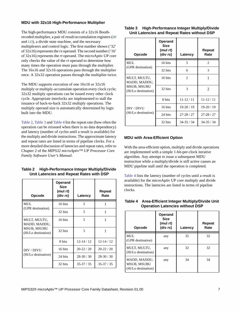
MDU with 32x16 High-Performance Multiplier
The high-performance MDU consists of a 32x16 Booth-recoded multiplier, a pair of result/accumulation registers (HIand LO), a divide state machine, and the necessarymultiplexers and control logic. The first number shown (‘32’of 32x16) represents the rs operand. The second number (‘16’of 32x16) represents the rt operand. The microAptiv UP coreonly checks the value of the rt operand to determine howmany times the operation must pass through the multiplier.The 16x16 and 32x16 operations pass through the multiplieronce. A 32x32 operation passes through the multiplier twice.
The MDU supports execution of one 16x16 or 32x16multiply or multiply-accumulate operation every clock cycle;32x32 multiply operations can be issued every other clockcycle. Appropriate interlocks are implemented to stall theissuance of back-to-back 32x32 multiply operations. Themultiply operand size is automatically determined by logicbuilt into the MDU.
Table 2, Table 3 and Table 4 list the repeat rate (how often theoperation can be reissued when there is no data dependency)and latency (number of cycles until a result is available) forthe multiply and divide instructions. The approximate latencyand repeat rates are listed in terms of pipeline clocks. For amore detailed discussion of latencies and repeat rates, refer toChapter 2 of the MIPS32 microAptiv™ UP Processor CoreFamily Software User’s Manual.
MDU with Area-Efficient Option
With the area-efficient option, multiply and divide operationsare implemented with a simple 1-bit-per-clock iterativealgorithm. Any attempt to issue a subsequent MDUinstruction while a multiply/divide is still active causes anMDU pipeline stall until the operation is completed.
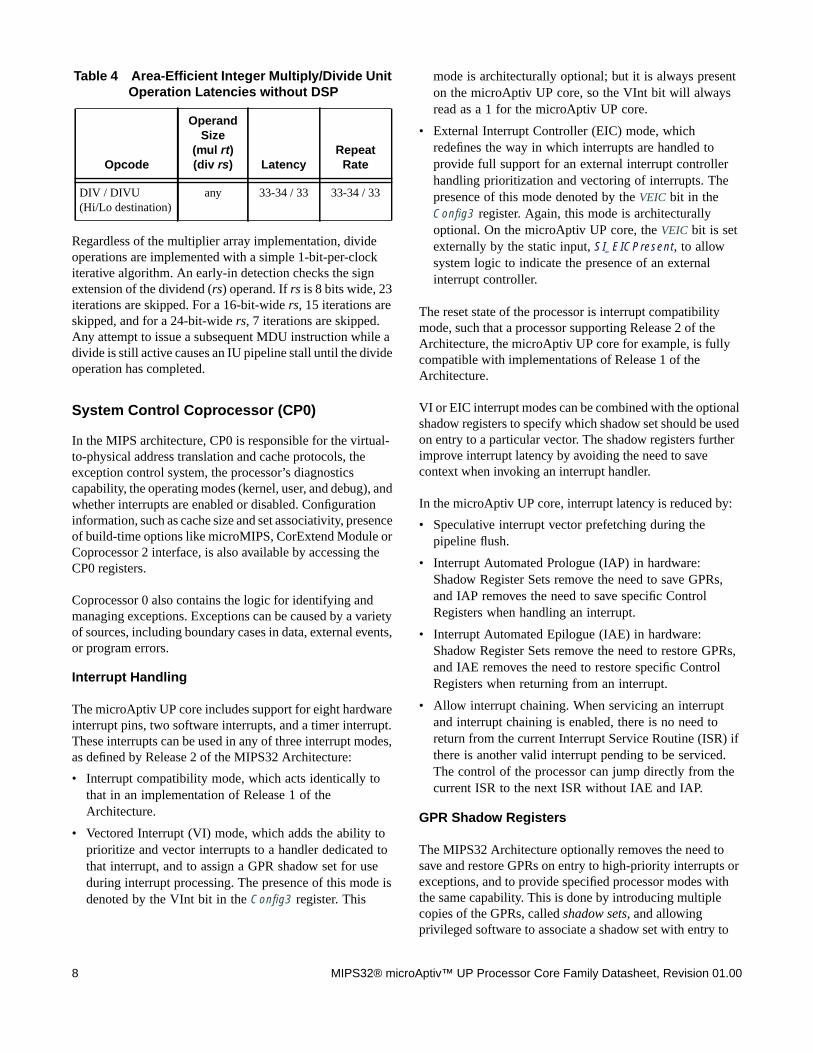
Table 4 lists the latency (number of cycles until a result isavailable) for the microAptiv UP core multiply and divideinstructions. The latencies are listed in terms of pipelineclocks.
Table 2 High-Performance Integer Multiply/DivideUnit Latencies and Repeat Rates with DSP
Opcode
OperandSize
(mul rt)(div rs) Latency
RepeatRate
MUL(GPR destination)
16 bits 5 1
32 bits 5 1
MULT, MULTU,MADD, MADDU,MSUB, MSUBU(Hi/Lo destination)
16 bits 5 1
32 bits 5 1
DIV / DIVU(Hi/Lo destination)
8 bits 12-14 / 12 12-14 / 12
16 bits 20-22 / 20 20-22 / 20
24 bits 28-30 / 30 28-30 / 30
32 bits 35-37 / 35 35-37 / 35
Table 3 High-Performance Integer Multiply/DivideUnit Latencies and Repeat Rates without DSP
Opcode
OperandSize
(mul rt)(div rs) Latency
RepeatRate
MUL(GPR destination)
16 bits 5 2
32 bits 6 3
MULT, MULTU,MADD, MADDU,MSUB, MSUBU(Hi/Lo destination)
16 bits 2 1
32 bits 3 2
DIV / DIVU(Hi/Lo destination)
8 bits 11-12 / 11 11-12 / 11
16 bits 19-20 / 19 19-20 / 19
24 bits 27-28 / 27 27-28 / 27
32 bits 34-35 / 34 34-35 / 34
Table 4 Area-Efficient Integer Multiply/Divide UnitOperation Latencies without DSP
Opcode
OperandSize
(mul rt)(div rs) Latency
RepeatRate
MUL(GPR destination)
any 35 32
MULT, MULTU,(Hi/Lo destination)
any 32 32
MADD, MADDU,MSUB, MSUBU(Hi/Lo destination)
any 34 34
8 MIPS32® microAptiv™ UP Processor Core Family Datasheet, Revision 01.00
Regardless of the multiplier array implementation, divideoperations are implemented with a simple 1-bit-per-clockiterative algorithm. An early-in detection checks the signextension of the dividend (rs) operand. If rs is 8 bits wide, 23iterations are skipped. For a 16-bit-wide rs, 15 iterations areskipped, and for a 24-bit-wide rs, 7 iterations are skipped.Any attempt to issue a subsequent MDU instruction while adivide is still active causes an IU pipeline stall until the divideoperation has completed.
System Control Coprocessor (CP0)
In the MIPS architecture, CP0 is responsible for the virtual-to-physical address translation and cache protocols, theexception control system, the processor’s diagnosticscapability, the operating modes (kernel, user, and debug), andwhether interrupts are enabled or disabled. Configurationinformation, such as cache size and set associativity, presenceof build-time options like microMIPS, CorExtend Module orCoprocessor 2 interface, is also available by accessing theCP0 registers.
Coprocessor 0 also contains the logic for identifying andmanaging exceptions. Exceptions can be caused by a varietyof sources, including boundary cases in data, external events,or program errors.
Interrupt Handling
The microAptiv UP core includes support for eight hardwareinterrupt pins, two software interrupts, and a timer interrupt.These interrupts can be used in any of three interrupt modes,as defined by Release 2 of the MIPS32 Architecture:
• Interrupt compatibility mode, which acts identically tothat in an implementation of Release 1 of theArchitecture.
• Vectored Interrupt (VI) mode, which adds the ability toprioritize and vector interrupts to a handler dedicated tothat interrupt, and to assign a GPR shadow set for useduring interrupt processing. The presence of this mode isdenoted by the VInt bit in the Config3 register. This
mode is architecturally optional; but it is always presenton the microAptiv UP core, so the VInt bit will alwaysread as a 1 for the microAptiv UP core.
• External Interrupt Controller (EIC) mode, whichredefines the way in which interrupts are handled toprovide full support for an external interrupt controllerhandling prioritization and vectoring of interrupts. Thepresence of this mode denoted by the VEIC bit in theConfig3 register. Again, this mode is architecturallyoptional. On the microAptiv UP core, the VEIC bit is setexternally by the static input, SI_EICPresent, to allowsystem logic to indicate the presence of an externalinterrupt controller.
The reset state of the processor is interrupt compatibilitymode, such that a processor supporting Release 2 of theArchitecture, the microAptiv UP core for example, is fullycompatible with implementations of Release 1 of theArchitecture.
VI or EIC interrupt modes can be combined with the optionalshadow registers to specify which shadow set should be usedon entry to a particular vector. The shadow registers furtherimprove interrupt latency by avoiding the need to savecontext when invoking an interrupt handler.
In the microAptiv UP core, interrupt latency is reduced by:
• Speculative interrupt vector prefetching during thepipeline flush.
• Interrupt Automated Prologue (IAP) in hardware:Shadow Register Sets remove the need to save GPRs,and IAP removes the need to save specific ControlRegisters when handling an interrupt.
• Interrupt Automated Epilogue (IAE) in hardware:Shadow Register Sets remove the need to restore GPRs,and IAE removes the need to restore specific ControlRegisters when returning from an interrupt.
• Allow interrupt chaining. When servicing an interruptand interrupt chaining is enabled, there is no need toreturn from the current Interrupt Service Routine (ISR) ifthere is another valid interrupt pending to be serviced.The control of the processor can jump directly from thecurrent ISR to the next ISR without IAE and IAP.
GPR Shadow Registers
The MIPS32 Architecture optionally removes the need tosave and restore GPRs on entry to high-priority interrupts orexceptions, and to provide specified processor modes withthe same capability. This is done by introducing multiplecopies of the GPRs, called shadow sets, and allowingprivileged software to associate a shadow set with entry to
DIV / DIVU(Hi/Lo destination)
any 33-34 / 33 33-34 / 33
Table 4 Area-Efficient Integer Multiply/Divide UnitOperation Latencies without DSP
Opcode
OperandSize
(mul rt)(div rs) Latency
RepeatRate
MIPS32® microAptiv™ UP Processor Core Family Datasheet, Revision 01.00 9
kernel mode via an interrupt vector or exception. The normalGPRs are logically considered shadow set zero.
The number of GPR shadow sets is a build-time option. ThemicroAptiv UP core allows 1 (the normal GPRs), 2, 4, 8, or16 shadow sets. The highest number actually implemented isindicated by the SRSCtlHSS field. If this field is zero, only thenormal GPRs are implemented.
Shadow sets are new copies of the GPRs that can besubstituted for the normal GPRs on entry to kernel mode viaan interrupt or exception. Once a shadow set is bound to akernel-mode entry condition, references to GPRs operateexactly as one would expect, but they are redirected toregisters that are dedicated to that condition. Privilegedsoftware may need to reference all GPRs in the register file,even specific shadow registers that are not visible in thecurrent mode, and the RDPGPR and WRPGPR instructionsare used for this purpose. The CSS field of the SRSCtl registerprovides the number of the current shadow register set, andthe PSS field of the SRSCtl register provides the number of theprevious shadow register set that was current before the lastexception or interrupt occurred.
If the processor is operating in VI interrupt mode, binding ofa vectored interrupt to a shadow set is done by writing to theSRSMap register. If the processor is operating in EIC interruptmode, the binding of the interrupt to a specific shadow set isprovided by the external interrupt controller and is configuredin an implementation-dependent way. Binding of anexception or non-vectored interrupt to a shadow set is doneby writing to the ESS field of the SRSCtl register. When anexception or interrupt occurs, the value of SRSCtlCSS is copiedto SRSCtlPSS, and SRSCtlCSS is set to the value taken from theappropriate source. On an ERET, the value of SRSCtlPSS iscopied back into SRSCtlCSS to restore the shadow set of themode to which control returns.
Modes of Operation
The microAptiv UP core implements three modes ofoperation:
• User mode is most often used for applications pro-grams.
• Kernel mode is typically used for handling excep-tions and operating-system kernel functions, includ-ing CP0 management and I/O device accesses.
• Debug mode is used during system bring-up andsoftware development. Refer to the EJTAG sectionfor more information on debug mode.
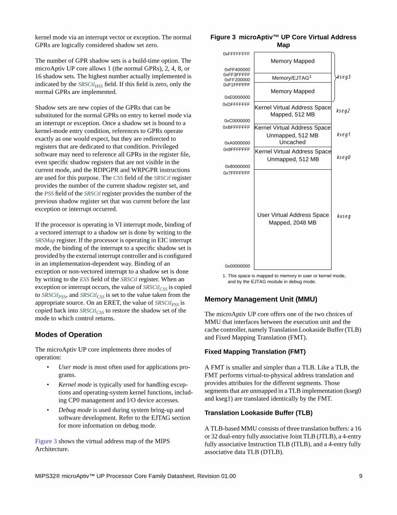
Figure 3 shows the virtual address map of the MIPSArchitecture.
Figure 3 microAptiv™ UP Core Virtual AddressMap
Memory Management Unit (MMU)
The microAptiv UP core offers one of the two choices ofMMU that interfaces between the execution unit and thecache controller, namely Translation Lookaside Buffer (TLB)and Fixed Mapping Translation (FMT).
Fixed Mapping Translation (FMT)
A FMT is smaller and simpler than a TLB. Like a TLB, theFMT performs virtual-to-physical address translation andprovides attributes for the different segments. Thosesegments that are unmapped in a TLB implementation (kseg0and kseg1) are translated identically by the FMT.
Translation Lookaside Buffer (TLB)
A TLB-based MMU consists of three translation buffers: a 16or 32 dual-entry fully associative Joint TLB (JTLB), a 4-entryfully associative Instruction TLB (ITLB), and a 4-entry fullyassociative data TLB (DTLB).
kuseg
kseg0
kseg1
kseg2
kseg3
0x00000000
0x7FFFFFFF0x80000000
0x9FFFFFFF0xA0000000
0xBFFFFFFF0xC0000000
0xDFFFFFFF
0xE0000000
0xF1FFFFFF
Kernel Virtual Address Space
Unmapped, 512 MBKernel Virtual Address Space
Uncached
Unmapped, 512 MBKernel Virtual Address Space
User Virtual Address Space
1. This space is mapped to memory in user or kernel mode,and by the EJTAG module in debug mode.
0xFF2000000xFF3FFFFF0xFF400000
0xFFFFFFFF
Memory/EJTAG1
Mapped, 2048 MB
Mapped, 512 MB
Memory Mapped
Memory Mapped
10 MIPS32® microAptiv™ UP Processor Core Family Datasheet, Revision 01.00
When an instruction address is calculated, the virtual addressis compared to the contents of the 4-entry ITLB. If the addressis not found in the ITLB, the JTLB is accessed. If the entry isfound in the JTLB, that entry is then written into the ITLB. Ifthe address is not found in the JTLB, a TLB refill exceptionis taken.
When a data address is calculated, the virtual address iscompared to both the 4-entry DTLB and the JTLB. If theaddress is not found in the DTLB, but is found in the JTLB,that address is immediately written to the DTLB. If theaddress is not found in the JTLB, a TLB refill exception istaken.
The microAptiv UP core TLB allows pages to be protected bya read-inhibit and an execute-inhibit attribute in addition tothe write-protection attribute defined by the MIPS32 PRA.
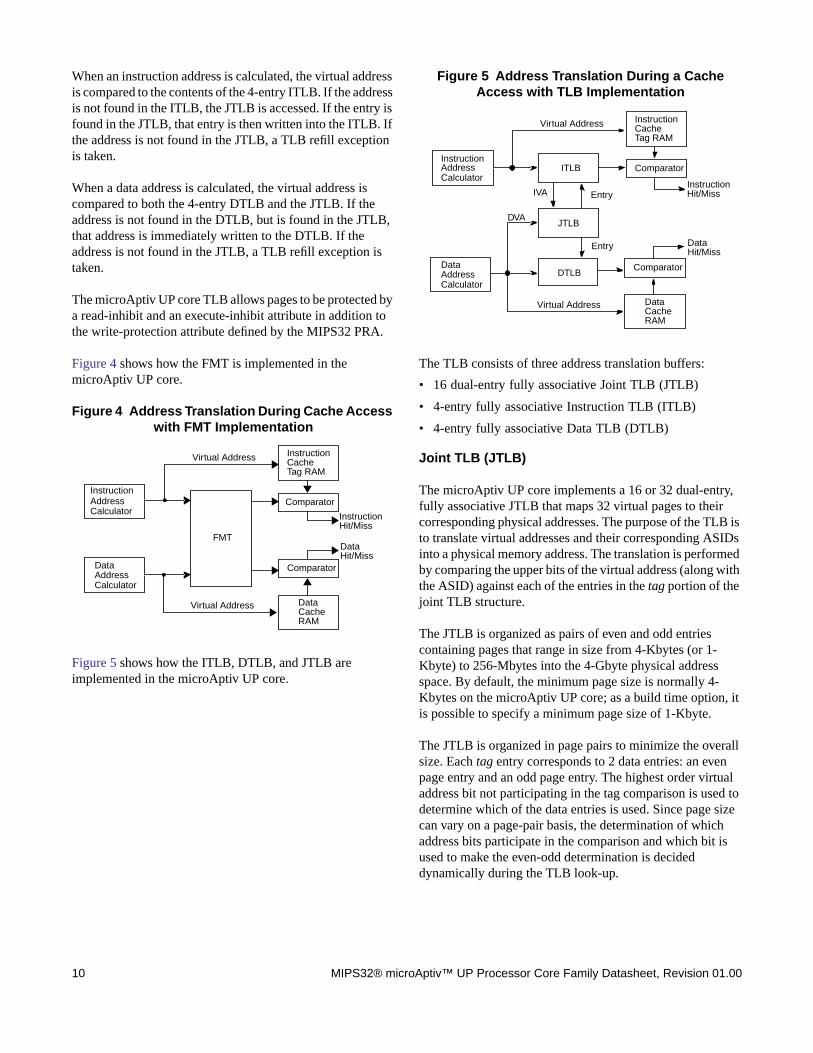
Figure 4 shows how the FMT is implemented in themicroAptiv UP core.
Figure 4 Address Translation During Cache Accesswith FMT Implementation
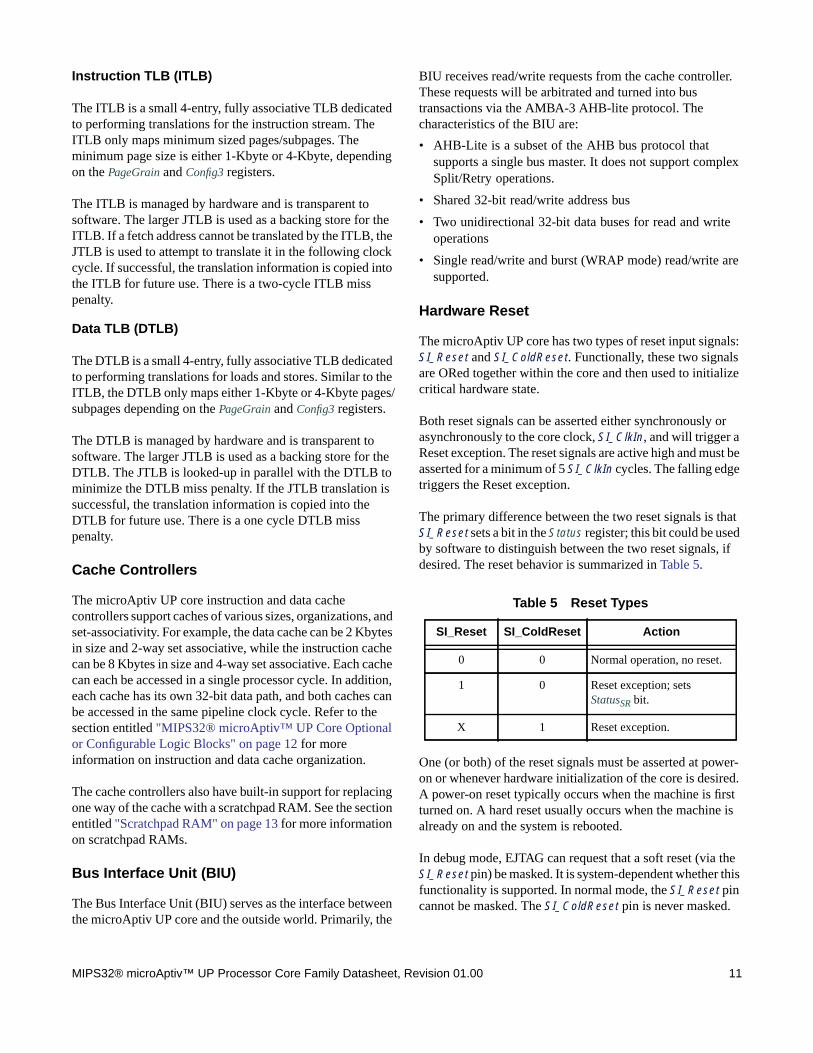
Figure 5 shows how the ITLB, DTLB, and JTLB areimplemented in the microAptiv UP core.
Figure 5 Address Translation During a CacheAccess with TLB Implementation
The TLB consists of three address translation buffers:
• 16 dual-entry fully associative Joint TLB (JTLB)
• 4-entry fully associative Instruction TLB (ITLB)
• 4-entry fully associative Data TLB (DTLB)
Joint TLB (JTLB)
The microAptiv UP core implements a 16 or 32 dual-entry,fully associative JTLB that maps 32 virtual pages to theircorresponding physical addresses. The purpose of the TLB isto translate virtual addresses and their corresponding ASIDsinto a physical memory address. The translation is performedby comparing the upper bits of the virtual address (along withthe ASID) against each of the entries in the tag portion of thejoint TLB structure.
The JTLB is organized as pairs of even and odd entriescontaining pages that range in size from 4-Kbytes (or 1-Kbyte) to 256-Mbytes into the 4-Gbyte physical addressspace. By default, the minimum page size is normally 4-Kbytes on the microAptiv UP core; as a build time option, itis possible to specify a minimum page size of 1-Kbyte.
The JTLB is organized in page pairs to minimize the overallsize. Each tag entry corresponds to 2 data entries: an evenpage entry and an odd page entry. The highest order virtualaddress bit not participating in the tag comparison is used todetermine which of the data entries is used. Since page sizecan vary on a page-pair basis, the determination of whichaddress bits participate in the comparison and which bit isused to make the even-odd determination is decideddynamically during the TLB look-up.
InstructionAddressCalculator
FMT
DataAddressCalculator
Comparator
Comparator
InstructionCacheTag RAM
DataCacheRAM
Virtual Address
Virtual Address
InstructionHit/Miss
DataHit/Miss
InstructionAddressCalculator
ITLB
DTLBDataAddressCalculator
Comparator
Comparator
InstructionCacheTag RAM
DataCacheRAM
Virtual Address
Virtual Address
InstructionHit/Miss
DataHit/Miss
JTLB
IVA Entry
Entry
DVA
MIPS32® microAptiv™ UP Processor Core Family Datasheet, Revision 01.00 11
Instruction TLB (ITLB)
The ITLB is a small 4-entry, fully associative TLB dedicatedto performing translations for the instruction stream. TheITLB only maps minimum sized pages/subpages. Theminimum page size is either 1-Kbyte or 4-Kbyte, dependingon the PageGrain and Config3 registers.
The ITLB is managed by hardware and is transparent tosoftware. The larger JTLB is used as a backing store for theITLB. If a fetch address cannot be translated by the ITLB, theJTLB is used to attempt to translate it in the following clockcycle. If successful, the translation information is copied intothe ITLB for future use. There is a two-cycle ITLB misspenalty.
Data TLB (DTLB)
The DTLB is a small 4-entry, fully associative TLB dedicatedto performing translations for loads and stores. Similar to theITLB, the DTLB only maps either 1-Kbyte or 4-Kbyte pages/subpages depending on the PageGrain and Config3 registers.
The DTLB is managed by hardware and is transparent tosoftware. The larger JTLB is used as a backing store for theDTLB. The JTLB is looked-up in parallel with the DTLB tominimize the DTLB miss penalty. If the JTLB translation issuccessful, the translation information is copied into theDTLB for future use. There is a one cycle DTLB misspenalty.
Cache Controllers
The microAptiv UP core instruction and data cachecontrollers support caches of various sizes, organizations, andset-associativity. For example, the data cache can be 2 Kbytesin size and 2-way set associative, while the instruction cachecan be 8 Kbytes in size and 4-way set associative. Each cachecan each be accessed in a single processor cycle. In addition,each cache has its own 32-bit data path, and both caches canbe accessed in the same pipeline clock cycle. Refer to thesection entitled "MIPS32® microAptiv™ UP Core Optionalor Configurable Logic Blocks" on page 12 for moreinformation on instruction and data cache organization.
The cache controllers also have built-in support for replacingone way of the cache with a scratchpad RAM. See the sectionentitled "Scratchpad RAM" on page 13 for more informationon scratchpad RAMs.
Bus Interface Unit (BIU)
The Bus Interface Unit (BIU) serves as the interface betweenthe microAptiv UP core and the outside world. Primarily, the
BIU receives read/write requests from the cache controller.These requests will be arbitrated and turned into bustransactions via the AMBA-3 AHB-lite protocol. Thecharacteristics of the BIU are:
• AHB-Lite is a subset of the AHB bus protocol thatsupports a single bus master. It does not support complexSplit/Retry operations.
• Shared 32-bit read/write address bus
• Two unidirectional 32-bit data buses for read and writeoperations
• Single read/write and burst (WRAP mode) read/write aresupported.
Hardware Reset
The microAptiv UP core has two types of reset input signals:SI_Reset and SI_ColdReset. Functionally, these two signalsare ORed together within the core and then used to initializecritical hardware state.
Both reset signals can be asserted either synchronously orasynchronously to the core clock, SI_ClkIn, and will trigger aReset exception. The reset signals are active high and must beasserted for a minimum of 5 SI_ClkIn cycles. The falling edgetriggers the Reset exception.
The primary difference between the two reset signals is thatSI_Reset sets a bit in the Status register; this bit could be usedby software to distinguish between the two reset signals, ifdesired. The reset behavior is summarized in Table 5.
One (or both) of the reset signals must be asserted at power-on or whenever hardware initialization of the core is desired.A power-on reset typically occurs when the machine is firstturned on. A hard reset usually occurs when the machine isalready on and the system is rebooted.
In debug mode, EJTAG can request that a soft reset (via theSI_Reset pin) be masked. It is system-dependent whether thisfunctionality is supported. In normal mode, the SI_Reset pincannot be masked. The SI_ColdReset pin is never masked.
Table 5 Reset Types
SI_Reset SI_ColdReset Action
0 0 Normal operation, no reset.
1 0 Reset exception; setsStatusSR bit.
X 1 Reset exception.
12 MIPS32® microAptiv™ UP Processor Core Family Datasheet, Revision 01.00
Power Management
The microAptiv UP core offers a number of powermanagement features, including low-power design, activepower management, and power-down modes of operation.The core is a static design that supports slowing or halting theclocks, which reduces system power consumption during idleperiods.
The microAptiv UP core provides two mechanisms forsystem-level low-power support:
• Register-controlled power management
• Instruction-controlled power management
Register-Controlled Power Management
The RP bit in the CP0 Status register provides a softwaremechanism for placing the system into a low-power state.The state of the RP bit is available externally via the SI_RPsignal. The external agent then decides whether to place thedevice in a low-power mode, such as reducing the systemclock frequency.
Three additional bits,StatusEXL, StatusERL, and DebugDMsupport the power management function by allowing the userto change the power state if an exception or error occurs whilethe microAptiv UP core is in a low-power state. Dependingon what type of exception is taken, one of these three bits willbe asserted and reflected on the SI_EXL, SI_ERL, orEJ_DebugM outputs. The external agent can look at thesesignals and determine whether to leave the low-power state toservice the exception.
The following four power-down signals are part of the systeminterface and change state as the corresponding bits in theCP0 registers are set or cleared:
• The SI_RP signal represents the state of the RP bit (27) inthe CP0 Status register.
• The SI_EXL signal represents the state of the EXL bit (1)in the CP0 Status register.
• The SI_ERL signal represents the state of the ERL bit (2)in the CP0 Status register.
• The EJ_DebugM signal represents the state of the DM bit(30) in the CP0 Debug register.
Instruction-Controlled Power Management
The second mechanism for invoking power-down mode is byexecuting the WAIT instruction. When the WAIT instructionis executed, the internal clock is suspended; however, theinternal timer and some of the input pins (SI_Int[5:0], SI_NMI,SI_Reset, and SI_ColdReset) continue to run. Once the CPUis in instruction-controlled power management mode, any
interrupt, NMI, or reset condition causes the CPU to exit thismode and resume normal operation.
The microAptiv UP core asserts the SI_Sleep signal, which ispart of the system interface bus, whenever the WAITinstruction is executed. The assertion of SI_Sleep indicatesthat the clock has stopped and the microAptiv UP core iswaiting for an interrupt.
Local clock gating
The majority of the power consumed by the microAptiv UPcore is in the clock tree and clocking registers. The core hassupport for extensive use of local gated-clocks. Power-conscious implementors can use these gated clocks tosignificantly reduce power consumption within the core.
MIPS32® microAptiv™ UP CoreOptional or Configurable LogicBlocks
The microAptiv UP core contains several optional orconfigurable logic blocks, shown as shaded in the blockdiagram in Figure 1.
Instruction Cache
The instruction cache is an optional on-chip memory block ofup to 64 Kbytes. Because the instruction cache is virtuallyindexed, the virtual-to-physical address translation occurs inparallel with the cache access rather than having to wait forthe physical address translation. The tag holds 22 bits ofphysical address, a valid bit, and a lock bit. The LRUreplacement bits (0-6b per set depending on associativity) arestored in a separate array.
The instruction cache block also contains and manages theinstruction line fill buffer. Besides accumulating data to bewritten to the cache, instruction fetches that reference data inthe line fill buffer are serviced either by a bypass of that data,or data coming from the external interface. The instructioncache control logic controls the bypass function.
The microAptiv UP core supports instruction-cache locking.Cache locking allows critical code or data segments to belocked into the cache on a “per-line” basis, enabling thesystem programmer to maximize the efficiency of the systemcache.
The cache-locking function is always available on allinstruction-cache entries. Entries can then be marked aslocked or unlocked on a per entry basis using the CACHEinstruction.
MIPS32® microAptiv™ UP Processor Core Family Datasheet, Revision 01.00 13
Data Cache
The data cache is an optional on-chip memory block of up to64 Kbytes. This virtually indexed, physically tagged cache isprotected. Because the data cache is virtually indexed, thevirtual-to-physical address translation occurs in parallel withthe cache access. The tag holds 22 bits of physical address, avalid bit, and a lock bit. There is an additional array holdingdirty bits and LRU replacement algorithm bits (0-6bdepending on associativity) for each set of the cache.
In addition to instruction-cache locking, the microAptiv UPcore also supports a data-cache locking mechanism identicalto the instruction cache. Critical data segments are locked intothe cache on a “per-line” basis. The locked contents can beupdated on a store hit, but cannot be selected for replacementon a cache miss.
The cache-locking function is always available on all datacache entries. Entries can then be marked as locked orunlocked on a per-entry basis using the CACHE instruction.
Cache Memory Configuration
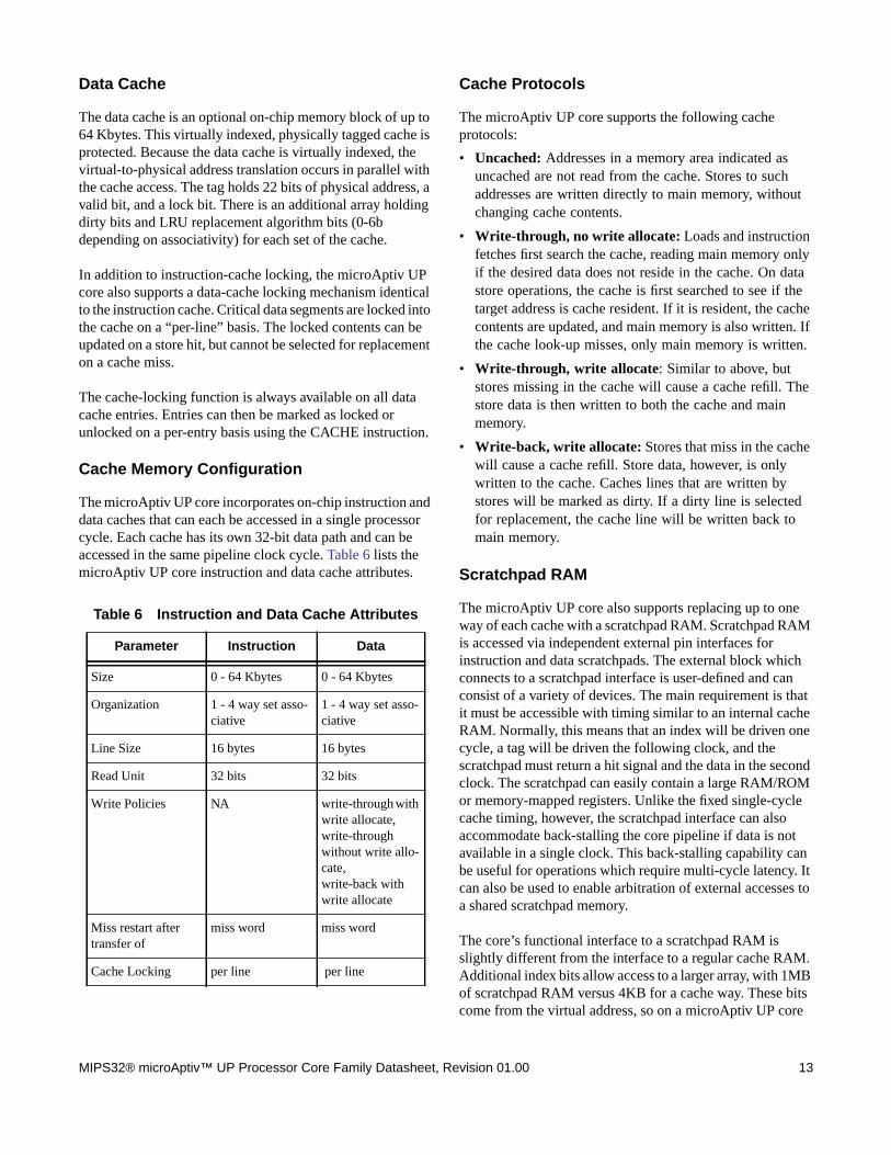
The microAptiv UP core incorporates on-chip instruction anddata caches that can each be accessed in a single processorcycle. Each cache has its own 32-bit data path and can beaccessed in the same pipeline clock cycle. Table 6 lists themicroAptiv UP core instruction and data cache attributes.
Cache Protocols
The microAptiv UP core supports the following cacheprotocols:
• Uncached: Addresses in a memory area indicated asuncached are not read from the cache. Stores to suchaddresses are written directly to main memory, withoutchanging cache contents.
• Write-through, no write allocate: Loads and instructionfetches first search the cache, reading main memory onlyif the desired data does not reside in the cache. On datastore operations, the cache is first searched to see if thetarget address is cache resident. If it is resident, the cachecontents are updated, and main memory is also written. Ifthe cache look-up misses, only main memory is written.
• Write-through, write allocate: Similar to above, butstores missing in the cache will cause a cache refill. Thestore data is then written to both the cache and mainmemory.
• Write-back, write allocate: Stores that miss in the cachewill cause a cache refill. Store data, however, is onlywritten to the cache. Caches lines that are written bystores will be marked as dirty. If a dirty line is selectedfor replacement, the cache line will be written back tomain memory.
Scratchpad RAM
The microAptiv UP core also supports replacing up to oneway of each cache with a scratchpad RAM. Scratchpad RAMis accessed via independent external pin interfaces forinstruction and data scratchpads. The external block whichconnects to a scratchpad interface is user-defined and canconsist of a variety of devices. The main requirement is thatit must be accessible with timing similar to an internal cacheRAM. Normally, this means that an index will be driven onecycle, a tag will be driven the following clock, and thescratchpad must return a hit signal and the data in the secondclock. The scratchpad can easily contain a large RAM/ROMor memory-mapped registers. Unlike the fixed single-cyclecache timing, however, the scratchpad interface can alsoaccommodate back-stalling the core pipeline if data is notavailable in a single clock. This back-stalling capability canbe useful for operations which require multi-cycle latency. Itcan also be used to enable arbitration of external accesses toa shared scratchpad memory.
The core’s functional interface to a scratchpad RAM isslightly different from the interface to a regular cache RAM.Additional index bits allow access to a larger array, with 1MBof scratchpad RAM versus 4KB for a cache way. These bitscome from the virtual address, so on a microAptiv UP core
Table 6 Instruction and Data Cache Attributes
Parameter Instruction Data
Size 0 - 64 Kbytes 0 - 64 Kbytes
Organization 1 - 4 way set asso-ciative
1 - 4 way set asso-ciative
Line Size 16 bytes 16 bytes
Read Unit 32 bits 32 bits
Write Policies NA write-through withwrite allocate,write-throughwithout write allo-cate,write-back withwrite allocate
Miss restart aftertransfer of
miss word miss word
Cache Locking per line per line
14 MIPS32® microAptiv™ UP Processor Core Family Datasheet, Revision 01.00
care must be taken to avoid virtual aliasing. The core does notautomatically refill the scratchpad way and will not select itfor replacement on cache misses.
microMIPS™ ISA
The microAptiv UP core supports the microMIPS ISA, whichcontains all MIPS32 ISA instructions (except for branch-likely instructions) in a new 32-bit encoding scheme, withsome of the commonly used instructions also available in 16-bit encoded format. This ISA improves code density throughthe additional 16-bit instructions while maintaining aperformance similar to MIPS32 mode. In microMIPS mode,16-bit or 32-bit instructions will be fetched and recoded tolegacy MIPS32 instruction opcodes in the pipeline’s I stage,so that the microAptiv UP core can have the same M14Kc™microarchitecture. Because the microMIPS instructionstream can be intermixed with 16-bit halfword or 32-bit wordsize instructions on halfword or word boundaries, additionallogic is in place to address the word misalignment issues, thusminimizing performance loss.
Depending on the optimization preference when bothMIPS32 and microMIPS ISAs are configured, themicroMIPS can be configured in performance mode, withmultiple recoding blocks being executed in parallel with Tagcompare for each Way Associativity, or with a singlerecoding block after the Tag compare logic to improve areausage.
DSP Module
The microAptiv UP core implements an optional DSPModule to benefit a wide range of DSP, Media, and DSP-likealgorithms. The DSP module is highly integrated with theExecution Unit and the MDU in order to share common logicand to include support for operations on fractional data types,saturating arithmetic, and register SIMD operations.Fractional data types Q15 and Q31 are supported. RegisterSIMD operations can perform up to four simultaneous add,subtract, or shift operations and two simultaneous multiplyoperations.
In addition, the DSP Module includes some key features thatefficiently address specific problems often encountered inDSP applications. These include, for example, support forcomplex multiply, variable-bit insert and extract, andimplementation and use of virtual circular buffers. Theextension also makes available three additional sets of HI-LOaccumulators to better facilitate common accumulatefunctions such as filter operation and convolutions.
Coprocessor 2 Interface
The microAptiv UP core can be configured to have aninterface for an on-chip coprocessor. This coprocessor can betightly coupled to the processor core, allowing high-performance solutions integrating a graphics accelerator orDSP, for example.
The coprocessor interface is extensible and standardized onMIPS cores, allowing for design reuse. The microAptiv UPcore supports a subset of the full coprocessor interfacestandard: 32b data transfer, no Coprocessor 1 support, singleissue in-order data transfer to coprocessor, one out-of-orderdata transfer from coprocessor.
The coprocessor interface is designed to ease integration withcustomer IP. The interface allows high-performancecommunication between the core and coprocessor. There areno late or critical signals on the interface.
CorExtend® User-defined InstructionExtensions
An optional CorExtend User-defined Instruction (UDI) blockenables the implementation of a small number of application-specific instructions that are tightly coupled to the core’sexecution unit. The interface to the UDI block is external tothe microAptiv UP core.
Such instructions may operate on a general-purpose register,immediate data specified by the instruction word, or localstate stored within the UDI block. The destination may be ageneral-purpose register or local UDI state. The operationmay complete in one cycle or multiple cycles, if desired.
EJTAG Debug Support
The microAptiv UP core provides for an Enhanced JTAG(EJTAG) interface for use in the software debug ofapplication and kernel code. In addition to standard usermode and kernel modes of operation, the microAptiv UP coreprovides a Debug mode that is entered after a debug exception(derived from a hardware breakpoint, single-step exception,etc.) is taken and continues until a debug exception return(DERET) instruction is executed. During this time, theprocessor executes the debug exception handler routine.
The EJTAG interface operates through the Test Access Port(TAP), a serial communication port used for transferring testdata in and out of the microAptiv UP core. In addition to thestandard JTAG instructions, special instructions defined inthe EJTAG specification specify which registers are selectedand how they are used.
MIPS32® microAptiv™ UP Processor Core Family Datasheet, Revision 01.00 15
Debug Registers
Four debug registers (DEBUG, DEBUG2, DEPC, and DESAVE)have been added to the MIPS Coprocessor 0 (CP0) registerset. The DEBUG and DEBUG2 registers show the cause of thedebug exception and are used for setting up single-stepoperations. The DEPC (Debug Exception Program Counter)register holds the address on which the debug exception wastaken, which is used to resume program execution after thedebug operation finishes. Finally, the DESAVE (DebugException Save) register enables the saving of general-purpose registers used during execution of the debugexception handler.
To exit debug mode, a Debug Exception Return (DERET)instruction is executed. When this instruction is executed, thesystem exits debug mode, allowing normal execution ofapplication and system code to resume.
EJTAG Hardware Breakpoints
There are several types of simple hardware breakpointsdefined in the EJTAG specification. These stop the normaloperation of the CPU and force the system into debug mode.There are two types of simple hardware breakpointsimplemented in the microAptiv UP core: Instructionbreakpoints and Data breakpoints. Additionally, complexhardware breakpoints can be included, which allow detectionof more intricate sequences of events.
The microAptiv UP core can be configured with thefollowing breakpoint options:
• No data or instruction, or complex breakpoints
• One data and two instruction breakpoints, withoutcomplex breakpoints
• Two data and four instruction breakpoints, withoutcomplex breakpoints
• Two data and six instruction breakpoints, with or withoutcomplex breakpoints
• Four data and eight instruction breakpoints, with orwithout complex breakpoints
Instruction breakpoints occur on instruction executionoperations, and the breakpoint is set on the virtualaddress.Instruction breakpoints can also be made on theASID value used by the MMU. A mask can be applied to thevirtual address to set breakpoints on a binary range ofinstructions.
Data breakpoints occur on load/store transactions, and thebreakpoint is set on a set of virtual address and ASID values,with the same single address or binary address range as theInstruction breakpoint. Data breakpoints can be set on a load,
a store, or both. Data breakpoints can also be set to match onthe operand value of the load/store operation, with byte-granularity masking. Finally, masks can be applied to boththe virtual address and the load/store value.
In addition, the microAptiv UP core has a configurablefeature to support data and instruction address-rangetriggered breakpoints, where a breakpoint can occur when avirtual address is either within or outside a pair of 32-bitaddresses. Unlike the traditional address-mask control,address-range triggering is not restricted to a power-of-twobinary boundary.
Complex breakpoints utilize the simple instruction and databreakpoints and break when combinations of events are seen.Complex break features include:
• Pass Counters - Each time a matching condition is seen, acounter is decremented. The break or trigger will only beenabled when the counter has counted down to 0.
• Tuples - A tuple is the pairing of an instruction and adata breakpoint. The tuple will match if both the virtualaddress of the load or store instruction matches theinstruction breakpoint, and the data breakpoint of theresulting load or store address and optional data valuematches.
• Priming - This allows a breakpoint to be enabled onlyafter other break conditions have been met. Also calledsequential or armed triggering.
• Qualified - This feature uses a data breakpoint to qualifywhen an instruction breakpoint can be taken. Once a loadmatches the data address and the data value, theinstruction break will be enabled. If a load matches theaddress, but has mis-matching data, the instruction breakwill be disabled.
Performance Counters
Performance counters are used to accumulate occurrences ofinternal predefined events/cycles/conditions for programanalysis, debug, or profiling. A few examples of event typesare clock cycles, instructions executed, specific instructiontypes executed, loads, stores, exceptions, and cycles while theCPU is stalled. There are two, 32-bit counters. Each can countone of the 64 internal predefined events selected by acorresponding control register. A counter overflow can beprogrammed to generate an interrupt, where the interrupthandler software can maintain larger total counts.
PC/Address Sampling
This sampling function is used for program profiling and hot-spots analysis. Instruction PC and/or Load/Store addressescan be sampled periodically. The result is scanned out
16 MIPS32® microAptiv™ UP Processor Core Family Datasheet, Revision 01.00
through the EJTAG port. The Debug Control Register (DCR)is used to specify the sample period and the sample trigger.
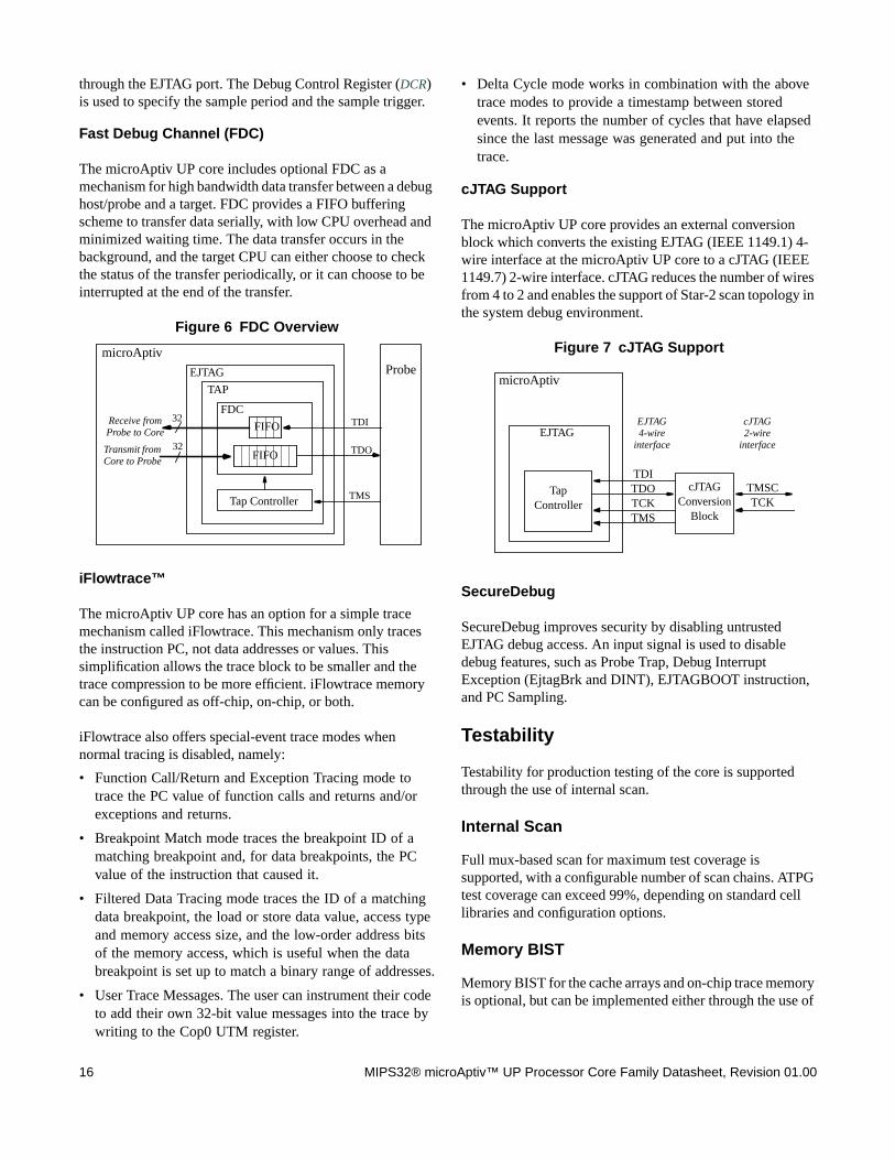
Fast Debug Channel (FDC)
The microAptiv UP core includes optional FDC as amechanism for high bandwidth data transfer between a debughost/probe and a target. FDC provides a FIFO bufferingscheme to transfer data serially, with low CPU overhead andminimized waiting time. The data transfer occurs in thebackground, and the target CPU can either choose to checkthe status of the transfer periodically, or it can choose to beinterrupted at the end of the transfer.
Figure 6 FDC Overview
iFlowtrace™
The microAptiv UP core has an option for a simple tracemechanism called iFlowtrace. This mechanism only tracesthe instruction PC, not data addresses or values. Thissimplification allows the trace block to be smaller and thetrace compression to be more efficient. iFlowtrace memorycan be configured as off-chip, on-chip, or both.
iFlowtrace also offers special-event trace modes whennormal tracing is disabled, namely:
• Function Call/Return and Exception Tracing mode totrace the PC value of function calls and returns and/orexceptions and returns.
• Breakpoint Match mode traces the breakpoint ID of amatching breakpoint and, for data breakpoints, the PCvalue of the instruction that caused it.
• Filtered Data Tracing mode traces the ID of a matchingdata breakpoint, the load or store data value, access typeand memory access size, and the low-order address bitsof the memory access, which is useful when the databreakpoint is set up to match a binary range of addresses.
• User Trace Messages. The user can instrument their codeto add their own 32-bit value messages into the trace bywriting to the Cop0 UTM register.
• Delta Cycle mode works in combination with the abovetrace modes to provide a timestamp between storedevents. It reports the number of cycles that have elapsedsince the last message was generated and put into thetrace.
cJTAG Support
The microAptiv UP core provides an external conversionblock which converts the existing EJTAG (IEEE 1149.1) 4-wire interface at the microAptiv UP core to a cJTAG (IEEE1149.7) 2-wire interface. cJTAG reduces the number of wiresfrom 4 to 2 and enables the support of Star-2 scan topology inthe system debug environment.
Figure 7 cJTAG Support
SecureDebug
SecureDebug improves security by disabling untrustedEJTAG debug access. An input signal is used to disabledebug features, such as Probe Trap, Debug InterruptException (EjtagBrk and DINT), EJTAGBOOT instruction,and PC Sampling.
Testability
Testability for production testing of the core is supportedthrough the use of internal scan.
Internal Scan
Full mux-based scan for maximum test coverage issupported, with a configurable number of scan chains. ATPGtest coverage can exceed 99%, depending on standard celllibraries and configuration options.
Memory BIST
Memory BIST for the cache arrays and on-chip trace memoryis optional, but can be implemented either through the use of
microAptivProbeEJTAG
TAP
FDC
Tap Controller
TDI
TDO
TMS
FIFOReceive fromProbe to Core
Transmit fromCore to Probe FIFO
32
32
TapController
microAptiv
EJTAGEJTAG4-wire
interface
TDITDOTCKTMS
TMSCTCK
cJTAGConversion
Block
cJTAG2-wire
interface
MIPS32® microAptiv™ UP Processor Core Family Datasheet, Revision 01.00 17
integrated BIST features provided with the core, or insertedwith an industry-standard memory BIST CAD tool.
Integrated Memory BIST
The core provides an integrated memory BIST solution fortesting the internal cache SRAMs, using BIST controllers andlogic that are tightly coupled to the cache subsystem. Severalparameters associated with the integrated BIST controllersare configurable, including the algorithm (March C+ or IFA-13).
User-specified Memory BIST
Memory BIST can also be inserted with a CAD tool or otheruser-specified method. Wrapper modules and special side-band signal buses of configurable width are provided withinthe core to facilitate this approach.
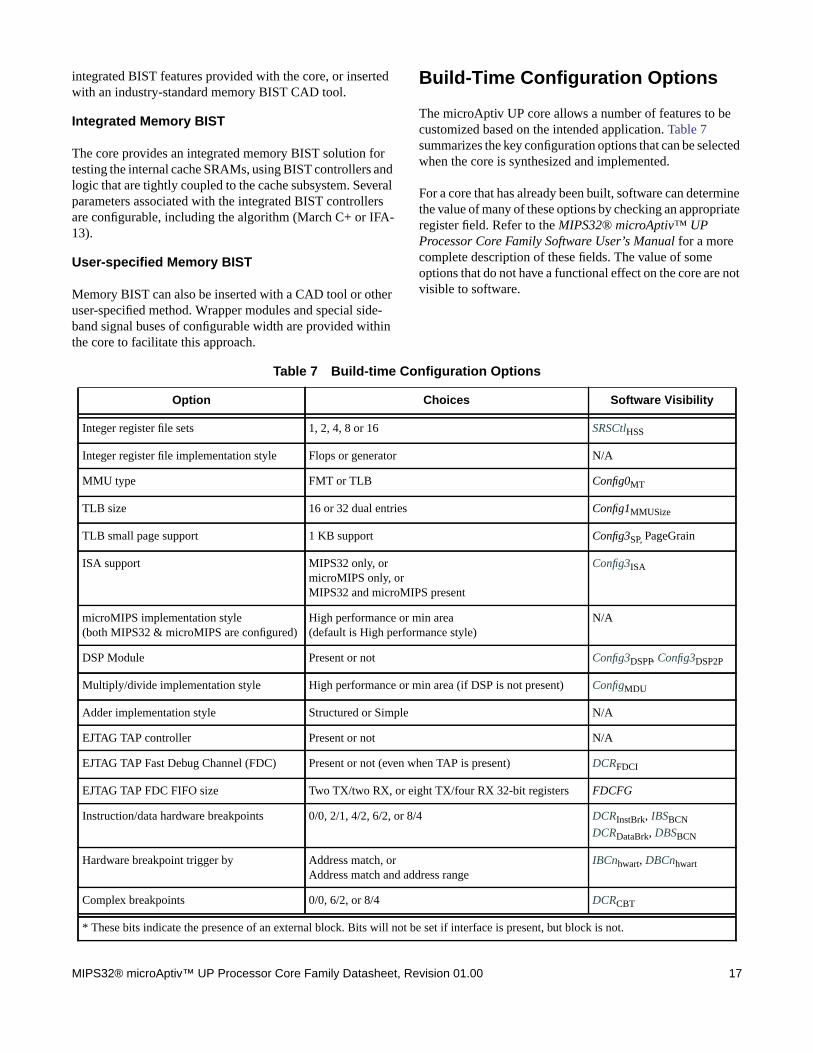
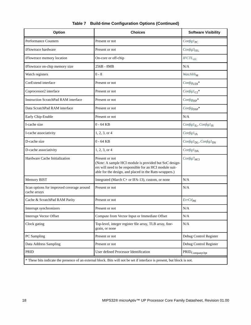
Build-Time Configuration Options
The microAptiv UP core allows a number of features to becustomized based on the intended application. Table 7summarizes the key configuration options that can be selectedwhen the core is synthesized and implemented.
For a core that has already been built, software can determinethe value of many of these options by checking an appropriateregister field. Refer to the MIPS32® microAptiv™ UPProcessor Core Family Software User’s Manual for a morecomplete description of these fields. The value of someoptions that do not have a functional effect on the core are notvisible to software.
Table 7 Build-time Configuration Options
Option Choices Software Visibility
Integer register file sets 1, 2, 4, 8 or 16 SRSCtlHSS
Integer register file implementation style Flops or generator N/A
MMU type FMT or TLB Config0MT
TLB size 16 or 32 dual entries Config1MMUSize
TLB small page support 1 KB support Config3SP, PageGrain
ISA support MIPS32 only, ormicroMIPS only, orMIPS32 and microMIPS present
Config3ISA
microMIPS implementation style(both MIPS32 & microMIPS are configured)
High performance or min area(default is High performance style)
N/A
DSP Module Present or not Config3DSPP, Config3DSP2P
Multiply/divide implementation style High performance or min area (if DSP is not present) ConfigMDU
Adder implementation style Structured or Simple N/A
EJTAG TAP controller Present or not N/A
EJTAG TAP Fast Debug Channel (FDC) Present or not (even when TAP is present) DCRFDCI
EJTAG TAP FDC FIFO size Two TX/two RX, or eight TX/four RX 32-bit registers FDCFG
Instruction/data hardware breakpoints 0/0, 2/1, 4/2, 6/2, or 8/4 DCRInstBrk, IBSBCN
DCRDataBrk, DBSBCN
Hardware breakpoint trigger by Address match, orAddress match and address range
IBCnhwart, DBCnhwart
Complex breakpoints 0/0, 6/2, or 8/4 DCRCBT
* These bits indicate the presence of an external block. Bits will not be set if interface is present, but block is not.
18 MIPS32® microAptiv™ UP Processor Core Family Datasheet, Revision 01.00
Performance Counters Present or not Config1PC
iFlowtrace hardware Present or not Config3ITL
iFlowtrace memory location On-core or off-chip IFCTLofc
iFlowtrace on-chip memory size 256B - 8MB N/A
Watch registers 0 - 8 WatchHiM
CorExtend interface Present or not ConfigUDI*
Coprocessor2 interface Present or not Config1C2*
Instruction ScratchPad RAM interface Present or not ConfigISP*
Data ScratchPad RAM interface Present or not ConfigDSP*
Early Chip-Enable Present or not N/A
I-cache size 0 - 64 KB Config1IL, Config1IS
I-cache associativity 1, 2, 3, or 4 Config1IA
D-cache size 0 - 64 KB Config1DL, Config1DS
D-cache associativity 1, 2, 3, or 4 Config1DA
Hardware Cache Initialization Present or not(Note: A sample HCI module is provided but SoC design-ers will need to be responsible for an HCI module suit-able for the design, and placed in the Ram-wrappers.)
Config7HCI
Memory BIST Integrated (March C+ or IFA-13), custom, or none N/A
Scan options for improved coverage aroundcache arrays
Present or not N/A
Cache & ScratchPad RAM Parity Present or not ErrCtlPE
Interrupt synchronizers Present or not N/A
Interrupt Vector Offset Compute from Vector Input or Immediate Offset N/A
Clock gating Top-level, integer register file array, TLB array, fine-grain, or none
N/A
PC Sampling Present or not Debug Control Register
Data Address Sampling Present or not Debug Control Register
PRID User defined Processor Identification PRIDCompanyOpt
Table 7 Build-time Configuration Options (Continued)
Option Choices Software Visibility
* These bits indicate the presence of an external block. Bits will not be set if interface is present, but block is not.
MIPS32® microAptiv™ UP Processor Core Family Datasheet, Revision 01.00 19
Revision History
Revision Date Description
01.00 July 31, 2013 • Initial 3_0_0 General Availability release

20 MIPS32® microAptiv™ UP Processor Core Family Datasheet, Revision 01.00

Unpublished rights (if any) reserved under the copyright laws of the United States of America and other countries. This document contains information that is proprietary to MIPS Tech, LLC, a Wave Computing company (“MIPS”) and MIPS’ affiliates as applicable. Any copying, reproducing, modifying or use of this information (in whole or in part) that is not expressly permitted in writing by MIPS or MIPS’ affiliates as applicable or an authorized third party is strictly prohibited. At a minimum, this information is protected under unfair competition and copyright laws. Violations thereof may result in criminal penalties and fines. Any document provided in source format (i.e., in a modifiable form such as in FrameMaker or Microsoft Word format) is subject to use and distribution restrictions that are independent of and supplemental to any and all confidentiality restrictions. UNDER NO CIRCUMSTANCES MAY A DOCUMENT PROVIDED IN SOURCE FORMAT BE DISTRIBUTED TO A THIRD PARTY IN SOURCE FORMAT WITHOUT THE EXPRESS WRITTEN PERMISSION OF MIPS (AND MIPS’ AFFILIATES AS APPLICABLE) reserve the right to change the information contained in this document to improve function, design or otherwise. MIPS and MIPS’ affiliates do not assume any liability arising out of the application or use of this information, or of any error or omission in such information. Any warranties, whether express, statutory, implied or otherwise, including but not limited to the implied warranties of merchantability or fitness for a particular purpose, are excluded. Except as expressly provided in any written license agreement from MIPS or an authorized third party, the furnishing of this document does not give recipient any license to any intellectual property rights, including any patent rights, that cover the information in this document. The information contained in this document shall not be exported, reexported, transferred, or released, directly or indirectly, in violation of the law of any country or international law, regulation, treaty, Executive Order, statute, amendments or supplements thereto. Should a conflict arise regarding the export, reexport, transfer, or release of the information contained in this document, the laws of the United States of America shall be the governing law. The information contained in this document constitutes one or more of the following: commercial computer software, commercial computer software documentation or other commercial items. If the user of this information, or any related documentation of any kind, including related technical data or manuals, is an agency, department, or other entity of the United States government ("Government"), the use, duplication, reproduction, release, modification, disclosure, or transfer of this information, or any related documentation of any kind, is restricted in accordance with Federal Acquisition Regulation 12.212 for civilian agencies and Defense Federal Acquisition Regulation Supplement 227.7202 for military agencies. The use of this information by the Government is further restricted in accordance with the terms of the license agreement(s) and/or applicable contract terms and conditions covering this information from MIPS Technologies or an authorized third party. MIPS, MIPS I, MIPS II, MIPS III, MIPS IV, MIPS V, MIPSr3, MIPS32, MIPS64, microMIPS32, microMIPS64, MIPS-3D, MIPS16, MIPS16e, MIPS-Based, MIPSsim, MIPSpro, MIPS-VERIFIED, Aptiv logo, microAptiv logo, interAptiv logo, microMIPS logo, MIPS Technologies logo, MIPS-VERIFIED logo, proAptiv logo, 4K, 4Kc, 4Km, 4Kp, 4KE, 4KEc, 4KEm, 4KEp, 4KS, 4KSc, 4KSd, M4K, M14K, 5K, 5Kc, 5Kf, 24K, 24Kc, 24Kf, 24KE, 24KEc, 24KEf, 34K, 34Kc, 34Kf, 74K, 74Kc, 74Kf, 1004K, 1004Kc, 1004Kf, 1074K, 1074Kc, 1074Kf, R3000, R4000, R5000, Aptiv, ASMACRO, Atlas, "At the core of the user experience.", BusBridge, Bus Navigator, CLAM, CorExtend, CoreFPGA, CoreLV, EC, FPGA View, FS2, FS2 FIRST SILICON SOLUTIONS logo, FS2 NAVIGATOR, HyperDebug, HyperJTAG, IASim, iFlowtrace, interAptiv, JALGO, Logic Navigator, Malta, MDMX, MED, MGB, microAptiv, microMIPS, Navigator, OCI, PDtrace, the Pipeline, proAptiv, Pro Series, SEAD-3, SmartMIPS, SOC-it, and YAMON are trademarks or registered trademarks of MIPS and MIPS’ affiliates as applicable in the United States and other countries. All other trademarks referred to herein are the property of their respective owners. aLt{онϯ ƳƛŎNJƻ!LJǘƛǾȎ ¦t tNJƻŎŜǎǎƻNJ /ƻNJŜ CŀƳƛƭȅ 5ŀǘŀǎƘŜŜǘΣ wŜǾƛǎƛƻƴ лмΦлл a5ллфоф
Copyright © Wave Computing, Inc. All rights reserved. www.wavecomp.ai