Embed Size (px)
Citation preview
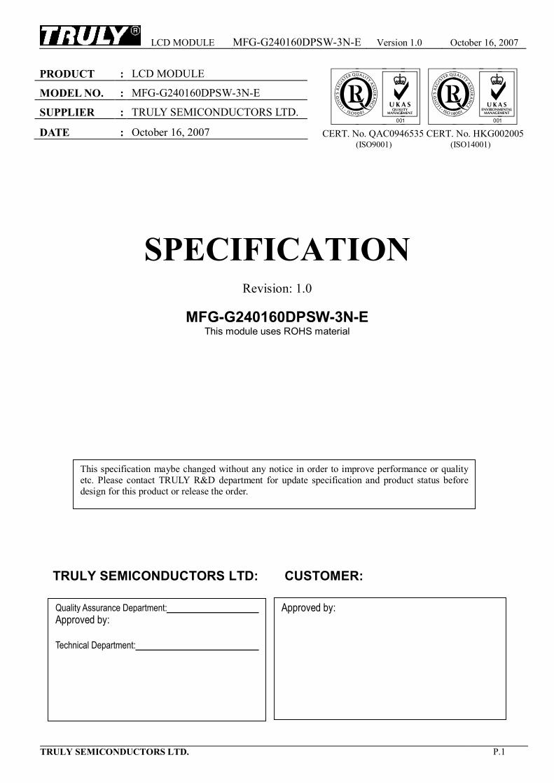
LCD MODULE MFG-G240160DPSW-3N-E Version 1.0 October 16, 2007
TRULY SEMICONDUCTORS LTD. P.1
SPECIFICATION
Revision: 1.0
MFG-G240160DPSW-3N-E This module uses ROHS material
TRULY SEMICONDUCTORS LTD: CUSTOMER:
PRODUCT : LCD MODULE
MODEL NO. : MFG-G240160DPSW-3N-E
SUPPLIER : TRULY SEMICONDUCTORS LTD.
DATE : October 16, 2007 abcdef abcdef CERT. No. QAC0946535 CERT. No. HKG002005
(ISO9001) (ISO14001)
Quality Assurance Department: Approved by: Technical Department:
Approved by:
This specification maybe changed without any notice in order to improve performance or quality etc. Please contact TRULY R&D department for update specification and product status before design for this product or release the order.
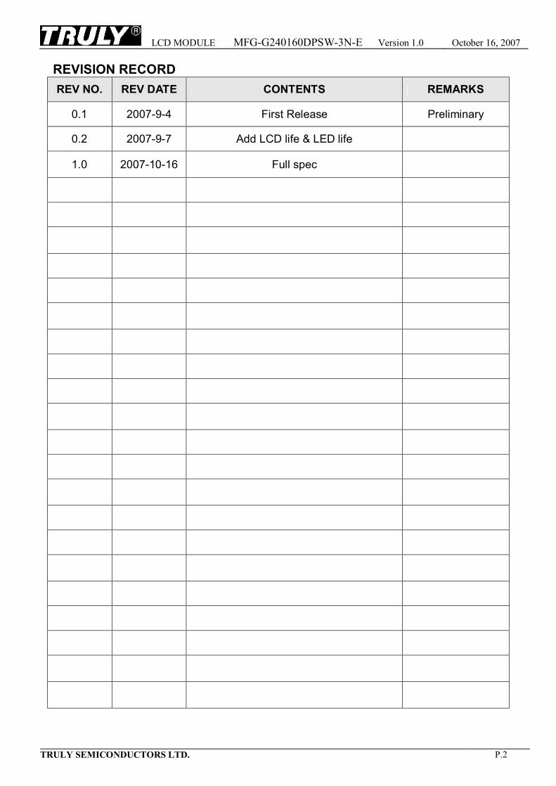
LCD MODULE MFG-G240160DPSW-3N-E Version 1.0 October 16, 2007
TRULY SEMICONDUCTORS LTD. P.2
REVISION RECORD REV NO. REV DATE CONTENTS REMARKS
0.1 2007-9-4 First Release Preliminary
0.2 2007-9-7 Add LCD life & LED life
1.0 2007-10-16 Full spec
LCD MODULE MFG-G240160DPSW-3N-E Version 1.0 October 16, 2007
TRULY SEMICONDUCTORS LTD. P.3
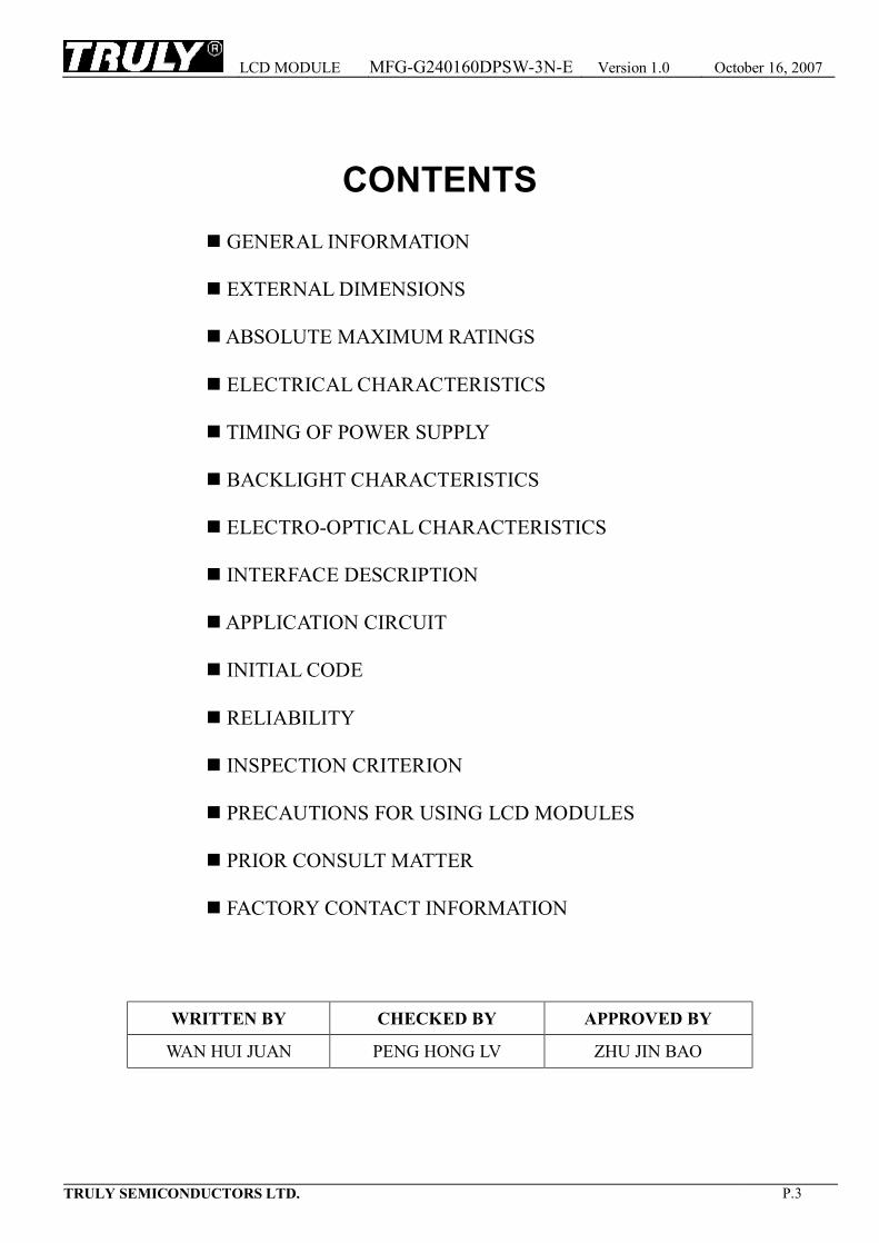
CONTENTS n GENERAL INFORMATION n EXTERNAL DIMENSIONS n ABSOLUTE MAXIMUM RATINGS n ELECTRICAL CHARACTERISTICS n TIMING OF POWER SUPPLY n BACKLIGHT CHARACTERISTICS n ELECTRO-OPTICAL CHARACTERISTICS n INTERFACE DESCRIPTION n APPLICATION CIRCUIT n INITIAL CODE n RELIABILITY n INSPECTION CRITERION n PRECAUTIONS FOR USING LCD MODULES n PRIOR CONSULT MATTER n FACTORY CONTACT INFORMATION
WRITTEN BY CHECKED BY APPROVED BY
WAN HUI JUAN PENG HONG LV ZHU JIN BAO
LCD MODULE MFG-G240160DPSW-3N-E Version 1.0 October 16, 2007
TRULY SEMICONDUCTORS LTD. P.4
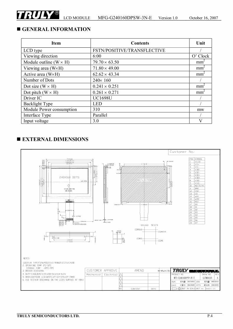
n GENERAL INFORMATION
Item Contents Unit LCD type FSTN/POSITIVE/TRANSFLECTIVE / Viewing direction 6:00 O’ Clock Module outline (W × H) 79.70 × 63.50 mm2 Viewing area (W×H) 71.80 × 49.00 mm2 Active area (W×H) 62.62 × 43.34 mm2 Number of Dots 240× 160 / Dot size (W × H) 0.241 × 0.251 mm2 Dot pitch (W × H) 0.261 × 0.271 mm2 Driver IC UC1698U / Backlight Type LED / Module Power consumption 310 mw Interface Type Parallel / Input voltage 3.0 V
n EXTERNAL DIMENSIONS
1/1
LCD MODULE MFG-G240160DPSW-3N-E Version 1.0 October 16, 2007
TRULY SEMICONDUCTORS LTD. P.5
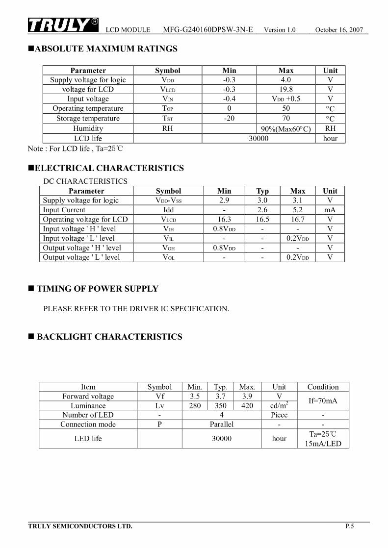
nABSOLUTE MAXIMUM RATINGS
Parameter Symbol Min Max Unit Supply voltage for logic VDD -0.3 4.0 V
voltage for LCD VLCD -0.3 19.8 V Input voltage VIN -0.4 VDD +0.5 V
Operating temperature TOP 0 50 °C Storage temperature TST -20 70 °C
Humidity RH 90%(Max60°C) RH LCD life 30000 hour
Note : For LCD life , Ta=25℃ nELECTRICAL CHARACTERISTICS
DC CHARACTERISTICS Parameter Symbol Min Typ Max Unit
Supply voltage for logic VDD-VSS 2.9 3.0 3.1 V Input Current Idd - 2.6 5.2 mA Operating voltage for LCD VLCD 16.3 16.5 16.7 V Input voltage ' H ' level VIH 0.8VDD - - V Input voltage ' L ' level VIL - - 0.2VDD V Output voltage ' H ' level VOH 0.8VDD - - V Output voltage ' L ' level VOL - - 0.2VDD V
n TIMING OF POWER SUPPLY
PLEASE REFER TO THE DRIVER IC SPECIFICATION. n BACKLIGHT CHARACTERISTICS
Item Symbol Min. Typ. Max. Unit Condition Forward voltage Vf 3.5 3.7 3.9 V
Luminance Lv 280 350 420 cd/m2 If=70mA
Number of LED - 4 Piece - Connection mode P Parallel - -
LED life 30000 hour Ta=25℃ 15mA/LED
LCD MODULE MFG-G240160DPSW-3N-E Version 1.0 October 16, 2007
TRULY SEMICONDUCTORS LTD. P.6
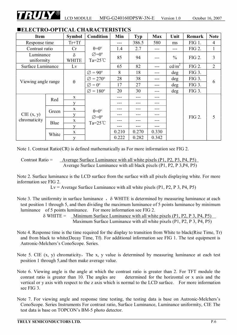
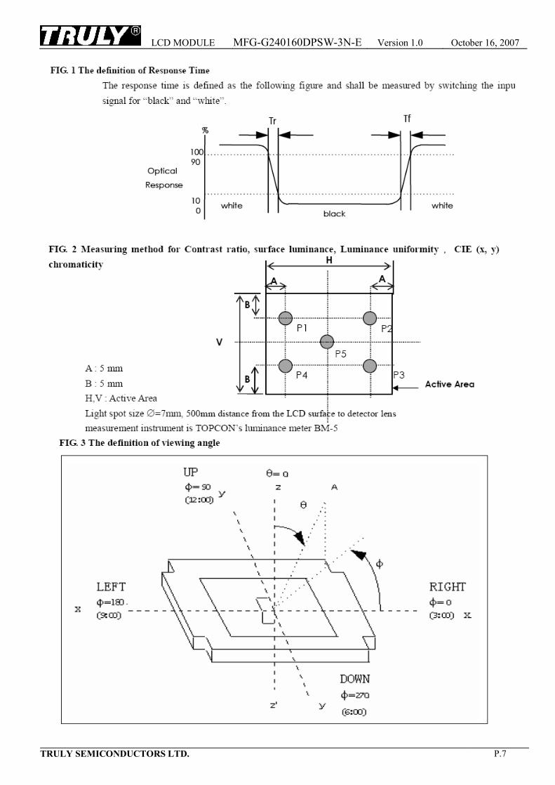
nELECTRO-OPTICAL CHARACTERISTICS Item Symbol Condition Min Typ Max Unit Remark Note
Response time Tr+Tf --- 386.5 580 ms FIG 1. 4 Contrast ratio Cr 1.4 2.7 --- --- FIG 2. 1 Luminance uniformity
δ WHITE 85 94 --- % FIG 2. 3
Surface Luminance Lv
θ=0° ∅=0°
Ta=25℃ 65 82 --- cd/m2 FIG 2. 2
∅ = 90° 8 18 --- deg FIG 3. ∅ = 270° 28 38 --- deg FIG 3. ∅ = 0° 17 27 --- deg FIG 3.
Viewing angle range θ
∅ = 180° 20 30 --- deg FIG 3.
6
x --- --- --- Red y --- --- --- x --- --- --- Green y --- --- --- x --- --- --- Blue y --- --- --- x 0.210 0.270 0.330
CIE (x, y) chromaticity
White y
θ=0° ∅=0°
Ta=25℃
0.222 0.282 0.342
FIG 2. 5
Note 1. Contrast Ratio(CR) is defined mathematically as For more information see FIG 2.
Contrast Ratio = Average Surface Luminance with all white pixels (P1, P2, P3, P4, P5) Average Surface Luminance with all black pixels (P1, P2, P 3,P4, P5)
Note 2. Surface luminance is the LCD surface from the surface with all pixels displaying white. For more information see FIG 2.
Lv = Average Surface Luminance with all white pixels (P1, P2, P 3, P4, P5)
Note 3. The uniformity in surface luminance ,δ WHITE is determined by measuring luminance at each test position 1 through 5, and then dividing the maximum luminance of 5 points luminance by minimum luminance of 5 points luminance. For more information see FIG 2.
δ WHITE = Minimum Surface Luminance with all white pixels (P1, P2, P 3, P4, P5) Maximum Surface Luminance with all white pixels (P1, P2, P 3, P4, P5)
Note 4. Response time is the time required for the display to transition from White to black(Rise Time, Tr) and from black to white(Decay Time, Tf). For additional information see FIG 1. The test equipment is Autronic-Melchers’s ConoScope. Series.
Note 5. CIE (x, y) chromaticity,The x, y value is determined by measuring luminance at each test
position 1 through 5,and then make average value. Note 6. Viewing angle is the angle at which the contrast ratio is greater than 2. For TFT module the
conrast ratio is greater than 10. The angles are determined for the horizontal or x axis and the vertical or y axis with respect to the z axis which is normal to the LCD surface. For more information see FIG 3.
Note 7. For viewing angle and response time testing, the testing data is base on Autronic-Melchers’s
ConoScope. Series Instruments For contrast ratio, Surface Luminance, Luminance uniformity, CIE The test data is base on TOPCON’s BM-5 photo detector.
LCD MODULE MFG-G240160DPSW-3N-E Version 1.0 October 16, 2007
TRULY SEMICONDUCTORS LTD. P.7
LCD MODULE MFG-G240160DPSW-3N-E Version 1.0 October 16, 2007
TRULY SEMICONDUCTORS LTD. P.8
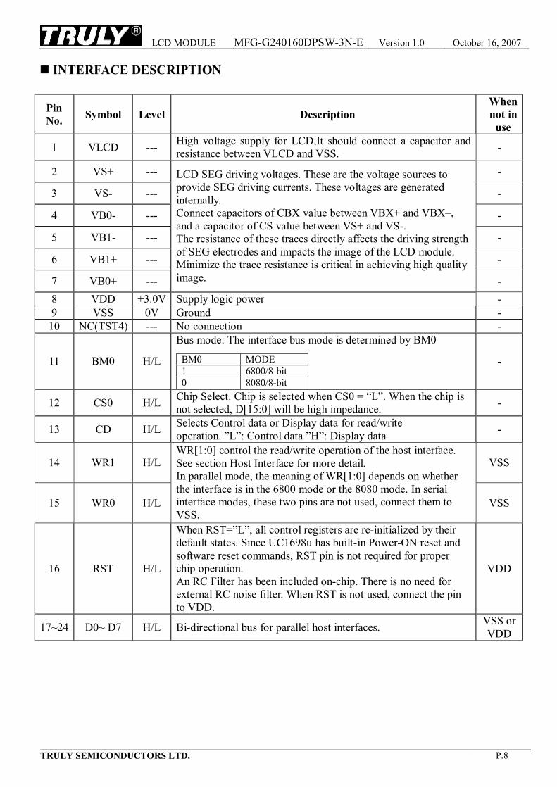
n INTERFACE DESCRIPTION
Pin No. Symbol Level Description
When not in
use
1 VLCD --- High voltage supply for LCD,It should connect a capacitor and resistance between VLCD and VSS. -
2 VS+ --- -
3 VS- --- -
4 VB0- --- -
5 VB1- --- -
6 VB1+ --- -
7 VB0+ ---
LCD SEG driving voltages. These are the voltage sources to provide SEG driving currents. These voltages are generated internally. Connect capacitors of CBX value between VBX+ and VBX–, and a capacitor of CS value between VS+ and VS-. The resistance of these traces directly affects the driving strength of SEG electrodes and impacts the image of the LCD module. Minimize the trace resistance is critical in achieving high quality image. -
8 VDD +3.0V Supply logic power - 9 VSS 0V Ground -
10 NC(TST4) --- No connection -
11 BM0 H/L
Bus mode: The interface bus mode is determined by BM0 BM0 MODE 1 6800/8-bit 0 8080/8-bit
-
12 CS0 H/L Chip Select. Chip is selected when CS0 = “L”. When the chip is not selected, D[15:0] will be high impedance. -
13 CD H/L Selects Control data or Display data for read/write operation. ”L”: Control data ”H”: Display data -
14 WR1 H/L VSS
15 WR0 H/L
WR[1:0] control the read/write operation of the host interface. See section Host Interface for more detail. In parallel mode, the meaning of WR[1:0] depends on whether the interface is in the 6800 mode or the 8080 mode. In serial interface modes, these two pins are not used, connect them to VSS.
VSS
16 RST H/L
When RST=”L”, all control registers are re-initialized by their default states. Since UC1698u has built-in Power-ON reset and software reset commands, RST pin is not required for proper chip operation. An RC Filter has been included on-chip. There is no need for external RC noise filter. When RST is not used, connect the pin to VDD.
VDD
17~24 D0~ D7 H/L Bi-directional bus for parallel host interfaces. VSS or VDD
LCD MODULE MFG-G240160DPSW-3N-E Version 1.0 October 16, 2007
TRULY SEMICONDUCTORS LTD. P.9
n APPLICATION CIRCUIT Please consult our technical department for detail information. n INITIAL CODE Please consult our technical department for detail information. n RELIABILITY
No. Test Item Test Condition Inspection after test 1 High Temperature Storage 70±2℃/240 hours 2 Low Temperature Storage -20±2℃/240 hours 3 High Temperature Operating 50±2℃/240 hours 4 Low Temperature Operating 0±2℃/240 hours
5 Temperature Cycle 0±2℃~25~50±2℃×10cycles (30min.) (5min.) (30min.)
6 Damp Proof Test 50℃±5℃×90%RH/240 hours
7 Vibration Test
Frequency:10Hz~55Hz~10Hz Amplitude:1.5mm, X,Y,Z direction for total 3hours (Packing condition)
8 Drooping test Drop to the ground from 1m height, one time, every side of carton. (Packing condition)
9 ESD test Voltage:±8KV R: 330Ω C: 150pF Air discharge, 10time
Inspection after 2~4hours storage at room temperature, the sample shall be free from defects: 1.Air bubble in the LCD; 2.Sealleak; 3.Non-display; 4.missing segments; 5.Glass crack; 6.Current Idd is twice higher than initial value.
Remark: 1.The test samples should be applied to only one test item. 2.Sample size for each test item is 5~10pcs. 3.For Damp Proof Test, Pure water(Resistance>10MΩ) should be used. 4.In case of malfunction defect caused by ESD damage, if it would be recovered to normal state after resetting, it
would be judge as a good part. Using ionizer(an antistatic blower) is recommended at working area in order to reduce electro-static voltage.
When removing protection film from LCM panel, peel off the tag slowly( recommended more than one second) while blowing with ionizer toward the peeling face to minimize ESD which may damage electrical circuit.
5.EL evaluation should be excepted from reliability test with humidity and temperature: Some defects such as black spot/blemish can happen by natural chemical reaction with humidity and Fluorescence EL has.
6.Please use automatic switch menu(or roll menu) testing mode when test operating mode.
LCD MODULE MFG-G240160DPSW-3N-E Version 1.0 October 16, 2007
TRULY SEMICONDUCTORS LTD. P.10
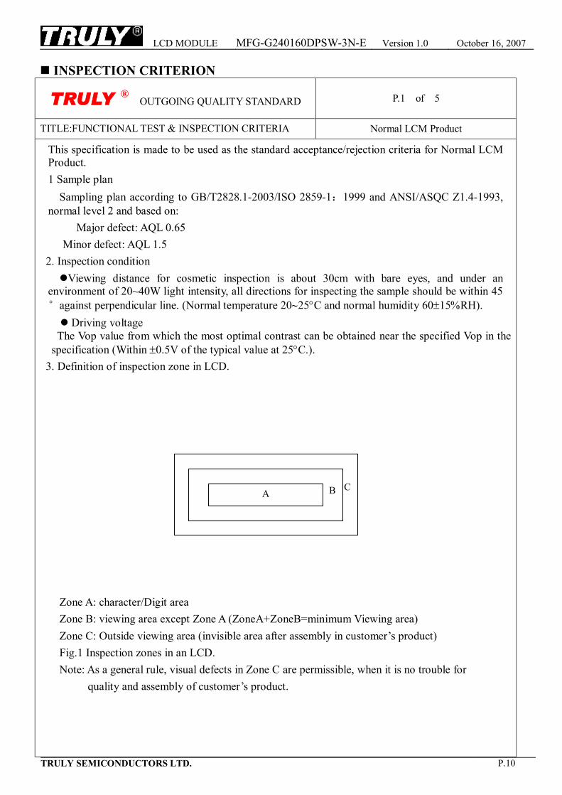
n INSPECTION CRITERION
TRULY ® OUTGOING QUALITY STANDARD P.1 of 5
TITLE:FUNCTIONAL TEST & INSPECTION CRITERIA Normal LCM Product
This specification is made to be used as the standard acceptance/rejection criteria for Normal LCM Product. 1 Sample plan Sampling plan according to GB/T2828.1-2003/ISO 2859-1:1999 and ANSI/ASQC Z1.4-1993, normal level 2 and based on: Major defect: AQL 0.65
Minor defect: AQL 1.5 2. Inspection condition
lViewing distance for cosmetic inspection is about 30cm with bare eyes, and under an environment of 20~40W light intensity, all directions for inspecting the sample should be within 45°against perpendicular line. (Normal temperature 20∼25°C and normal humidity 60±15%RH).
l Driving voltage The Vop value from which the most optimal contrast can be obtained near the specified Vop in the
specification (Within ±0.5V of the typical value at 25°C.). 3. Definition of inspection zone in LCD. Zone A: character/Digit area Zone B: viewing area except Zone A (ZoneA+ZoneB=minimum Viewing area) Zone C: Outside viewing area (invisible area after assembly in customer’s product) Fig.1 Inspection zones in an LCD. Note: As a general rule, visual defects in Zone C are permissible, when it is no trouble for
quality and assembly of customer’s product.
C
B A
LCD MODULE MFG-G240160DPSW-3N-E Version 1.0 October 16, 2007
TRULY SEMICONDUCTORS LTD. P.11
TRULY ® OUTGOING QUALITY STANDARD P.2 of 5
TITLE:FUNCTIONAL TEST & INSPECTION CRITERIA Normal LCM Product
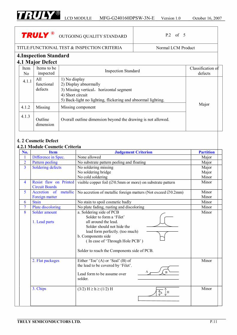
4.Inspection Standard 4.1 Major Defect
Item No
Items to be inspected Inspection Standard Classification of
defects
4.1.1
All functional defects
1) No display 2) Display abnormally 3) Missing vertical,horizontal segment 4) Short circuit 5) Back-light no lighting, flickering and abnormal lighting.
4.1.2 Missing Missing component
4.1.3
Outline dimension
Overall outline dimension beyond the drawing is not allowed.
Major
4.2 Cosmetic Defect 4.2.1 Module Cosmetic Criteria
No. Item Judgement Criterion Partition 1 Difference in Spec. None allowed Major 2 Pattern peeling No substrate pattern peeling and floating Major 3 Soldering defects No soldering missing
No soldering bridge No cold soldering
Major Major Minor
4 Resist flaw on Printed Circuit Boards
visible copper foil (∅0.5mm or more) on substrate pattern Minor
5 Accretion of metallic Foreign matter
No accretion of metallic foreign matters (Not exceed ∅0.2mm) Minor Minor
6 Stain No stain to spoil cosmetic badly Minor 7 Plate discoloring No plate fading, rusting and discoloring Minor 8 Solder amount
1. Lead parts
a. Soldering side of PCB Solder to form a ‘Filet’ all around the lead. Solder should not hide the lead form perfectly. (too much) b. Components side ( In case of ‘Through Hole PCB’ ) Solder to reach the Components side of PCB.
Minor
2. Flat packages Either ‘Toe’ (A) or ‘Seal’ (B) of the lead to be covered by ‘Filet’. Lead form to be assume over solder.
Minor
3. Chips (3/2) H ≥ h ≥ (1/2) H
Minor
H h
A B
LCD MODULE MFG-G240160DPSW-3N-E Version 1.0 October 16, 2007
TRULY SEMICONDUCTORS LTD. P.12
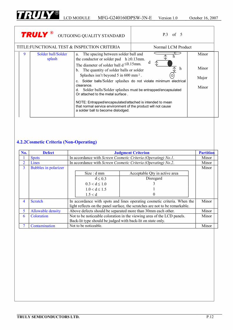
TRULY ® OUTGOING QUALITY STANDARD P.3 of 5
TITLE:FUNCTIONAL TEST & INSPECTION CRITERIA Normal LCM Product 9 Solder ball/Solder
splash a. The spacing between solder ball and the conductor or solder pad h ≥0.13mm. The diameter of solder ball d ≤0.15mm. b. The quantity of solder balls or solder
Splashes isn’t beyond 5 in 600 mm 2 . c. Solder balls/Solder splashes do not violate minimum electrical clearance. d. Solder balls/Solder splashes must be entrapped/encapsulated Or attached to the metal surface . NOTE: Entrapped/encapsulated/attached is intended to mean that normal service environment of the product will not cause a solder ball to become dislodged.
Minor
Minor
Major
Minor
4.2.2Cosmetic Criteria (Non-Operating)
No. Defect Judgment Criterion Partition 1 Spots In accordance with Screen Cosmetic Criteria (Operating) No.1. Minor 2 Lines In accordance with Screen Cosmetic Criteria (Operating) No.2. Minor 3 Bubbles in polarizer
Size : d mm Acceptable Qty in active area d ≤ 0.3 Disregard
0.3 < d ≤ 1.0 3 1.0 < d ≤ 1.5 1 1.5 < d 0
Minor
4 Scratch In accordance with spots and lines operating cosmetic criteria. When the light reflects on the panel surface, the scratches are not to be remarkable.
Minor
5 Allowable density Above defects should be separated more than 30mm each other. Minor 6 Coloration Not to be noticeable coloration in the viewing area of the LCD panels.
Back-lit type should be judged with back-lit on state only. Minor
7 Contamination Not to be noticeable. Minor
h d
h
LCD MODULE MFG-G240160DPSW-3N-E Version 1.0 October 16, 2007
TRULY SEMICONDUCTORS LTD. P.13
TRULY ® OUTGOING QUALITY STANDARD P.4 of 5
TITLE:FUNCTIONAL TEST & INSPECTION CRITERIA Normal LCM Product
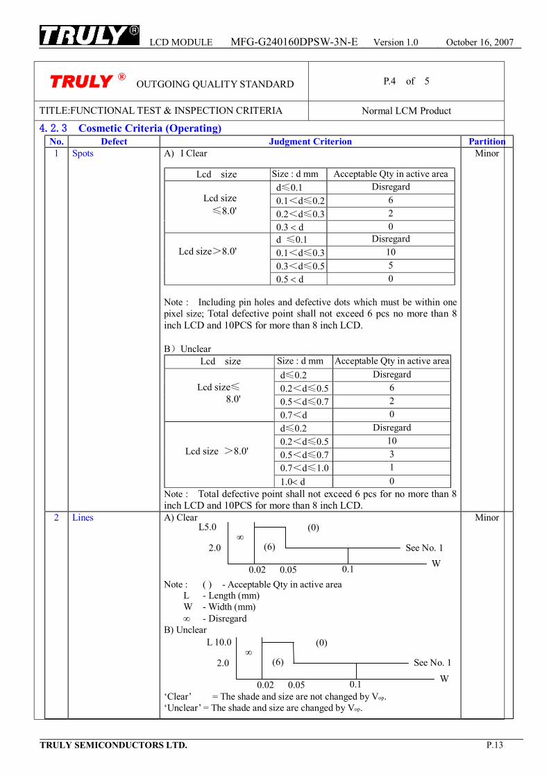
4.2.3 Cosmetic Criteria (Operating) No. Defect Judgment Criterion Partition 1 Spots A) I Clear
Note : Including pin holes and defective dots which must be within one pixel size; Total defective point shall not exceed 6 pcs no more than 8 inch LCD and 10PCS for more than 8 inch LCD. B) Unclear
Lcd size Size : d mm Acceptable Qty in active area d≤0.2 Disregard 0.2<d≤0.5 6 0.5<d≤0.7 2
Lcd size≤
8.0' 0.7<d 0 d≤0.2 Disregard 0.2<d≤0.5 10 0.5<d≤0.7 3 0.7<d≤1.0 1
Lcd size >8.0'
1.0< d 0 Note : Total defective point shall not exceed 6 pcs for no more than 8 inch LCD and 10PCS for more than 8 inch LCD.
Lcd size Size : d mm Acceptable Qty in active area d≤0.1 Disregard 0.1<d≤0.2 6 0.2<d≤0.3 2
Lcd size
≤8.0' 0.3 < d 0 d ≤0.1 Disregard 0.1<d≤0.3 10 0.3<d≤0.5 5
Lcd size>8.0'
0.5 < d 0
Minor
2 Lines A) Clear Note : ( ) - Acceptable Qty in active area L - Length (mm) W - Width (mm) ∞ - Disregard B) Unclear ‘Clear’ = The shade and size are not changed by Vop. ‘Unclear’ = The shade and size are changed by Vop.
Minor
2.0
L 10.0
See No. 1 ∞
(6)
(0)
W 0.1 0.05 0.02
2.0
L5.0
See No. 1 ∞
(6)
(0)
W 0.1 0.05 0.02
LCD MODULE MFG-G240160DPSW-3N-E Version 1.0 October 16, 2007
TRULY SEMICONDUCTORS LTD. P.14
TRULY ® OUTGOING QUALITY STANDARD P.5 of 5
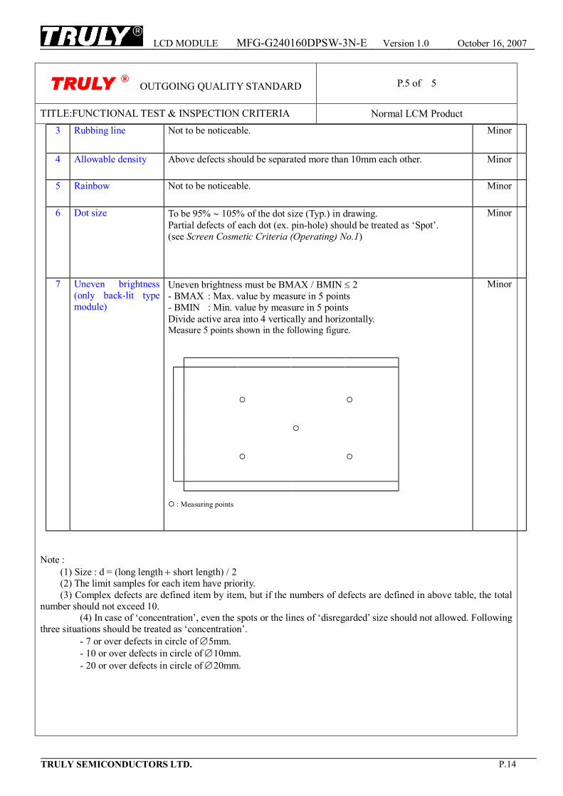
TITLE:FUNCTIONAL TEST & INSPECTION CRITERIA Normal LCM Product 3 Rubbing line Not to be noticeable. Minor
4 Allowable density Above defects should be separated more than 10mm each other. Minor
5 Rainbow Not to be noticeable. Minor
6 Dot size To be 95% ∼ 105% of the dot size (Typ.) in drawing. Partial defects of each dot (ex. pin-hole) should be treated as ‘Spot’. (see Screen Cosmetic Criteria (Operating) No.1)
Minor
7 Uneven brightness (only back-lit type module)
Uneven brightness must be BMAX / BMIN ≤ 2 - BMAX : Max. value by measure in 5 points - BMIN : Min. value by measure in 5 points Divide active area into 4 vertically and horizontally. Measure 5 points shown in the following figure.
¡ ¡
¡
¡ ¡
¡ : Measuring points
Minor
Note : (1) Size : d = (long length + short length) / 2 (2) The limit samples for each item have priority. (3) Complex defects are defined item by item, but if the numbers of defects are defined in above table, the total number should not exceed 10. (4) In case of ‘concentration’, even the spots or the lines of ‘disregarded’ size should not allowed. Following three situations should be treated as ‘concentration’. - 7 or over defects in circle of ∅5mm. - 10 or over defects in circle of ∅10mm. - 20 or over defects in circle of ∅20mm.
LCD MODULE MFG-G240160DPSW-3N-E Version 1.0 October 16, 2007
TRULY SEMICONDUCTORS LTD. P.15
n PRECAUTIONS FOR USING LCD MODULES Handing Precautions (1) The display panel is made of glass and polarizer. As glass is fragile. It tends to become or chipped during handling especially on the edges. Please avoid dropping or jarring. Do not subject it to a mechanical shock by dropping it or impact. (2) If the display panel is damaged and the liquid crystal substance leaks out, be sure not to get any in your mouth. If the substance contacts your skin or clothes, wash it off using soap and water. (3) Do not apply excessive force to the display surface or the adjoining areas since this may cause the color tone to vary. Do not touch the display with bare hands. This will stain the display area and degraded insulation between terminals (some cosmetics are determined to the polarizer). (4) The polarizer covering the display surface of the LCD module is soft and easily scratched. Handle this polarizer carefully. Do not touch, push or rub the exposed polarizers with anything harder than an HB pencil lead (glass, tweezers, etc.). Do not put or attach anything on the display area to avoid leaving marks on. Condensation on the surface and contact with terminals due to cold will damage, stain or dirty the polarizer. After products are tested at low temperature they must be warmed up in a container before coming is contacting with room temperature air. (5) If the display surface becomes contaminated, breathe on the surface and gently wipe it with a soft dry cloth. If it is heavily contaminated, moisten cloth with one of the following solvents - Isopropyl alcohol - Ethyl alcohol Do not scrub hard to avoid damaging the display surface. (6) Solvents other than those above-mentioned may damage the polarizer. Especially, do not use the following. - Water - Ketone - Aromatic solvents Wipe off saliva or water drops immediately, contact with water over a long period of time may cause deformation or color fading. Avoid contacting oil and fats. (7) Exercise care to minimize corrosion of the electrode. Corrosion of the electrodes is accelerated by water droplets, moisture condensation or a current flow in a high-humidity environment. (8) Install the LCD Module by using the mounting holes. When mounting the LCD module make sure it is free of twisting, warping and distortion. In particular, do not forcibly pull or bend the I/O cable or the backlight cable. (9) Do not attempt to disassemble or process the LCD module. (10) NC terminal should be open. Do not connect anything. (11) If the logic circuit power is off, do not apply the input signals. (12) Electro-Static Discharge Control,Since this module uses a CMOS LSI, the same careful attention should be paid to electrostatic discharge as for an ordinary CMOS IC. To prevent destruction of the elements by static electricity, be careful to maintain an optimum work environment. - Before remove LCM from its packing case or incorporating it into a set, be sure the module and your body have the same electric potential. Be sure to ground the body when handling the LCD modules. - Tools required for assembling, such as soldering irons, must be properly grounded. make certain the AC power source for the soldering iron does not leak. When using an electric screwdriver to attach LCM, the screwdriver should be of ground potentiality to minimize as much as possible any transmission of electromagnetic waves produced sparks coming from the commutator of the motor. - To reduce the amount of static electricity generated, do not conduct assembling and other work under dry conditions. To reduce the generation of static electricity be careful that the air in the work is not too dried. A relative humidity of 50%-60% is recommended. As far as possible make the electric potential of your work clothes and that of the work bench the ground potential - The LCD module is coated with a film to protect the display surface. Exercise care when peeling off this protective film since static electricity may be generated
LCD MODULE MFG-G240160DPSW-3N-E Version 1.0 October 16, 2007
TRULY SEMICONDUCTORS LTD. P.16
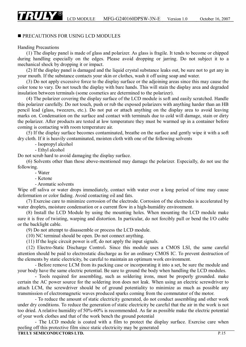
(13)Since LCM has been assembled and adjusted with a high degree of precision, avoid applying excessive shocks to the module or making any alterations or modifications to it. - Do not alter, modify or change the shape of the tab on the metal frame. - Do not make extra holes on the printed circuit board, modify its shape or change the positions of components to be attached. - Do not damage or modify the pattern writing on the printed circuit board. - Absolutely do not modify the zebra rubber strip (conductive rubber) or heat seal connector. - Except for soldering the interface, do not make any alterations or modifications with a soldering iron. - Do not drop, bend or twist LCM. Handling precaution for LCM
LCD MODULE MFG-G240160DPSW-3N-E Version 1.0 October 16, 2007
TRULY SEMICONDUCTORS LTD. P.17
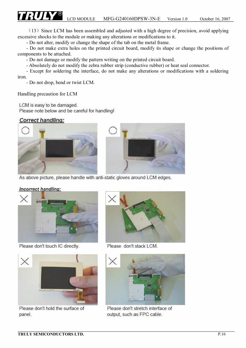
Handling precaution for LCD
LCD MODULE MFG-G240160DPSW-3N-E Version 1.0 October 16, 2007
TRULY SEMICONDUCTORS LTD. P.18
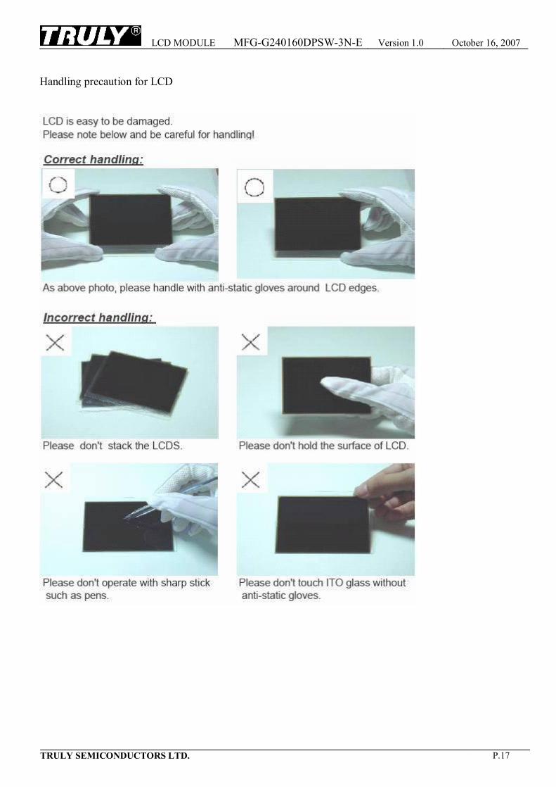
Storage Precautions When storing the LCD modules, the following precaution is necessary. (1) Store them in a sealed polyethylene bag. If properly sealed, there is no need for the dessicant. (2) Store them in a dark place. Do not expose to sunlight or fluorescent light, keep the temperature between 0°C and 35°C, and keep the relative humidity between 40%RH and 60%RH. (3) The polarizer surface should not come in contact with any other objects. (We advise you to store them in the anti-static electricity container in which they were shipped. Others Liquid crystals solidify under low temperature (below the storage temperature range) leading to defective orientation or the generation of air bubbles (black or white). Air bubbles may also be generated if the module is subject to a low temperature. If the LCD modules have been operating for a long time showing the same display patterns, the display patterns may remain on the screen as ghost images and a slight contrast irregularity may also appear. A normal operating status can be regained by suspending use for some time. It should be noted that this phenomenon does not adversely affect performance reliability. To minimize the performance degradation of the LCD modules resulting from destruction caused by static electricity etc., exercise care to avoid holding the following sections when handling the modules. - Exposed area of the printed circuit board. -Terminal electrode sections. n USING LCD MODULES Installing LCD Modules The hole in the printed circuit board is used to fix LCM as shown in the picture below. Attend to the following items when installing the LCM. (1) Cover the surface with a transparent protective plate to protect the polarizer and LC cell.
(2) When assembling the LCM into other equipment, the spacer to the bit between the LCM and the fitting plate should have enough height to avoid causing stress to the module surface, refer to the individual specifications for measurements. The measurement tolerance should be ±0.1mm. Precaution for assemble the module with BTB connector: Please note the position of the male and female connector position, don’t assemble or assemble like the method which the following picture shows
LCD MODULE MFG-G240160DPSW-3N-E Version 1.0 October 16, 2007
TRULY SEMICONDUCTORS LTD. P.19
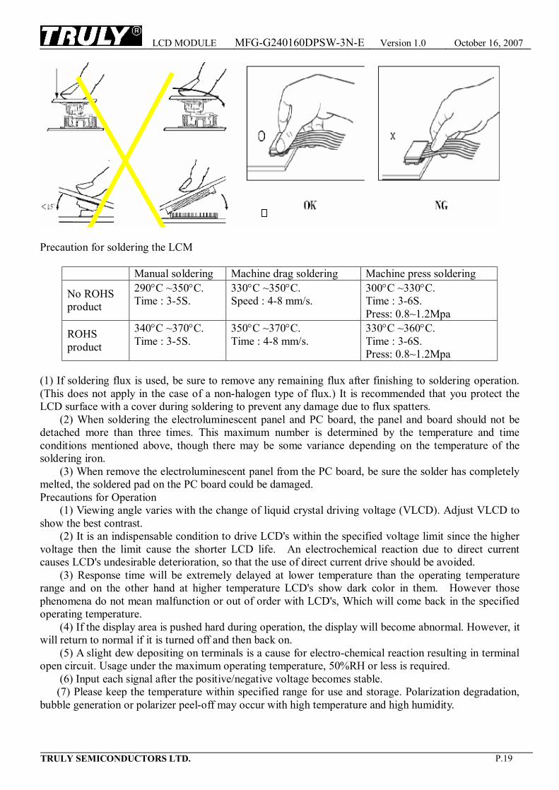
Precaution for soldering the LCM
Manual soldering Machine drag soldering Machine press soldering
No ROHS product
290°C ~350°C. Time : 3-5S.
330°C ~350°C. Speed : 4-8 mm/s.
300°C ~330°C. Time : 3-6S. Press: 0.8~1.2Mpa
ROHS product
340°C ~370°C. Time : 3-5S.
350°C ~370°C. Time : 4-8 mm/s.
330°C ~360°C. Time : 3-6S. Press: 0.8~1.2Mpa
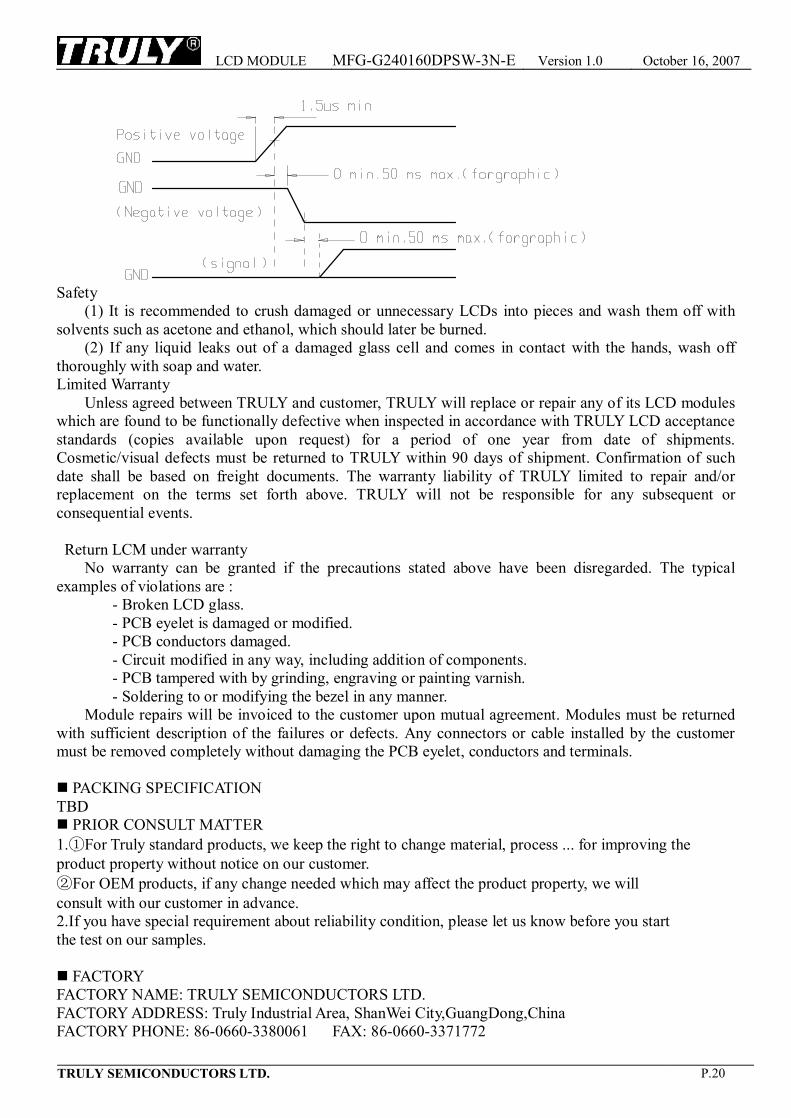
(1) If soldering flux is used, be sure to remove any remaining flux after finishing to soldering operation. (This does not apply in the case of a non-halogen type of flux.) It is recommended that you protect the LCD surface with a cover during soldering to prevent any damage due to flux spatters. (2) When soldering the electroluminescent panel and PC board, the panel and board should not be detached more than three times. This maximum number is determined by the temperature and time conditions mentioned above, though there may be some variance depending on the temperature of the soldering iron. (3) When remove the electroluminescent panel from the PC board, be sure the solder has completely melted, the soldered pad on the PC board could be damaged. Precautions for Operation (1) Viewing angle varies with the change of liquid crystal driving voltage (VLCD). Adjust VLCD to show the best contrast. (2) It is an indispensable condition to drive LCD's within the specified voltage limit since the higher voltage then the limit cause the shorter LCD life. An electrochemical reaction due to direct current causes LCD's undesirable deterioration, so that the use of direct current drive should be avoided. (3) Response time will be extremely delayed at lower temperature than the operating temperature range and on the other hand at higher temperature LCD's show dark color in them. However those phenomena do not mean malfunction or out of order with LCD's, Which will come back in the specified operating temperature. (4) If the display area is pushed hard during operation, the display will become abnormal. However, it will return to normal if it is turned off and then back on. (5) A slight dew depositing on terminals is a cause for electro-chemical reaction resulting in terminal open circuit. Usage under the maximum operating temperature, 50%RH or less is required. (6) Input each signal after the positive/negative voltage becomes stable. (7) Please keep the temperature within specified range for use and storage. Polarization degradation, bubble generation or polarizer peel-off may occur with high temperature and high humidity.
LCD MODULE MFG-G240160DPSW-3N-E Version 1.0 October 16, 2007
TRULY SEMICONDUCTORS LTD. P.20
Safety (1) It is recommended to crush damaged or unnecessary LCDs into pieces and wash them off with solvents such as acetone and ethanol, which should later be burned. (2) If any liquid leaks out of a damaged glass cell and comes in contact with the hands, wash off thoroughly with soap and water. Limited Warranty Unless agreed between TRULY and customer, TRULY will replace or repair any of its LCD modules which are found to be functionally defective when inspected in accordance with TRULY LCD acceptance standards (copies available upon request) for a period of one year from date of shipments. Cosmetic/visual defects must be returned to TRULY within 90 days of shipment. Confirmation of such date shall be based on freight documents. The warranty liability of TRULY limited to repair and/or replacement on the terms set forth above. TRULY will not be responsible for any subsequent or consequential events. Return LCM under warranty No warranty can be granted if the precautions stated above have been disregarded. The typical examples of violations are : - Broken LCD glass. - PCB eyelet is damaged or modified. - PCB conductors damaged. - Circuit modified in any way, including addition of components. - PCB tampered with by grinding, engraving or painting varnish. - Soldering to or modifying the bezel in any manner. Module repairs will be invoiced to the customer upon mutual agreement. Modules must be returned with sufficient description of the failures or defects. Any connectors or cable installed by the customer must be removed completely without damaging the PCB eyelet, conductors and terminals. n PACKING SPECIFICATION TBD n PRIOR CONSULT MATTER 1.①For Truly standard products, we keep the right to change material, process ... for improving the product property without notice on our customer. ②For OEM products, if any change needed which may affect the product property, we will consult with our customer in advance. 2.If you have special requirement about reliability condition, please let us know before you start the test on our samples. n FACTORY FACTORY NAME: TRULY SEMICONDUCTORS LTD. FACTORY ADDRESS: Truly Industrial Area, ShanWei City,GuangDong,China FACTORY PHONE: 86-0660-3380061 FAX: 86-0660-3371772


![abcdef · 2015-06-03 · abcdef ˘ˇˆ˙˝˛˚˜ !" #$%$&’( )*˛+,-./01 2341’5 6 7839: ;? @ABC. DEBFGHIJKLM NO PQ0 R ˘ S4$41’ abcdef TUV S˘GW41 ˛XYZ[\=] ^3BC. ˛_‘](https://img.dokumen.tips/doc/110x75/5f8c828efac1f36a415478c1/abcdef-2015-06-03-abcdef-oe-a-01-2341a5.jpg)
![! #$ 89:-.;?@ABCDEF!G.$%HIJKL*+,-./0,123456789 :;?@ABCDEF)GHIJKL >0,1MNOPQRSTU*+,-.VWXYZ>*+[0\].>^_E‘a)G bIJcdW*+,-.eZE fghijklmn:;op qrstuvwxyzE!""#{9|}~pp](https://img.dokumen.tips/doc/110x75/60477cab9faf676b8110cfd7/-89-abcdefg-0123456789-abcdefghijkl-01mnopqrstu-vwxyz0eaag.jpg)


![[14.12.02] ABCDEF](https://img.dokumen.tips/doc/110x75/55978f6f1a28abd0368b4750/141202-abcdef.jpg)