Embed Size (px)
DESCRIPTION
presentation file for Embedded systems prepared for PG power electronics students
Citation preview

ARCHITECTURAL OVERVIEW OF PIC16FXX

ARCHITECTURAL OVERVIEW OF PIC16FXX• Harvard architecture: the program and data accessed from separate memories. So
the device has a program memory bus and a data memory bus. This improves bandwidth over traditional von Neumann architecture where program and data are fetched from the same memory (accesses over the same bus). Separating program and data memory further allows instructions to be sized differently than the 8-bit wide data word.
A two-stage pipeline overlaps fetch and execution of instructions Consequently, all instructions execute in a single cycle (400 ns @ 10 MHz) except for program branches.


ARCHITECTURAL OVERVIEW OF PIC16FXX
The ALU is 8-bits wide and capable of addition, subtraction, shift and logical operations.

ARCHITECTURAL OVERVIEW OF PIC16FXX
• The program memory and the data memory block has its own bus, so that access to each block can occur during the same oscillator cycle.•The data memory can further be broken down into the general purpose RAM and the Special Function Registers (SFRs). •The SFRs used to control the peripheral modules
• Memory Organization

ARCHITECTURAL OVERVIEW OF PIC16FXX
Program Memory
13-bit program counter capable of addressing program memory

ARCHITECTURAL OVERVIEW OF PIC16FXX
• Data Memory OrganizationTwo areas, the first is the Special Function Registers (SFR) area, while the second is the General Purpose Registers (GPR) area.The SFRs control the operation of the device.

ARCHITECTURAL OVERVIEW OF PIC16FXX

REGISTERs• INTCON REGISTER The INTCON register is a readable and writable register which
contains the various enable bits for all interrupt sources.

REGISTERs• Program Counter: PCL and PCLATHThe Program Counter (PC) is 13-bits widePCL register, which is a readable and writable registerThe high byte of the PC (PC<12:8>) is not directly readable nor
writable and comes from the PCLATH registerThe PCLATH (PC latch high) register is a holding register for
PC<12:8>. • PCLATH are transferred to the upper byte of the program
counter when CALL, GOTO or a write to PCL.

REGISTERs

REGISTERs• Stack The PIC16FXX has an 8 deep x 13-bit wide
hardware stack The stack space is not part of either program or data space and the stack pointer is not readable or writable.
• The entire 13-bit PC is “pushed” onto the stack when a CALL instruction is executed or an interrupt is acknowledged.
• The stack is “popped” in the event of a RETURN, RETLW or a RETFIE instruction execution.

REGISTERs
• Indirect Addressing; INDF and FSR Registers The INDF register is not a physical register.
Addressing INDF actually addresses the register whose address is contained in the FSR register (FSR is a pointer). This is indirect addressing.

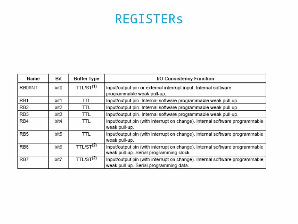
REGISTERs• I/O PORTS All the pins of Port A have data direction bits (TRIS registers)
which can configure these pins as output or input Setting a TRISA bit (=1) will make the corresponding PORT A pin an input Clearing a TRISA bit (=0) will make the corresponding PORT
A pin an output

REGISTERs• PORTB and TRISB Registers• PORTB is an 8-bit wide bi-directional port. • The corresponding data direction register is TRISB. A
'1' on any bit in the TRISB register puts the corresponding output driver in a hi-impedance mode. A '0' on any bit in the TRISB register puts the contents of the output latch on the selected pin(s).
REGISTERs

REGISTERs
• TIMER0 MODULE AND TMR0 REGISTER• The Timer0 module timer/counter has the followingfeatures: 8-bit timer/counter•Readable and writable 8-bit software programmable prescalerInternal or external clock select Interrupt on overflow from FFh to 00h Edge select for external clock

REGISTERs• Timer mode is selected by clearing the T0CS bit
(OPTION<5>). In timer mode, the Timer0 module will increment every instruction cycle (without pre-saler)
• Counter mode is selected by setting the T0CS bit (OPTION<5>) In this mode TMR0 will increment either
• on every rising or falling edge of pin RA4/T0CKI. The incrementing edge is determined by the T0 source edge select bit, T0SE (OPTION<4>). Clearing bit T0SE
selects the rising edge.

REGISTERs• The prescaler is shared between the Timer0
Module and the Watchdog Timer.
The TMR0 interrupt is generated when the TMR0 register overflows from FFh to 00h. This overflow sets the T0IF bit (INTCON<2>).

REGISTERs• Using TMR0 with External Clock• When an external clock input is used for TMR0, it
must meet certain requirements. • The external clock requirement is due to internal
phase clock (TOSC)synchronization. Also, there is a delay in the actual incrementing of the TMR0 register after synchronization

REGISTERs
• An 8-bit counter is available as a prescaler for the Timer0 Module, or as a postscaler for the Watchdog Timer


![[2]Associate Professor, Department of EEE Krishnasamy ... › research › a-novel-integrated...J.Sheela Arokia Mary[1],S.Sivasakthi[2] [1]Student, M.E. Embedded System Technologies](https://img.dokumen.tips/doc/110x75/60cef79ec3678218c75e9394/2associate-professor-department-of-eee-krishnasamy-a-research-a-a-novel-integrated.jpg)


![Question Papers/R13/ME/MA7163/MA7163... · MM 163 -APPLIED MATHEMATICS FOR ELECTRICAL ENGINEERS (Common to M.E. Electrical Drives and Embedded Control]M.E. Embedded System Technologies/M.E](https://img.dokumen.tips/doc/110x75/5e7b33f31d740328276adb23/question-papersr13mema7163ma7163-mm-163-applied-mathematics-for-electrical.jpg)