Embed Size (px)
Citation preview
MCP4802/4812/48228/10/12-Bit Dual Voltage Output Digital-to-Analog Converter
with Internal VREF and SPI Interface
Features• MCP4802: Dual 8-Bit Voltage Output DAC• MCP4812: Dual 10-Bit Voltage Output DAC• MCP4822: Dual 12-Bit Voltage Output DAC• Rail-to-Rail Output• SPI Interface with 20 MHz Clock Support• Simultaneous Latching of the Dual DACs
with LDAC pin• Fast Settling Time of 4.5 µs• Selectable Unity or 2x Gain Output• 2.048V Internal Voltage Reference• 50 ppm/°C VREF Temperature Coefficient• 2.7V to 5.5V Single-Supply Operation• Extended Temperature Range: -40°C to +125°C
Applications• Set Point or Offset Trimming• Sensor Calibration• Precision Selectable Voltage Reference• Portable Instrumentation (Battery-Powered)• Calibration of Optical Communication Devices
DescriptionThe MCP4802/4812/4822 devices are dual 8-bit, 10-bitand 12-bit buffered voltage output Digital-to-AnalogConverters (DACs), respectively. The devices operatefrom a single 2.7V to 5.5V supply with SPI compatibleSerial Peripheral Interface. The devices have a high precision internal voltagereference (VREF = 2.048V). The user can configure thefull-scale range of the device to be 2.048V or 4.096V bysetting the Gain Selection Option bit (gain of 1 of 2).Each DAC channel can be operated in Active orShutdown mode individually by setting the Configurationregister bits. In Shutdown mode, most of the internalcircuits in the shutdown channel are turned off for powersavings and the output amplifier is configured to presenta known high resistance output load (500 k typical. The devices include double-buffered registers,allowing synchronous updates of two DAC outputsusing the LDAC pin. These devices also incorporate aPower-on Reset (POR) circuit to ensure reliable power-up.The devices utilize a resistive string architecture, withits inherent advantages of low DNL error, low ratiometric temperature coefficient and fast settling time.These devices are specified over the extendedtemperature range (+125°C). The devices provide high accuracy and low noiseperformance for consumer and industrial applicationswhere calibration or compensation of signals (such astemperature, pressure and humidity) are required. The MCP4802/4812/4822 devices are available in thePDIP, SOIC and MSOP packages.
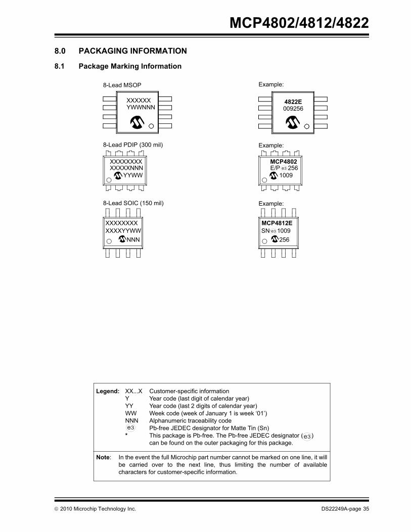
Package Types
Related Products(1)
P/N DAC Resolution
No. of Channels
Voltage Reference
(VREF)
MCP4801 8 1
Internal(2.048V)
MCP4811 10 1MCP4821 12 1MCP4802 8 2MCP4812 10 2MCP4822 12 2MCP4901 8 1
External
MCP4911 10 1MCP4921 12 1MCP4902 8 2MCP4912 10 2MCP4922 12 2
Note 1: The products listed here have similarAC/DC performances.
MC
P48X
2
8-Pin PDIP, SOIC, MSOP
1
2
3
4
8
7
6
5
CS
SCK
SDI
VDD
VSS
VOUTA
VOUTB
LDAC
MCP4802: 8-bit dual DACMCP4812: 10-bit dual DACMCP4822: 12-bit dual DAC
2010 Microchip Technology Inc. DS22249A-page 1
MCP4802/4812/4822
Block DiagramOp Amps
VDD
VSS
CS SDI SCK
Interface Logic
Input Register A Register B
Input
DACA Register Register
DACB
StringDACB
StringDACA
Output
Power-on Reset
VOUTA VOUTB
LDAC
OutputGainLogic
GainLogic
2.048VVREF
Logic
DS22249A-page 2 2010 Microchip Technology Inc.
MCP4802/4812/4822
1.0 ELECTRICAL CHARACTERISTICS
Absolute Maximum Ratings †VDD....................................................................... 6.5V
All inputs and outputs .......... VSS – 0.3V to VDD + 0.3V Current at Input Pins ......................................... ±2 mACurrent at Supply Pins .................................... ±50 mACurrent at Output Pins .................................... ±25 mAStorage temperature .......................... -65°C to +150°CAmbient temp. with power applied ..... -55°C to +125°CESD protection on all pins 4 kV (HBM), 400V (MM)Maximum Junction Temperature (TJ)................+150°C
† Notice: Stresses above those listed under “MaximumRatings” may cause permanent damage to the device.This is a stress rating only and functional operation ofthe device at those or any other conditions above thoseindicated in the operational listings of this specificationis not implied. Exposure to maximum rating conditionsfor extended periods may affect device reliability.
ELECTRICAL CHARACTERISTICSElectrical Specifications: Unless otherwise indicated, VDD = 5V, VSS = 0V, VREF = 2.048V, Output Buffer Gain (G) = 2x, RL = 5 k to GND, CL = 100 pF, TA = -40 to +85°C. Typical values are at +25°C.
Parameters Sym Min Typ Max Units Conditions
Power RequirementsInput Voltage VDD 2.7 — 5.5 VInput Current IDD — 415 750 µA All digital inputs are grounded,
all analog outputs (VOUT) are unloaded. Code = 0x000h
Software Shutdown Current ISHDN_SW — 3.3 6 µAPower-on Reset Threshold VPOR — 2.0 — VDC AccuracyMCP4802
Resolution n 8 — — BitsINL Error INL -1 ±0.125 1 LSbDNL DNL -0.5 ±0.1 +0.5 LSb Note 1
MCP4812Resolution n 10 — — BitsINL Error INL -3.5 ±0.5 3.5 LSbDNL DNL -0.5 ±0.1 +0.5 LSb Note 1
MCP4822Resolution n 12 — — BitsINL Error INL -12 ±2 12 LSbDNL DNL -0.75 ±0.2 +0.75 LSb Note 1
Offset Error VOS -1 ±0.02 1 % of FSR Code = 0x000hOffset Error TemperatureCoefficient
VOS/°C — 0.16 — ppm/°C -45°C to +25°C— -0.44 — ppm/°C +25°C to +85°C
Gain Error gE -2 -0.10 2 % of FSR Code = 0xFFFh, not including offset error
Gain Error Temperature Coefficient
G/°C — -3 — ppm/°C
Note 1: Guaranteed monotonic by design over all codes.2: This parameter is ensured by design, and not 100% tested.
2010 Microchip Technology Inc. DS22249A-page 3
MCP4802/4812/4822
Internal Voltage Reference (VREF)Internal Reference Voltage VREF 2.008 2.048 2.088 V VOUTA when G = 1x and
Code = 0xFFFhTemperature Coefficient(Note 2)
VREF/°C — 125 325 ppm/°C -40°C to 0°C— 0.25 0.65 LSb/°C -40°C to 0°C— 45 160 ppm/°C 0°C to +85°C— 0.09 0.32 LSb/°C 0°C to +85°C
Output Noise (VREF Noise) ENREF(0.1-
10 Hz)
— 290 — µVp-p Code = 0xFFFh, G = 1x
Output Noise Density eNREF(1 kHz)
— 1.2 — µV/Hz Code = 0xFFFh, G = 1x
eNREF(10 kHz)
— 1.0 — µV/Hz Code = 0xFFFh, G = 1x
1/f Corner Frequency fCORNER — 400 — HzOutput AmplifierOutput Swing VOUT — 0.01 to
VDD – 0.04 — V Accuracy is better than 1 LSb for
VOUT = 10 mV to (VDD–40 mV)Phase Margin PM — 66 — Degree
(°)CL= 400 pF, RL =
Slew Rate SR — 0.55 — V/µsShort Circuit Current ISC — 15 24 mASettling Time tSETTLING — 4.5 — µs Within 1/2 LSb of final value from
1/4 to 3/4 full-scale rangeDynamic Performance (Note 2)DAC-to-DAC Crosstalk — <10 — nV-sMajor Code Transition Glitch — 45 — nV-s 1 LSb change around major carry
(0111...1111 to 1000...0000)
Digital Feedthrough — <10 — nV-sAnalog Crosstalk — <10 — nV-s
ELECTRICAL CHARACTERISTICS (CONTINUED)Electrical Specifications: Unless otherwise indicated, VDD = 5V, VSS = 0V, VREF = 2.048V, Output Buffer Gain (G) = 2x, RL = 5 k to GND, CL = 100 pF, TA = -40 to +85°C. Typical values are at +25°C.
Parameters Sym Min Typ Max Units Conditions
Note 1: Guaranteed monotonic by design over all codes.2: This parameter is ensured by design, and not 100% tested.
DS22249A-page 4 2010 Microchip Technology Inc.
MCP4802/4812/4822
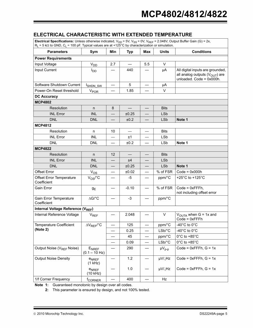
ELECTRICAL CHARACTERISTIC WITH EXTENDED TEMPERATUREElectrical Specifications: Unless otherwise indicated, VDD = 5V, VSS = 0V, VREF = 2.048V, Output Buffer Gain (G) = 2x, RL = 5 k to GND, CL = 100 pF. Typical values are at +125°C by characterization or simulation.
Parameters Sym Min Typ Max Units Conditions
Power RequirementsInput Voltage VDD 2.7 — 5.5 VInput Current Input Curren
IDD — 440 — µA All digital inputs are grounded, all analog outputs (VOUT) are unloaded. Code = 0x000h.
Software Shutdown Current ISHDN_SW — 5 — µAPower-On Reset threshold VPOR — 1.85 — VDC AccuracyMCP4802
Resolution n 8 — — BitsINL Error INL — ±0.25 — LSb DNL DNL — ±0.2 — LSb Note 1
MCP4812Resolution n 10 — — BitsINL Error INL — ±1 — LSb DNL DNL — ±0.2 — LSb Note 1
MCP4822Resolution n 12 — — BitsINL Error INL — ±4 — LSb DNL DNL — ±0.25 — LSb Note 1
Offset Error VOS — ±0.02 — % of FSR Code = 0x000hOffset Error TemperatureCoefficient
VOS/°C — -5 — ppm/°C +25°C to +125°C
Gain Error gE — -0.10 — % of FSR Code = 0xFFFh, not including offset error
Gain Error Temperature Coefficient
G/°C — -3 — ppm/°C
Internal Voltage Reference (VREF)Internal Reference Voltage VREF — 2.048 — V VOUTA when G = 1x and
Code = 0xFFFhTemperature Coefficient (Note 2)
VREF/°C — 125 — ppm/°C -40°C to 0°C— 0.25 — LSb/°C -40°C to 0°C— 45 — ppm/°C 0°C to +85°C— 0.09 — LSb/°C 0°C to +85°C
Output Noise (VREF Noise) ENREF(0.1 – 10 Hz)
— 290 — µVp-p Code = 0xFFFh, G = 1x
Output Noise Density eNREF(1 kHz)
— 1.2 — µV/Hz Code = 0xFFFh, G = 1x
eNREF(10 kHz)
— 1.0 — µV/Hz Code = 0xFFFh, G = 1x
1/f Corner Frequency fCORNER — 400 — HzNote 1: Guaranteed monotonic by design over all codes.
2: This parameter is ensured by design, and not 100% tested.
2010 Microchip Technology Inc. DS22249A-page 5
MCP4802/4812/4822
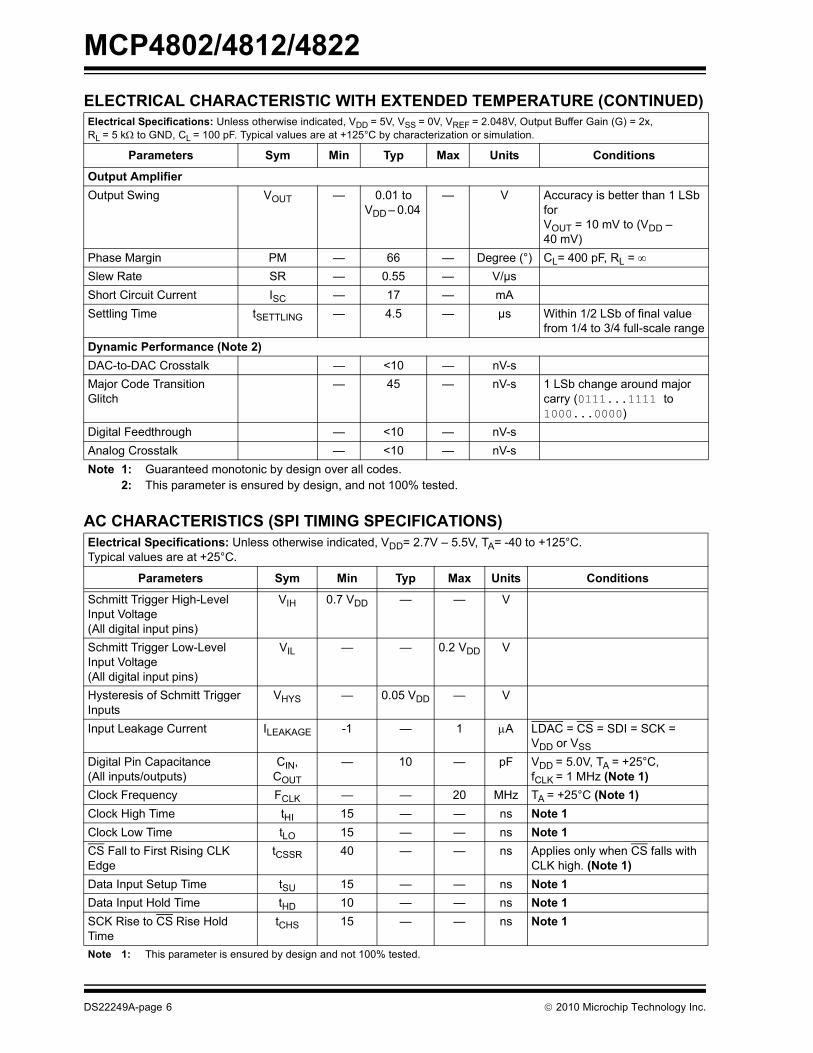
Output AmplifierOutput Swing VOUT — 0.01 to
VDD – 0.04 — V Accuracy is better than 1 LSb
for VOUT = 10 mV to (VDD – 40 mV)
Phase Margin PM — 66 — Degree (°) CL= 400 pF, RL = Slew Rate SR — 0.55 — V/µsShort Circuit Current ISC — 17 — mASettling Time tSETTLING — 4.5 — µs Within 1/2 LSb of final value
from 1/4 to 3/4 full-scale rangeDynamic Performance (Note 2)DAC-to-DAC Crosstalk — <10 — nV-sMajor Code Transition Glitch
— 45 — nV-s 1 LSb change around major carry (0111...1111 to 1000...0000)
Digital Feedthrough — <10 — nV-sAnalog Crosstalk — <10 — nV-s
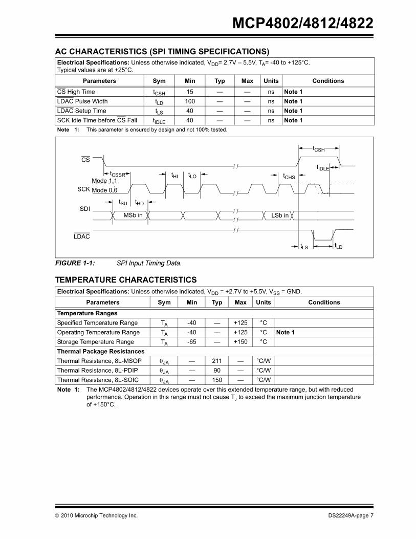
AC CHARACTERISTICS (SPI TIMING SPECIFICATIONS)Electrical Specifications: Unless otherwise indicated, VDD= 2.7V – 5.5V, TA= -40 to +125°C. Typical values are at +25°C.
Parameters Sym Min Typ Max Units Conditions
Schmitt Trigger High-Level Input Voltage(All digital input pins)
VIH 0.7 VDD — — V
Schmitt Trigger Low-Level Input Voltage (All digital input pins)
VIL — — 0.2 VDD V
Hysteresis of Schmitt Trigger Inputs
VHYS — 0.05 VDD — V
Input Leakage Current ILEAKAGE -1 — 1 A LDAC = CS = SDI = SCK = VDD or VSS
Digital Pin Capacitance(All inputs/outputs)
CIN, COUT
— 10 — pF VDD = 5.0V, TA = +25°C, fCLK = 1 MHz (Note 1)
Clock Frequency FCLK — — 20 MHz TA = +25°C (Note 1)Clock High Time tHI 15 — — ns Note 1Clock Low Time tLO 15 — — ns Note 1CS Fall to First Rising CLK Edge
tCSSR 40 — — ns Applies only when CS falls with CLK high. (Note 1)
Data Input Setup Time tSU 15 — — ns Note 1Data Input Hold Time tHD 10 — — ns Note 1SCK Rise to CS Rise Hold Time
tCHS 15 — — ns Note 1
Note 1: This parameter is ensured by design and not 100% tested.
ELECTRICAL CHARACTERISTIC WITH EXTENDED TEMPERATURE (CONTINUED)Electrical Specifications: Unless otherwise indicated, VDD = 5V, VSS = 0V, VREF = 2.048V, Output Buffer Gain (G) = 2x, RL = 5 k to GND, CL = 100 pF. Typical values are at +125°C by characterization or simulation.
Parameters Sym Min Typ Max Units Conditions
Note 1: Guaranteed monotonic by design over all codes.2: This parameter is ensured by design, and not 100% tested.
DS22249A-page 6 2010 Microchip Technology Inc.
MCP4802/4812/4822
FIGURE 1-1: SPI Input Timing Data.
TEMPERATURE CHARACTERISTICS
CS High Time tCSH 15 — — ns Note 1LDAC Pulse Width tLD 100 — — ns Note 1LDAC Setup Time tLS 40 — — ns Note 1SCK Idle Time before CS Fall tIDLE 40 — — ns Note 1
Electrical Specifications: Unless otherwise indicated, VDD = +2.7V to +5.5V, VSS = GND.
Parameters Sym Min Typ Max Units Conditions
Temperature RangesSpecified Temperature Range TA -40 — +125 °COperating Temperature Range TA -40 — +125 °C Note 1Storage Temperature Range TA -65 — +150 °CThermal Package ResistancesThermal Resistance, 8L-MSOP JA — 211 — °C/WThermal Resistance, 8L-PDIP JA — 90 — °C/WThermal Resistance, 8L-SOIC JA — 150 — °C/WNote 1: The MCP4802/4812/4822 devices operate over this extended temperature range, but with reduced
performance. Operation in this range must not cause TJ to exceed the maximum junction temperature of +150°C.
AC CHARACTERISTICS (SPI TIMING SPECIFICATIONS)Electrical Specifications: Unless otherwise indicated, VDD= 2.7V – 5.5V, TA= -40 to +125°C. Typical values are at +25°C.
Parameters Sym Min Typ Max Units Conditions
Note 1: This parameter is ensured by design and not 100% tested.
CS
SCK
SDI
LDAC
tCSSR
tHDtSU
tLO
tCSH
tCHS
LSb inMSb in
tIDLE
Mode 1,1Mode 0,0
tHI
tLDtLS
2010 Microchip Technology Inc. DS22249A-page 7

MCP4802/4812/4822
NOTES:DS22249A-page 8 2010 Microchip Technology Inc.
MCP4802/4812/4822
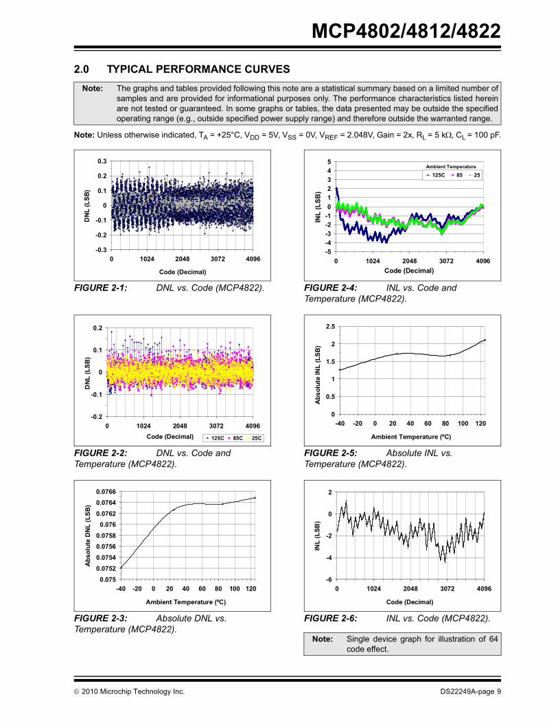
2.0 TYPICAL PERFORMANCE CURVES
Note: Unless otherwise indicated, TA = +25°C, VDD = 5V, VSS = 0V, VREF = 2.048V, Gain = 2x, RL = 5 k, CL = 100 pF.
FIGURE 2-1: DNL vs. Code (MCP4822).
FIGURE 2-2: DNL vs. Code and Temperature (MCP4822).
FIGURE 2-3: Absolute DNL vs. Temperature (MCP4822).
FIGURE 2-4: INL vs. Code and Temperature (MCP4822).
FIGURE 2-5: Absolute INL vs. Temperature (MCP4822).
FIGURE 2-6: INL vs. Code (MCP4822).
Note: The graphs and tables provided following this note are a statistical summary based on a limited number ofsamples and are provided for informational purposes only. The performance characteristics listed hereinare not tested or guaranteed. In some graphs or tables, the data presented may be outside the specifiedoperating range (e.g., outside specified power supply range) and therefore outside the warranted range.
-0.3
-0.2
-0.1
0
0.1
0.2
0.3
0 1024 2048 3072 4096
Code (Decimal)
DN
L (L
SB)
-0.2
-0.1
0
0.1
0.2
0 1024 2048 3072 4096Code (Decimal)
DNL
(LSB
)
125C 85C 25C
0.0750.07520.07540.07560.0758
0.0760.07620.07640.0766
-40 -20 0 20 40 60 80 100 120
Ambient Temperature (ºC)
Abs
olut
e D
NL
(LSB
)
Note: Single device graph for illustration of 64code effect.
-5-4-3-2-1012345
0 1024 2048 3072 4096Code (Decimal)
INL
(LSB
)
125C 85 25Ambient Temperature
0
0.5
1
1.5
2
2.5
-40 -20 0 20 40 60 80 100 120
Ambient Temperature (ºC)
Abs
olut
e IN
L (L
SB)
-6
-4
-2
0
2
0 1024 2048 3072 4096
Code (Decimal)
INL
(LSB
)
2010 Microchip Technology Inc. DS22249A-page 9
MCP4802/4812/4822
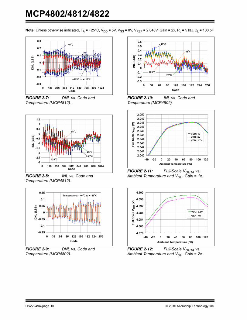
Note: Unless otherwise indicated, TA = +25°C, VDD = 5V, VSS = 0V, VREF = 2.048V, Gain = 2x, RL = 5 k, CL = 100 pF.FIGURE 2-7: DNL vs. Code and Temperature (MCP4812).
FIGURE 2-8: INL vs. Code and Temperature (MCP4812).
FIGURE 2-9: DNL vs. Code and Temperature (MCP4802).
FIGURE 2-10: INL vs. Code and Temperature (MCP4802).
FIGURE 2-11: Full-Scale VOUTA vs. Ambient Temperature and VDD. Gain = 1x.
FIGURE 2-12: Full-Scale VOUTA vs. Ambient Temperature and VDD. Gain = 2x.
-0.3
-0.2
-0.1
0
0.1
0.2
0.3
0 128 256 384 512 640 768 896 1024Code
DN
L (L
SB)
- 40oC
+25oC to +125oC
-3
-2.5
-2
-1.5
-1
-0.5
0
0.5
1
1.5
0 128 256 384 512 640 768 896 1024Code
INL
(LSB
)
25oC
85oC
125oC- 40oC
-0.15
-0.1
-0.05
0
0.05
0.1
0.15
0 32 64 96 128 160 192 224 256Code
DN
L (L
SB)
34
Temperature: - 40oC to +125oC
-0.3-0.2-0.1
00.10.20.30.40.50.6
0 32 64 96 128 160 192 224 256Code
INL
(LSB
)
- 40oC
25oC
85oC
125oC
2.0402.0412.0422.0432.0442.0452.0462.0472.0482.0492.050
-40 -20 0 20 40 60 80 100 120Ambient Temperature (°C)
Full
Scal
e V O
UT (
V)VDD: 4VVDD: 3VVDD: 2.7V
4.076
4.080
4.084
4.088
4.092
4.096
4.100
-40 -20 0 20 40 60 80 100 120Ambient Temperature (°C)
Full
Scal
e V O
UT (
V)
VDD: 5.5V
VDD: 5V
DS22249A-page 10 2010 Microchip Technology Inc.
MCP4802/4812/4822
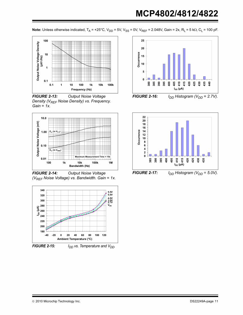
Note: Unless otherwise indicated, TA = +25°C, VDD = 5V, VSS = 0V, VREF = 2.048V, Gain = 2x, RL = 5 k, CL = 100 pF.FIGURE 2-13: Output Noise Voltage Density (VREF Noise Density) vs. Frequency. Gain = 1x.
FIGURE 2-14: Output Noise Voltage (VREF Noise Voltage) vs. Bandwidth. Gain = 1x.
FIGURE 2-15: IDD vs. Temperature and VDD.
FIGURE 2-16: IDD Histogram (VDD = 2.7V).
FIGURE 2-17: IDD Histogram (VDD = 5.0V).
1.E-07
1.E-06
1.E-05
1.E-04
1E-1 1E+0 1E+1 1E+2 1E+3 1E+4 1E+5Frequency (Hz)
Out
put N
oise
Vol
tage
Den
sity
(µV/H
z)
0.1 1 10 100 1k 10k 100k
100
10
1
0.1
1.E-05
1.E-04
1.E-03
1.E-02
1E+2 1E+3 1E+4 1E+5 1E+6Bandwidth (Hz)
Out
put N
oise
Vol
tage
(mV)
100 1k 10k 100k 1M
Eni (in VRMS)
10.0
1.00
0.10
0.01
Eni (in VP-P)
Maximum Measurement Time = 10s
180
200
220
240
260
280
300
320
340
-40 -20 0 20 40 60 80 100 120Ambient Temperature (°C)
I DD (µ
A) VDD
5.5V
4.0V5.0V
3.0V2.7V
0
5
10
15
20
25
380
385
390
395
400
405
410
415
420
425
430
435
440
IDD (µA)
Occ
urre
nce
02468
10121416182022
385
390
395
400
405
410
415
420
425
430
435
IDD (µA)
Occ
urre
nce
2010 Microchip Technology Inc. DS22249A-page 11
MCP4802/4812/4822
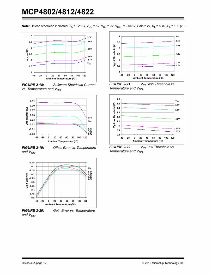
Note: Unless otherwise indicated, TA = +25°C, VDD = 5V, VSS = 0V, VREF = 2.048V, Gain = 2x, RL = 5 k, CL = 100 pF.FIGURE 2-18: Software Shutdown Current vs. Temperature and VDD.
FIGURE 2-19: Offset Error vs. Temperature and VDD.
FIGURE 2-20: Gain Error vs. Temperature and VDD.
FIGURE 2-21: VIN High Threshold vs. Temperature and VDD.
FIGURE 2-22: VIN Low Threshold vs. Temperature and VDD.
1
1.5
2
2.5
3
3.5
4
-40 -20 0 20 40 60 80 100 120Ambient Temperature (ºC)
I SH
DN
_SW
(µA
)
VDD
5.5V
4.0V
5.0V
3.0V2.7V
-0.03
-0.01
0.01
0.03
0.05
0.07
0.09
0.11
-40 -20 0 20 40 60 80 100 120Ambient Temperature (ºC)
Offs
et E
rror
(%)
VDD
5.5V
4.0V5.0V
3.0V2.7V
-0.5
-0.45
-0.4
-0.35
-0.3-0.25
-0.2
-0.15
-0.1
-0.05
-40 -20 0 20 40 60 80 100 120Ambient Temperature (ºC)
Gai
n Er
ror (
%)
VDD
5.5V4.0V5.0V
3.0V2.7V
1
1.5
2
2.5
3
3.5
4
-40 -20 0 20 40 60 80 100 120Ambient Temperature (ºC)
V IN H
i Thr
esho
ld (V
)
VDD
5.5V
4.0V
5.0V
3.0V2.7V
0.8
0.9
1
1.1
1.2
1.3
1.4
1.5
1.6
-40 -20 0 20 40 60 80 100 120Ambient Temperature (ºC)
V IN L
ow T
hres
hold
(V)
VDD
5.5V
4.0V
5.0V
3.0V2.7V
DS22249A-page 12 2010 Microchip Technology Inc.
MCP4802/4812/4822
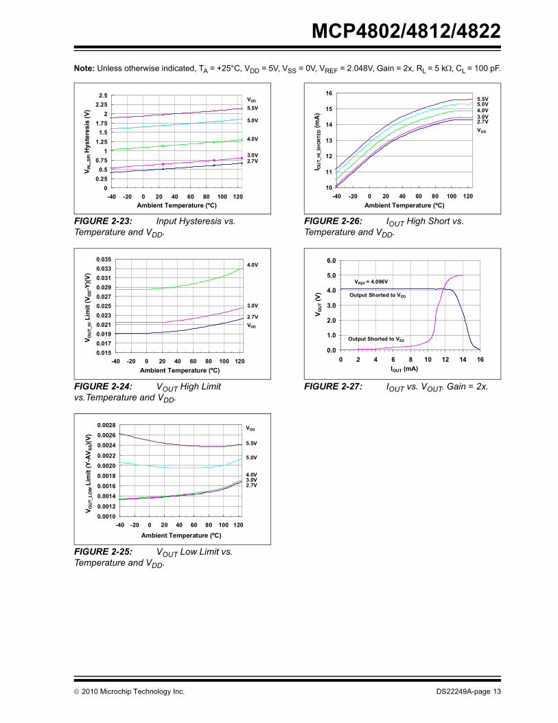
Note: Unless otherwise indicated, TA = +25°C, VDD = 5V, VSS = 0V, VREF = 2.048V, Gain = 2x, RL = 5 k, CL = 100 pF.FIGURE 2-23: Input Hysteresis vs. Temperature and VDD.
FIGURE 2-24: VOUT High Limit vs.Temperature and VDD.
FIGURE 2-25: VOUT Low Limit vs. Temperature and VDD.
FIGURE 2-26: IOUT High Short vs. Temperature and VDD.
FIGURE 2-27: IOUT vs. VOUT. Gain = 2x.
00.25
0.50.75
11.25
1.51.75
22.25
2.5
-40 -20 0 20 40 60 80 100 120Ambient Temperature (ºC)
V IN_ S
PI H
yste
resi
s (V
)
VDD
5.5V
4.0V
5.0V
3.0V2.7V
0.0150.0170.0190.0210.0230.0250.0270.0290.0310.0330.035
-40 -20 0 20 40 60 80 100 120Ambient Temperature (ºC)
V OU
T_H
I Lim
it (V
DD-Y
)(V)
VDD
4.0V
3.0V
2.7V
0.00100.0012
0.00140.00160.00180.00200.0022
0.00240.00260.0028
-40 -20 0 20 40 60 80 100 120
Ambient Temperature (ºC)
V OU
T_LO
W L
imit
(Y-A
V SS)
(V)
VDD
5.5V
4.0V
5.0V
3.0V2.7V
10
11
12
13
14
15
16
-40 -20 0 20 40 60 80 100 120Ambient Temperature (ºC)
I OU
T_H
I_SH
OR
TED (m
A)
VDD
5.5V
4.0V5.0V
3.0V2.7V
0.0
1.0
2.0
3.0
4.0
5.0
6.0
0 2 4 6 8 10 12 14 16IOUT (mA)
V OU
T (V)
VREF = 4.096V
Output Shorted to VSS
Output Shorted to VDD
2010 Microchip Technology Inc. DS22249A-page 13
MCP4802/4812/4822
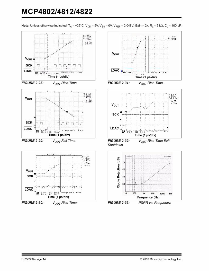
Note: Unless otherwise indicated, TA = +25°C, VDD = 5V, VSS = 0V, VREF = 2.048V, Gain = 2x, RL = 5 k, CL = 100 pF.FIGURE 2-28: VOUT Rise Time.
FIGURE 2-29: VOUT Fall Time.
FIGURE 2-30: VOUT Rise Time.
FIGURE 2-31: VOUT Rise Time.
FIGURE 2-32: VOUT Rise Time Exit Shutdown.
FIGURE 2-33: PSRR vs. Frequency.
VOUT
SCK
LDAC
Time (1 µs/div)
VOUT
SCK
LDAC
Time (1 µs/div)
VOUT
SCK
LDAC
Time (1 µs/div)
Time (1 µs/div)
VOUT
LDAC
Time (1 µs/div)
VOUT
SCK
LDAC
Rip
ple
Rej
ectio
n (d
B)
Frequency (Hz)
DS22249A-page 14 2010 Microchip Technology Inc.
MCP4802/4812/4822
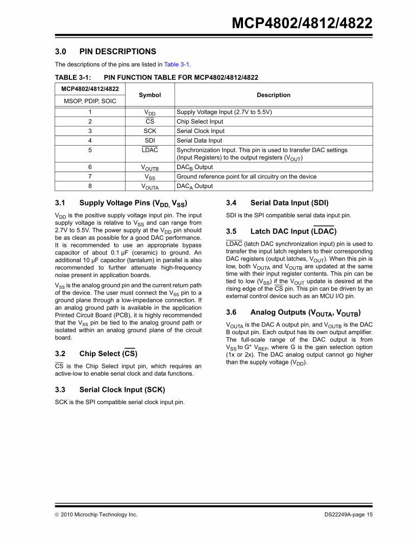
3.0 PIN DESCRIPTIONSThe descriptions of the pins are listed in Table 3-1.
3.1 Supply Voltage Pins (VDD, VSS)VDD is the positive supply voltage input pin. The inputsupply voltage is relative to VSS and can range from2.7V to 5.5V. The power supply at the VDD pin shouldbe as clean as possible for a good DAC performance.It is recommended to use an appropriate bypasscapacitor of about 0.1 µF (ceramic) to ground. Anadditional 10 µF capacitor (tantalum) in parallel is alsorecommended to further attenuate high-frequencynoise present in application boards.
VSS is the analog ground pin and the current return pathof the device. The user must connect the VSS pin to aground plane through a low-impedance connection. Ifan analog ground path is available in the applicationPrinted Circuit Board (PCB), it is highly recommendedthat the VSS pin be tied to the analog ground path orisolated within an analog ground plane of the circuitboard.
3.2 Chip Select (CS)CS is the Chip Select input pin, which requires anactive-low to enable serial clock and data functions.
3.3 Serial Clock Input (SCK)SCK is the SPI compatible serial clock input pin.
3.4 Serial Data Input (SDI)SDI is the SPI compatible serial data input pin.
3.5 Latch DAC Input (LDAC)LDAC (latch DAC synchronization input) pin is used totransfer the input latch registers to their correspondingDAC registers (output latches, VOUT). When this pin islow, both VOUTA and VOUTB are updated at the sametime with their input register contents. This pin can betied to low (VSS) if the VOUT update is desired at therising edge of the CS pin. This pin can be driven by anexternal control device such as an MCU I/O pin.
3.6 Analog Outputs (VOUTA, VOUTB)VOUTA is the DAC A output pin, and VOUTB is the DACB output pin. Each output has its own output amplifier.The full-scale range of the DAC output is fromVSS to G* VREF, where G is the gain selection option(1x or 2x). The DAC analog output cannot go higherthan the supply voltage (VDD).
TABLE 3-1: PIN FUNCTION TABLE FOR MCP4802/4812/4822MCP4802/4812/4822
Symbol DescriptionMSOP, PDIP, SOIC
1 VDD Supply Voltage Input (2.7V to 5.5V)2 CS Chip Select Input3 SCK Serial Clock Input4 SDI Serial Data Input5 LDAC Synchronization Input. This pin is used to transfer DAC settings
(Input Registers) to the output registers (VOUT)6 VOUTB DACB Output7 VSS Ground reference point for all circuitry on the device8 VOUTA DACA Output
2010 Microchip Technology Inc. DS22249A-page 15

MCP4802/4812/4822
NOTES:DS22249A-page 16 2010 Microchip Technology Inc.
MCP4802/4812/4822
4.0 GENERAL OVERVIEWThe MCP4802, MCP4812 and MCP4822 are dualvoltage output 8-bit, 10-bit and 12-bit DAC devices,respectively. These devices include rail-to-rail outputamplifiers, internal voltage reference, shutdown andreset-management circuitry. The devices use an SPIserial communication interface and operate with a sin-gle supply voltage from 2.7V to 5.5V.
The DAC input coding of these devices is straightbinary. Equation 4-1 shows the DAC analog outputvoltage calculation.
EQUATION 4-1: ANALOG OUTPUT VOLTAGE (VOUT)
The ideal output range of each device is:
• MCP4802 (n = 8)(a) 0.0V to 255/256 * 2.048V when gain setting = 1x.
(b) 0.0V to 255/256 * 4.096V when gain setting = 2x.
• MCP4812 (n = 10)(a) 0.0V to 1023/1024 * 2.048V when gain setting = 1x.
(b) 0.0V to 1023/1024 * 4.096V when gain setting = 2x.
• MCP4822 (n = 12)(a) 0.0V to 4095/4096 * 2.048V when gain setting = 1x.
(b) 0.0V to 4095/4096 * 4.096V when gain setting = 2x.
1 LSb is the ideal voltage difference between twosuccessive codes. Table 4-1 illustrates the LSbcalculation of each device.
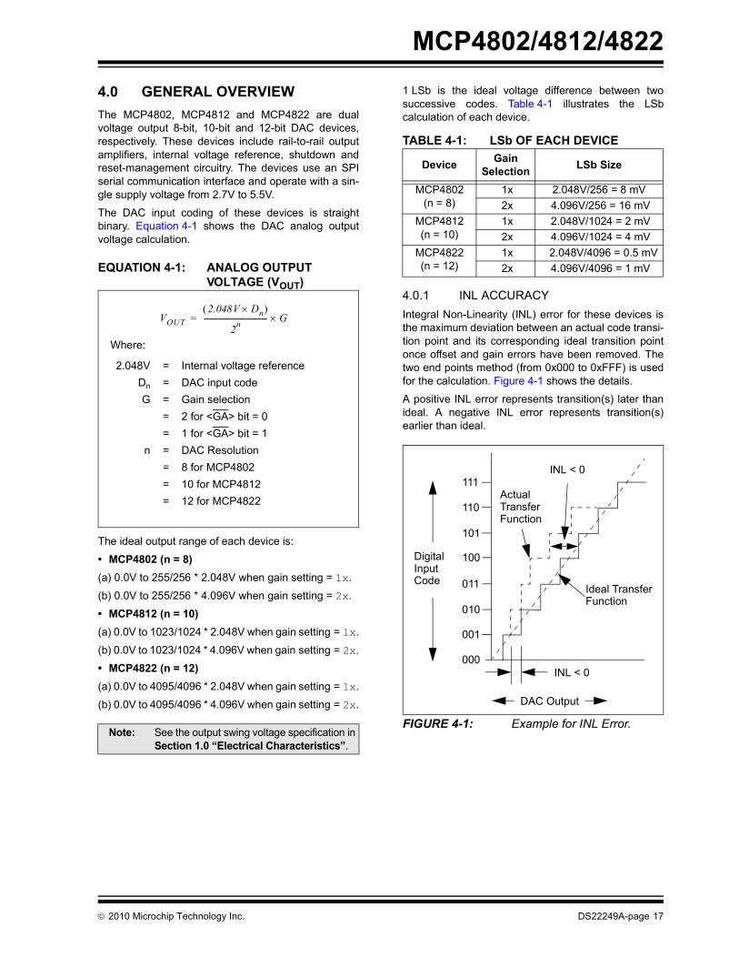
4.0.1 INL ACCURACYIntegral Non-Linearity (INL) error for these devices isthe maximum deviation between an actual code transi-tion point and its corresponding ideal transition pointonce offset and gain errors have been removed. Thetwo end points method (from 0x000 to 0xFFF) is usedfor the calculation. Figure 4-1 shows the details.
A positive INL error represents transition(s) later thanideal. A negative INL error represents transition(s)earlier than ideal.
FIGURE 4-1: Example for INL Error.Note: See the output swing voltage specification in
Section 1.0 “Electrical Characteristics”.
VOUT2.048V D n
2n----------------------------------- G=
Where:
2.048V = Internal voltage referenceDn = DAC input codeG = Gain selection
= 2 for <GA> bit = 0= 1 for <GA> bit = 1
n = DAC Resolution= 8 for MCP4802= 10 for MCP4812= 12 for MCP4822
TABLE 4-1: LSb OF EACH DEVICE
Device Gain Selection LSb Size
MCP4802 (n = 8)
1x 2.048V/256 = 8 mV 2x 4.096V/256 = 16 mV
MCP4812 (n = 10)
1x 2.048V/1024 = 2 mV 2x 4.096V/1024 = 4 mV
MCP4822 (n = 12)
1x 2.048V/4096 = 0.5 mV 2x 4.096V/4096 = 1 mV
111
110
101
100
011
010
001
000
DigitalInputCode
ActualTransferFunction
INL < 0
Ideal TransferFunction
INL < 0
DAC Output
2010 Microchip Technology Inc. DS22249A-page 17
MCP4802/4812/4822
4.0.2 DNL ACCURACYA Differential Non-Linearity (DNL) error is the measureof variations in code widths from the ideal code width.A DNL error of zero indicates that every code is exactly1 LSb wide.FIGURE 4-2: Example for DNL Error.
4.0.3 OFFSET ERRORAn offset error is the deviation from zero voltage outputwhen the digital input code is zero.
4.0.4 GAIN ERRORA gain error is the deviation from the ideal output,VREF – 1 LSb, excluding the effects of offset error.
4.1 Circuit Descriptions
4.1.1 OUTPUT AMPLIFIERSThe DAC’s outputs are buffered with a low-power,precision CMOS amplifier. This amplifier provides lowoffset voltage and low noise. The output stage enablesthe device to operate with output voltages close to thepower supply rails. Refer to Section 1.0 “ElectricalCharacteristics” for the analog output voltage rangeand load conditions.
In addition to resistive load-driving capability, theamplifier will also drive high capacitive loads withoutoscillation. The amplifier’s strong outputs allow VOUT tobe used as a programmable voltage reference in asystem.
4.1.1.1 Programmable Gain BlockThe rail-to-rail output amplifier has two configurablegain options: a gain of 1x (<GA> = 1) or a gain of 2x(<GA> = 0). The default value for this bit is a gainof 2 (<GA> = 0). This results in an ideal full-scaleoutput of 0.000V to 4.096V due to the internalreference (VREF = 2.048V).
4.1.2 VOLTAGE REFERENCE The MCP4802/4812/4822 devices utilize internal2.048V voltage reference. The voltage reference has alow temperature coefficient and low noisecharacteristics. Refer to Section 1.0 “Electrical Char-acteristics” for the voltage reference specifications.
111
110
101
100
011
010
001
000
DigitalInputCode
ActualTransferFunction
Ideal TransferFunction
Narrow Code, <1 LSb
DAC Output
Wide Code, >1 LSb
DS22249A-page 18 2010 Microchip Technology Inc.

MCP4802/4812/4822
4.1.3 POWER-ON RESET CIRCUITThe internal Power-on Reset (POR) circuit monitors thepower supply voltage (VDD) during the deviceoperation. The circuit also ensures that the DACpowers up with high output impedance (<SHDN> = 0,typically 500 k. The devices will continue to have ahigh-impedance output until a valid write command isreceived and the LDAC pin meets the input lowthreshold.If the power supply voltage is less than the PORthreshold (VPOR = 2.0V, typical), the DACs will be heldin their Reset state. The DACs will remain in that stateuntil VDD > VPOR and a subsequent write command isreceived.
Figure 4-3 shows a typical power supply transientpulse and the duration required to cause a reset tooccur, as well as the relationship between the durationand trip voltage. A 0.1 µF decoupling capacitor,mounted as close as possible to the VDD pin, canprovide additional transient immunity.
FIGURE 4-3: Typical Transient Response.
4.1.4 SHUTDOWN MODEThe user can shut down each DAC channel selectivelyusing a software command (<SHDN> = 0). DuringShutdown mode, most of the internal circuits in thechannel that was shut down are turned off for powersavings. The internal reference is not affected by theshutdown command. The serial interface also remainsactive, thus allowing a write command to bring thedevice out of the Shutdown mode. There will be noanalog output at the channel that was shut down andthe VOUT pin is internally switched to a known resistiveload (500 k typical. Figure 4-4 shows the analogoutput stage during the Shutdown mode.
The device will remain in Shutdown mode until the<SHDN> bit = 1 is latched into the device. When aDAC channel is changed from Shutdown to Activemode, the output settling time takes < 10 µs, butgreater than the standard active mode settling time(4.5 µs).
FIGURE 4-4: Output Stage for Shutdown Mode.
Transients above the curvewill cause a reset
Transients below the curvewill NOT cause a reset
5V
Time
Supp
ly V
olta
ges
Transient Duration
VPOR
VDD - VPOR
TA = +25°C
Tran
sien
t Dur
atio
n (µ
s)
10
8
6
4
2
01 2 3 4 5
VDD - VPOR (V)
500 k
Power-DownControl Circuit
ResistiveLoad
VOUTOpAmp
Resistive String DAC
2010 Microchip Technology Inc. DS22249A-page 19

MCP4802/4812/4822
NOTES:DS22249A-page 20 2010 Microchip Technology Inc.
MCP4802/4812/4822
5.0 SERIAL INTERFACE
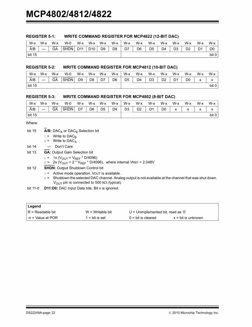
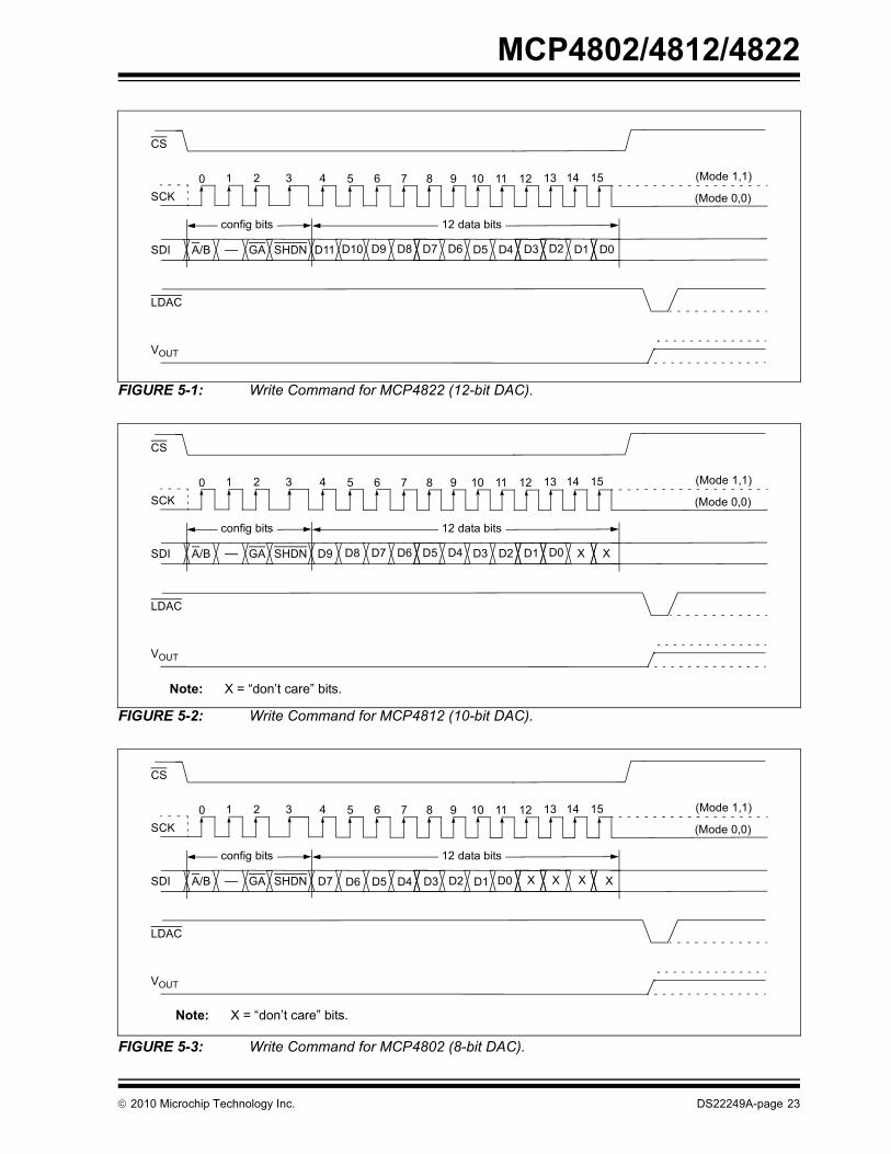
5.1 OverviewThe MCP4802/4812/4822 devices are designed tointerface directly with the Serial Peripheral Interface(SPI) port, available on many microcontrollers, andsupports Mode 0,0 and Mode 1,1. Commands and dataare sent to the device via the SDI pin, with data beingclocked-in on the rising edge of SCK. Thecommunications are unidirectional and, thus, datacannot be read out of the MCP4802/4812/4822devices. The CS pin must be held low for the durationof a write command. The write command consists of16 bits and is used to configure the DAC’s control anddata latches. Register 5-1 to Register 5-3 detail theinput register that is used to configure and load theDACA and DACB registers for each device. Figure 5-1to Figure 5-3 show the write command for each device.
Refer to Figure 1-1 and SPI Timing SpecificationsTable for detailed input and output timing specificationsfor both Mode 0,0 and Mode 1,1 operation.
5.2 Write CommandThe write command is initiated by driving the CS pinlow, followed by clocking the four Configuration bits andthe 12 data bits into the SDI pin on the rising edge ofSCK. The CS pin is then raised, causing the data to belatched into the selected DAC’s input registers.
The MCP4802/4812/4822 devices utilize a double-buffered latch structure to allow both DACA’s andDACB’s outputs to be synchronized with the LDAC pin,if desired.
By bringing down the LDAC pin to a low state, the con-tents stored in the DAC’s input registers are transferredinto the DAC’s output registers (VOUT), and both VOUTAand VOUTB are updated at the same time.
All writes to the MCP4802/4812/4822 devices are16-bit words. Any clocks after the first 16th clock will beignored. The Most Significant four bits areConfiguration bits. The remaining 12 bits are data bits.No data can be transferred into the device with CShigh. The data transfer will only occur if 16 clocks havebeen transferred into the device. If the rising edge ofCS occurs prior, shifting of data into the input registerswill be aborted.
2010 Microchip Technology Inc. DS22249A-page 21
MCP4802/4812/4822
REGISTER 5-1: WRITE COMMAND REGISTER FOR MCP4822 (12-BIT DAC)
REGISTER 5-2: WRITE COMMAND REGISTER FOR MCP4812 (10-BIT DAC)
REGISTER 5-3: WRITE COMMAND REGISTER FOR MCP4802 (8-BIT DAC)
Where:
W-x W-x W-x W-0 W-x W-x W-x W-x W-x W-x W-x W-x W-x W-x W-x W-xA/B — GA SHDN D11 D10 D9 D8 D7 D6 D5 D4 D3 D2 D1 D0
bit 15 bit 0
W-x W-x W-x W-0 W-x W-x W-x W-x W-x W-x W-x W-x W-x W-x W-x W-xA/B — GA SHDN D9 D8 D7 D6 D5 D4 D3 D2 D1 D0 x x
bit 15 bit 0
W-x W-x W-x W-0 W-x W-x W-x W-x W-x W-x W-x W-x W-x W-x W-x W-xA/B — GA SHDN D7 D6 D5 D4 D3 D2 D1 D0 x x x x
bit 15 bit 0
bit 15 A/B: DACA or DACB Selection bit1 = Write to DACB0 = Write to DACA
bit 14 — Don’t Care bit 13 GA: Output Gain Selection bit
1 = 1x (VOUT = VREF * D/4096)0 = 2x (VOUT = 2 * VREF * D/4096), where internal VREF = 2.048V.
bit 12 SHDN: Output Shutdown Control bit1 = Active mode operation. VOUT is available. 0 = Shutdown the selected DAC channel. Analog output is not available at the channel that was shut down. VOUT pin is connected to 500 ktypical)
bit 11-0 D11:D0: DAC Input Data bits. Bit x is ignored.
LegendR = Readable bit W = Writable bit U = Unimplemented bit, read as ‘0’-n = Value at POR 1 = bit is set 0 = bit is cleared x = bit is unknown
DS22249A-page 22 2010 Microchip Technology Inc.
MCP4802/4812/4822
FIGURE 5-1: Write Command for MCP4822 (12-bit DAC).
FIGURE 5-2: Write Command for MCP4812 (10-bit DAC).
FIGURE 5-3: Write Command for MCP4802 (8-bit DAC).
SDI
SCK
CS
0 21
A/B — GA SHDN D11 D10
config bits 12 data bits
LDAC
3 4
D9
5 6 7
D8 D7 D6
8 9 10 12
D5 D4 D3 D2 D1 D0
11 13 14 15
VOUT
(Mode 1,1)
(Mode 0,0)
SDI
SCK
CS
0 21
A/B — GA SHDN D9 D8
config bits 12 data bits
LDAC
3 4
D7
5 6 7
D6 D5 D4
8 9 10 12
D3 D2 D1 D0 X X
11 13 14 15
VOUT
(Mode 1,1)
(Mode 0,0)
Note: X = “don’t care” bits.
SDI
SCK
CS
0 21
A/B — GA SHDN
config bits 12 data bits
LDAC
3 4 5 6 7
XD7 D6
8 9 10 12
D5 D4 D3 D2 D1 D0
11 13 14 15
VOUT
(Mode 1,1)
(Mode 0,0)
X X X
Note: X = “don’t care” bits.
2010 Microchip Technology Inc. DS22249A-page 23

MCP4802/4812/4822
NOTES:DS22249A-page 24 2010 Microchip Technology Inc.
MCP4802/4812/4822
6.0 TYPICAL APPLICATIONSThe MCP4802/4812/4822 family of devices aregeneral purpose DACs for various applications wherea precision operation with low-power and internalvoltage reference is required.
Applications generally suited for the devices are:
• Set Point or Offset Trimming• Sensor Calibration• Precision Selectable Voltage Reference• Portable Instrumentation (Battery-Powered)• Calibration of Optical Communication Devices
6.1 Digital InterfaceThe MCP4802/4812/4822 devices utilize a 3-wiresynchronous serial protocol to transfer the DAC’s setupand input codes from the digital devices. The serialprotocol can be interfaced to SPI or Microwireperipherals that is common on many microcontrollerunits (MCUs), including Microchip’s PIC® MCUs anddsPIC® DSCs.
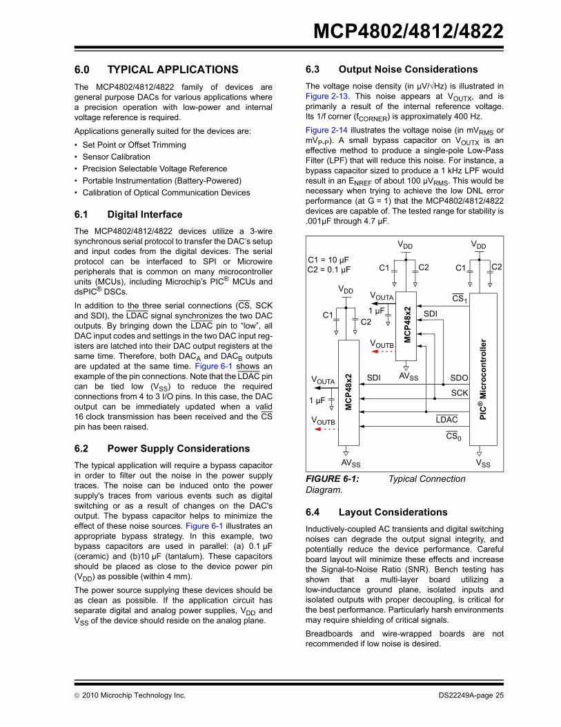
In addition to the three serial connections (CS, SCKand SDI), the LDAC signal synchronizes the two DACoutputs. By bringing down the LDAC pin to “low”, allDAC input codes and settings in the two DAC input reg-isters are latched into their DAC output registers at thesame time. Therefore, both DACA and DACB outputsare updated at the same time. Figure 6-1 shows anexample of the pin connections. Note that the LDAC pincan be tied low (VSS) to reduce the requiredconnections from 4 to 3 I/O pins. In this case, the DACoutput can be immediately updated when a valid16 clock transmission has been received and the CSpin has been raised.
6.2 Power Supply ConsiderationsThe typical application will require a bypass capacitorin order to filter out the noise in the power supplytraces. The noise can be induced onto the powersupply's traces from various events such as digitalswitching or as a result of changes on the DAC'soutput. The bypass capacitor helps to minimize theeffect of these noise sources. Figure 6-1 illustrates anappropriate bypass strategy. In this example, twobypass capacitors are used in parallel: (a) 0.1 µF(ceramic) and (b)10 µF (tantalum). These capacitorsshould be placed as close to the device power pin(VDD) as possible (within 4 mm).
The power source supplying these devices should beas clean as possible. If the application circuit hasseparate digital and analog power supplies, VDD andVSS of the device should reside on the analog plane.
6.3 Output Noise ConsiderationsThe voltage noise density (in µV/Hz) is illustrated inFigure 2-13. This noise appears at VOUTX, and isprimarily a result of the internal reference voltage.Its 1/f corner (fCORNER) is approximately 400 Hz.
Figure 2-14 illustrates the voltage noise (in mVRMS ormVP-P). A small bypass capacitor on VOUTX is aneffective method to produce a single-pole Low-PassFilter (LPF) that will reduce this noise. For instance, abypass capacitor sized to produce a 1 kHz LPF wouldresult in an ENREF of about 100 µVRMS. This would benecessary when trying to achieve the low DNL errorperformance (at G = 1) that the MCP4802/4812/4822devices are capable of. The tested range for stability is.001µF through 4.7 µF.
FIGURE 6-1: Typical Connection Diagram.
6.4 Layout ConsiderationsInductively-coupled AC transients and digital switchingnoises can degrade the output signal integrity, andpotentially reduce the device performance. Carefulboard layout will minimize these effects and increasethe Signal-to-Noise Ratio (SNR). Bench testing hasshown that a multi-layer board utilizing alow-inductance ground plane, isolated inputs andisolated outputs with proper decoupling, is critical forthe best performance. Particularly harsh environmentsmay require shielding of critical signals.
Breadboards and wire-wrapped boards are notrecommended if low noise is desired.
VDD
VDD VDD
AVSS
AVSS VSS
VOUTA
VOUTB
PIC
® M
icro
cont
rolle
r
VOUTA
VOUTB
SDI
SDI
CS1
SDO
SCK
LDAC
CS0
1 µF
1 µF
MC
P48x
2
MC
P48x
2
C1 = 10 µFC2 = 0.1 µF C1 C2 C2C1
C1C2
2010 Microchip Technology Inc. DS22249A-page 25

MCP4802/4812/4822
6.5 Single-Supply OperationThe MCP4802/4812/4822 family of devices are rail-to-rail voltage output DAC devices designed to operatewith a VDD range of 2.7V to 5.5V. Its output amplifier isrobust enough to drive small-signal loads directly.Therefore, it does not require any external output bufferfor most applications.6.5.1 DC SET POINT OR CALIBRATIONA common application for the devices is a digitally-controlled set point and/or calibration of variableparameters, such as sensor offset or slope. Forexample, the MCP4822 provides 4096 output steps. IfG = 1 is selected, the internal 2.048V VREF wouldproduce 500 µV of resolution. If G = 2 is selected, theinternal 2.048 VREF would produce 1 mV of resolution.
6.5.1.1 Decreasing Output Step Size If the application is calibrating the bias voltage of adiode or transistor, a bias voltage range of 0.8V may bedesired with about 200 µV resolution per step. Twocommon methods to achieve a 0.8V range are to eitherreduce VREF to 0.82V (using the MCP49XX familydevice that uses external reference) or use a voltagedivider on the DAC’s output.
Using a VREF is an option if the VREF is available withthe desired output voltage range. However,occasionally, when using a low-voltage VREF, the noisefloor causes SNR error that is intolerable. Using avoltage divider method is another option and providessome advantages when VREF needs to be very low orwhen the desired output voltage is not available. In thiscase, a larger value VREF is used while two resistorsscale the output range down to the precise desiredlevel.
Example 6-1 illustrates this concept. Note that thebypass capacitor on the output of the voltage dividerplays a critical function in attenuating the output noiseof the DAC and the induced noise from the environ-ment.
EXAMPLE 6-1: EXAMPLE CIRCUIT OF SET POINT OR THRESHOLD CALIBRATION
VDD
SPI3-wire
VTRIPR1
R2 0.1 µF
Comparator
VOUT 2.048 GDn2N------ =
VCC+
VCC–
VOUT
Vtrip VOUTR2
R1 R2+--------------------
=
VDD
RSENSE
DAC
(a) Single Output DAC:MCP4801MCP4811MCP4821
(b) Dual Output DAC:MCP4802MCP4812MCP4822
G = Gain selection (1x or 2x)Dn = Digital value of DAC (0-255) for MCP4801/MCP4802
= Digital value of DAC (0-1023) for MCP4811/MCP4812= Digital value of DAC (0-4095) for MCP4821/MCP4822
N = DAC bit resolution
DS22249A-page 26 2010 Microchip Technology Inc.
MCP4802/4812/4822
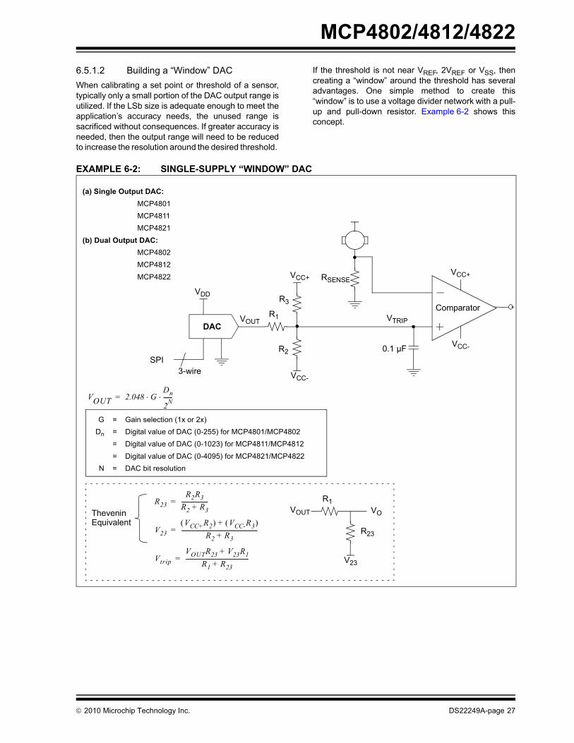
6.5.1.2 Building a “Window” DACWhen calibrating a set point or threshold of a sensor,typically only a small portion of the DAC output range isutilized. If the LSb size is adequate enough to meet theapplication’s accuracy needs, the unused range issacrificed without consequences. If greater accuracy isneeded, then the output range will need to be reducedto increase the resolution around the desired threshold.If the threshold is not near VREF, 2VREF or VSS, thencreating a “window” around the threshold has severaladvantages. One simple method to create this“window” is to use a voltage divider network with a pull-up and pull-down resistor. Example 6-2 shows thisconcept.
EXAMPLE 6-2: SINGLE-SUPPLY “WINDOW” DAC
DAC
VDD
SPI3-wire
VTRIPR1
R2 0.1 µF
ComparatorR3
VCC-
VCC+VCC+
VCC-
VOUT
R23R2R3R2 R3+-------------------=
V23VCC+R2 VCC-R3 +
R2 R3+------------------------------------------------------=
VtripVOUTR23 V23R1+
R1 R23+---------------------------------------------=
R1
R23
V23
VOUT VOTheveninEquivalent
RSENSE
VOUT 2.048 GDn2N------ =
(a) Single Output DAC:MCP4801MCP4811MCP4821
(b) Dual Output DAC:MCP4802MCP4812MCP4822
G = Gain selection (1x or 2x)Dn = Digital value of DAC (0-255) for MCP4801/MCP4802
= Digital value of DAC (0-1023) for MCP4811/MCP4812= Digital value of DAC (0-4095) for MCP4821/MCP4822
N = DAC bit resolution
2010 Microchip Technology Inc. DS22249A-page 27

MCP4802/4812/4822
6.6 Bipolar OperationBipolar operation is achievable using theMCP4802/4812/4822 family of devices by utilizing anexternal operational amplifier (op amp). Thisconfiguration is desirable due to the wide variety andavailability of op amps. This allows a general purposeDAC, with its cost and availability advantages, to meetalmost any desired output voltage range, power andnoise performance.Example 6-3 illustrates a simple bipolar voltage sourceconfiguration. R1 and R2 allow the gain to be selected,while R3 and R4 shift the DAC's output to a selectedoffset. Note that R4 can be tied to VDD, instead of VSS,if a higher offset is desired. Also note that a pull-up toVDD could be used instead of R4, or in addition to R4, ifa higher offset is desired.
EXAMPLE 6-3: DIGITALLY-CONTROLLED BIPOLAR VOLTAGE SOURCE
6.6.1 DESIGN EXAMPLE: DESIGN A BIPOLAR DAC USING EXAMPLE 6-3 WITH 12-BIT MCP4822 OR MCP4821
An output step magnitude of 1 mV, with an output rangeof ±2.05V, is desired for a particular application.
Step 1: Calculate the range: +2.05V – (-2.05V) = 4.1V.
Step 2: Calculate the resolution needed:
4.1V/1 mV = 4100
Since 212 = 4096, 12-bit resolution isdesired.
Step 3:The amplifier gain (R2/R1), multiplied by full-scale VOUT (4.096V), must be equal to thedesired minimum output to achieve bipolaroperation. Since any gain can be realized bychoosing resistor values (R1+R2), the VREFvalue must be selected first. If a VREF of 4.096Vis used (G=2), solve for the amplifier’s gain bysetting the DAC to 0, knowing that the outputneeds to be -2.05V.
The equation can be simplified to:
Step 4: Next, solve for R3 and R4 by setting the DAC to4096, knowing that the output needs to be+2.05V.
DAC
VDD
VDD
SPI3-wire
VOUTR3
R4
R2
R1
VIN+
0.1 µF
VCC+
VCC–
VIN+VOUTR4R3 R4+--------------------=
VO
VO VIN+ 1R2R1------+
VDDR2R1------ –=
VOUT 2.048 GDn2N------ =
(a) Single Output DAC:MCP4801MCP4811MCP4821
(b) Dual Output DAC:MCP4802MCP4812MCP4822
G = Gain selection (1x or 2x)Dn = Digital value of DAC (0-255) for MCP4801/MCP4802
= Digital value of DAC (0-1023) for MCP4811/MCP4812= Digital value of DAC (0-4095) for MCP4821/MCP4822
N = DAC bit resolution
R2–
R1--------- 2.05–
4.096V-----------------=
If R1 = 20 k and R2 = 10 k, the gain will be 0.5.
R2R1------ 1
2---=
R4R3 R4+ ------------------------ 2.05V 0.5 4.096V +
1.5 4.096V------------------------------------------------------- 2
3---= =
If R4 = 20 k, then R3 = 10 k
DS22249A-page 28 2010 Microchip Technology Inc.

MCP4802/4812/4822
6.7 Selectable Gain andOffset Bipolar Voltage Output Using a Dual Output DAC
In some applications, precision digital control of theoutput range is desirable. Example 6-4 illustrates howto use the MCP4802/4812/4822 family of devices toachieve this in a bipolar or single-supply application.
This circuit is typically used for linearizing a sensorwhose slope and offset varies.
The equation to design a bipolar “window” DAC wouldbe utilized if R3, R4 and R5 are populated.
EXAMPLE 6-4: BIPOLAR VOLTAGE SOURCE WITH SELECTABLE GAIN AND OFFSET
VDD
R3
R4
R2
VO
DACA
VDD
R1
(DACA for Gain Adjust)
(DACB for Offset Adjust)SPI
3
R5
VCC+
Thevenin
Bipolar “Window” DAC using R4 and R5
0.1 µF
VCC–
VCC+
VCC–
VOUTA
VOUTB
VIN+VOUTBR4 VCC-R3+
R3 R4+-------------------------------------------------=
VO VIN+ 1R2R1------+
VOUTAR2R1------ –=
Equivalent V45VCC+R4 VCC-R5+
R4 R5+---------------------------------------------= R45R4R5R4 R5+-------------------=
VIN+VOUTBR45 V45R3+
R3 R45+------------------------------------------------= VO VIN+ 1R2R1------+
VOUTAR2R1------ –=
Offset Adjust Gain Adjust
Offset Adjust Gain Adjust
DACB
VOUTA 2.048 GADn2N------ =
VOUTB 2.048 GBDn2N------ =
VIN+
Dual Output DAC:MCP4802MCP4812MCP4822
G = Gain selection (1x or 2x)N = DAC bit resolution
DA , DB = Digital value of DAC (0-255) for MCP4802= Digital value of DAC (0-1023) for MCP4812= Digital value of DAC (0-4095) for MCP4822
2010 Microchip Technology Inc. DS22249A-page 29
MCP4802/4812/4822
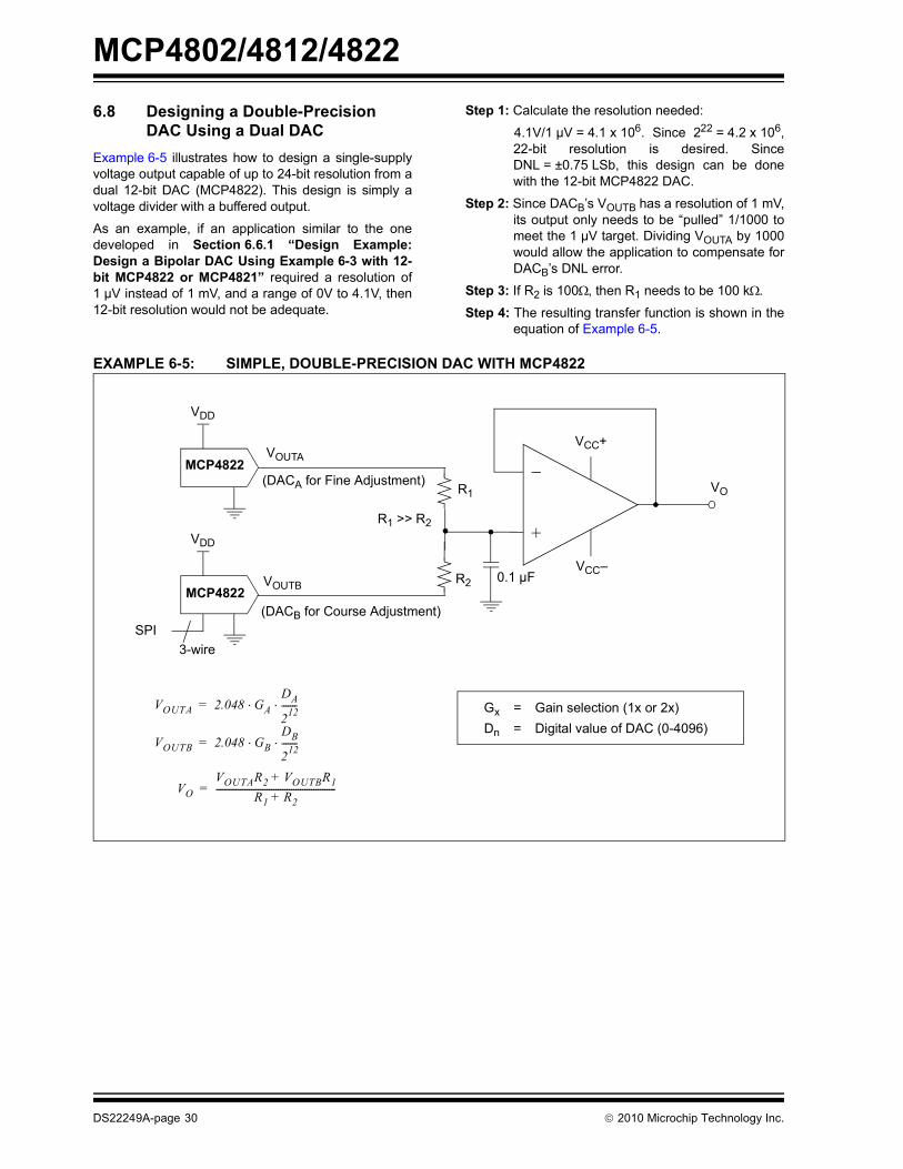
6.8 Designing a Double-PrecisionDAC Using a Dual DACExample 6-5 illustrates how to design a single-supplyvoltage output capable of up to 24-bit resolution from adual 12-bit DAC (MCP4822). This design is simply avoltage divider with a buffered output.
As an example, if an application similar to the onedeveloped in Section 6.6.1 “Design Example:Design a Bipolar DAC Using Example 6-3 with 12-bit MCP4822 or MCP4821” required a resolution of1 µV instead of 1 mV, and a range of 0V to 4.1V, then12-bit resolution would not be adequate.
Step 1: Calculate the resolution needed:
4.1V/1 µV = 4.1 x 10⁶. Since 222 = 4.2 x 106,22-bit resolution is desired. SinceDNL = ±0.75 LSb, this design can be donewith the 12-bit MCP4822 DAC.
Step 2: Since DACB’s VOUTB has a resolution of 1 mV,its output only needs to be “pulled” 1/1000 tomeet the 1 µV target. Dividing VOUTA by 1000would allow the application to compensate forDACB’s DNL error.
Step 3: If R2 is 100, then R1 needs to be 100 k.
Step 4: The resulting transfer function is shown in theequation of Example 6-5.
EXAMPLE 6-5: SIMPLE, DOUBLE-PRECISION DAC WITH MCP4822
VDD
R2
VO
VDD
R1(DACA for Fine Adjustment)
(DACB for Course Adjustment)SPI
3-wire
R1 >> R2
VOVOUTAR2 VOUTBR1+
R1 R2+------------------------------------------------------=
0.1 µF
VCC+
VCC–
VOUTA
VOUTB
VOUTA 2.048 GADA212------- =
VOUTB 2.048 GBDB212------- =
MCP4822
MCP4822
Gx = Gain selection (1x or 2x)Dn = Digital value of DAC (0-4096)
DS22249A-page 30 2010 Microchip Technology Inc.
MCP4802/4812/4822
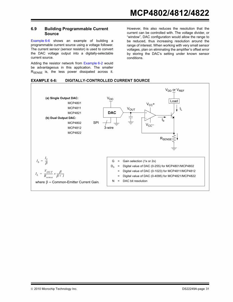
6.9 Building Programmable CurrentSourceExample 6-6 shows an example of building aprogrammable current source using a voltage follower.The current sensor (sensor resistor) is used to convertthe DAC voltage output into a digitally-selectablecurrent source.
Adding the resistor network from Example 6-2 wouldbe advantageous in this application. The smallerRSENSE is, the less power dissipated across it.
However, this also reduces the resolution that thecurrent can be controlled with. The voltage divider, or“window”, DAC configuration would allow the range tobe reduced, thus increasing resolution around therange of interest. When working with very small sensorvoltages, plan on eliminating the amplifier’s offset errorby storing the DAC’s setting under known sensorconditions.
EXAMPLE 6-6: DIGITALLY-CONTROLLED CURRENT SOURCE
DAC
RSENSE
Ib
Load
IL
VDD
SPI3-wire
VCC+
VCC–
VOUT
ILVOUTRsense---------------
1+-------------=
IbIL----=
Common-Emitter Current Gainwhere
VDD or VREF
(a) Single Output DAC:MCP4801MCP4811MCP4821
(b) Dual Output DAC:MCP4802MCP4812MCP4822
G = Gain selection (1x or 2x)Dn = Digital value of DAC (0-255) for MCP4801/MCP4802
= Digital value of DAC (0-1023) for MCP4811/MCP4812= Digital value of DAC (0-4095) for MCP4821/MCP4822
N = DAC bit resolution
2010 Microchip Technology Inc. DS22249A-page 31

MCP4802/4812/4822
NOTES:DS22249A-page 32 2010 Microchip Technology Inc.
MCP4802/4812/4822
7.0 DEVELOPMENT SUPPORT
7.1 Evaluation and Demonstration Boards
The Mixed Signal PICtail™ Demo Board supports theMCP4802/4812/4822 family of devices. Refer towww.microchip.com for further information on thisproduct’s capabilities and availability.
2010 Microchip Technology Inc. DS22249A-page 33

MCP4802/4812/4822
NOTES:DS22249A-page 34 2010 Microchip Technology Inc.
MCP4802/4812/4822
8.0 PACKAGING INFORMATION
8.1 Package Marking Information
XXXXXXXXXXXXXNNN
YYWW
8-Lead PDIP (300 mil) Example:
8-Lead SOIC (150 mil) Example:
XXXXXXXXXXXXYYWW
NNN
MCP4802E/P ^ 256
1009
MCP4812ESN^^ 1009
256
8-Lead MSOP Example:
XXXXXXYWWNNN
4822E009256
Legend: XX...X Customer-specific informationY Year code (last digit of calendar year)YY Year code (last 2 digits of calendar year)WW Week code (week of January 1 is week ‘01’)NNN Alphanumeric traceability code Pb-free JEDEC designator for Matte Tin (Sn)* This package is Pb-free. The Pb-free JEDEC designator ( )
can be found on the outer packaging for this package.
Note: In the event the full Microchip part number cannot be marked on one line, it willbe carried over to the next line, thus limiting the number of availablecharacters for customer-specific information.
3e
3e
3e
3e
2010 Microchip Technology Inc. DS22249A-page 35
MCP4802/4812/4822
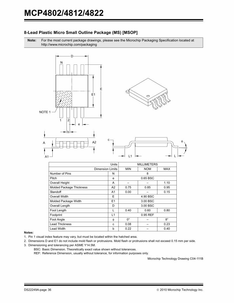
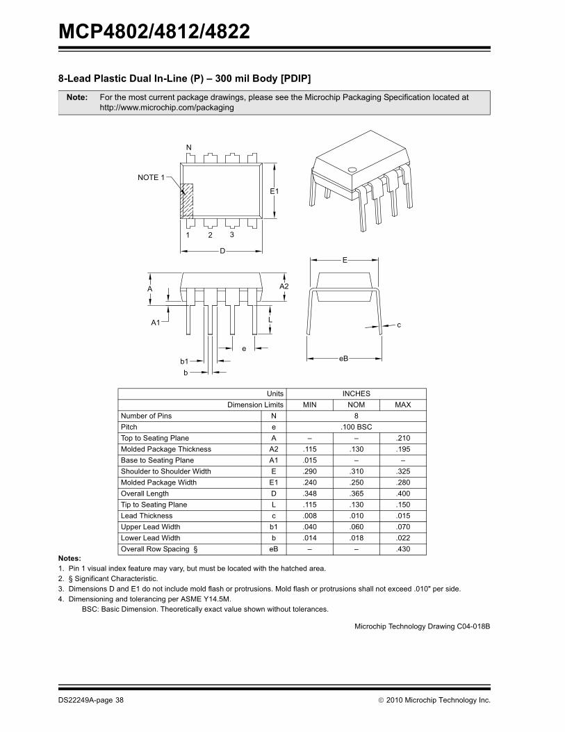
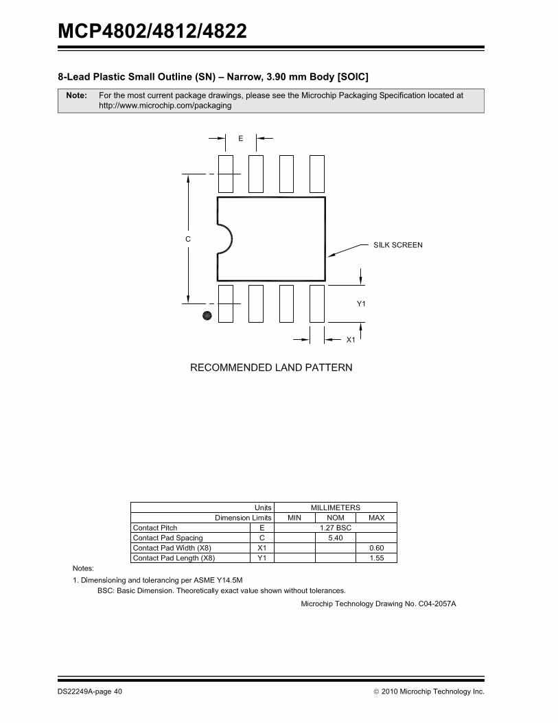
���������� ��� ����������� ��������������������
�������� �������� !�����"�#�$��%!��&������'�(!%�&! %�(�����%�"�)�%����%�����%���"������� ��&�� �� �����"�*��"��%�����!"��&�"�$�� ����%! �� ����"�$�� ����%! �� � ������%��#���"����+�&&���� �"��,� ��&�� ��������"�%���������������*�-���+��
.�/0 .� �����&�� ���� ���%��������#��%����!�� �)��)�%�!%�%������ ��*10 ��$��������&�� ��'�! !�����)�%�!%�%������'�$���$&�%����!� � �����
����� 1�%���& %��!��%����2����"�)��� '����� �� ���%��������������2�����������$���%������%�"��%��%%�033)))�&��������&3���2�����
4��% ��55��* *����&�� ���5�&�% ��6 67� ��8
6!&(��$���� 6 9��%�� � ��:+�.�/7������;����% � < < ������"�"����2���� ���2�� �� ���+ ��9+ ���+�%��"$$� �� ���� < ���+7������=�"%� * �����.�/��"�"����2����=�"%� *� ,����.�/7������5���%� � ,����.�/1%�5���%� 5 ���� ��:� ��9�1%���% 5� ���+��*11%������ � �> < 9>5��"� ���2�� � ���9 < ���,5��"�=�"%� ( ���� < ����
D
N
E
E1
NOTE 1
1 2e
b
A
A1
A2c
L1 L
φ
������� ������� ��)��� /������.
DS22249A-page 36 2010 Microchip Technology Inc.
MCP4802/4812/4822
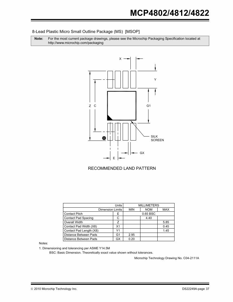
Note: For the most current package drawings, please see the Microchip Packaging Specification located at http://www.microchip.com/packaging
2010 Microchip Technology Inc. DS22249A-page 37
MCP4802/4812/4822
���������� ������ ��� ������!�"##�� �$��%��� �
�������� �������� !�����"�#�$��%!��&������'�(!%�&! %�(�����%�"�)�%��%�����%���"������� ?������$����%�/����%�� %���,� ��&�� �� �����"�*��"��%�����!"��&�"�$�� ����%! �� ����"�$�� ����%! �� � ������%��#���"�����@���� �"���� ��&�� ��������"�%���������������*�-���+��
.�/0�.� �����&�� ���� ���%��������#��%����!�� �)��)�%�!%�%������ �
����� 1�%���& %��!��%����2����"�)��� '����� �� ���%��������������2�����������$���%������%�"��%��%%�033)))�&��������&3���2�����
4��% �6/;*���&�� ���5�&�% ��6 67� ��8
6!&(��$���� 6 9��%�� � �����.�/ ��%����%��������� � < < ������"�"����2���� ���2�� �� ���+ ��,� ���+.� ��%����%��������� �� ���+ < <��!�"��%���!�"��=�"%� * ���� �,�� �,�+��"�"����2����=�"%� *� ���� ��+� ��9�7������5���%� � �,�9 �,:+ ���� ���%����%��������� 5 ���+ ��,� ��+�5��"� ���2�� � ���9 ���� ���+4����5��"�=�"%� (� ���� ��:� ����5)��5��"�=�"%� ( ���� ���9 ����7�������)����������? �. < < ��,�
N
E1
NOTE 1
D
1 2 3
A
A1
A2
L
b1b
e
E
eB
c
������� ������� ��)��� /�����9.
DS22249A-page 38 2010 Microchip Technology Inc.

MCP4802/4812/4822
���������� ��������� ��������!������&'�"()#����$��%���� *�
�������� �������� !�����"�#�$��%!��&������'�(!%�&! %�(�����%�"�)�%����%�����%���"������� ?������$����%�/����%�� %���,� ��&�� �� �����"�*��"��%�����!"��&�"�$�� ����%! �� ����"�$�� ����%! �� � ������%��#���"����+�&&���� �"���� ��&�� ��������"�%���������������*�-���+��
.�/0 .� �����&�� ���� ���%��������#��%����!�� �)��)�%�!%�%������ ��*10 ��$��������&�� ��'�! !�����)�%�!%�%������'�$���$&�%����!� � �����
����� 1�%���& %��!��%����2����"�)��� '����� �� ���%��������������2�����������$���%������%�"��%��%%�033)))�&��������&3���2�����
4��% ��55��* *����&�� ���5�&�% ��6 67� ��8
6!&(��$���� 6 9��%�� � �����.�/7������;����% � < < ���+��"�"����2���� ���2�� �� ���+ < <�%��"$$��? �� ���� < ���+7������=�"%� * :����.�/��"�"����2����=�"%� *� ,����.�/7������5���%� � �����.�//��&$��A�%����B � ���+ < ��+�1%�5���%� 5 ���� < ����1%���% 5� ������*11%������ � �> < 9>5��"� ���2�� � ���� < ���+5��"�=�"%� ( ��,� < ��+���"���$%������� � � +> < �+>��"���$%�������.%%& � +> < �+>
D
Ne
E
E1
NOTE 1
1 2 3
b
A
A1
A2
L
L1
c
h
h
φ
β
α
������� ������� ��)��� /����+�.
2010 Microchip Technology Inc. DS22249A-page 39
MCP4802/4812/4822
���������� ��������� ��������!������&'�"()#����$��%���� *�
����� 1�%���& %��!��%����2����"�)��� '����� �� ���%��������������2�����������$���%������%�"��%��%%�033)))�&��������&3���2�����
DS22249A-page 40 2010 Microchip Technology Inc.
MCP4802/4812/4822
APPENDIX A: REVISION HISTORY
Revision A (April 2010)• Original Release of this Document.
2010 Microchip Technology Inc. DS22249A-page 41
MCP4802/4812/4822
NOTES:DS22249A-page 42 2010 Microchip Technology Inc.
MCP4802/4812/4822
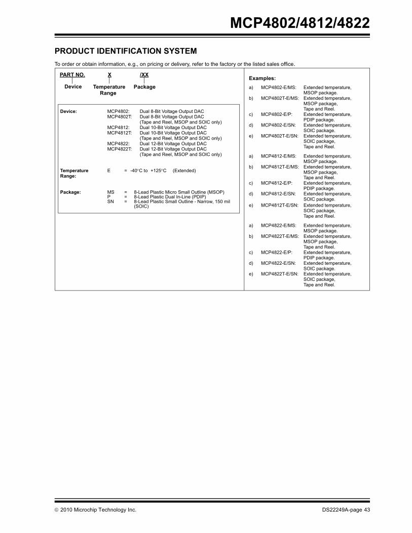
PRODUCT IDENTIFICATION SYSTEMTo order or obtain information, e.g., on pricing or delivery, refer to the factory or the listed sales office.
PART NO. X /XX
PackageTemperatureRange
Device
Device: MCP4802: Dual 8-Bit Voltage Output DACMCP4802T: Dual 8-Bit Voltage Output DAC
(Tape and Reel, MSOP and SOIC only)MCP4812: Dual 10-Bit Voltage Output DACMCP4812T: Dual 10-Bit Voltage Output DAC
(Tape and Reel, MSOP and SOIC only)MCP4822: Dual 12-Bit Voltage Output DACMCP4822T: Dual 12-Bit Voltage Output DAC
(Tape and Reel, MSOP and SOIC only)
Temperature Range:
E = -40C to +125C (Extended)
Package: MS = 8-Lead Plastic Micro Small Outline (MSOP)P = 8-Lead Plastic Dual In-Line (PDIP)SN = 8-Lead Plastic Small Outline - Narrow, 150 mil
(SOIC)
Examples:a) MCP4802-E/MS: Extended temperature,
MSOP package.b) MCP4802T-E/MS: Extended temperature,
MSOP package, Tape and Reel.
c) MCP4802-E/P: Extended temperature,PDIP package.
d) MCP4802-E/SN: Extended temperature,SOIC package.
e) MCP4802T-E/SN: Extended temperature,SOIC package, Tape and Reel.
a) MCP4812-E/MS: Extended temperature,MSOP package.
b) MCP4812T-E/MS: Extended temperature,MSOP package, Tape and Reel.
c) MCP4812-E/P: Extended temperature,PDIP package.
d) MCP4812-E/SN: Extended temperature,SOIC package.
e) MCP4812T-E/SN: Extended temperature,SOIC package, Tape and Reel.
a) MCP4822-E/MS: Extended temperature,MSOP package.
b) MCP4822T-E/MS: Extended temperature,MSOP package, Tape and Reel.
c) MCP4822-E/P: Extended temperature,PDIP package.
d) MCP4822-E/SN: Extended temperature,SOIC package.
e) MCP4822T-E/SN: Extended temperature,SOIC package, Tape and Reel.
2010 Microchip Technology Inc. DS22249A-page 43

MCP4802/4812/4822
NOTES:DS22249A-page 44 2010 Microchip Technology Inc.
Note the following details of the code protection feature on Microchip devices:• Microchip products meet the specification contained in their particular Microchip Data Sheet.
• Microchip believes that its family of products is one of the most secure families of its kind on the market today, when used in the intended manner and under normal conditions.
• There are dishonest and possibly illegal methods used to breach the code protection feature. All of these methods, to our knowledge, require using the Microchip products in a manner outside the operating specifications contained in Microchip’s Data Sheets. Most likely, the person doing so is engaged in theft of intellectual property.
• Microchip is willing to work with the customer who is concerned about the integrity of their code.
• Neither Microchip nor any other semiconductor manufacturer can guarantee the security of their code. Code protection does not mean that we are guaranteeing the product as “unbreakable.”
Code protection is constantly evolving. We at Microchip are committed to continuously improving the code protection features of ourproducts. Attempts to break Microchip’s code protection feature may be a violation of the Digital Millennium Copyright Act. If such actsallow unauthorized access to your software or other copyrighted work, you may have a right to sue for relief under that Act.
Information contained in this publication regarding deviceapplications and the like is provided only for your convenienceand may be superseded by updates. It is your responsibility toensure that your application meets with your specifications.MICROCHIP MAKES NO REPRESENTATIONS ORWARRANTIES OF ANY KIND WHETHER EXPRESS ORIMPLIED, WRITTEN OR ORAL, STATUTORY OROTHERWISE, RELATED TO THE INFORMATION,INCLUDING BUT NOT LIMITED TO ITS CONDITION,QUALITY, PERFORMANCE, MERCHANTABILITY ORFITNESS FOR PURPOSE. Microchip disclaims all liabilityarising from this information and its use. Use of Microchipdevices in life support and/or safety applications is entirely atthe buyer’s risk, and the buyer agrees to defend, indemnify andhold harmless Microchip from any and all damages, claims,suits, or expenses resulting from such use. No licenses areconveyed, implicitly or otherwise, under any Microchipintellectual property rights.
2010 Microchip Technology Inc.
Trademarks
The Microchip name and logo, the Microchip logo, dsPIC, KEELOQ, KEELOQ logo, MPLAB, PIC, PICmicro, PICSTART, PIC32 logo, rfPIC and UNI/O are registered trademarks of Microchip Technology Incorporated in the U.S.A. and other countries.
FilterLab, Hampshire, HI-TECH C, Linear Active Thermistor, MXDEV, MXLAB, SEEVAL and The Embedded Control Solutions Company are registered trademarks of Microchip Technology Incorporated in the U.S.A.
Analog-for-the-Digital Age, Application Maestro, CodeGuard, dsPICDEM, dsPICDEM.net, dsPICworks, dsSPEAK, ECAN, ECONOMONITOR, FanSense, HI-TIDE, In-Circuit Serial Programming, ICSP, Mindi, MiWi, MPASM, MPLAB Certified logo, MPLIB, MPLINK, mTouch, Octopus, Omniscient Code Generation, PICC, PICC-18, PICDEM, PICDEM.net, PICkit, PICtail, REAL ICE, rfLAB, Select Mode, Total Endurance, TSHARC, UniWinDriver, WiperLock and ZENA are trademarks of Microchip Technology Incorporated in the U.S.A. and other countries.
SQTP is a service mark of Microchip Technology Incorporated in the U.S.A.
All other trademarks mentioned herein are property of their respective companies.
© 2010, Microchip Technology Incorporated, Printed in the U.S.A., All Rights Reserved.
Printed on recycled paper.
ISBN: 978-1-60932-128-4
DS22249A-page 45
Microchip received ISO/TS-16949:2002 certification for its worldwide headquarters, design and wafer fabrication facilities in Chandler and Tempe, Arizona; Gresham, Oregon and design centers in California and India. The Company’s quality system processes and procedures are for its PIC® MCUs and dsPIC® DSCs, KEELOQ® code hopping devices, Serial EEPROMs, microperipherals, nonvolatile memory and analog products. In addition, Microchip’s quality system for the design and manufacture of development systems is ISO 9001:2000 certified.
DS22249A-page 46 2010 Microchip Technology Inc.
AMERICASCorporate Office2355 West Chandler Blvd.Chandler, AZ 85224-6199Tel: 480-792-7200 Fax: 480-792-7277Technical Support: http://support.microchip.comWeb Address: www.microchip.comAtlantaDuluth, GA Tel: 678-957-9614 Fax: 678-957-1455BostonWestborough, MA Tel: 774-760-0087 Fax: 774-760-0088ChicagoItasca, IL Tel: 630-285-0071 Fax: 630-285-0075ClevelandIndependence, OH Tel: 216-447-0464 Fax: 216-447-0643DallasAddison, TX Tel: 972-818-7423 Fax: 972-818-2924DetroitFarmington Hills, MI Tel: 248-538-2250Fax: 248-538-2260KokomoKokomo, IN Tel: 765-864-8360Fax: 765-864-8387Los AngelesMission Viejo, CA Tel: 949-462-9523 Fax: 949-462-9608Santa ClaraSanta Clara, CA Tel: 408-961-6444Fax: 408-961-6445TorontoMississauga, Ontario, CanadaTel: 905-673-0699 Fax: 905-673-6509
ASIA/PACIFICAsia Pacific OfficeSuites 3707-14, 37th FloorTower 6, The GatewayHarbour City, KowloonHong KongTel: 852-2401-1200Fax: 852-2401-3431Australia - SydneyTel: 61-2-9868-6733Fax: 61-2-9868-6755China - BeijingTel: 86-10-8528-2100 Fax: 86-10-8528-2104China - ChengduTel: 86-28-8665-5511Fax: 86-28-8665-7889China - ChongqingTel: 86-23-8980-9588Fax: 86-23-8980-9500China - Hong Kong SARTel: 852-2401-1200 Fax: 852-2401-3431China - NanjingTel: 86-25-8473-2460Fax: 86-25-8473-2470China - QingdaoTel: 86-532-8502-7355Fax: 86-532-8502-7205China - ShanghaiTel: 86-21-5407-5533 Fax: 86-21-5407-5066China - ShenyangTel: 86-24-2334-2829Fax: 86-24-2334-2393China - ShenzhenTel: 86-755-8203-2660 Fax: 86-755-8203-1760China - WuhanTel: 86-27-5980-5300Fax: 86-27-5980-5118China - XianTel: 86-29-8833-7252Fax: 86-29-8833-7256China - XiamenTel: 86-592-2388138 Fax: 86-592-2388130China - ZhuhaiTel: 86-756-3210040 Fax: 86-756-3210049
ASIA/PACIFICIndia - BangaloreTel: 91-80-3090-4444 Fax: 91-80-3090-4123India - New DelhiTel: 91-11-4160-8631Fax: 91-11-4160-8632India - PuneTel: 91-20-2566-1512Fax: 91-20-2566-1513Japan - YokohamaTel: 81-45-471- 6166 Fax: 81-45-471-6122Korea - DaeguTel: 82-53-744-4301Fax: 82-53-744-4302Korea - SeoulTel: 82-2-554-7200Fax: 82-2-558-5932 or 82-2-558-5934Malaysia - Kuala LumpurTel: 60-3-6201-9857Fax: 60-3-6201-9859Malaysia - PenangTel: 60-4-227-8870Fax: 60-4-227-4068Philippines - ManilaTel: 63-2-634-9065Fax: 63-2-634-9069SingaporeTel: 65-6334-8870Fax: 65-6334-8850Taiwan - Hsin ChuTel: 886-3-6578-300Fax: 886-3-6578-370Taiwan - KaohsiungTel: 886-7-536-4818Fax: 886-7-536-4803Taiwan - TaipeiTel: 886-2-2500-6610 Fax: 886-2-2508-0102Thailand - BangkokTel: 66-2-694-1351Fax: 66-2-694-1350
EUROPEAustria - WelsTel: 43-7242-2244-39Fax: 43-7242-2244-393Denmark - CopenhagenTel: 45-4450-2828 Fax: 45-4485-2829France - ParisTel: 33-1-69-53-63-20 Fax: 33-1-69-30-90-79Germany - MunichTel: 49-89-627-144-0 Fax: 49-89-627-144-44Italy - Milan Tel: 39-0331-742611 Fax: 39-0331-466781Netherlands - DrunenTel: 31-416-690399 Fax: 31-416-690340Spain - MadridTel: 34-91-708-08-90Fax: 34-91-708-08-91UK - WokinghamTel: 44-118-921-5869Fax: 44-118-921-5820
WORLDWIDE SALES AND SERVICE
01/05/10