Embed Size (px)
Citation preview
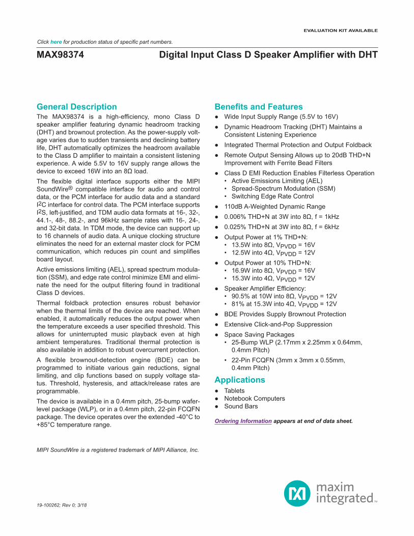
General DescriptionThe MAX98374 is a high-efficiency, mono Class D speaker amplifier featuring dynamic headroom tracking (DHT) and brownout protection. As the power-supply volt-age varies due to sudden transients and declining battery life, DHT automatically optimizes the headroom available to the Class D amplifier to maintain a consistent listening experience. A wide 5.5V to 16V supply range allows the device to exceed 16W into an 8Ω load.The flexible digital interface supports either the MIPI SoundWire® compatible interface for audio and control data, or the PCM interface for audio data and a standard I2C interface for control data. The PCM interface supports I2S, left-justified, and TDM audio data formats at 16-, 32-, 44.1-, 48-, 88.2-, and 96kHz sample rates with 16-, 24-, and 32-bit data. In TDM mode, the device can support up to 16 channels of audio data. A unique clocking structure eliminates the need for an external master clock for PCM communication, which reduces pin count and simplifies board layout.Active emissions limiting (AEL), spread spectrum modula-tion (SSM), and edge rate control minimize EMI and elimi-nate the need for the output filtering found in traditional Class D devices.Thermal foldback protection ensures robust behavior when the thermal limits of the device are reached. When enabled, it automatically reduces the output power when the temperature exceeds a user specified threshold. This allows for uninterrupted music playback even at high ambient temperatures. Traditional thermal protection is also available in addition to robust overcurrent protection. A flexible brownout-detection engine (BDE) can be programmed to initiate various gain reductions, signal limiting, and clip functions based on supply voltage sta-tus. Threshold, hysteresis, and attack/release rates are programmable.The device is available in a 0.4mm pitch, 25-bump wafer-level package (WLP), or in a 0.4mm pitch, 22-pin FCQFN package. The device operates over the extended -40°C to +85°C temperature range.
Benefits and Features Wide Input Supply Range (5.5V to 16V) Dynamic Headroom Tracking (DHT) Maintains a
Consistent Listening Experience Integrated Thermal Protection and Output Foldback Remote Output Sensing Allows up to 20dB THD+N
Improvement with Ferrite Bead Filters Class D EMI Reduction Enables Filterless Operation
• Active Emissions Limiting (AEL)• Spread-Spectrum Modulation (SSM)• Switching Edge Rate Control
110dB A-Weighted Dynamic Range 0.006% THD+N at 3W into 8Ω, f = 1kHz 0.025% THD+N at 3W into 8Ω, f = 6kHz Output Power at 1% THD+N:
• 13.5W into 8Ω, VPVDD = 16V• 12.5W into 4Ω, VPVDD = 12V
Output Power at 10% THD+N:• 16.9W into 8Ω, VPVDD = 16V• 15.3W into 4Ω, VPVDD = 12V
Speaker Amplifier Efficiency:• 90.5% at 10W into 8Ω, VPVDD = 12V• 81% at 15.3W into 4Ω, VPVDD = 12V
BDE Provides Supply Brownout Protection Extensive Click-and-Pop Suppression Space Saving Packages
• 25-Bump WLP (2.17mm x 2.25mm x 0.64mm, 0.4mm Pitch)
• 22-Pin FCQFN (3mm x 3mm x 0.55mm, 0.4mm Pitch)
Applications Tablets Notebook Computers Sound Bars
Ordering Information appears at end of data sheet.
19-100262; Rev 0; 3/18
MIPI SoundWire is a registered trademark of MIPI Alliance, Inc.
MAX98374 Digital Input Class D Speaker Amplifier with DHT
EVALUATION KIT AVAILABLE
Click here for production status of specific part numbers.

Simplified Block Diagram
MAX98374
THERMAL FOLDBACK
BROWNOUT DETECTION
ENGINE
DYNAMIC HEADROOM TRACKING
DACCONTROL AND AUDIO INTERFACES
I2C + PCM INTERFACE
OR SOUNDWIRE INTERFACE
CLASS D
MAX98374 Digital Input Class D Speaker Amplifier with DHT
www.maximintegrated.com Maxim Integrated 2

General Description . . . . . . . . . . . . . . . . . . . . . . . . . . . . . . . . . . . . . . . . . . . . . . . . . . . . . . . . . . . . . . . . . . . . . . . . . . . . 1Benefits and Features . . . . . . . . . . . . . . . . . . . . . . . . . . . . . . . . . . . . . . . . . . . . . . . . . . . . . . . . . . . . . . . . . . . . . . . . . . 1Simplified Block Diagram. . . . . . . . . . . . . . . . . . . . . . . . . . . . . . . . . . . . . . . . . . . . . . . . . . . . . . . . . . . . . . . . . . . . . . . . 2Detailed Block Diagram . . . . . . . . . . . . . . . . . . . . . . . . . . . . . . . . . . . . . . . . . . . . . . . . . . . . . . . . . . . . . . . . . . . . . . . . .11Absolute Maximum Ratings . . . . . . . . . . . . . . . . . . . . . . . . . . . . . . . . . . . . . . . . . . . . . . . . . . . . . . . . . . . . . . . . . . . . . 12Package Thermal Characteristics . . . . . . . . . . . . . . . . . . . . . . . . . . . . . . . . . . . . . . . . . . . . . . . . . . . . . . . . . . . . . . . . 12Electrical Characteristics . . . . . . . . . . . . . . . . . . . . . . . . . . . . . . . . . . . . . . . . . . . . . . . . . . . . . . . . . . . . . . . . . . . . . . . 12PCM and ICC Interface Timing Characteristics. . . . . . . . . . . . . . . . . . . . . . . . . . . . . . . . . . . . . . . . . . . . . . . . . . . . . . 18I2C Interface Timing Characteristics . . . . . . . . . . . . . . . . . . . . . . . . . . . . . . . . . . . . . . . . . . . . . . . . . . . . . . . . . . . . . . 21SoundWire Compatible Slave Interface Timing Characteristics . . . . . . . . . . . . . . . . . . . . . . . . . . . . . . . . . . . . . . . . . 22Device Reset Timing Characteristics . . . . . . . . . . . . . . . . . . . . . . . . . . . . . . . . . . . . . . . . . . . . . . . . . . . . . . . . . . . . . . 24Typical Operating Characteristics . . . . . . . . . . . . . . . . . . . . . . . . . . . . . . . . . . . . . . . . . . . . . . . . . . . . . . . . . . . . . . . . 25Pin Configuration (WLP) . . . . . . . . . . . . . . . . . . . . . . . . . . . . . . . . . . . . . . . . . . . . . . . . . . . . . . . . . . . . . . . . . . . . . . . 36Pin Configuration (FCQFN) . . . . . . . . . . . . . . . . . . . . . . . . . . . . . . . . . . . . . . . . . . . . . . . . . . . . . . . . . . . . . . . . . . . . . 37Pin Description . . . . . . . . . . . . . . . . . . . . . . . . . . . . . . . . . . . . . . . . . . . . . . . . . . . . . . . . . . . . . . . . . . . . . . . . . . . . . . . 38Detailed Description. . . . . . . . . . . . . . . . . . . . . . . . . . . . . . . . . . . . . . . . . . . . . . . . . . . . . . . . . . . . . . . . . . . . . . . . . . . 39
Control Interface Configuration. . . . . . . . . . . . . . . . . . . . . . . . . . . . . . . . . . . . . . . . . . . . . . . . . . . . . . . . . . . . . . . . . 39Device Register Map. . . . . . . . . . . . . . . . . . . . . . . . . . . . . . . . . . . . . . . . . . . . . . . . . . . . . . . . . . . . . . . . . . . . . . . . . 40
Control Bit Field Types and Write Access Restrictions . . . . . . . . . . . . . . . . . . . . . . . . . . . . . . . . . . . . . . . . . . . . 48Device Sequencing . . . . . . . . . . . . . . . . . . . . . . . . . . . . . . . . . . . . . . . . . . . . . . . . . . . . . . . . . . . . . . . . . . . . . . . . . . 49Device State Control . . . . . . . . . . . . . . . . . . . . . . . . . . . . . . . . . . . . . . . . . . . . . . . . . . . . . . . . . . . . . . . . . . . . . . . . . 50
Hardware Shutdown. . . . . . . . . . . . . . . . . . . . . . . . . . . . . . . . . . . . . . . . . . . . . . . . . . . . . . . . . . . . . . . . . . . . . . . 50Software Shutdown . . . . . . . . . . . . . . . . . . . . . . . . . . . . . . . . . . . . . . . . . . . . . . . . . . . . . . . . . . . . . . . . . . . . . . . 50Power Supply UVLO . . . . . . . . . . . . . . . . . . . . . . . . . . . . . . . . . . . . . . . . . . . . . . . . . . . . . . . . . . . . . . . . . . . . . . 50Software Reset . . . . . . . . . . . . . . . . . . . . . . . . . . . . . . . . . . . . . . . . . . . . . . . . . . . . . . . . . . . . . . . . . . . . . . . . . . 50SoundWire Bus Reset . . . . . . . . . . . . . . . . . . . . . . . . . . . . . . . . . . . . . . . . . . . . . . . . . . . . . . . . . . . . . . . . . . . . . 50SoundWire Register Reset . . . . . . . . . . . . . . . . . . . . . . . . . . . . . . . . . . . . . . . . . . . . . . . . . . . . . . . . . . . . . . . . . 50
Global Enable . . . . . . . . . . . . . . . . . . . . . . . . . . . . . . . . . . . . . . . . . . . . . . . . . . . . . . . . . . . . . . . . . . . . . . . . . . . . . . 51Software Reset . . . . . . . . . . . . . . . . . . . . . . . . . . . . . . . . . . . . . . . . . . . . . . . . . . . . . . . . . . . . . . . . . . . . . . . . . . . . . 51I2C Serial Interface . . . . . . . . . . . . . . . . . . . . . . . . . . . . . . . . . . . . . . . . . . . . . . . . . . . . . . . . . . . . . . . . . . . . . . . . . . 52
I2C Slave Address . . . . . . . . . . . . . . . . . . . . . . . . . . . . . . . . . . . . . . . . . . . . . . . . . . . . . . . . . . . . . . . . . . . . . . . . 52I2C Slave Interface Operation . . . . . . . . . . . . . . . . . . . . . . . . . . . . . . . . . . . . . . . . . . . . . . . . . . . . . . . . . . . . . . . 52Bit Transfer. . . . . . . . . . . . . . . . . . . . . . . . . . . . . . . . . . . . . . . . . . . . . . . . . . . . . . . . . . . . . . . . . . . . . . . . . . . . . . 52START and STOP Conditions . . . . . . . . . . . . . . . . . . . . . . . . . . . . . . . . . . . . . . . . . . . . . . . . . . . . . . . . . . . . . . . 53Early STOP Conditions . . . . . . . . . . . . . . . . . . . . . . . . . . . . . . . . . . . . . . . . . . . . . . . . . . . . . . . . . . . . . . . . . . . . 53
TABLE OF CONTENTS
MAX98374 Digital Input Class D Speaker Amplifier with DHT
www.maximintegrated.com Maxim Integrated 3
Acknowledge . . . . . . . . . . . . . . . . . . . . . . . . . . . . . . . . . . . . . . . . . . . . . . . . . . . . . . . . . . . . . . . . . . . . . . . . . . . . 53I2C Write Data Format . . . . . . . . . . . . . . . . . . . . . . . . . . . . . . . . . . . . . . . . . . . . . . . . . . . . . . . . . . . . . . . . . . . . . 54I2C Read Data Format . . . . . . . . . . . . . . . . . . . . . . . . . . . . . . . . . . . . . . . . . . . . . . . . . . . . . . . . . . . . . . . . . . . . . 55
Audio Interface Mode Configuration. . . . . . . . . . . . . . . . . . . . . . . . . . . . . . . . . . . . . . . . . . . . . . . . . . . . . . . . . . . . . 56PCM Interface . . . . . . . . . . . . . . . . . . . . . . . . . . . . . . . . . . . . . . . . . . . . . . . . . . . . . . . . . . . . . . . . . . . . . . . . . . . . . . 56
PCM Clock Configuration . . . . . . . . . . . . . . . . . . . . . . . . . . . . . . . . . . . . . . . . . . . . . . . . . . . . . . . . . . . . . . . . . . 56Clock Ratio Configuration . . . . . . . . . . . . . . . . . . . . . . . . . . . . . . . . . . . . . . . . . . . . . . . . . . . . . . . . . . . . . . . . . . 56
PCM Interface Sample Rate . . . . . . . . . . . . . . . . . . . . . . . . . . . . . . . . . . . . . . . . . . . . . . . . . . . . . . . . . . . . . . . . . . . 57Speaker Path Sample Rate. . . . . . . . . . . . . . . . . . . . . . . . . . . . . . . . . . . . . . . . . . . . . . . . . . . . . . . . . . . . . . . . . . . . 57PCM Interface Clock Ratio Configuration. . . . . . . . . . . . . . . . . . . . . . . . . . . . . . . . . . . . . . . . . . . . . . . . . . . . . . . . . 58
PCM Data Format Configuration . . . . . . . . . . . . . . . . . . . . . . . . . . . . . . . . . . . . . . . . . . . . . . . . . . . . . . . . . . . . . 58I2S and Left-Justified Mode. . . . . . . . . . . . . . . . . . . . . . . . . . . . . . . . . . . . . . . . . . . . . . . . . . . . . . . . . . . . . . . . . 58TDM Modes . . . . . . . . . . . . . . . . . . . . . . . . . . . . . . . . . . . . . . . . . . . . . . . . . . . . . . . . . . . . . . . . . . . . . . . . . . . . . 60
PCM Interface Data Format Configuration . . . . . . . . . . . . . . . . . . . . . . . . . . . . . . . . . . . . . . . . . . . . . . . . . . . . . . . . 62PCM Data Path Configuration . . . . . . . . . . . . . . . . . . . . . . . . . . . . . . . . . . . . . . . . . . . . . . . . . . . . . . . . . . . . . . . 63PCM Data Input . . . . . . . . . . . . . . . . . . . . . . . . . . . . . . . . . . . . . . . . . . . . . . . . . . . . . . . . . . . . . . . . . . . . . . . . . . 63
PCM Interface Data Input (DIN) Enable . . . . . . . . . . . . . . . . . . . . . . . . . . . . . . . . . . . . . . . . . . . . . . . . . . . . . . . . . . 64PCM Interface Digital Mono Mixer Configuration 1 . . . . . . . . . . . . . . . . . . . . . . . . . . . . . . . . . . . . . . . . . . . . . . . . . 64
PCM Data Output. . . . . . . . . . . . . . . . . . . . . . . . . . . . . . . . . . . . . . . . . . . . . . . . . . . . . . . . . . . . . . . . . . . . . . . . . 65PCM Interface Digital Mono Mixer Configuration 2 . . . . . . . . . . . . . . . . . . . . . . . . . . . . . . . . . . . . . . . . . . . . . . . . . 65PCM Interface Data Output (DOUT) Enable . . . . . . . . . . . . . . . . . . . . . . . . . . . . . . . . . . . . . . . . . . . . . . . . . . . . . . 66PCM Interface Data Output Speaker DSP Feedback Channel Source . . . . . . . . . . . . . . . . . . . . . . . . . . . . . . . . . . 66PCM Interface Data Output Channel Configuration 1 . . . . . . . . . . . . . . . . . . . . . . . . . . . . . . . . . . . . . . . . . . . . . . . 67PCM Interface Data Output Channel Configuration 2 . . . . . . . . . . . . . . . . . . . . . . . . . . . . . . . . . . . . . . . . . . . . . . . 68SoundWire Slave Interface . . . . . . . . . . . . . . . . . . . . . . . . . . . . . . . . . . . . . . . . . . . . . . . . . . . . . . . . . . . . . . . . . . . . 69
SoundWire Slave Device Identification and Addressing . . . . . . . . . . . . . . . . . . . . . . . . . . . . . . . . . . . . . . . . . . . 69SoundWire Input Clock Configuration . . . . . . . . . . . . . . . . . . . . . . . . . . . . . . . . . . . . . . . . . . . . . . . . . . . . . . . . . . . 70
SoundWire Clock Configuration . . . . . . . . . . . . . . . . . . . . . . . . . . . . . . . . . . . . . . . . . . . . . . . . . . . . . . . . . . . . . 70SoundWire Slave Control Port (SCP) Configuration . . . . . . . . . . . . . . . . . . . . . . . . . . . . . . . . . . . . . . . . . . . . . . 71SoundWire Device Data Port (DP) Configuration . . . . . . . . . . . . . . . . . . . . . . . . . . . . . . . . . . . . . . . . . . . . . . . . 71
IRQ Bus Configuration . . . . . . . . . . . . . . . . . . . . . . . . . . . . . . . . . . . . . . . . . . . . . . . . . . . . . . . . . . . . . . . . . . . . . . . 72Interrupts . . . . . . . . . . . . . . . . . . . . . . . . . . . . . . . . . . . . . . . . . . . . . . . . . . . . . . . . . . . . . . . . . . . . . . . . . . . . . . . . . . 72
TABLE OF CONTENTS (CONTINUED)
MAX98374 Digital Input Class D Speaker Amplifier with DHT
www.maximintegrated.com Maxim Integrated 4

Interrupt Bit Field Composition . . . . . . . . . . . . . . . . . . . . . . . . . . . . . . . . . . . . . . . . . . . . . . . . . . . . . . . . . . . . . . 72Raw Status (RAW). . . . . . . . . . . . . . . . . . . . . . . . . . . . . . . . . . . . . . . . . . . . . . . . . . . . . . . . . . . . . . . . . . . . . . . . 72State (STATE) . . . . . . . . . . . . . . . . . . . . . . . . . . . . . . . . . . . . . . . . . . . . . . . . . . . . . . . . . . . . . . . . . . . . . . . . . . . 72Flag (FLAG) . . . . . . . . . . . . . . . . . . . . . . . . . . . . . . . . . . . . . . . . . . . . . . . . . . . . . . . . . . . . . . . . . . . . . . . . . . . . . 72Enable (EN) . . . . . . . . . . . . . . . . . . . . . . . . . . . . . . . . . . . . . . . . . . . . . . . . . . . . . . . . . . . . . . . . . . . . . . . . . . . . . 72Clear (CLR) . . . . . . . . . . . . . . . . . . . . . . . . . . . . . . . . . . . . . . . . . . . . . . . . . . . . . . . . . . . . . . . . . . . . . . . . . . . . . 72IRQ Output Configuration . . . . . . . . . . . . . . . . . . . . . . . . . . . . . . . . . . . . . . . . . . . . . . . . . . . . . . . . . . . . . . . . . . 72Interrupt Sources . . . . . . . . . . . . . . . . . . . . . . . . . . . . . . . . . . . . . . . . . . . . . . . . . . . . . . . . . . . . . . . . . . . . . . . . . 72
Device Interrupt Sources . . . . . . . . . . . . . . . . . . . . . . . . . . . . . . . . . . . . . . . . . . . . . . . . . . . . . . . . . . . . . . . . . . . . . 73Digital Output Pin Drive Strength Configuration. . . . . . . . . . . . . . . . . . . . . . . . . . . . . . . . . . . . . . . . . . . . . . . . . . . . 74Digital Output Pin Drive Strength . . . . . . . . . . . . . . . . . . . . . . . . . . . . . . . . . . . . . . . . . . . . . . . . . . . . . . . . . . . . . . . 74Tone Generator . . . . . . . . . . . . . . . . . . . . . . . . . . . . . . . . . . . . . . . . . . . . . . . . . . . . . . . . . . . . . . . . . . . . . . . . . . . . . 75Tone Generator Configuration . . . . . . . . . . . . . . . . . . . . . . . . . . . . . . . . . . . . . . . . . . . . . . . . . . . . . . . . . . . . . . . . . 75Speaker Path Configuration . . . . . . . . . . . . . . . . . . . . . . . . . . . . . . . . . . . . . . . . . . . . . . . . . . . . . . . . . . . . . . . . . . . 76
Speaker Path Dither. . . . . . . . . . . . . . . . . . . . . . . . . . . . . . . . . . . . . . . . . . . . . . . . . . . . . . . . . . . . . . . . . . . . . . . 76Speaker Path Data Inversion . . . . . . . . . . . . . . . . . . . . . . . . . . . . . . . . . . . . . . . . . . . . . . . . . . . . . . . . . . . . . . . . 76Speaker Path DC Blocking Filter . . . . . . . . . . . . . . . . . . . . . . . . . . . . . . . . . . . . . . . . . . . . . . . . . . . . . . . . . . . . . 76Speaker Path Digital Volume Control . . . . . . . . . . . . . . . . . . . . . . . . . . . . . . . . . . . . . . . . . . . . . . . . . . . . . . . . . 76Speaker Path Digital Gain Control. . . . . . . . . . . . . . . . . . . . . . . . . . . . . . . . . . . . . . . . . . . . . . . . . . . . . . . . . . . . 77Speaker Path DSP Data Feedback Path. . . . . . . . . . . . . . . . . . . . . . . . . . . . . . . . . . . . . . . . . . . . . . . . . . . . . . . 77Speaker Path Maximum Peak Output-Voltage Scaling . . . . . . . . . . . . . . . . . . . . . . . . . . . . . . . . . . . . . . . . . . . . 77
Speaker Path DSP Configuration . . . . . . . . . . . . . . . . . . . . . . . . . . . . . . . . . . . . . . . . . . . . . . . . . . . . . . . . . . . . . . . 78Speaker Path Digital Volume Control . . . . . . . . . . . . . . . . . . . . . . . . . . . . . . . . . . . . . . . . . . . . . . . . . . . . . . . . . . . . 79Speaker Path Output Level Scaling . . . . . . . . . . . . . . . . . . . . . . . . . . . . . . . . . . . . . . . . . . . . . . . . . . . . . . . . . . . . . 79Class D Speaker Amplifier Output Stage . . . . . . . . . . . . . . . . . . . . . . . . . . . . . . . . . . . . . . . . . . . . . . . . . . . . . . . . . 80
Speaker Amplifier Clock Synchronization . . . . . . . . . . . . . . . . . . . . . . . . . . . . . . . . . . . . . . . . . . . . . . . . . . . . . . 80Speaker Amplifier Ultra-Low EMI Filterless Operation . . . . . . . . . . . . . . . . . . . . . . . . . . . . . . . . . . . . . . . . . . . . 80Speaker Amplifier Current Limit. . . . . . . . . . . . . . . . . . . . . . . . . . . . . . . . . . . . . . . . . . . . . . . . . . . . . . . . . . . . . . 80
Speaker Path and Speaker DSP Data Feedback Path Enables . . . . . . . . . . . . . . . . . . . . . . . . . . . . . . . . . . . . . . . 81Speaker Amplifier Switching Edge Rate Configuration . . . . . . . . . . . . . . . . . . . . . . . . . . . . . . . . . . . . . . . . . . . . . . 81Speaker Amplifier Configuration. . . . . . . . . . . . . . . . . . . . . . . . . . . . . . . . . . . . . . . . . . . . . . . . . . . . . . . . . . . . . . . . 82
TABLE OF CONTENTS (CONTINUED)
MAX98374 Digital Input Class D Speaker Amplifier with DHT
www.maximintegrated.com Maxim Integrated 5

Measurement ADC . . . . . . . . . . . . . . . . . . . . . . . . . . . . . . . . . . . . . . . . . . . . . . . . . . . . . . . . . . . . . . . . . . . . . . . . . . 82Measurement ADC Thermal Channel . . . . . . . . . . . . . . . . . . . . . . . . . . . . . . . . . . . . . . . . . . . . . . . . . . . . . . . . . 82Measurement ADC Thermal Channel . . . . . . . . . . . . . . . . . . . . . . . . . . . . . . . . . . . . . . . . . . . . . . . . . . . . . . . . . 83
Measurement ADC Sample Rate Control. . . . . . . . . . . . . . . . . . . . . . . . . . . . . . . . . . . . . . . . . . . . . . . . . . . . . . . . . 83Measurement ADC Thermal Channel Readback . . . . . . . . . . . . . . . . . . . . . . . . . . . . . . . . . . . . . . . . . . . . . . . . . . . 83Measurement ADC Thermal Channel Filter Configuration. . . . . . . . . . . . . . . . . . . . . . . . . . . . . . . . . . . . . . . . . . . . 84
Measurement ADC PVDD Channel. . . . . . . . . . . . . . . . . . . . . . . . . . . . . . . . . . . . . . . . . . . . . . . . . . . . . . . . . . . 84Measurement ADC PVDD Channel Readback. . . . . . . . . . . . . . . . . . . . . . . . . . . . . . . . . . . . . . . . . . . . . . . . . . . . . 85Measurement ADC PVDD Channel Filter Configuration . . . . . . . . . . . . . . . . . . . . . . . . . . . . . . . . . . . . . . . . . . . . . 85Measurement ADC PVDD Channel Enable . . . . . . . . . . . . . . . . . . . . . . . . . . . . . . . . . . . . . . . . . . . . . . . . . . . . . . . 86Clock Monitor . . . . . . . . . . . . . . . . . . . . . . . . . . . . . . . . . . . . . . . . . . . . . . . . . . . . . . . . . . . . . . . . . . . . . . . . . . . . . . 86
Clock Monitor in SoundWire Control Mode . . . . . . . . . . . . . . . . . . . . . . . . . . . . . . . . . . . . . . . . . . . . . . . . . . . . . 86Device Auto-Restart Configuration. . . . . . . . . . . . . . . . . . . . . . . . . . . . . . . . . . . . . . . . . . . . . . . . . . . . . . . . . . . . . . 87Dynamic Headroom Tracking (DHT). . . . . . . . . . . . . . . . . . . . . . . . . . . . . . . . . . . . . . . . . . . . . . . . . . . . . . . . . . . . . 88DHT Modes of Operation . . . . . . . . . . . . . . . . . . . . . . . . . . . . . . . . . . . . . . . . . . . . . . . . . . . . . . . . . . . . . . . . . . . . . 88
MODE 1: VPVDD is greater than VMPO. . . . . . . . . . . . . . . . . . . . . . . . . . . . . . . . . . . . . . . . . . . . . . . . . . . . . . . . 88MODE 2: VPVDD is less than VMPO and greater than VRP . . . . . . . . . . . . . . . . . . . . . . . . . . . . . . . . . . . . . . . . 89MODE 3a: VPVDD is less than VRP and greater than VMIN . . . . . . . . . . . . . . . . . . . . . . . . . . . . . . . . . . . . . . . . 89MODE 3b: VPVDD is less than VMIN and greater than VRP . . . . . . . . . . . . . . . . . . . . . . . . . . . . . . . . . . . . . . . . 91
DHT Enable. . . . . . . . . . . . . . . . . . . . . . . . . . . . . . . . . . . . . . . . . . . . . . . . . . . . . . . . . . . . . . . . . . . . . . . . . . . . . . . . 92DHT Ballistics. . . . . . . . . . . . . . . . . . . . . . . . . . . . . . . . . . . . . . . . . . . . . . . . . . . . . . . . . . . . . . . . . . . . . . . . . . . . 93
DHT Configuration . . . . . . . . . . . . . . . . . . . . . . . . . . . . . . . . . . . . . . . . . . . . . . . . . . . . . . . . . . . . . . . . . . . . . . . . . . 93DHT Headroom Calculation. . . . . . . . . . . . . . . . . . . . . . . . . . . . . . . . . . . . . . . . . . . . . . . . . . . . . . . . . . . . . . . . . 94
DHT Attack Rate Settings. . . . . . . . . . . . . . . . . . . . . . . . . . . . . . . . . . . . . . . . . . . . . . . . . . . . . . . . . . . . . . . . . . . . . 95DHT Release Rate Settings . . . . . . . . . . . . . . . . . . . . . . . . . . . . . . . . . . . . . . . . . . . . . . . . . . . . . . . . . . . . . . . . . . . 95Limiter . . . . . . . . . . . . . . . . . . . . . . . . . . . . . . . . . . . . . . . . . . . . . . . . . . . . . . . . . . . . . . . . . . . . . . . . . . . . . . . . . . . . 96Limiter Enable . . . . . . . . . . . . . . . . . . . . . . . . . . . . . . . . . . . . . . . . . . . . . . . . . . . . . . . . . . . . . . . . . . . . . . . . . . . . . . 97Limiter Threshold Configuration . . . . . . . . . . . . . . . . . . . . . . . . . . . . . . . . . . . . . . . . . . . . . . . . . . . . . . . . . . . . . . . . 97Limiter Attack and Release Rate Configuration . . . . . . . . . . . . . . . . . . . . . . . . . . . . . . . . . . . . . . . . . . . . . . . . . . . . 98Brownout-Detection Engine (BDE) . . . . . . . . . . . . . . . . . . . . . . . . . . . . . . . . . . . . . . . . . . . . . . . . . . . . . . . . . . . . . . 99
BDE State Controller and Level Thresholds . . . . . . . . . . . . . . . . . . . . . . . . . . . . . . . . . . . . . . . . . . . . . . . . . . . . 99BDE Level Configuration Options . . . . . . . . . . . . . . . . . . . . . . . . . . . . . . . . . . . . . . . . . . . . . . . . . . . . . . . . . . . 101
TABLE OF CONTENTS (CONTINUED)
MAX98374 Digital Input Class D Speaker Amplifier with DHT
www.maximintegrated.com Maxim Integrated 6

BDE Gain Reduction. . . . . . . . . . . . . . . . . . . . . . . . . . . . . . . . . . . . . . . . . . . . . . . . . . . . . . . . . . . . . . . . . . . . . . . . 101BDE Limiter Function . . . . . . . . . . . . . . . . . . . . . . . . . . . . . . . . . . . . . . . . . . . . . . . . . . . . . . . . . . . . . . . . . . . . . 102BDE Clipper Function . . . . . . . . . . . . . . . . . . . . . . . . . . . . . . . . . . . . . . . . . . . . . . . . . . . . . . . . . . . . . . . . . . . . 102
BDE Current State . . . . . . . . . . . . . . . . . . . . . . . . . . . . . . . . . . . . . . . . . . . . . . . . . . . . . . . . . . . . . . . . . . . . . . . . . 103BDE Level Hold Time . . . . . . . . . . . . . . . . . . . . . . . . . . . . . . . . . . . . . . . . . . . . . . . . . . . . . . . . . . . . . . . . . . . . . . . 104BDE Enable. . . . . . . . . . . . . . . . . . . . . . . . . . . . . . . . . . . . . . . . . . . . . . . . . . . . . . . . . . . . . . . . . . . . . . . . . . . . . . . 104BDE Level 1 Threshold . . . . . . . . . . . . . . . . . . . . . . . . . . . . . . . . . . . . . . . . . . . . . . . . . . . . . . . . . . . . . . . . . . . . . . 104BDE Level 2 Threshold . . . . . . . . . . . . . . . . . . . . . . . . . . . . . . . . . . . . . . . . . . . . . . . . . . . . . . . . . . . . . . . . . . . . . . 105BDE Level 3 Threshold . . . . . . . . . . . . . . . . . . . . . . . . . . . . . . . . . . . . . . . . . . . . . . . . . . . . . . . . . . . . . . . . . . . . . . 105BDE Level 4 Threshold . . . . . . . . . . . . . . . . . . . . . . . . . . . . . . . . . . . . . . . . . . . . . . . . . . . . . . . . . . . . . . . . . . . . . . 106BDE Level Threshold Hysteresis . . . . . . . . . . . . . . . . . . . . . . . . . . . . . . . . . . . . . . . . . . . . . . . . . . . . . . . . . . . . . . 106BDE Gain Reduction Attack/Release Rates. . . . . . . . . . . . . . . . . . . . . . . . . . . . . . . . . . . . . . . . . . . . . . . . . . . . . . 107BDE Clipper Mode . . . . . . . . . . . . . . . . . . . . . . . . . . . . . . . . . . . . . . . . . . . . . . . . . . . . . . . . . . . . . . . . . . . . . . . . . 108BDE Level 1 Limiter Configuration . . . . . . . . . . . . . . . . . . . . . . . . . . . . . . . . . . . . . . . . . . . . . . . . . . . . . . . . . . . . . 108BDE Level 1 Clipper Configuration. . . . . . . . . . . . . . . . . . . . . . . . . . . . . . . . . . . . . . . . . . . . . . . . . . . . . . . . . . . . . 109BDE Level 1 Gain Reduction Configuration . . . . . . . . . . . . . . . . . . . . . . . . . . . . . . . . . . . . . . . . . . . . . . . . . . . . . . 109BDE Level 2 Limiter Configuration . . . . . . . . . . . . . . . . . . . . . . . . . . . . . . . . . . . . . . . . . . . . . . . . . . . . . . . . . . . . . 110BDE Level 2 Clipper Configuration. . . . . . . . . . . . . . . . . . . . . . . . . . . . . . . . . . . . . . . . . . . . . . . . . . . . . . . . . . . . . 110BDE Level 2 Gain Reduction Configuration . . . . . . . . . . . . . . . . . . . . . . . . . . . . . . . . . . . . . . . . . . . . . . . . . . . . . . 111BDE Level 3 Limiter Configuration . . . . . . . . . . . . . . . . . . . . . . . . . . . . . . . . . . . . . . . . . . . . . . . . . . . . . . . . . . . . . 111BDE Level 3 Clipper Configuration. . . . . . . . . . . . . . . . . . . . . . . . . . . . . . . . . . . . . . . . . . . . . . . . . . . . . . . . . . . . . 112BDE Level 3 Gain Reduction Configuration . . . . . . . . . . . . . . . . . . . . . . . . . . . . . . . . . . . . . . . . . . . . . . . . . . . . . . 112BDE Level 4 Limiter Configuration . . . . . . . . . . . . . . . . . . . . . . . . . . . . . . . . . . . . . . . . . . . . . . . . . . . . . . . . . . . . . 113BDE Level 4 Clipper and State Configuration . . . . . . . . . . . . . . . . . . . . . . . . . . . . . . . . . . . . . . . . . . . . . . . . . . . . 113BDE Level 4 Gain Reduction Configuration . . . . . . . . . . . . . . . . . . . . . . . . . . . . . . . . . . . . . . . . . . . . . . . . . . . . . . 114BDE Level 4 Infinite Hold Clear . . . . . . . . . . . . . . . . . . . . . . . . . . . . . . . . . . . . . . . . . . . . . . . . . . . . . . . . . . . . . . . 114Thermal Protection . . . . . . . . . . . . . . . . . . . . . . . . . . . . . . . . . . . . . . . . . . . . . . . . . . . . . . . . . . . . . . . . . . . . . . . . . 115
Thermal Warning and Shutdown Threshold Configuration . . . . . . . . . . . . . . . . . . . . . . . . . . . . . . . . . . . . . . . . 115
TABLE OF CONTENTS (CONTINUED)
MAX98374 Digital Input Class D Speaker Amplifier with DHT
www.maximintegrated.com Maxim Integrated 7

Thermal-Warning Threshold Configuration . . . . . . . . . . . . . . . . . . . . . . . . . . . . . . . . . . . . . . . . . . . . . . . . . . . . . . 115Thermal-Shutdown Threshold Configuration . . . . . . . . . . . . . . . . . . . . . . . . . . . . . . . . . . . . . . . . . . . . . . . . . . . . . 115Thermal Hysteresis Configuration . . . . . . . . . . . . . . . . . . . . . . . . . . . . . . . . . . . . . . . . . . . . . . . . . . . . . . . . . . . . . 116
Thermal Shutdown Recovery Configuration . . . . . . . . . . . . . . . . . . . . . . . . . . . . . . . . . . . . . . . . . . . . . . . . . . . 116Thermal Foldback Configuration . . . . . . . . . . . . . . . . . . . . . . . . . . . . . . . . . . . . . . . . . . . . . . . . . . . . . . . . . . . . 116
Thermal-Foldback Settings. . . . . . . . . . . . . . . . . . . . . . . . . . . . . . . . . . . . . . . . . . . . . . . . . . . . . . . . . . . . . . . . . . . 117Thermal-Foldback Enable. . . . . . . . . . . . . . . . . . . . . . . . . . . . . . . . . . . . . . . . . . . . . . . . . . . . . . . . . . . . . . . . . . . . 117ICC Interface. . . . . . . . . . . . . . . . . . . . . . . . . . . . . . . . . . . . . . . . . . . . . . . . . . . . . . . . . . . . . . . . . . . . . . . . . . . . . . 118
ICC Interface Data Format. . . . . . . . . . . . . . . . . . . . . . . . . . . . . . . . . . . . . . . . . . . . . . . . . . . . . . . . . . . . . . . . . 118ICC Interface Device Group Assignment . . . . . . . . . . . . . . . . . . . . . . . . . . . . . . . . . . . . . . . . . . . . . . . . . . . . . 118ICC Data Transmit and Receive . . . . . . . . . . . . . . . . . . . . . . . . . . . . . . . . . . . . . . . . . . . . . . . . . . . . . . . . . . . . 118ICC Interface Group Data Synchronization. . . . . . . . . . . . . . . . . . . . . . . . . . . . . . . . . . . . . . . . . . . . . . . . . . . . 119ICC Interface Link Synchronization . . . . . . . . . . . . . . . . . . . . . . . . . . . . . . . . . . . . . . . . . . . . . . . . . . . . . . . . . . 119
ICC Data Link Configuration . . . . . . . . . . . . . . . . . . . . . . . . . . . . . . . . . . . . . . . . . . . . . . . . . . . . . . . . . . . . . . . . . . 121ICC Receiver Enables 1 . . . . . . . . . . . . . . . . . . . . . . . . . . . . . . . . . . . . . . . . . . . . . . . . . . . . . . . . . . . . . . . . . . . . . 122ICC Receiver Enables 2 . . . . . . . . . . . . . . . . . . . . . . . . . . . . . . . . . . . . . . . . . . . . . . . . . . . . . . . . . . . . . . . . . . . . . 123ICC Transmitter Configuration . . . . . . . . . . . . . . . . . . . . . . . . . . . . . . . . . . . . . . . . . . . . . . . . . . . . . . . . . . . . . . . . 123ICC Transmitter Channel Configuration 1. . . . . . . . . . . . . . . . . . . . . . . . . . . . . . . . . . . . . . . . . . . . . . . . . . . . . . . . 124ICC Transmitter Channel Configuration 2. . . . . . . . . . . . . . . . . . . . . . . . . . . . . . . . . . . . . . . . . . . . . . . . . . . . . . . . 125ICC Transmitter Enable. . . . . . . . . . . . . . . . . . . . . . . . . . . . . . . . . . . . . . . . . . . . . . . . . . . . . . . . . . . . . . . . . . . . . . 125Layout and Grounding. . . . . . . . . . . . . . . . . . . . . . . . . . . . . . . . . . . . . . . . . . . . . . . . . . . . . . . . . . . . . . . . . . . . . . . 126WLP Applications Information. . . . . . . . . . . . . . . . . . . . . . . . . . . . . . . . . . . . . . . . . . . . . . . . . . . . . . . . . . . . . . . . . 126
Typical Application Circuit . . . . . . . . . . . . . . . . . . . . . . . . . . . . . . . . . . . . . . . . . . . . . . . . . . . . . . . . . . . . . . . . . . . . . 127Device Revision Identification Number. . . . . . . . . . . . . . . . . . . . . . . . . . . . . . . . . . . . . . . . . . . . . . . . . . . . . . . . . . 128
Ordering Information . . . . . . . . . . . . . . . . . . . . . . . . . . . . . . . . . . . . . . . . . . . . . . . . . . . . . . . . . . . . . . . . . . . . . . . . . 128Chip Information. . . . . . . . . . . . . . . . . . . . . . . . . . . . . . . . . . . . . . . . . . . . . . . . . . . . . . . . . . . . . . . . . . . . . . . . . . . . . 128Package Information . . . . . . . . . . . . . . . . . . . . . . . . . . . . . . . . . . . . . . . . . . . . . . . . . . . . . . . . . . . . . . . . . . . . . . . . . 128
Revision Identification Number . . . . . . . . . . . . . . . . . . . . . . . . . . . . . . . . . . . . . . . . . . . . . . . . . . . . . . . . . . . . . . . . 128Revision History . . . . . . . . . . . . . . . . . . . . . . . . . . . . . . . . . . . . . . . . . . . . . . . . . . . . . . . . . . . . . . . . . . . . . . . . . . . . . 129
TABLE OF CONTENTS (CONTINUED)
MAX98374 Digital Input Class D Speaker Amplifier with DHT
www.maximintegrated.com Maxim Integrated 8

Figure 1. I2S Audio Interface Timing Diagram. . . . . . . . . . . . . . . . . . . . . . . . . . . . . . . . . . . . . . . . . . . . . . . . . . . . . . . 20Figure 2. Left-Justified Audio Interface Timing Diagram. . . . . . . . . . . . . . . . . . . . . . . . . . . . . . . . . . . . . . . . . . . . . . . 20Figure 3. TDM Interface Timing Diagram . . . . . . . . . . . . . . . . . . . . . . . . . . . . . . . . . . . . . . . . . . . . . . . . . . . . . . . . . . 20Figure 4: PCM Data Output Timing (DOUT) . . . . . . . . . . . . . . . . . . . . . . . . . . . . . . . . . . . . . . . . . . . . . . . . . . . . . . . . 20Figure 5. I2C Timing. . . . . . . . . . . . . . . . . . . . . . . . . . . . . . . . . . . . . . . . . . . . . . . . . . . . . . . . . . . . . . . . . . . . . . . . . . . 21Figure 6. SoundWire Data Input Timing Diagram . . . . . . . . . . . . . . . . . . . . . . . . . . . . . . . . . . . . . . . . . . . . . . . . . . . . 22Figure 7. SoundWire Data Output Timing Diagram . . . . . . . . . . . . . . . . . . . . . . . . . . . . . . . . . . . . . . . . . . . . . . . . . . . 23Figure 8. RESET Timing Diagram . . . . . . . . . . . . . . . . . . . . . . . . . . . . . . . . . . . . . . . . . . . . . . . . . . . . . . . . . . . . . . . . 24Figure 9. Control Interface Configuration Options. . . . . . . . . . . . . . . . . . . . . . . . . . . . . . . . . . . . . . . . . . . . . . . . . . . . 39Figure 10. START, STOP, and REPEATED START Conditions . . . . . . . . . . . . . . . . . . . . . . . . . . . . . . . . . . . . . . . . . 53Figure 11. Acknowledge . . . . . . . . . . . . . . . . . . . . . . . . . . . . . . . . . . . . . . . . . . . . . . . . . . . . . . . . . . . . . . . . . . . . . . . . 53Figure 12. Writing One Byte of Data to the Slave . . . . . . . . . . . . . . . . . . . . . . . . . . . . . . . . . . . . . . . . . . . . . . . . . . . . 54Figure 13. Writing n-Bytes of Data to the Slave . . . . . . . . . . . . . . . . . . . . . . . . . . . . . . . . . . . . . . . . . . . . . . . . . . . . . 54Figure 14. Reading One Byte of Data from the Slave . . . . . . . . . . . . . . . . . . . . . . . . . . . . . . . . . . . . . . . . . . . . . . . . . 55Figure 15. Reading n-Bytes of Data from the Slave . . . . . . . . . . . . . . . . . . . . . . . . . . . . . . . . . . . . . . . . . . . . . . . . . . 55Figure 16. Standard I2S Mode Data Format Example (16-Bit Data Word, 24-Bit Channel Length) . . . . . . . . . . . . . . 59Figure 17. Left-Justified Mode Data Format Examples (16-Bit Data Word, 24-Bit Channel Length) . . . . . . . . . . . . . 59Figure 18. TDM Mode Data Format Examples (4 Channels, 32-Bit Data Word and Channel Length). . . . . . . . . . . . 61Figure 19. Device Signal Path Diagram. . . . . . . . . . . . . . . . . . . . . . . . . . . . . . . . . . . . . . . . . . . . . . . . . . . . . . . . . . . . 63Figure 20. Digital Monomix Control . . . . . . . . . . . . . . . . . . . . . . . . . . . . . . . . . . . . . . . . . . . . . . . . . . . . . . . . . . . . . . . 63Figure 21. Internal Clock Generation in SoundWire Control Mode . . . . . . . . . . . . . . . . . . . . . . . . . . . . . . . . . . . . . . . 70Figure 22. Speaker Path Block Diagram . . . . . . . . . . . . . . . . . . . . . . . . . . . . . . . . . . . . . . . . . . . . . . . . . . . . . . . . . . . 76Figure 23. Filterless EMI results for EN 55022 Class B Standard . . . . . . . . . . . . . . . . . . . . . . . . . . . . . . . . . . . . . . . 80Figure 24. Output EMI results for EN 55022 Class B Standard . . . . . . . . . . . . . . . . . . . . . . . . . . . . . . . . . . . . . . . . . 80Figure 25. Example of DHT in Mode 1 Operation . . . . . . . . . . . . . . . . . . . . . . . . . . . . . . . . . . . . . . . . . . . . . . . . . . . . 88Figure 26. Example of DHT in Mode 2 Operation with VRP ≥ VMIN . . . . . . . . . . . . . . . . . . . . . . . . . . . . . . . . . . . . . . . . . . . . . . . . . 89
Figure 27. Example of DHT in Mode 2 Operation with VRP < VMIN. . . . . . . . . . . . . . . . . . . . . . . . . . . . . . . . . . . . . . . . . . . . . . . . . . 90
Figure 28. Example of DHT in Mode 3a Operation (Limiter Disabled) . . . . . . . . . . . . . . . . . . . . . . . . . . . . . . . . . . . . 90Figure 29. Example of DHT in Mode 3b Operation (Limiter Disabled) . . . . . . . . . . . . . . . . . . . . . . . . . . . . . . . . . . . . 91Figure 30. Example of Dynamic Headroom Tracking in Mode 3b Operation (Limiter Enabled) . . . . . . . . . . . . . . . . . 92Figure 31. DHT Attack Functionality . . . . . . . . . . . . . . . . . . . . . . . . . . . . . . . . . . . . . . . . . . . . . . . . . . . . . . . . . . . . . . 94Figure 32. Example of Limiter Operation with the BDE Inactive . . . . . . . . . . . . . . . . . . . . . . . . . . . . . . . . . . . . . . . . . 96Figure 33. BDE Block Diagram . . . . . . . . . . . . . . . . . . . . . . . . . . . . . . . . . . . . . . . . . . . . . . . . . . . . . . . . . . . . . . . . . . 99Figure 34. BDE Level State Transitions . . . . . . . . . . . . . . . . . . . . . . . . . . . . . . . . . . . . . . . . . . . . . . . . . . . . . . . . . . . 100Figure 35. Gain Reduction Profile Example with -6dB Setting . . . . . . . . . . . . . . . . . . . . . . . . . . . . . . . . . . . . . . . . . 101
LIST OF FIGURES
MAX98374 Digital Input Class D Speaker Amplifier with DHT
www.maximintegrated.com Maxim Integrated 9

Figure 36. Limiter Profile Example with -6dBFS Knee Level . . . . . . . . . . . . . . . . . . . . . . . . . . . . . . . . . . . . . . . . . . 102Figure 37. Clipper Example with -6dBFS Threshold . . . . . . . . . . . . . . . . . . . . . . . . . . . . . . . . . . . . . . . . . . . . . . . . . 103Figure 38. ICC Data Structure . . . . . . . . . . . . . . . . . . . . . . . . . . . . . . . . . . . . . . . . . . . . . . . . . . . . . . . . . . . . . . . . . . .118Figure 39. ICC Bus Data Structure . . . . . . . . . . . . . . . . . . . . . . . . . . . . . . . . . . . . . . . . . . . . . . . . . . . . . . . . . . . . . . .118Figure 40. ICC Bus Round-Robin Data Sequence . . . . . . . . . . . . . . . . . . . . . . . . . . . . . . . . . . . . . . . . . . . . . . . . . . .119
Table 1. Register Map Bit Field Color Coding . . . . . . . . . . . . . . . . . . . . . . . . . . . . . . . . . . . . . . . . . . . . . . . . . . . . . . . 40Table 2. General Control Register Map . . . . . . . . . . . . . . . . . . . . . . . . . . . . . . . . . . . . . . . . . . . . . . . . . . . . . . . . . . . . .41Table 3. SoundWire Slave Interface Register Map . . . . . . . . . . . . . . . . . . . . . . . . . . . . . . . . . . . . . . . . . . . . . . . . . . . 46Table 4. Bit Types, Subtypes, and Write Access Restrictions . . . . . . . . . . . . . . . . . . . . . . . . . . . . . . . . . . . . . . . . . . . 48Table 5. Typical Full Power-Up Sequence . . . . . . . . . . . . . . . . . . . . . . . . . . . . . . . . . . . . . . . . . . . . . . . . . . . . . . . . . . 49Table 6. Typical Full Shutdown Sequence . . . . . . . . . . . . . . . . . . . . . . . . . . . . . . . . . . . . . . . . . . . . . . . . . . . . . . . . . . 49Table 7. Configuring the I2C Slave Address . . . . . . . . . . . . . . . . . . . . . . . . . . . . . . . . . . . . . . . . . . . . . . . . . . . . . . . . 52Table 8. Supported I2S/Left-Justified Mode Configurations . . . . . . . . . . . . . . . . . . . . . . . . . . . . . . . . . . . . . . . . . . . . 58Table 9. Supported TDM Mode Configurations . . . . . . . . . . . . . . . . . . . . . . . . . . . . . . . . . . . . . . . . . . . . . . . . . . . . . . 60Table 10. Control Registers and the DOUT Pin. . . . . . . . . . . . . . . . . . . . . . . . . . . . . . . . . . . . . . . . . . . . . . . . . . . . . . 65Table 11. SoundWire Slave Device Identification . . . . . . . . . . . . . . . . . . . . . . . . . . . . . . . . . . . . . . . . . . . . . . . . . . . . 69Table 12. SoundWire Slave Device Unique ID Configuration . . . . . . . . . . . . . . . . . . . . . . . . . . . . . . . . . . . . . . . . . . . 69Table 13. SoundWire Slave Control Port (SCP) Options. . . . . . . . . . . . . . . . . . . . . . . . . . . . . . . . . . . . . . . . . . . . . . . 71Table 14. SoundWire Slave Interface Data Port Assignments . . . . . . . . . . . . . . . . . . . . . . . . . . . . . . . . . . . . . . . . . . 71Table 15. Data Port 1 and 3 Options . . . . . . . . . . . . . . . . . . . . . . . . . . . . . . . . . . . . . . . . . . . . . . . . . . . . . . . . . . . . . . 71Table 16. Maximum Peak Output-Voltage Scaling Configuration . . . . . . . . . . . . . . . . . . . . . . . . . . . . . . . . . . . . . . . . 77Table 17. BDE Operating Levels . . . . . . . . . . . . . . . . . . . . . . . . . . . . . . . . . . . . . . . . . . . . . . . . . . . . . . . . . . . . . . . . . 99Table 18. Example of BDE Settings. . . . . . . . . . . . . . . . . . . . . . . . . . . . . . . . . . . . . . . . . . . . . . . . . . . . . . . . . . . . . . 101Table 19. ICC Tag Decode Values. . . . . . . . . . . . . . . . . . . . . . . . . . . . . . . . . . . . . . . . . . . . . . . . . . . . . . . . . . . . . . . .118Table 20. Register Settings that Must Match Across an ICC Group . . . . . . . . . . . . . . . . . . . . . . . . . . . . . . . . . . . . . 120Table 21. Recommended External Components . . . . . . . . . . . . . . . . . . . . . . . . . . . . . . . . . . . . . . . . . . . . . . . . . . . . 126Table 22. Unused Connections . . . . . . . . . . . . . . . . . . . . . . . . . . . . . . . . . . . . . . . . . . . . . . . . . . . . . . . . . . . . . . . . . 126
LIST OF TABLES
LIST OF FIGURES (CONTINUED)
MAX98374 Digital Input Class D Speaker Amplifier with DHT
www.maximintegrated.com Maxim Integrated 10

Detailed Block Diagram
OUTN
OUTP
PVDDDVDD
VREFCICC
IRQ
SCL
SDA
RESET
ADDR
PGNDDGNDAGND
MAX98374
LRCLK
BCLK / SWCLK
DOUT
DIN / SWDATA
THERMAL FOLDBACK / PROTECTION
BROWNOUT DETECTION
ENGINE
DYNAMIC HEADROOM TRACKING
PCM INTERFACE
OR
SOUNDWIRE SLAVE
INTERFACE
GENERAL CONTROL
REGISTERS
SOUNDWIRE SLAVE INTERFACE
REGISTERS
CLOCK GENERATION
/ MONITOR
INTERCHIP COMMUNICATION
DIGITAL FILTERS AND SIGNAL PROCESSING
CLASS DAMPLIFIERDAC
MEASADC
TEMPERATURE MONITOR
LINEAR REGULATOR
LIMITER
POWER MANAGEMENT
TONE GENERATOR
I2C INTERFACE
OUTNSNS
OUTPSNS
MAX98374 Digital Input Class D Speaker Amplifier with DHT
www.maximintegrated.com Maxim Integrated 11

(Note 1)
PVDD to PGND .................................................... -0.3V to +18VAGND, DGND to PGND ...................................... -0.1V to +0.1VDVDD to DGND ............................................... -0.3V to +2.15VOUTP, OUTN to PGND ......................... -0.3V to VPVDD + 0.3VOUTPSNS, OUTNSNS to PGND ..........................-0.3V to +18VVREFC to AGND ................................................. -0.3V to +5.5VSDA, SCL, ADDR to DGND .................................-0.3V to +5.5VAll other digital pins to DGND ............... -0.3V to VDVDD + 0.3VShort-Circuit Duration Between OUTP,
OUTN, and PVDD or PGND................................. Continuous Short-Circuit Duration Between OUTP
and OUTN ............................................................ Continuous
Continuous Power Dissipation (TA = +70°C) for Multilayer Board (derate 19.07mW/°C above +70°C, WLP).................. 1.53 W
Continuous Power Dissipation (TA = +70°C) for Multilayer Board (derate 25mW/°C above +70°C, FCQFN) .................... 2.0 W
Junction Temperature ......................................................+150°COperating Temperature Range .......................... -40°C to +85°CStorage Temperature Range ........................... -65°C to +150°CSoldering Temperature (reflow) ...................................... +260°C
WLPJunction-to-Ambient Thermal Resistance (θJA) .......+52.43°C/WFCQFN Junction-to-Ambient Thermal Resistance (θJA) ........+40°C/W Junction-to-Case Thermal Resistance (θJC) ............+1.5°C/W
(VPVDD = 12V, VDVDD = 1.8V, AGND = DGND = PGND = 0V, CPVDD = 2x10µF + 2x0.1µF + 1x220µF, CDVDD = 1µF, ZVREFC = 10µF + 30Ω, ZSPK = Open, SPK_GAIN_MAX = 0x7, SPK_FSW_SEL = 0, AC Measurement Bandwidth = 20Hz to 20kHz, PCM Interface, fS = 48kHz, 24-bit data, TA = TMIN to TMAX unless otherwise noted. Typical values are at TA = +25°C.) (Note 2)
Note 1: Package thermal resistances were obtained using the method described in JEDEC specification JESD51-7, using a four-layer board. For detailed information on package thermal considerations, refer to www.maximintegrated.com/thermal-tutorial.
Absolute Maximum Ratings
Stresses beyond those listed under “Absolute Maximum Ratings” may cause permanent damage to the device. These are stress ratings only, and functional operation of the device at these or any other conditions beyond those indicated in the operational sections of the specifications is not implied. Exposure to absolute maximum rating conditions for extended periods may affect device reliability.
Package Thermal Characteristics
Electrical Characteristics
PARAMETER SYMBOL CONDITION MIN TYP MAX UNITS
Power-Supply Voltage Range
VPVDD 5.5 16V
VDVDD 1.71 1.89
PVDD Undervoltage-Lockout VPVDD_UVLO VPVDD Falling 4.1 V
DVDD Undervoltage-Lockout VDVDD_UVLO VDVDD Falling 1.2 V
Quiescent Current IQ_PVDDSPK_FSW_SEL= 0 6.5
mASPK_FSW_SEL= 1 5.5
Quiescent Current IQ_DVDD 2.12 mA
Software Shutdown Supply Current ISHDN_SW
PCM interface inputs pulled low, TA = +25°C
IPVDD 5µA
IDVDD 20
Hardware Shutdown Supply Current ISHDN_HW
RESET = 0V, TA = +25°C
IPVDD 5µA
IDVDD 1
MAX98374 Digital Input Class D Speaker Amplifier with DHT
www.maximintegrated.com Maxim Integrated 12

(VPVDD = 12V, VDVDD = 1.8V, AGND = DGND = PGND = 0V, CPVDD = 2x10µF + 2x0.1µF + 1x220µF, CDVDD = 1µF, ZVREFC = 10µF + 30Ω, ZSPK = Open, SPK_GAIN_MAX = 0x7, SPK_FSW_SEL = 0, AC Measurement Bandwidth = 20Hz to 20kHz, PCM Interface, fS = 48kHz, 24-bit data, TA = TMIN to TMAX unless otherwise noted. Typical values are at TA = +25°C.) (Note 2)
Electrical Characteristics (continued)
PARAMETER SYMBOL CONDITION MIN TYP MAX UNITS
Turn-On Time tONFrom EN bit set to 1 to full operation
Volume ramping disabled 4.8
msVolume ramping enabled 6.4
Turn-Off Time tOFFFrom EN bit set to 0 to shutdown
Volume ramping disabled 0.01
msVolume ramping enabled 1.8
DIGITAL FILTER CHARACTERISICS (fS < 50kHz) (Note 4)
Valid Sample Rates 16 48 kHz
Passband fPLPRipple < δP 0.4535 x fS
HzDroop < -3dB 0.459 x fS
Passband Ripple δP f < fPLP, referenced to signal level at 1kHz -0.1 +0.1 dB
Stopband fSLP Attenuation > δS 0.49 x fS Hz
Stopband Attenuation δS f > fSLP 80 dB
Max Group Delay f = 1kHz, all sample rates 8 samples
DIGITAL FILTER CHARACTERISICS (fS > 50kHz) (Note 4)
Valid Sample Rates 88.2 96 kHz
Passband fPLPRipple < δP 0.23 x fS
HzDroop < -3dB 0.31 x fS
Passband Ripple δP f < fPLP, referenced to signal level at 1kHz -0.1 +0.1 dB
Stopband fSLP Attenuation > δS 0.49 x fS Hz
Stopband Attenuation δS f > fSLP 80 dB
Group Delay f = 1kHz, all sample rates 13 samples
DIGITAL HIGHPASS FILTER CHARACTERISTICS (Note 4)
DC Attenuation 80 dB
DC Blocking Cutoff Frequency Scales with sample rate 1.872 Hz
DIGITAL VOLUME CONTROL
Maximum Digital Volume SPK_VOL[6:0] = 0x00 0 dB
Minimum Digital Volume SPK_VOL[6:0] = 0x7E -63 dB
Digital Volume Control Step Size 0.5 dB
MAX98374 Digital Input Class D Speaker Amplifier with DHT
www.maximintegrated.com Maxim Integrated 13

(VPVDD = 12V, VDVDD = 1.8V, AGND = DGND = PGND = 0V, CPVDD = 2x10µF + 2x0.1µF + 1x220µF, CDVDD = 1µF, ZVREFC = 10µF + 30Ω, ZSPK = Open, SPK_GAIN_MAX = 0x7, SPK_FSW_SEL = 0, AC Measurement Bandwidth = 20Hz to 20kHz, PCM Interface, fS = 48kHz, 24-bit data, TA = TMIN to TMAX unless otherwise noted. Typical values are at TA = +25°C.) (Note 2)
Electrical Characteristics (continued)
PARAMETER SYMBOL CONDITION MIN TYP MAX UNITSSPEAKER AMPLIFIER ELECTRICAL CHARACTERISTICS
Output Offset Voltage VOS TA = +25°C, SPK_GAIN_MAX = 0x9 ±1 ±3 mV
Click-and-Pop Level KCP
VPEAK, TA = +25°C, 32 samples per second, zero-code input, A-weighted
Audio playback silent, amplifier disabled by software
-66
dBVAudio playback silent, amplifier enabled by software
-60
Dynamic Range DR
VPVDD = 16V, ZL = 8Ω + 33µH, measured using the EIAJ method, -60dBFS at 1kHz output signal, referenced to output power at THD+N = 1%, A-weighted
110 dB
Integrated Output Noise eN ZL = 8Ω + 33µH
A-weighted 35µVRMS
Unweighted 45
Output Power POUT
THD+N ≤ 1%, f = 1kHz
ZL = 8Ω + 33µH 7.7
W
VPVDD = 16V, ZL = 8Ω + 33µH,SPK_GAIN_MAX = 0x9
13.5
ZL = 4Ω + 33µH 12.5
THD+N ≤ 10%, f = 1kHz
ZL = 8Ω + 33µH 9.6
VPVDD = 16V, ZL = 8Ω + 33µH,SPK_GAIN_MAX = 0x9
16.9
ZL = 4Ω + 33µH 15.3
Efficiency ηSPK f = 1kHz
POUT = 10W, ZL = 8Ω + 33µH 90.5 %
POUT = 15.3W, ZL = 4Ω + 33µH 81.0 %
MAX98374 Digital Input Class D Speaker Amplifier with DHT
www.maximintegrated.com Maxim Integrated 14

(VPVDD = 12V, VDVDD = 1.8V, AGND = DGND = PGND = 0V, CPVDD = 2x10µF + 2x0.1µF + 1x220µF, CDVDD = 1µF, ZVREFC = 10µF + 30Ω, ZSPK = Open, SPK_GAIN_MAX = 0x7, SPK_FSW_SEL = 0, AC Measurement Bandwidth = 20Hz to 20kHz, PCM Interface, fS = 48kHz, 24-bit data, TA = TMIN to TMAX unless otherwise noted. Typical values are at TA = +25°C.) (Note 2)
Electrical Characteristics (continued)
PARAMETER SYMBOL CONDITION MIN TYP MAX UNITS
Total Harmonic Distortion + Noise THD+N
f = 1kHz
POUT = 3W, ZSPK = 8Ω + 33µH 0.005
%
POUT = 6W, ZSPK = 4Ω + 33µH
WLP Package 0.008
FCQFN Package 0.010
f = 6kHz
POUT = 3W, ZSPK = 8Ω + 33µH
WLP Package 0.025
FCQFN Package 0.035
POUT = 6W, ZSPK = 4Ω + 33µH
WLP Package 0.025
FCQFN Package 0.035
Maximum Frequency Response Deviation
Maximum deviation above and below 1kHz reference ±0.25 dB
Gain Error AVERROR f = 1kHz, VO = 2.828VRMS -0.5 +0.5 dB
Maximum Channel-to-Channel Phase Error
Output phase shift between multiple devices from 20Hz to 20kHz across all sample rates
1 °
PVDD Power-Supply Rejection Ratio PSRR
VPVDD = 5.5V to 16V 85
dBVRIPPLE = 100mVP-P
fRIPPLE = 217kHz 80
fRIPPLE = 1kHz 80
fRIPPLE = 10kHz 67
DVDD Power-Supply Rejection Ratio PSRR fRIPPLE = 1kHz, VRIPPLE = 50mVP-P 83 dB
Output Switching Frequency fSW
Constant across all sample rates in the 48kHz family
SPK_FSW_SEL = 1 330
kHzSPK_FSW_SEL = 0 472
Constant across all sample rates in the 44.1kHz family
SPK_FSW_SEL = 1 322
SPK_FSW_SEL = 0 451
Output Stage On-Resistance RON PMOS + NMOS 425 mΩ
Current Limit ILIM 4.5 6.0 A
Spread-Spectrum Bandwidth
SPK_FSW_SEL = 1, SPK_SSM_EN = 1, MMI = 3/6 ±23
kHzSPK_FSW_SEL = 0, SPK_SSM_EN = 1, MMI = 1/6 ±28
MAX98374 Digital Input Class D Speaker Amplifier with DHT
www.maximintegrated.com Maxim Integrated 15

(VPVDD = 12V, VDVDD = 1.8V, AGND = DGND = PGND = 0V, CPVDD = 2x10µF + 2x0.1µF + 1x220µF, CDVDD = 1µF, ZVREFC = 10µF + 30Ω, ZSPK = Open, SPK_GAIN_MAX = 0x7, SPK_FSW_SEL = 0, AC Measurement Bandwidth = 20Hz to 20kHz, PCM Interface, fS = 48kHz, 24-bit data, TA = TMIN to TMAX unless otherwise noted. Typical values are at TA = +25°C.) (Note 2)
Electrical Characteristics (continued)
PARAMETER SYMBOL CONDITION MIN TYP MAX UNITSBROWNOUT-DETECTION ENGINE (BDE)
BDE Gain Attack Delay Time to Gain Change
Measurement ADC sample rate set to 333kHz, PVDD channel filter disabled 13 20 µs
BDE Gain Attack Delay Time to Interrupt
Measurement ADC sample rate set to 333kHz, PVDD channel filter disabled 5 µs
THERMAL SHUTDOWNTrigger Point THERMSHDN_THRESH = 0x27 150 °C
Maximum Thermal Hysteresis THERM_HYST = 0x3 6.4 °C
MEASUREMENT ADC PVDD CHANNEL Resolution 8 BitsAbsolute Error 1.2 %ADC Voltage Range 5.35 16.15 VDIGITAL I/O CHARACTERISTICSINPUT (LRCLK, ICC, RESET)
Input-Voltage High VIH0.7 x
VDVDDV
Input-Voltage Low VIL0.3 x
VDVDDV
Input Leakage Current -3 +3 µA
Input Hysteresis VHYST0.15 x
VDVDDV
Input Capacitance CIN 5 pF
Internal Pulldown Resistance RPD LRCLK and ICC 1 MΩ
INPUT (SDA, SCL, ADDR)
Input-Voltage High VIH0.7 x
VDVDDV
Input-Voltage Low VIL0.3 x
VDVDDV
Input Leakage Current TA = +25°C, input high -1 +1 µA
Input Hysteresis VHYST 200 mVInput Capacitance CIN 10 pF
MAX98374 Digital Input Class D Speaker Amplifier with DHT
www.maximintegrated.com Maxim Integrated 16

(VPVDD = 12V, VDVDD = 1.8V, AGND = DGND = PGND = 0V, CPVDD = 2x10µF + 2x0.1µF + 1x220µF, CDVDD = 1µF, ZVREFC = 10µF + 30Ω, ZSPK = Open, SPK_GAIN_MAX = 0x7, SPK_FSW_SEL = 0, AC Measurement Bandwidth = 20Hz to 20kHz, PCM Interface, fS = 48kHz, 24-bit data, TA = TMIN to TMAX unless otherwise noted. Typical values are at TA = +25°C.) (Note 2)
Electrical Characteristics (continued)
PARAMETER SYMBOL CONDITION MIN TYP MAX UNITSINPUT (DIN/SWDATA, BCLK/SWCLK—PCM INTERFACE MODE)
Input-Voltage High VIH0.65 x VDVDD
V
Input-Voltage Low VIL0.35 x VDVDD
V
Input Leakage Current -5 +5 µA
Input Hysteresis VHYST
BCLK/SWCLK (Note 3) 0.10 x VDVDD
V
DIN/SWDATA 0.15 x VDVDD
Input Capacitance CIN 5 pF
Internal Pulldown Resistance RPD 1 MΩ
OPEN-DRAIN OUTPUT (SDA, IRQ)Output Low Voltage VOL ISINK = 3mA 0.4 V
Output High Leakage Current IOH TA = +25°C -1 +1 μA
PUSH-PULL OUTPUT (DOUT, ICC, IRQ)
Output-Voltage High VOH IOH = 3mA VDVDD - 0.3
V
Output-Voltage Low VOL IOL = 3mA 0.3 V
Output Current IOH
Reduced drive mode 6
mANormal drive mode 9High drive mode 15Highest drive mode 20
INPUT/OUTPUT (DIN/SWDATA, BCLK/SWCLK—SOUNDWIRE COMPATIBLE INTERFACE MODE)
Data Input-Voltage High
V_IHmin_Data DIN/SWDATA Input 0.65 x
VDVDDV
Data Input-Voltage Low
V_ILmax_Data DIN/SWDATA Input 0.35 x
VDVDDV
Clock Input Threshold for Rising (Positive) Edges
V_TP_Clock BCLK/SWCLK 0.50 x VDVDD
0.65 x VDVDD
V
Clock Input Threshold for Falling (Negative) Edges
V_TN_Clock BCLK/SWCLK 0.35 x VDVDD
0.50 x VDVDD
V
MAX98374 Digital Input Class D Speaker Amplifier with DHT
www.maximintegrated.com Maxim Integrated 17

(VPVDD = 12V, VDVDD = 1.8V, AGND = DGND = PGND = 0V, CPVDD = 2x10µF + 2x0.1µF + 1x220µF, CDVDD = 1µF, ZVREFC = 10µF + 30Ω, ZSPK = Open, SPK_GAIN_MAX = 0x7, SPK_FSW_SEL = 0, AC Measurement Bandwidth = 20Hz to 20kHz, PCM Interface, fS = 48kHz, 24-bit data, TA = TMIN to TMAX unless otherwise noted. Typical values are at TA = +25°C.) (Note 2)
(VPVDD = 12V, VDVDD = 1.8V, AGND = DGND = PGND = 0V, CPVDD = 2x10µF + 2x0.1µF + 1x220µF, CDVDD = 1µF, ZVREFC = 10µF + 30Ω, ZSPK = Open, SPK_GAIN_MAX = 0x7, SPK_FSW_SEL = 0, AC Measurement Bandwidth = 20Hz to 20kHz, PCM Interface, fS = 48kHz, 24-bit data, TA = TMIN to TMAX unless otherwise noted. Typical values are at TA = +25°C.) (Note 2)
Electrical Characteristics (continued)
PCM and ICC Interface Timing Characteristics
PARAMETER SYMBOL CONDITION MIN TYP MAX UNITS
Clock Threshold Hysteresis
V_Hys_Clock BCLK/SWCLK (Note 3)
0.10 xVDVDD
V
Data Output-Voltage High V_OH_Data DIN/SWDATA output 0.80 x
VDVDD V
Data Output-Voltage Low V_OL_Data DIN/SWDATA output 0.20 x
VDVDD V
Input Leakage Current -5 +5 µA
Maximum Input Capacitance CIN 5 pF
Pulldown Resistance RPD 1 MΩ
PARAMETER SYMBOL CONDITION MIN TYP MAX UNITS
PCM INTERFACE CHARACTERISTICS
LRCLK Frequency Range fLRCLK 16 96 kHz
Word Length
16
bits24
32
BCLK Duty Cycle 45 55 %
BCLK Period tBCLK 65 ns
Maximum BCLK/LRCLKInput Jitter
Maximum allowable jitter before a -20dBFS, 20kHz input has a 1dB reduction in THD+N, RMS jitter ≤ 40kHz
0.2
nsMaximum allowable jitter before a -60dBFS, 20kHz input has a 1dB reduction in THD+N, RMS jitter > 40kHz
2.5
MAX98374 Digital Input Class D Speaker Amplifier with DHT
www.maximintegrated.com Maxim Integrated 18

(VPVDD = 12V, VDVDD = 1.8V, AGND = DGND = PGND = 0V, CPVDD = 2x10µF + 2x0.1µF + 1x220µF, CDVDD = 1µF, ZVREFC = 10µF + 30Ω, ZSPK = Open, SPK_GAIN_MAX = 0x7, SPK_FSW_SEL = 0, AC Measurement Bandwidth = 20Hz to 20kHz, PCM Interface, fS = 48kHz, 24-bit data, TA = TMIN to TMAX unless otherwise noted. Typical values are at TA = +25°C.) (Note 2)
PCM and ICC Interface Timing Characteristics (continued)
PARAMETER SYMBOL CONDITION MIN TYP MAX UNITS
PCM INTERFACE TIMING
LRCLK to BCLK Active Edge Setup Time tSYNCSET 4 ns
LRCLK to BCLK Active Edge Hold Time tSYNCHOLD 4 ns
DIN to BCLK Active Edge Setup Time tSETUP 4 ns
DIN to BCLK Active Edge Hold Time tHOLD 4 ns
DIN Frame Delay after LRCLK Edge
Measured in number of BCLK cycles, set by selected TDM mode 0 2 cycles
PCM DATA OUPUT (DOUT)
BCLK Inactive Edge to DOUT Delay tCLKTX 25 ns
BCLK Active Edge to DOUT Hi-Z Delay tHIZ 4 29 ns
BCLK Inactive Edge to DOUT Active Delay tACTV 0 25 ns
ICC TIMING
ICC to BCLK Active Edge Setup Time tSETUP 4 ns
ICC to BCLK Active Edge Hold Time tHOLD 4 ns
BCLK Inactive Edge to ICC Delay tCLKTX 25 ns
BCLK Active Edge to ICC Hi-Z Delay tHIZ 4 29 ns
BCLK Inactive Edge to ICC Active Delay tACTV 0 25 ns
MAX98374 Digital Input Class D Speaker Amplifier with DHT
www.maximintegrated.com Maxim Integrated 19

Figure 1. I2S Audio Interface Timing Diagram
Figure 2. Left-Justified Audio Interface Timing Diagram
Figure 3. TDM Interface Timing Diagram Figure 4: PCM Data Output Timing (DOUT)
LRCLK (INPUT)
BCLK (INPUT)
DIN (INPUT) LEFT MSB
tHOLDtSETUP
tBCLKH
tBCLKL
tBCLK
tSYNCSET
RIGHT MSB
tSYNCHOLD
VIHVIL
VIHVIL
VIH
VIHVIL VIL
VIH
VIL
tBCLK
LRCLK (INPUT)
BCLK (INPUT)
DIN (INPUT) LEFT MSB
tHOLDtSETUP
tBCLKH
tBCLKL
tSYNCSET tSYNCHOLD
VIHVIL
VIHVIL
VIH
VIHVIL VIL
VIH
VIL RIGHT MSB
BCLK
tACTV
DOUT
tCLKTXtHIZ
Hi-Z ACTIVE ACTIVE Hi-ZLRCLK (INPUT)
BCLK (INPUT)
DIN (INPUT)
tHOLDtSETUP
tSYNCHOLD
MSB
tBCLKH tBCLKLtBCLK
tSYNCSET
VILVIH
VILVIH
VILVIH
VILVIH
MAX98374 Digital Input Class D Speaker Amplifier with DHT
www.maximintegrated.com Maxim Integrated 20

(VPVDD = 12V, VDVDD = 1.8V, AGND = DGND = PGND = 0V, CPVDD = 2x10µF + 2x0.1µF + 1x220µF, CDVDD = 1µF, ZVREFC = 10µF + 30Ω, ZSPK = Open, SPK_GAIN_MAX = 0x7, SPK_FSW_SEL = 0, AC Measurement Bandwidth = 20Hz to 20kHz, PCM Interface, fS = 48kHz, 24-bit data, TA = TMIN to TMAX unless otherwise noted. Typical values are at TA = +25°C.) (Note 2)
Figure 5. I2C Timing
I2C Interface Timing Characteristics
STOP CONDITION
REPEATED START CONDITION
SCL
SDA
tLOW
tHIGH
tFtRtHD,STA
tHD,DAT
tSU,DATtSU,STA
tBUF
tSU,STO
START CONDITION
START CONDITION
tHD,STA tSP
PARAMETER SYMBOL CONDITIONS MIN TYP MAX UNITS
Serial Clock Frequency fSCL 0 1000 kHz
Bus Free Time Between STOP and START Conditions
tBUF 0.5 µs
Hold Time (Repeated) START Condition tHD,STA 0.26 µs
SCL Pulse-Width Low tLOW 0.5 µsSCL Pulse-Width High tHIGH 0.26 µs
Setup Time for a Repeated START Condition tSU,STA 0.26 µs
Data Hold Time tHD,DAT 0 900 nsData Setup Time tSU,DAT 50 ns
SDA and SCL Receiving Rise Time tR
20 + 0.1CB
120 ns
SDA and SCL Receiving Fall Time tF
20 + 0.1CB
120 ns
SDA Transmitting Fall Time tF VDVDD =1. 71V 20 120 ns
Setup Time for STOP Condition tSU,STO 0.26 µs
Bus Capacitance CB 550 pF
Pulse Width of Suppressed Spike tSP 0 50 ns
MAX98374 Digital Input Class D Speaker Amplifier with DHT
www.maximintegrated.com Maxim Integrated 21

(VPVDD = 12V, VDVDD = 1.8V, AGND = DGND = PGND = 0V, CPVDD = 2x10µF + 2x0.1µF + 1x220µF, CDVDD = 1µF, ZVREFC = 10µF + 30Ω, ZSPK = Open, SPK_GAIN_MAX = 0x7, SPK_FSW_SEL = 0, AC Measurement Bandwidth = 20Hz to 20kHz, PCM Interface, fS = 48kHz, 24-bit data, TA = TMIN to TMAX unless otherwise noted. Typical values are at TA = +25°C.) (Note 2)
Figure 6. SoundWire Data Input Timing Diagram
SoundWire Compatible Slave Interface Timing Characteristics
t_ISetup_min_Data
MAX V_TP_Clock
MIN V_TN_Clock
MIN V_TP_Clock
MAX V_TN_Clock
CLOCK INPUT RISING (POSITIVE) EDGE
CLOCK INPUT FALLING (NEGATIVE) EDGE
DATA INPUT
MAX V_IHmin_Data
MIN V_ILmax_Data
t_IHold_min_Data
PARAMETER SYMBOL CONDITIONS MIN TYP MAX UNITSFrequency of Clock f_Clock 12.7 MHzClock Input Duty Cycle DC_In_Clock 45 55 %
Minimum Data Output Slew Time t_Slew_Data
10pF ≤ CBUS_DATA ≤ 60pF (Note 5) 0.5ns
60pF < CBUS_DATA ≤ 100pF (Note 5) 1.4
Minimum Data Input Setup Time
t_ISetup_min_Data (Note 3) 0 ns
Minimum Data Input Hold Time
t_IHold_min_Data (Note 3) 4 ns
Data Output Disable Time t_DZ_Data (Note 3) 4 nsData Output Enable Time t_ZD_Data (Note 3) 7.9 ns
Minimum Time for Data Output to Remain Stable t_OH_Data (Note 5) 6.7 ns
Clock Edge to Valid Data Output for Small Systems t_OV_Data 10pF ≤ CBUS_DATA ≤ 60pF (Note 3) 27.9 ns
Clock Edge to Valid Data Output for Large Systems t_OV_Data 10pF ≤ CBUS_DATA ≤ 100pF (Note 3) 31.6 ns
MAX98374 Digital Input Class D Speaker Amplifier with DHT
www.maximintegrated.com Maxim Integrated 22

Figure 7. SoundWire Data Output Timing Diagram
CLOCK INPUT (ALTERNATIVE)
DATA INPUT
MIN V_OH_Data
MAX V_OL_Data
CLOCK INPUT
t_OV_Data
t_ZD_Data
t_DZ_Data
t_OV_Data
t_ZD_Data
t_DZ_Data
t_OH_Data t_OH_Data
MAX V_TP_Clock
MIN V_TN_Clock
MIN V_TP_Clock
MAX V_TN_Clock
MAX V_TP_Clock
MIN V_TN_Clock
MIN V_TP_Clock
MAX V_TN_Clock
MAX V_TP_Clock
MIN V_TP_Clock
MIN V_TN_Clock
MAX V_TN_Clock
MAX98374 Digital Input Class D Speaker Amplifier with DHT
www.maximintegrated.com Maxim Integrated 23
(VPVDD = 12V, VDVDD = 1.8V, AGND = DGND = PGND = 0V, CPVDD = 2x10µF + 2x0.1µF + 1x220µF, CDVDD = 1µF, ZVREFC = 10µF + 30Ω, ZSPK = Open, SPK_GAIN_MAX = 0x7, SPK_FSW_SEL = 0, AC Measurement Bandwidth = 20Hz to 20kHz, PCM Interface, fS = 48kHz, 24-bit data, TA = TMIN to TMAX unless otherwise noted. Typical values are at TA = +25°C.) (Note 2)
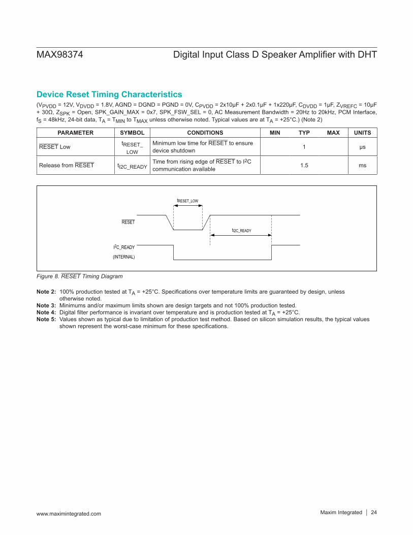
Figure 8. RESET Timing Diagram
Note 2: 100% production tested at TA = +25°C. Specifications over temperature limits are guaranteed by design, unless otherwise noted.
Note 3: Minimums and/or maximum limits shown are design targets and not 100% production tested.Note 4: Digital filter performance is invariant over temperature and is production tested at TA = +25°C.Note 5: Values shown as typical due to limitation of production test method. Based on silicon simulation results, the typical values
shown represent the worst-case minimum for these specifications.
Device Reset Timing Characteristics
RESET
I2C_READY
(INTERNAL)
tRESET_LOW
tI2C_READY
PARAMETER SYMBOL CONDITIONS MIN TYP MAX UNITS
RESET Low tRESET_ LOW
Minimum low time for RESET to ensure device shutdown 1 µs
Release from RESET tI2C_READYTime from rising edge of RESET to I2C communication available 1.5 ms
MAX98374 Digital Input Class D Speaker Amplifier with DHT
www.maximintegrated.com Maxim Integrated 24

(VPVDD = 12V, VDVDD = 1.8V, AGND = DGND = PGND = 0V, CPVDD = 2x10µF + 2x0.1µF+ 1x220µF, CDVDD = 1µF, ZVREFC = 10µF + 30Ω, ZSPK = Open, SPK_GAIN_MAX = 0x7, SPK_FSW_SEL = 0, AC Measurement Bandwidth = 20Hz to 20kHz, PCM Interface, fS = 48kHz, 24-bit data, TA = TMIN to TMAX. Typical values are at TA = +25°C.)
Typical Operating Characteristics
0
0.5
1.0
1.5
2.0
2.5
3.0
3.5
4.0
1.7 1.75 1.8 1.91.85
DVDD
QUIE
SCEN
TCU
RREN
T(m
A)
DVDD VOLTAGE (V)
DVDD QUIESCENT CURRENT vs.DVDD VOLTAGE
toc 01
ZSPK = ∞
0.0
0.1
0.2
0.3
0.4
0.5
0.6
0.7
0.8
0.9
1.0
5 6 7 8 9 10 11 12 13 14 15 16 17
PVDD
SOF
TWAR
E SH
UTDO
WN
CURR
ENT
(µA)
PVDD VOLTAGE (V)
ZSPK = ∞DAI PINS = GND
PVDD SOFTWARE SHUTDOWN CURRENT vs. PVDD VOLTAGE
toc 04
4.0
4.5
5.0
5.5
6.0
6.5
7.0
7.5
8.0
5 7 9 11 13 15 17
PVDD
QUIE
SCEN
TCU
RREN
T(m
A)
PVDD VOLTAGE (V)
ZSPK = ∞
fSPK_SW = 472kHz
fSPK_SW = 330kHz
PVDD QUIESCENT CURRENT vs.PVDD VOLTAGE
toc 02
0.00
0.01
0.02
0.03
0.04
0.05
0.06
0.07
0.08
0.09
0.10
1.70 1.75 1.80 1.85 1.90
DVDD
HAR
DWAR
E SH
UTDO
WN
CURR
ENT
(µA)
DVDD VOLTAGE (V)
ZSPK = ∞VRESET = GND
DVDD HARDWARE SHUTDOWN CURRENT vs. DVDD VOLTAGE
toc 05
0
2
4
6
8
10
12
14
16
18
20
1.70 1.75 1.80 1.85 1.90
DVDD
SOF
TWAR
E SH
UTDO
WN
CURR
ENT
(µA)
DVDD VOLTAGE (V)
ZSPK = ∞DAI PINS = GND
DVDD SOFTWARE SHUTDOWN CURRENT vs. DVDD VOLTAGE
toc 03
0.0
0.1
0.2
0.3
0.4
0.5
0.6
0.7
0.8
0.9
1.0
5 6 7 8 9 10 11 12 13 14 15 16 17
PVDD
HAR
DWAR
E SH
UTDO
WN
CURR
ENT
(µA)
PVDD VOLTAGE (V)
ZSPK = ∞VRESET = GND
PVDD HARDWARE SHUTDOWN CURRENT vs. PVDD VOLTAGE
toc 06
MAX98374 Digital Input Class D Speaker Amplifier with DHT
Maxim Integrated 25www.maximintegrated.com

(VPVDD = 12V, VDVDD = 1.8V, AGND = DGND = PGND = 0V, CPVDD = 2x10µF + 2x0.1µF+ 1x220µF, CDVDD = 1µF, ZVREFC = 10µF + 30Ω, ZSPK = Open, SPK_GAIN_MAX = 0x7, SPK_FSW_SEL = 0, AC Measurement Bandwidth = 20Hz to 20kHz, PCM Interface, fS = 48kHz, 24-bit data, TA = TMIN to TMAX. Typical values are at TA = +25°C.)
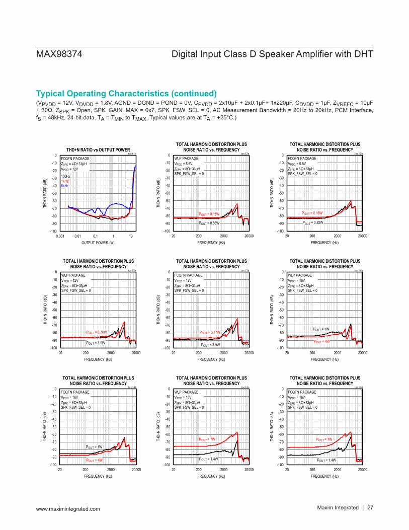
Typical Operating Characteristics (continued)
-100
-90
-80
-70
-60
-50
-40
-30
-20
-10
0
0.001 0.01 0.1 1 10
THD+
N RA
TIO (d
B)
OUTPUT POWER (W)
WLP PACKAGEZSPK = 8Ω+33µHVPDD = 5.5V
100Hz1kHz6kHz
THD+N RATIO vs OUTPUT POWERtoc 07a
-100
-90
-80
-70
-60
-50
-40
-30
-20
-10
0
0.001 0.01 0.1 1 10
THD+
N RA
TIO (d
B)
OUTPUT POWER (W)
FCQFN PACKAGEZSPK = 8Ω+33µHVPDD = 12V
100Hz1kHz6kHz
THD+N RATIO vs OUTPUT POWERtoc 08b
-100
-90
-80
-70
-60
-50
-40
-30
-20
-10
0
0.001 0.01 0.1 1 10
THD+
N RA
TIO (d
B)
OUTPUT POWER (W)
WLP PACKAGEZSPK = 4Ω+33µHVPDD = 5.5V
100Hz1kHz6kHz
THD+N RATIO vs OUTPUT POWERtoc 10a
-100
-90
-80
-70
-60
-50
-40
-30
-20
-10
0
0.001 0.01 0.1 1 10
THD+
N RA
TIO (d
B)
OUTPUT POWER (W)
FCQFN PACKAGEZSPK = 8Ω+33µHVPDD = 5.5V100Hz1kHz6kHz
THD+N RATIO vs OUTPUT POWERtoc 07b
-100
-90
-80
-70
-60
-50
-40
-30
-20
-10
0
0.001 0.01 0.1 1 10
THD+
N RA
TIO (d
B)
OUTPUT POWER (W)
WLP PACKAGEZSPK = 8Ω+33µHVPDD = 16V
100Hz1kHz6kHz
THD+N RATIO vs OUTPUT POWERtoc 09a
-100
-90
-80
-70
-60
-50
-40
-30
-20
-10
0
0.001 0.01 0.1 1 10
THD+
N RA
TIO (d
B)
OUTPUT POWER (W)
FCQFN PACKAGEZSPK = 4Ω+33µHVPDD = 5.5V100Hz1kHz6kHz
THD+N RATIO vs OUTPUT POWERtoc 10b
-100
-90
-80
-70
-60
-50
-40
-30
-20
-10
0
0.001 0.01 0.1 1 10
THD+
N RA
TIO (d
B)
OUTPUT POWER (W)
WLP PACKAGEZSPK = 8Ω+33µHVPDD = 12V
100Hz1kHz6kHz
THD+N RATIO vs OUTPUT POWERtoc 08a
-100
-90
-80
-70
-60
-50
-40
-30
-20
-10
0
0.001 0.01 0.1 1 10
THD+
N RA
TIO (d
B)
OUTPUT POWER (W)
FCQFN PACKAGEZSPK = 8Ω+33µHVPDD = 16V
100Hz1kHz6kHz
THD+N RATIO vs OUTPUT POWERtoc 09b
-100
-90
-80
-70
-60
-50
-40
-30
-20
-10
0
0.001 0.01 0.1 1 10
THD+
N RA
TIO (d
B)
OUTPUT POWER (W)
WLP PACKAGEZSPK = 4Ω+33µHVPDD = 12V
100Hz1kHz6kHz
THD+N RATIO vs OUTPUT POWERtoc 11a
MAX98374 Digital Input Class D Speaker Amplifier with DHT
Maxim Integrated 26www.maximintegrated.com
(VPVDD = 12V, VDVDD = 1.8V, AGND = DGND = PGND = 0V, CPVDD = 2x10µF + 2x0.1µF+ 1x220µF, CDVDD = 1µF, ZVREFC = 10µF + 30Ω, ZSPK = Open, SPK_GAIN_MAX = 0x7, SPK_FSW_SEL = 0, AC Measurement Bandwidth = 20Hz to 20kHz, PCM Interface, fS = 48kHz, 24-bit data, TA = TMIN to TMAX. Typical values are at TA = +25°C.)
Typical Operating Characteristics (continued)
-100
-90
-80
-70
-60
-50
-40
-30
-20
-10
0
0.001 0.01 0.1 1 10
THD+
N RA
TIO (d
B)
OUTPUT POWER (W)
FCQFN PACKAGEZSPK = 4Ω+33µHVPDD = 12V
100Hz1kHz6kHz
THD+N RATIO vs OUTPUT POWERtoc 11b
-100
-90
-80
-70
-60
-50
-40
-30
-20
-10
0
20 200 2000 20000
THD+
N RA
TIO (d
B)
FREQUENCY (Hz)
WLP PACKAGEVPDD = 12VZSPK = 8Ω+33µHSPK_FSW_SEL = 0
POUT = 3.9W
POUT = 0.78W
TOTAL HARMONIC DISTORTION PLUS NOISE RATIO vs. FREQUENCY
toc 13a
-100
-90
-80
-70
-60
-50
-40
-30
-20
-10
0
20 200 2000 20000
THD+
N RA
TIO (d
B)
FREQUENCY (Hz)
FCQFN PACKAGEVPDD = 16VZSPK = 8Ω+33µHSPK_FSW_SEL = 0
POUT = 1W
POUT = 4W
TOTAL HARMONIC DISTORTION PLUS NOISE RATIO vs. FREQUENCY
toc 14b
-100
-90
-80
-70
-60
-50
-40
-30
-20
-10
0
20 200 2000 20000
THD+
N RA
TIO (d
B)
FREQUENCY (Hz)
WLP PACKAGEVPDD = 5.5VZSPK = 8Ω+33µHSPK_FSW_SEL = 0
POUT = 0.83W
POUT = 0.16W
TOTAL HARMONIC DISTORTION PLUS NOISE RATIO vs. FREQUENCY
toc 12a
-100
-90
-80
-70
-60
-50
-40
-30
-20
-10
0
20 200 2000 20000
THD+
N RA
TIO (d
B)
FREQUENCY (Hz)
FCQFN PACKAGEVPDD = 12VZSPK = 8Ω+33µHSPK_FSW_SEL = 0
POUT = 3.9W
POUT = 0.77W
TOTAL HARMONIC DISTORTION PLUS NOISE RATIO vs. FREQUENCY
toc 13b
-100
-90
-80
-70
-60
-50
-40
-30
-20
-10
0
20 200 2000 20000
THD+
N RA
TIO (d
B)
FREQUENCY (Hz)
WLP PACKAGEVPDD = 16VZSPK = 8Ω+33µHSPK_FSW_SEL = 0
POUT = 1.4W
POUT = 7W
TOTAL HARMONIC DISTORTION PLUS NOISE RATIO vs. FREQUENCY
toc 14c
-100
-90
-80
-70
-60
-50
-40
-30
-20
-10
0
20 200 2000 20000
THD+
N RA
TIO (d
B)
FREQUENCY (Hz)
FCQFN PACKAGEVPDD = 5.5VZSPK = 8Ω+33µHSPK_FSW_SEL = 0
POUT = 0.82W
POUT = 0.16W
TOTAL HARMONIC DISTORTION PLUS NOISE RATIO vs. FREQUENCY
toc 12b
-100
-90
-80
-70
-60
-50
-40
-30
-20
-10
0
20 200 2000 20000
THD+
N RA
TIO (d
B)
FREQUENCY (Hz)
WLP PACKAGEVPDD = 16VZSPK = 8Ω+33µHSPK_FSW_SEL = 0
POUT = 1W
POUT = 4W
TOTAL HARMONIC DISTORTION PLUS NOISE RATIO vs. FREQUENCY
toc 14a
-100
-90
-80
-70
-60
-50
-40
-30
-20
-10
0
20 200 2000 20000
THD+
N RA
TIO (d
B)
FREQUENCY (Hz)
FCQFN PACKAGEVPDD = 16VZSPK = 8Ω+33µHSPK_FSW_SEL = 0
POUT = 1.4W
POUT = 7W
TOTAL HARMONIC DISTORTION PLUS NOISE RATIO vs. FREQUENCY
toc 14d
MAX98374 Digital Input Class D Speaker Amplifier with DHT
Maxim Integrated 27www.maximintegrated.com

(VPVDD = 12V, VDVDD = 1.8V, AGND = DGND = PGND = 0V, CPVDD = 2x10µF + 2x0.1µF+ 1x220µF, CDVDD = 1µF, ZVREFC = 10µF + 30Ω, ZSPK = Open, SPK_GAIN_MAX = 0x7, SPK_FSW_SEL = 0, AC Measurement Bandwidth = 20Hz to 20kHz, PCM Interface, fS = 48kHz, 24-bit data, TA = TMIN to TMAX. Typical values are at TA = +25°C.)
Typical Operating Characteristics (continued)
-100
-90
-80
-70
-60
-50
-40
-30
-20
-10
0
20 200 2000 20000
THD+
N RA
TIO (d
B)
FREQUENCY (Hz)
WLP PACKAGEVPDD = 5.5VZSPK = 4Ω+33µHSPK_FSW_SEL = 0
POUT = 0.1W
POUT = 1W
TOTAL HARMONIC DISTORTION PLUS NOISE RATIO vs. FREQUENCY
toc 15a
-100
-90
-80
-70
-60
-50
-40
-30
-20
-10
0
20 200 2000 20000
THD+
N RA
TIO (d
B)
FREQUENCY (Hz)
FCQFN PACKAGEVPDD = 12VZSPK = 4Ω+33µHSPK_FSW_SEL = 0
POUT = 6.3W
POUT = 1.26W
TOTAL HARMONIC DISTORTION PLUS NOISE RATIO vs. FREQUENCY
toc 16b
-100
-90
-80
-70
-60
-50
-40
-30
-20
-10
0
20 200 2000 20000
THD+
N RA
TIO (d
B)
FREQUENCY (Hz)
FCQFN PACKAGEVPDD = 5.5VZSPK = 4Ω+33µHSPK_FSW_SEL = 0
POUT = 0.1W
POUT = 1W
TOTAL HARMONIC DISTORTION PLUS NOISE RATIO vs. FREQUENCY
toc 15b
0.0
0.5
1.0
1.5
2.0
2.5
3.0
3.5
4.0
4.5
5.0
1 10 100
OUTP
UTPO
WER
(W)
LOAD RESISTANCE (RΩ)
VPVDD = 5.5VSPEAKER LOAD = RΩ+33µH
SPK_FSW_SEL = 0
1% THD+N
10% THD+N
OUTPUT POWER vs.LOAD RESISTANCE
toc17
-100
-90
-80
-70
-60
-50
-40
-30
-20
-10
0
20 200 2000 20000
THD+
N RA
TIO (d
B)
FREQUENCY (Hz)
WLP PACKAGEVPDD = 12VZSPK = 4Ω+33µHSPK_FSW_SEL = 0
POUT = 6.4W
POUT = 1.27W
TOTAL HARMONIC DISTORTION PLUS NOISE RATIO vs. FREQUENCY
toc 16a
MAX98374 Digital Input Class D Speaker Amplifier with DHT
Maxim Integrated 28www.maximintegrated.com
(VPVDD = 12V, VDVDD = 1.8V, AGND = DGND = PGND = 0V, CPVDD = 2x10µF + 2x0.1µF+ 1x220µF, CDVDD = 1µF, ZVREFC = 10µF + 30Ω, ZSPK = Open, SPK_GAIN_MAX = 0x7, SPK_FSW_SEL = 0, AC Measurement Bandwidth = 20Hz to 20kHz, PCM Interface, fS = 48kHz, 24-bit data, TA = TMIN to TMAX. Typical values are at TA = +25°C.)
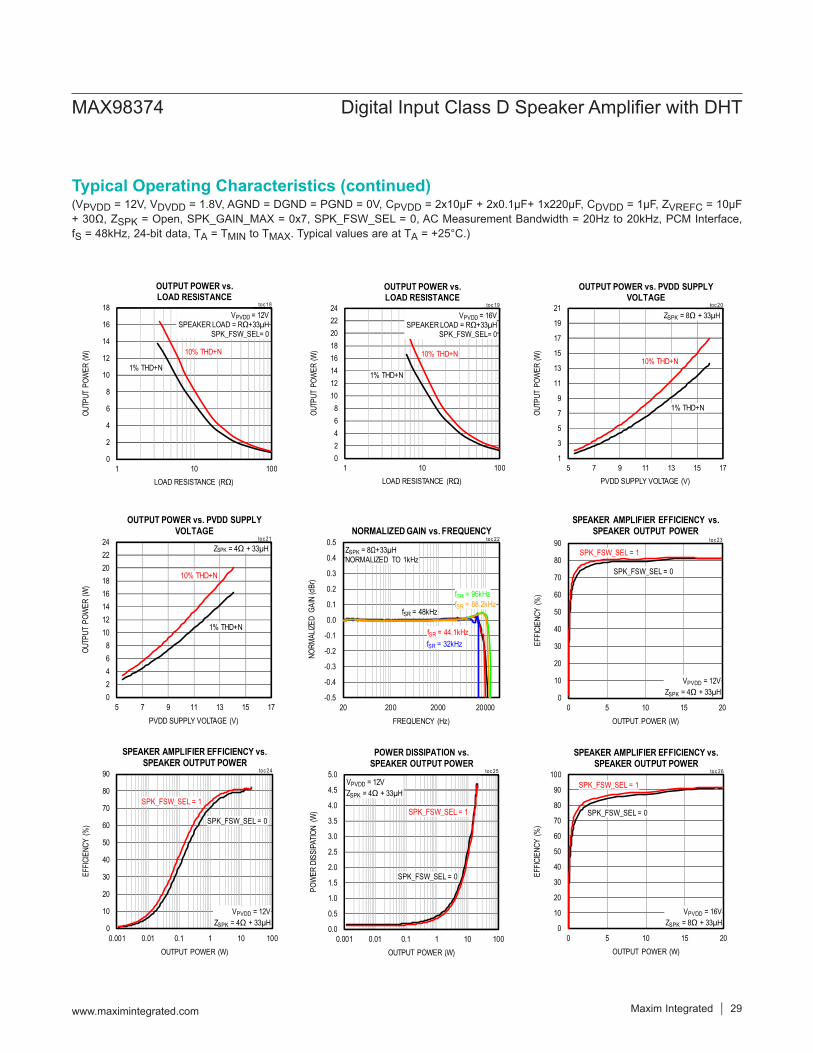
Typical Operating Characteristics (continued)
0
2
4
6
8
10
12
14
16
18
1 10 100
OUTP
UTPO
WER
(W)
LOAD RESISTANCE (RΩ)
VPVDD = 12VSPEAKER LOAD = RΩ+33µH
SPK_FSW_SEL= 0
1% THD+N
10% THD+N
OUTPUT POWER vs.LOAD RESISTANCE
toc 18
02468
1012141618202224
5 7 9 11 13 15 17
OUTP
UTPO
WER
(W)
PVDD SUPPLY VOLTAGE (V)
ZSPK = 4Ω + 33µH
1% THD+N
10% THD+N
OUTPUT POWER vs. PVDD SUPPLYVOLTAGE
toc 21
0
10
20
30
40
50
60
70
80
90
0.001 0.01 0.1 1 10 100
EFFIC
IENC
Y (%
)
OUTPUT POWER (W)
VPVDD = 12VZSPK = 4Ω + 33µH
SPK_FSW_SEL = 0
SPK_FSW_SEL = 1
SPEAKER AMPLIFIER EFFICIENCY vs. SPEAKER OUTPUT POWER
toc 24
02468
1012141618202224
1 10 100
OUTP
UTPO
WER
(W)
LOAD RESISTANCE (RΩ)
VPVDD = 16VSPEAKER LOAD = RΩ+33µH
SPK_FSW_SEL= 0
1% THD+N
10% THD+N
OUTPUT POWER vs.LOAD RESISTANCE
toc 19
-0.5
-0.4
-0.3
-0.2
-0.1
0.0
0.1
0.2
0.3
0.4
0.5
20 200 2000 20000
NORM
ALIZE
D GA
IN (d
Br)
FREQUENCY (Hz)
ZSPK = 8Ω+33µHNORMALIZED TO 1kHz
fSR = 48kHz
fSR = 44.1kHzfSR = 32kHz
fSR = 96kHzfSR = 88.2kHz
NORMALIZED GAIN vs. FREQUENCYtoc 22
0.0
0.5
1.0
1.5
2.0
2.5
3.0
3.5
4.0
4.5
5.0
0.001 0.01 0.1 1 10 100
POW
ERDI
SSIPA
TION
(W)
OUTPUT POWER (W)
VPVDD = 12VZSPK = 4Ω + 33µH
SPK_FSW_SEL = 0
SPK_FSW_SEL = 1
POWER DISSIPATION vs.SPEAKER OUTPUT POWER
toc 25
1
3
5
7
9
11
13
15
17
19
21
5 7 9 11 13 15 17
OUTP
UTPO
WER
(W)
PVDD SUPPLY VOLTAGE (V)
ZSPK = 8Ω + 33µH
1% THD+N
10% THD+N
OUTPUT POWER vs. PVDD SUPPLYVOLTAGE
toc 20
0
10
20
30
40
50
60
70
80
90
0 5 10 15 20
EFFIC
IENC
Y (%
)
OUTPUT POWER (W)
SPEAKER AMPLIFIER EFFICIENCY vs. SPEAKER OUTPUT POWER
VPVDD = 12VZSPK = 4Ω + 33µH
SPK_FSW_SEL = 0
SPK_FSW_SEL = 1toc 23
0
10
20
30
40
50
60
70
80
90
100
0 5 10 15 20
EFFIC
IENC
Y (%
)
OUTPUT POWER (W)
VPVDD = 16VZSPK = 8Ω + 33µH
SPK_FSW_SEL = 0
SPK_FSW_SEL = 1
SPEAKER AMPLIFIER EFFICIENCY vs. SPEAKER OUTPUT POWER
toc 26
MAX98374 Digital Input Class D Speaker Amplifier with DHT
Maxim Integrated 29www.maximintegrated.com

(VPVDD = 12V, VDVDD = 1.8V, AGND = DGND = PGND = 0V, CPVDD = 2x10µF + 2x0.1µF+ 1x220µF, CDVDD = 1µF, ZVREFC = 10µF + 30Ω, ZSPK = Open, SPK_GAIN_MAX = 0x7, SPK_FSW_SEL = 0, AC Measurement Bandwidth = 20Hz to 20kHz, PCM Interface, fS = 48kHz, 24-bit data, TA = TMIN to TMAX. Typical values are at TA = +25°C.)
Typical Operating Characteristics (continued)
0
10
20
30
40
50
60
70
80
90
100
0.001 0.01 0.1 1 10 100
EFFIC
IENC
Y (%
)
OUTPUT POWER (W)
VPVDD = 16VZSPK = 8Ω + 33µH
SPK_FSW_SEL = 0
SPK_FSW_SEL = 1
SPEAKER AMPLIFIER EFFICIENCY vs. SPEAKER OUTPUT POWER
toc 27
0
10
20
30
40
50
60
70
80
90
100
0.001 0.01 0.1 1 10 100
EFFIC
IENC
Y(%
)
OUTPUT POWER (W)
VPVDD = 12VZSPK = 8Ω + 33µH
SPK_FSW_SEL = 0
SPK_FSW_SEL = 1
SPEAKER AMPLIFIER EFFICIENCY vs.SPEAKER OUTPUT POWER
toc 30
0
20
40
60
80
100
120
5 7 9 11 13 15 17
PSRR
(dB)
PVDD SUPPLY LEVEL (V)
fS = 1kHzVRIPPLE = 100mVP-PZSPK = ∞
PVDD POWER-SUPPLY REJECTION RATIO vs PVDD POWER SUPPLY
LEVELtoc 33
0.0
0.5
1.0
1.5
2.0
2.5
0.001 0.01 0.1 1 10 100
POW
ERDI
SSIPA
TION
(W)
OUTPUT POWER (W)
VPVDD = 16VZSPK = 8Ω + 33µH
SPK_FSW_SEL = 0
SPK_FSW_SEL = 1
POWER DISSIPATION vs.SPEAKER OUTPUT POWER
toc 28
0.0
0.2
0.4
0.6
0.8
1.0
1.2
1.4
0.001 0.01 0.1 1 10 100
EFFIC
IENC
Y (%
)
OUTPUT POWER (W)
VPVDD = 12VZSPK = 8Ω + 33µH
SPK_FSW_SEL = 0
SPK_FSW_SEL = 1
POWER DISSIPATION vs.SPEAKER OUTPUT POWER
toc 31
0
20
40
60
80
100
120
0.01 0.1 1 10 100
PSRR
(dB)
FREQUENCY (kHz)
VRIPPLE = 50mVP-PZSPK = ∞
DVDD POWER-SUPPLY REJECTION RATIO vs. FREQUENCY
toc 34
0
10
20
30
40
50
60
70
80
90
100
0 5 10 15
EFFIC
IENC
Y (%
)
OUTPUT POWER (W)
VPVDD = 12VZSPK = 8Ω + 33µH
SPK_FSW_SEL = 0
SPK_FSW_SEL = 1
SPEAKER AMPLIFIER EFFICIENCY vs. SPEAKER OUTPUT POWER
toc 29
0
20
40
60
80
100
120
0.01 0.1 1 10 100
PSRR
(dB)
FREQUENCY (kHz)
VPVDD = 12VVRIPPLE = 100mVPP
PVDD POWER-SUPPLY REJECTION RATIO vs. FREQUENCY
toc 32
0
20
40
60
80
100
120
1.70 1.75 1.80 1.85 1.90
PSRR
(dB)
DVDD SUPPLY LEVEL (V)
fS = 1kHzVRIPPLE = 50mVP-P
DVDD POWER-SUPPLY REJECTIONRATIO vs. DVDD POWER SUPPLY
LEVELtoc 35
MAX98374 Digital Input Class D Speaker Amplifier with DHT
Maxim Integrated 30www.maximintegrated.com

(VPVDD = 12V, VDVDD = 1.8V, AGND = DGND = PGND = 0V, CPVDD = 2x10µF + 2x0.1µF+ 1x220µF, CDVDD = 1µF, ZVREFC = 10µF + 30Ω, ZSPK = Open, SPK_GAIN_MAX = 0x7, SPK_FSW_SEL = 0, AC Measurement Bandwidth = 20Hz to 20kHz, PCM Interface, fS = 48kHz, 24-bit data, TA = TMIN to TMAX. Typical values are at TA = +25°C.)
Typical Operating Characteristics (continued)
SCL1V/div
SPKOUT2V/div
2ms/div
SOFTWARE ENABLETURN-ON RESPONSE
VOLUME RAMPING ENABLEDtoc 36
SCL1V/div
SPKOUT2V/div
800µs/div
SOFTWARE DISABLETURN-OFF RESPONSE
VOLUME RAMPING DISABLEDtoc 39
SCL1V/div
SPKOUT2V/div
800µs/div
SOFTWARE ENABLETURN-ON RESPONSE
VOLUME RAMPING DISABLEDtoc 37
RESET1V/div
SPKOUT2V/div
800µs/div
HARDWARE RESETTURN-OFF RESPONSE
toc 40
SCL1V/div
SPKOUT2V/div
2ms/div
SOFTWARE DISABLETURN-OFF RESPONSE
VOLUME RAMPING ENABLEDtoc 38
BCLK1V/div
LRCLK2V/div
FILTEREDCLASS D2V/div
200µs/div
BCLK REMOVALTURN-OFF RESPONSE
toc 41
MAX98374 Digital Input Class D Speaker Amplifier with DHT
Maxim Integrated 31www.maximintegrated.com

(VPVDD = 12V, VDVDD = 1.8V, AGND = DGND = PGND = 0V, CPVDD = 2x10µF + 2x0.1µF+ 1x220µF, CDVDD = 1µF, ZVREFC = 10µF + 30Ω, ZSPK = Open, SPK_GAIN_MAX = 0x7, SPK_FSW_SEL = 0, AC Measurement Bandwidth = 20Hz to 20kHz, PCM Interface, fS = 48kHz, 24-bit data, TA = TMIN to TMAX. Typical values are at TA = +25°C.)
Typical Operating Characteristics (continued)
-140
-120
-100
-80
-60
-40
-20
0
20
40
0 5000 10000 15000
AMPL
ITUDE
(dBV
)
FREQUENCY (Hz)
WLP PACKAGEZSPK = 8Ω+33µH
fSR = 32kHzLARGE SIGNAL, 1kHz SINEWAVE INPUT
INBAND OUTPUT SPECTRUMtoc 42a
-140
-120
-100
-80
-60
-40
-20
0
20
40
0 5000 10000 15000
AMPL
ITUDE
(dBV
)
FREQUENCY (Hz)
FCQFN PACKAGEZSPK = 8Ω+33µH
fSR = 32kHz1kHz SINEWAVE INPUT
INBAND OUTPUT SPECTRUMtoc 42b
-140
-120
-100
-80
-60
-40
-20
0
20
40
0 5000 10000 15000 20000
AMPL
ITUDE
(dBV
)
FREQUENCY (Hz)
WLP PACKAGEZSPK = 8Ω+33µH
fSR = 44.1kHz1kHz SINEWAVE INPUT
INBAND OUTPUT SPECTRUMtoc 45a
-140
-120
-100
-80
-60
-40
-20
0
20
40
0 5000 10000 15000
AMPL
ITUDE
(dBV
)
FREQUENCY (Hz)
WLP PACKAGEZSPK = 8Ω+33µH
fSR = 32kHzSMALL SIGNAL, 1kHz SINEWAVE INPUT
INBAND OUTPUT SPECTRUMtoc 43a
-140
-120
-100
-80
-60
-40
-20
0
20
40
0 5000 10000 15000
AMPL
ITUDE
(dBV
)
FREQUENCY (Hz)
FCQFN PACKAGEZSPK = 8Ω+33µH
fSR = 32kHz1kHz SINEWAVE INPUT
INBAND OUTPUT SPECTRUMtoc 43b
-140
-120
-100
-80
-60
-40
-20
0
20
40
0 5000 10000 15000 20000
AMPL
ITUDE
(dBV
)
FREQUENCY (Hz)
WLP PACKAGEZSPK = 8Ω+33µH
fSR = 44.1kHz1kHz SINEWAVE INPUT
INBAND OUTPUT SPECTRUMtoc 46a
-140
-120
-100
-80
-60
-40
-20
0
20
40
0 5000 10000 15000
AMPL
ITUDE
(dBV
)
FREQUENCY (Hz)
WLP PACKAGEZSPK = 8Ω+33µH
fSR = 32kHzIDLE INPUT
INBAND OUTPUT SPECTRUMtoc 44a
-140
-120
-100
-80
-60
-40
-20
0
20
40
0 5000 10000 15000
AMPL
ITUDE
(dBV
)
FREQUENCY (Hz)
FCQFN PACKAGEZSPK = 8Ω+33µH
fSR = 32kHz
INBAND OUTPUT SPECTRUMtoc 44b
-140
-120
-100
-80
-60
-40
-20
0
20
40
0 5000 10000 15000 20000
AMPL
ITUDE
(dBV
)
FREQUENCY (Hz)
WLP PACKAGEZSPK = 8Ω+33µH
fSR = 44.1kHz
INBAND OUTPUT SPECTRUMtoc 47a
MAX98374 Digital Input Class D Speaker Amplifier with DHT
Maxim Integrated 32www.maximintegrated.com

(VPVDD = 12V, VDVDD = 1.8V, AGND = DGND = PGND = 0V, CPVDD = 2x10µF + 2x0.1µF+ 1x220µF, CDVDD = 1µF, ZVREFC = 10µF + 30Ω, ZSPK = Open, SPK_GAIN_MAX = 0x7, SPK_FSW_SEL = 0, AC Measurement Bandwidth = 20Hz to 20kHz, PCM Interface, fS = 48kHz, 24-bit data, TA = TMIN to TMAX. Typical values are at TA = +25°C.)
Typical Operating Characteristics (continued)
-140
-120
-100
-80
-60
-40
-20
0
20
40
0 5000 10000 15000 20000
AMPL
ITUDE
(dBV
)
FREQUENCY (Hz)
FCQFN PACKAGEZSPK = 8Ω+33µH
fSR = 44.1kHz1kHz SINEWAVE INPUT
INBAND OUTPUT SPECTRUMtoc 45b
-140
-120
-100
-80
-60
-40
-20
0
20
40
0 5000 10000 15000 20000
AMPL
ITUDE
(dBV
)
FREQUENCY (Hz)
WLP PACKAGEZSPK = 8Ω+33µH
fSR = 48kHz1kHz SINEWAVE INPUT
INBAND OUTPUT SPECTRUMtoc 48a
-140
-120
-100
-80
-60
-40
-20
0
20
40
0 5000 10000 15000 20000
AMPL
ITUDE
(dBV
)
FREQUENCY (Hz)
FCQFN PACKAGEZSPK = 8Ω+33µH
fSR = 48kHz1kHz SINEWAVE INPUT
INBAND OUTPUT SPECTRUMtoc 48b
-140
-120
-100
-80
-60
-40
-20
0
20
40
0 5000 10000 15000 20000
AMPL
ITUDE
(dBV
)
FREQUENCY (Hz)
FCQFN PACKAGEZSPK = 8Ω+33µH
fSR = 44.1kHz1kHz SINEWAVE INPUT
INBAND OUTPUT SPECTRUMtoc 46b
-140
-120
-100
-80
-60
-40
-20
0
20
40
0 5000 10000 15000 20000
AMPL
ITUDE
(dBV
)
FREQUENCY (Hz)
WLP PACKAGEZSPK = 8Ω+33µH
fSR = 48kHz1kHz SINEWAVE INPUT
INBAND OUTPUT SPECTRUMtoc 49a
-140
-120
-100
-80
-60
-40
-20
0
20
40
0 5000 10000 15000 20000
AMPL
ITUDE
(dBV
)
FREQUENCY (Hz)
FCQFN PACKAGEZSPK = 8Ω+33µH
fSR = 48kHz1kHz SINEWAVE INPUT
INBAND OUTPUT SPECTRUMtoc 49b
-140
-120
-100
-80
-60
-40
-20
0
20
40
0 5000 10000 15000 20000
AMPL
ITUDE
(dBV
)
FREQUENCY (Hz)
FCQFN PACKAGEZSPK = 8Ω+33µH
fSR = 44.1kHz
INBAND OUTPUT SPECTRUMtoc 47b
-140
-120
-100
-80
-60
-40
-20
0
20
40
0 5000 10000 15000 20000
AMPL
ITUDE
(dBV
)
FREQUENCY (Hz)
WLP PACKAGEZSPK = 8Ω+33µH
fSR = 48kHz
INBAND OUTPUT SPECTRUMtoc 50a
-140
-120
-100
-80
-60
-40
-20
0
20
40
0 5000 10000 15000 20000
AMPL
ITUDE
(dBV
)
FREQUENCY (Hz)
FCQFN PACKAGEZSPK = 8Ω+33µH
fSR = 48kHz
INBAND OUTPUT SPECTRUMtoc 50b
MAX98374 Digital Input Class D Speaker Amplifier with DHT
Maxim Integrated 33www.maximintegrated.com

(VPVDD = 12V, VDVDD = 1.8V, AGND = DGND = PGND = 0V, CPVDD = 2x10µF + 2x0.1µF+ 1x220µF, CDVDD = 1µF, ZVREFC = 10µF + 30Ω, ZSPK = Open, SPK_GAIN_MAX = 0x7, SPK_FSW_SEL = 0, AC Measurement Bandwidth = 20Hz to 20kHz, PCM Interface, fS = 48kHz, 24-bit data, TA = TMIN to TMAX. Typical values are at TA = +25°C.)
Typical Operating Characteristics (continued)
-140
-120
-100
-80
-60
-40
-20
0
20
40
0 5000 10000 15000 20000
AMPL
ITUDE
(dBV
)
FREQUENCY (Hz)
WLP PACKAGEZSPK = 8Ω+33µH
fSR = 88.2kHz1kHz SINEWAVE INPUT
INBAND OUTPUT SPECTRUMtoc 51a
-140
-120
-100
-80
-60
-40
-20
0
20
40
0 5000 10000 15000 20000
AMPL
ITUDE
(dBV
)
FREQUENCY (Hz)
FCQFN PACKAGEZSPK = 8Ω+33µH
fSR = 88.2kHz1kHz SINEWAVE INPUT
INBAND OUTPUT SPECTRUMtoc 51b
-140
-120
-100
-80
-60
-40
-20
0
20
40
0 5000 10000 15000 20000
AMPL
ITUDE
(dBV
)
FREQUENCY (Hz)
WLP PACKAGEZSPK = 8Ω+33µH
fSR = 96kHz1kHz SINEWAVE INPUT
INBAND OUTPUT SPECTRUMtoc 54a
-140
-120
-100
-80
-60
-40
-20
0
20
40
0 5000 10000 15000 20000
AMPL
ITUDE
(dBV
)
FREQUENCY (Hz)
WLP PACKAGEZSPK = 8Ω+33µH
fSR = 88.2kHz1kHz SINEWAVE INPUT
INBAND OUTPUT SPECTRUMtoc 52a
-140
-120
-100
-80
-60
-40
-20
0
20
40
0 5000 10000 15000 20000
AMPL
ITUDE
(dBV
)
FREQUENCY (Hz)
FCQFN PACKAGEZSPK = 8Ω+33µH
fSR = 88.2kHz1kHz SINEWAVE INPUT
INBAND OUTPUT SPECTRUMtoc 52b
-140
-120
-100
-80
-60
-40
-20
0
20
40
0 5000 10000 15000 20000
AMPL
ITUDE
(dBV
)
FREQUENCY (Hz)
WLP PACKAGEZSPK = 8Ω+33µH
fSR = 96kHz1kHz SINEWAVE INPUT
INBAND OUTPUT SPECTRUMtoc 55a
-140
-120
-100
-80
-60
-40
-20
0
20
40
0 5000 10000 15000 20000
AMPL
ITUDE
(dBV
)
FREQUENCY (Hz)
WLP PACKAGEZSPK = 8Ω+33µH
fSR = 88.2kHz
INBAND OUTPUT SPECTRUMtoc 53a
-140
-120
-100
-80
-60
-40
-20
0
20
40
0 5000 10000 15000 20000
AMPL
ITUDE
(dBV
)
FREQUENCY (Hz)
FCQFN PACKAGEZSPK = 8Ω+33µH
fSR = 88.2kHz
INBAND OUTPUT SPECTRUMtoc 53b
-140
-120
-100
-80
-60
-40
-20
0
20
40
0 5000 10000 15000 20000
AMPL
ITUDE
(dBV
)
FREQUENCY (Hz)
WLP PACKAGEZSPK = 8Ω+33µH
fSR = 96kHz
INBAND OUTPUT SPECTRUMtoc 56a
MAX98374 Digital Input Class D Speaker Amplifier with DHT
Maxim Integrated 34www.maximintegrated.com

(VPVDD = 12V, VDVDD = 1.8V, AGND = DGND = PGND = 0V, CPVDD = 2x10µF + 2x0.1µF+ 1x220µF, CDVDD = 1µF, ZVREFC = 10µF + 30Ω, ZSPK = Open, SPK_GAIN_MAX = 0x7, SPK_FSW_SEL = 0, AC Measurement Bandwidth = 20Hz to 20kHz, PCM Interface, fS = 48kHz, 24-bit data, TA = TMIN to TMAX. Typical values are at TA = +25°C.)
Typical Operating Characteristics (continued)
-140
-120
-100
-80
-60
-40
-20
0
20
40
0 5000 10000 15000 20000
AMPL
ITUDE
(dBV
)
FREQUENCY (Hz)
FCQFN PACKAGEZSPK = 8Ω+33µH
fSR = 96kHz1kHz SINEWAVE INPUT
INBAND OUTPUT SPECTRUMtoc 54b
FILTEREDCLASS D12.5V/div
FOUTP10V/div
FOUTN10V/div
200µs/div
CLIPPING RESPONSE FOR 1% THD+ND Ntoc 57
-100
-80
-60
-40
-20
0
20
0 200 400 600 800 1000
AMPL
ITUDE
(dBV
)
FREQUENCY (kHz)
SSM_MOD_INDEX = 0x05 (MMI*1/6)
CLASS D OUTPUT FFT vs.FREQUENCY
toc60
-140
-120
-100
-80
-60
-40
-20
0
20
40
0 5000 10000 15000 20000
AMPL
ITUDE
(dBV
)
FREQUENCY (Hz)
FCQFN PACKAGEZSPK = 8Ω+33µH
fSR = 96kHz1kHz SINEWAVE INPUT
INBAND OUTPUT SPECTRUMtoc 55b
FILTEREDCLASS D12.5V/div
FOUTP10V/div
FOUTN10V/div
200µs/div
CLIPPING RESPONSE FOR 10%THD+N
toc 58
-1.0
-0.8
-0.6
-0.4
-0.2
0.0
0.2
0.4
0.6
0.8
1.0
0 5000 10000 15000 20000
NORM
ALIZE
DOU
TPUT
AMPL
ITUDE
(dBr
)
FREQUENCY (Hz)
NORMALIZED TO 1kHz,OUTPUT RELATIVE TO 1% THD+N
-3dBrG-10dBrG-20dBrG
NORMALIZED SPEAKER OUTPUTRESPONSE vs. FREQUENCY
toc 61
-140
-120
-100
-80
-60
-40
-20
0
20
40
0 5000 10000 15000 20000
AMPL
ITUDE
(dBV
)
FREQUENCY (Hz)
FCQFN PACKAGEZSPK = 8Ω+33µH
fSR = 96kHz
INBAND OUTPUT SPECTRUMtoc 56b
-100
-80
-60
-40
-20
0
20
0 200 400 600 800 1000
AMPL
ITUDE
( dBV
)
FREQUENCY (kHz)
SSM OFF
CLASS D OUTPUT FFT vs.FREQUENCY
toc 59
-35
-30
-25
-20
-15
-10
-5
0
5
0.1 1 10 100
NORM
ALIZE
DAM
PLITU
DE(d
BFS)
FREQUENCY (Hz)
48kHz96kHz
16kHz
CLASS D DC BLOCKER CORNERFREQUENCY
toc 62
MAX98374 Digital Input Class D Speaker Amplifier with DHT
Maxim Integrated 35www.maximintegrated.com

Pin Configuration (WLP)
OUTN
I.C.
SDAOUTNSNS
ICCADDRVREFC
PGND PGND SCLAGND
OUTN
1 2 3 4
+
C
D
E
MAX98374
WLP(2.17mm x 2.25mm x 0.64mm, 0.4mm Pitch)
TOP VIEW(BUMP SIDE DOWN)
A
B
5
DIN/SWDATA
DGND
DOUT
OUTP LRCLKOUTPSNSOUTP BCLK/SWCLK
PVDD DVDDIRQPVDD RESET
ANALOG
HIGH POWER
DIGITAL
MAX98374 Digital Input Class D Speaker Amplifier with DHT
www.maximintegrated.com Maxim Integrated 36

Pin Configuration (FCQFN)
22 21
MAX98374
FCQFN(3mm x 3mm x 0.55mm, 0.4mm Pitch)
TOP VIEWO
UTN
SNS
VREF
C
AG
ND
I.C.
AD
DR
SCL
SDA
ICC
DOUT
DIN / SWDATA
BCLK / SWCLK
LRC
LK
RES
ET
DG
ND
DVD
D
OUTPSNS
PVDD
OUTP
OUTN
PGND
IRQ
DIGITAL ANALOG HIGH POWER
20 19 18
116 7 8 9 10
17
5
4
3
2
1 16
12
13
14
15
PVD
D
MAX98374 Digital Input Class D Speaker Amplifier with DHT
www.maximintegrated.com Maxim Integrated 37

Pin Description
WLP FCQFN NAME SUPPLY RAIL FUNCTION
A1, A2 11, 12 PVDD —Speaker Amplifier Power Supply. Bypass each bump to PGND with a 0.1µF and 10µF capacitor (two of each total) placed as close as possible. Bypass the supply bus to PGND with a single 220µF bulk capacitor per device.
A3 10 IRQ DVDD Hardware Interrupt Output. Interrupt polarity and pin drive mode are configurable. Connect a 1.5kΩ pullup resistor to DVDD for full logic level swing in open-drain mode.
A4 9 DVDD — Digital Power Supply. Power supply for the digital core and digital interface pins. Bypass to DGND with 1µF capacitor.
A5 6 RESET DVDDActive-Low Hardware Reset. Resets all digital portions of the device and all registers to default PoR settings. DVDD must be in the valid operating range before driving high. Do not connect directly to DVDD.
B1, B2 13 OUTP PVDD Positive Speaker Amplifier Output
B3 16 OUTPSNS PVDD Speaker Amplifier Feedback Positive Input. Connect as close as possible to the positive terminal of the loudspeaker. This pin must form a complete loop with OUTP.
B4 7 LRCLK DVDD PCM Interface Frame Clock Input. LRCLK frequency matches the PCM interface sample rate. Internally pulled down to DGND through RPD.
B5 5 BCLK/ SWCLK DVDD PCM Interface Bit Clock Input/SoundWire Compatible Interface Clock Input.
Internally pulled down to DGND through RPD.
C1, C2 14 OUTN PVDD Negative Speaker Amplifier Output
C3 17 OUTNSNS PVDDSpeaker Amplifier Feedback Negative Input. Connect as close as possible to the negative terminal of the loudspeaker. This pin must form a complete loop with OUTN.
C4 1 SDA DVDD I2C-Compatible Serial-Data. Connect a 1.5kΩ pullup resistor to DVDD for full logic level swing. In SoundWire control mode, connect to either DVDD or DGND.
C5 4 DIN/ SWDATA DVDD PCM Interface Data Input/SoundWire Compatible Interface Data Bus. Internally
pulled down to DGND through RIN.
D1, D2 15 PGND — Speaker Amplifier Ground
D3 19 AGND — Analog Ground. Connecting AGND to PGND on the top layer of the PCB is not recommended.
D4 22 SCL DVDD I2C-Compatible Serial-Clock. Connect a 1.5kΩ pullup resistor to DVDD for full logic level swing. In SoundWire control mode, connect to either DVDD or DGND.
D5 3 DOUT DVDD PCM Interface Data Output
E1 20 I.C. DVDD Internally Connected. Connect to DVDD externally. Do not connect to ground or leave unconnected.
E2 18 VREFC PVDD Internal Bias. Bypass to AGND with a 30Ω resistor and a 10µF capacitor.
E3 21 ADDR DVDD I2C Slave Address Select. Selects one of four I2C slave addresses.
E4 2 ICC DVDDInterchip Communication Data Bus. Optionally allows multiple devices to be grouped up to communicate with each other in order to provide a consistent response. Internally pulled down to DGND by RPD.
E5 8 DGND — Digital Ground
MAX98374 Digital Input Class D Speaker Amplifier with DHT
www.maximintegrated.com Maxim Integrated 38

Detailed DescriptionControl Interface ConfigurationThe device features a SoundWire compatible slave inter-face, an I2C slave interface, and a PCM audio interface (Figure 9). After initially powering up both supplies or when exiting hardware shutdown, the device control mode defaults to the SoundWire compatible interface. In this control mode, the SoundWire Compatible inter-face is used to program all device registers and for all digital audio data communication. In SoundWire control mode, the device I2C interface bus connections cannot be shared with another device, and the ADDR, SDA, and
SCL pins must each be connected to either DVDD or DGND to configure the SoundWire ID (Table 14).Any time after initial power-up, if the device is not in hard-ware shutdown and an I2C start condition is detected, the device automatically switches to I2C control mode. The I2C start condition that causes the switch over can be part of a normal I2C transaction. In I2C control mode, the I2C interface is used to program the general control registers while the PCM interface is used for all digital audio data communication. Once the device is in I2C control mode, only a full supply power cycle or hardware shutdown event can return the device to SoundWire control mode.
Figure 9. Control Interface Configuration Options
I2C CONTROL BUS
SOUNDWIRE BUS
SOUNDWIRE COMPATIBLE INTERFACE
CONTROL AND AUDIO MODE
PCM BUS
I2C INTERFACE CONTROL MODE
+ PCM AUDIO
MODE
IRQ TO MASTER
MAX98374MAX98374
AUDIO / DATA PATHS
SOUNDWIRE AND GENERAL
CONTROL REGISTERS
IRQ OUTPUT
SOUNDWIRE SLAVE
INTERFACE
SOUNDWIRE CONTROL
REGISTERS(INACCESSIBLE)
GENERAL CONTROL
REGISTERS
PCM INTERFACE
AUDIO / DATA PATHS
I2C INTERFACE
IRQ OUTPUT
MAX98374 Digital Input Class D Speaker Amplifier with DHT
www.maximintegrated.com Maxim Integrated 39

Device Register MapThe general control registers in the address space 0x2000 and above are accessible through both the SoundWire compatible and I2C interface and are used for configuring the device (except the SoundWire com-patible interface). The registers in the address space 0x0040 to 0x0337 are only accessible through the SoundWire compatible interface and are used for config-uring the SoundWire slave interface settings (Figure 9). Register bit fields come in several varieties that are sum-marized and color coded in Table 1.Read-only bit fields (R) are used to indicate an internal device state and cannot be changed directly by the host. Writing to these registers has no effect. Read-only status
bit fields are the same, however, writing a 1 to these registers clears the status while writing a 0 has no effect.Write-only bit fields (W) are single-bit push-button con-trols. Writing a 1 to these bit fields performs an action (i.e., software reset, interrupt clear, etc.). Writing a 0 has no effect and readback always returns a 0.Read/write bit fields (RW) can be both read and written by the host, and the last written value is the value returned on read back.Reserved bit fields (indicated by a “—“ in Table 2) are not used to program or control the device. When writing a register that contains reserved bit fields, always write a 0 to the reserved bit field segments.
Table 1. Register Map Bit Field Color CodingBIT FIELD TYPE FUNCTIONAL DESCRIPTION
Read-Only Bit Field A write to a read-only bit field has no effect.
Read-Only Status Bit Field (Clear on Write)
Write a 1 to clear a read-only status bit field.A write of 0 has no effect.
Write-Only Bit Field Write a 1 to activate the function of a write-only bit field.A write of 0 has no effect, and readback always returns 0.
Read/Write Bit Field Read and write commands function normally.There can be write access restrictions.
Reserved Bit Field Always write a 0 to a reserved bit field.
MAX98374 Digital Input Class D Speaker Amplifier with DHT
www.maximintegrated.com Maxim Integrated 40

Table 2. General Control Register MapREGISTER PROPERTIES REGISTER CONTENTS
ADDR POR REGISTER NAME BIT 7 BIT 6 BIT 5 BIT 4 BIT 3 BIT 2 BIT 1 BIT 0
SOFTWARE RESET REGISTER0x2000 0x00 Software Reset — — — — — — — RST
INTERRUPT REGISTERS
0x2001 0x00 Interrupt Raw 1
THERMSHDN_ BGN_RAW
THERMSHDN_END_RAW
THERMWARN_BGN_RAW
THERMWARN_END_RAW
BDE_L4_ RAW
BDE_LEVEL_ RAW
BDE_ACTIVE_ BGN_RAW
BDE_ACTIVE_ END_RAW
0x2002 0x00 Interrupt Raw 2
PWRUP_ DONE_RAW
PWRDN_ DONE_RAW
OTP_FAIL_ RAW
SPK_OVC_ RAW
CLKSTART_ RAW
CLKSTOP_ RAW
ICC_SYNC_ ERR_RAW
ICC_DATA_ ERR_RAW
0x2003 0x00 Interrupt Raw 3
PVDD_UVLO_ SHDN_RAW — THERMFB_
BGN_RAWTHERMFB_ END_RAW
DHT_ACTIVE _BGN_RAW
DHT_ACTIVE_ END_RAW
LMTR_ACTIVE _BGN_RAW
LMTR_ACTIVE _END_RAW
0x2004 0x00 Interrupt State 1
THERMSHDN_ BGN_STATE
THERMSHDN_ END_STATE
THERMWARN _BGN_STATE
THERMWARN _END_STATE
BDE_L4_ STATE
BDE_LEVEL_ STATE
BDE_ACTIVE_ BGN_STATE
BDE_ACTIVE_ END_STATE
0x2005 0x00 Interrupt State 2
PWRUP_ DONE_STATE
PWRDN_ DONE_STATE
OTP_FAIL_ STATE
SPK_OVC_ STATE
CLKSTART_ STATE
CLKSTOP_ STATE
ICC_SYNC_ ERR_STATE
ICC_DATA_ ERR_STATE
0x2006 0x00 Interrupt State 3
PVDD_UVLO_ SHDN_STATE — THERMFB_
BGN_STATETHERMFB_ END_STATE
DHT_ACTIVE _BGN_STATE
DHT_ACTIVE_ END_STATE
LMTR_ACTIVE _BGN_STATE
LMTR_ACTIVE _END_STATE
0x2007 0x00 Interrupt Flag 1
THERMSHDN_ BGN_FLAG
THERMSHDN_ END_FLAG
THERMWARN _BGN_FLAG
THERMWARN _END_FLAG
BDE_L4_ FLAG
BDE_LEVEL_ FLAG
BDE_ACTIVE_ BGN_FLAG
BDE_ACTIVE_ END_FLAG
0x2008 0x00 Interrupt Flag 2
PWRUP_ DONE_FLAG
PWRDN_ DONE_FLAG
OTP_FAIL_ FLAG
SPK_OVC_ FLAG
CLKSTART_ FLAG
CLKSTOP_FLAG
ICC_SYNC_ ERR_FLAG
ICC_DATA_ ERR_FLAG
0x2009 0x00 Interrupt Flag 3
PVDD_UVLO_ SHDN_FLAG — THERMFB_
BGN_FLAGTHERMFB_ END_FLAG
DHT_ACTIVE _BGN_FLAG
DHT_ACTIVE_ END_FLAG
LMTR_ACTIVE _BGN_FLAG
LMTR_ACTIVE _END_FLAG
0x200A 0x00 Interrupt Enable 1
THERMSHDN_ BGN_EN
THERMSHDN_ END_EN
THERMWARN _BGN_EN
THERMWARN _END_EN BDE_L4_EN BDE_LEVEL_
ENBDE_ACTIVE_
BGN_ENBDE_ACTIVE_
END_EN
0x200B 0x00 Interrupt Enable 2
PWRUP_ DONE_EN
PWRDN_ DONE_EN
OTP_FAIL_ EN
SPK_OVC_ EN
CLKSTART_ EN
CLKSTOP_ EN
ICC_SYNC_ ERR_EN
ICC_DATA_ ERR_EN
0x200C 0x00 Interrupt Enable 3
PVDD_UVLO_ SHDN_EN — THERMFB_
BGN_ENTHERMFB_
END_ENDHT_ACTIVE
_BGN_ENDHT_ACTIVE_
END_ENLMTR_ACTIVE
_BGN_ENLMTR_ACTIVE
_END_EN
0x200D 0x00 Interrupt Flag Clear 1
THERMSHDN_ BGN_CLR
THERMSHDN_ END_CLR
THERMWARN _BGN_CLR
THERMWARN _END_CLR
BDE_ L4_CLR
BDE_LEVEL_ CLR
BDE_ACTIVE_ BGN_CLR
BDE_ACTIVE_ END_CLR
0x200E 0x00 Interrupt Flag Clear 2
PWRUP_ DONE_CLR
PWRDN_ DONE_CLR
OTP_FAIL_ CLR
SPK_OVC_ CLR
CLKSTART_ CLR
CLKSTOP_ CLR
ICC_SYNC_ ERR_CLR
ICC_DATA_ ERR_CLR
0x200F 0x00 Interrupt Flag Clear 3
PVDD_UVLO_ SHDN_CLR — THERMFB_
BGN_CLRTHERMFB_ END_CLR
DHT_ACTIVE _BGN_CLR
DHT_ACTIVE_ END_CLR
LMTR_ACTIVE _BGN_CLR
LMTR_ACTIVE _END_CLR
0x2010 0x00 IRQ Bus Configuration — — — — — IRQ_MODE IRQ_POL IRQ_EN
THERMAL PROTECTION REGISTERS
0x2014 0x10Thermal-Warning
Threshold Configuration
— — THERMWARN_THRESH[5:0]
0x2015 0x27Thermal-Shutdown
Threshold Configuration
— — THERMSHDN_THRESH[5:0]
MAX98374 Digital Input Class D Speaker Amplifier with DHT
www.maximintegrated.com Maxim Integrated 41

Table 2. General Control Register Map (continued)REGISTER PROPERTIES REGISTER CONTENTS
ADDR POR REGISTER NAME BIT 7 BIT 6 BIT 5 BIT 4 BIT 3 BIT 2 BIT 1 BIT 0
0x2016 0x01 Thermal Hysteresis Configuration — — — — — — THERM_HYST[1:0]
0x2017 0xC0 Thermal-Foldback Settings THERMFB_HOLD[1:0] — — THERMFB_RLS[1:0] THERMFB_SLOPE[1:0]
0x2018 0x00 Thermal-Foldback Enable — — — — — — — THERMFB_EN
PCM INTERFACE REGISTERS
0x201E 0x55Digital Output Pin
Drive Strength Configuration
ICC_DRV[1:0] LRCLK_DRV[1:0] IRQ_DRV[1:0] DOUT_DRV[1:0]
0x2020 0xFEPCM Interface Data
Output Channel Configuration 1
PCM_TX_ CH7_HIZ
PCM_TX_ CH6_HIZ
PCM_TX_ CH5_HIZ
PCM_TX_ CH4_HIZ
PCM_TX_ CH3_HIZ
PCM_TX_ CH2_HIZ
PCM_TX_ CH1_HIZ
PCM_TX_ CH0_HIZ
0x2021 0xFFPCM Interface Data
Output Channel Configuration 2
PCM_TX_ CH15_HIZ
PCM_TX_ CH14_HIZ
PCM_TX_ CH13_HIZ
PCM_TX_ CH12_HIZ
PCM_TX_ CH11_HIZ
PCM_TX_ CH10_HIZ
PCM_TX_ CH9_HIZ
PCM_TX_ CH8_HIZ
0x2023 0x00PCM Interface Data Output Speaker DSP Feedback Channel
Source— — — — PCM_SPK_FB_DEST[3:0]
0x2024 0xC0PCM Interface Data Format Configuration
PCM_DATA_WIDTH[1:0] PCM_FORMAT[2:0] PCM_TX_ INTERLEAVE
PCM_ CHANSEL
PCM_TX_ EXTRA_HIZ
0x2025 0x00 Audio Interface Mode Configuration — — — — — — INTERFACE_MODE[1:0]
0x2026 0x04PCM Interface
Clock Ratio Configuration
— — — PCM_ BCLKEDGE PCM_BSEL[3:0]
0x2027 0x08 PCM Interface Sample Rate — — — — PCM_SR[3:0]
0x2028 0x88 Speaker Path Sample Rate SPK_SR[3:0] — — — —
0x2029 0x00PCM Interface
Digital Mono Mixer Configuration 1
DMMIX_CFG[1:0] — — DMMIX_CH0_SOURCE[3:0]
0x202A 0x00PCM Interface
Digital Mono Mixer Configuration 2
— — — — DMMIX_CH1_SOURCE[3:0]
0x202B 0x00 PCM Interface Data Input (DIN) Enable — — — — — — — PCM_RX_EN
0x202C 0x00PCM Interface Data
Output (DOUT) Enable
— — — — — — — PCM_TX_EN
MAX98374 Digital Input Class D Speaker Amplifier with DHT
www.maximintegrated.com Maxim Integrated 42

Table 2. General Control Register Map (continued)REGISTER PROPERTIES REGISTER CONTENTS
ADDR POR REGISTER NAME BIT 7 BIT 6 BIT 5 BIT 4 BIT 3 BIT 2 BIT 1 BIT 0ICC REGISTERS
0x202E 0x00 ICC Receiver Enables 1
ICC_RX_ CH7_EN
ICC_RX_ CH6_EN
ICC_RX_ CH5_EN
ICC_RX_ CH4_EN
ICC_RX_ CH3_EN
ICC_RX_ CH2_EN
ICC_RX_ CH1_EN
ICC_RX_ CH0_EN
0x202F 0x00 ICC Receiver Enables 2
ICC_RX_ CH15_EN
ICC_RX_ CH14_EN
ICC_RX_ CH13_EN
ICC_RX_ CH12_EN
ICC_RX_ CH11_EN
ICC_RX_ CH10_EN
ICC_RX_ CH9_EN
ICC_RX_ CH8_EN
0x2030 0xFFICC Transmitter
Channel Configuration 1
ICC_TX_ CH7_HIZ
ICC_TX_ CH6_HIZ
ICC_TX_ CH5_HIZ
ICC_TX_ CH4_HIZ
ICC_TX_ CH3_HIZ
ICC_TX_ CH2_HIZ
ICC_TX_ CH1_HIZ
ICC_TX_ CH0_HIZ
0x2031 0xFFICC Transmitter
Channel Configuration 2
ICC_TX_ CH15_HIZ
ICC_TX_ CH14_HIZ
ICC_TX_ CH13_HIZ
ICC_TX_ CH12_HIZ
ICC_TX_ CH11_HIZ
ICC_TX_ CH10_HIZ
ICC_TX_ CH9_HIZ
ICC_TX_ CH8_HIZ
0x2032 0x30 ICC Data Link Configuration
ICC_DHT_ CONFIG
ICC_LIM_ CONFIG
ICC_BDE_ CONFIG
ICC_THERM_ CONFIG
ICC_DHT_ LINK_EN
ICC_LIM_ LINK_EN
ICC_BDE_ LINK_EN
ICC_THERM_ LINK_EN
0x2034 0x00 ICC Transmitter Configuration ICC_SYNC_SLOT[3:0] ICC_TX_DEST[3:0]
0x2035 0x00 ICC Transmitter Enable — — — — — — — ICC_TX_EN
SOUNDWIRE SLAVE INTERFACE REGISTERS
0x2036 0x05 SoundWire Input Clock Configuration — — — SWIRE_CLK_RATE[1:0] SWIRE_CLK_SEL[2:0]
SPEAKER PATH CONTROL REGISTERS
0x203D 0x00Speaker Path Digital Volume
Control— SPK_VOL[6:0]
0x203E 0x08Speaker Path Output Level
ScalingSPK_GAIN[3:0] SPK_GAIN_MAX[3:0]
0x203F 0x02 Speaker Path DSP Configuration
SPK_ VOL_SEL — SPK_INVERT —
SPK_VOL_ RMPDN_ BYPASS
SPK_VOL_ RMPUP_ BYPASS
SPK_DITH_EN SPK_DCBLK_ EN
0x2040 0x00 Tone Generator Configuration — — — — TONE_CONFIG[3:0]
0x2041 0x03 Speaker Amplifier Configuration SPK_SSM_EN SPK_
OSC_SEL — — SPK_ FSW_SEL SPK_SSM_MOD_INDEX[2:0]
0x2042 0x00Speaker Amplifier
Switching Edge Rate Configuration
— — — — — SPK_EDGE_CTRL[1:0] —
0x2043 0x00Speaker Path and Speaker DSP Data
Feedback Path Enables
— — — — — — SPK_FB_EN SPK_EN
MAX98374 Digital Input Class D Speaker Amplifier with DHT
www.maximintegrated.com Maxim Integrated 43

Table 2. General Control Register Map (continued)REGISTER PROPERTIES REGISTER CONTENTS
ADDR POR REGISTER NAME BIT 7 BIT 6 BIT 5 BIT 4 BIT 3 BIT 2 BIT 1 BIT 0
MEASURMENT ADC REGISTERS
0x2051 0x00Measurement ADC Sample Rate Control
— — — — — — MEAS_ADC_SR[1:0]
0x2052 0x00Measurement ADC
PVDD Channel Filter Configuration
— — —MEAS_
ADC_PVDD_ FILT_EN
— — MEAS_ADC_PVDD_ FILT_COEFF[1:0]
0x2053 0x00Measurement ADC Thermal Channel
Filter Configuration— — —
MEAS_ ADC_TEMP_
FILT_EN— — MEAS_ADC_TEMP_
FILT_COEFF[1:0]
0x2054 0x00Measurement ADC
PVDD Channel Readback
MEAS_ADC_PVDD_DATA[7:0]
0x2055 0x00Measurement ADC Thermal Channel
ReadbackMEAS_ADC_THERM_DATA[7:0]
0x2056 0x00Measurement ADC
PVDD Channel Enable
— — — — — — — MEAS_ADC_ PVDD_EN
BDE REGISTERS
0x2090 0x00 BDE Level Hold Time BDE_HLD[7:0]
0x2091 0x00BDE Gain
Reduction Attack/Release Rates
BDE_GAIN_ATK[3:0] BDE_GAIN_RLS[3:0]
0x2092 0x00 BDE Clipper Mode — — — — — — — BDE_ CLIP_MODE
0x2097 0x00 BDE Level 1 Threshold BDE_L1_VTHRESH[7:0]
0x2098 0x00 BDE Level 2 Threshold BDE_L2_VTHRESH[7:0]
0x2099 0x00 BDE Level 3 Threshold BDE_L3_VTHRESH[7:0]
0x209A 0x00 BDE Level 4 Threshold BDE_L4_VTHRESH[7:0]
0x209B 0x00BDE Level Threshold Hysteresis
BDE_VTHRESH_HYST[7:0]
0x20A8 0x00 BDE Level 1 Limiter Configuration — — — — BDE_L1_LIM[3:0]
0x20A9 0x00 BDE Level 1 Clipper Configuration — — BDE_L1_CLIP[5:0]
0x20AA 0x00BDE Level 1
Gain Reduction Configuration
— — BDE_L1_GAIN[5:0]
0x20AB 0x00 BDE Level 2 Limiter Configuration — — — — BDE_L2_LIM[3:0]
MAX98374 Digital Input Class D Speaker Amplifier with DHT
www.maximintegrated.com Maxim Integrated 44

Table 2. General Control Register Map (continued)REGISTER PROPERTIES REGISTER CONTENTS
ADDR POR REGISTER NAME BIT 7 BIT 6 BIT 5 BIT 4 BIT 3 BIT 2 BIT 1 BIT 0
0x20AC 0x00 BDE Level 2 Clipper Configuration — — BDE_L2_CLIP[5:0]
0x20AD 0x00BDE Level 2
Gain Reduction Configuration
— — BDE_L2_GAIN[5:0]
0x20AE 0x00 BDE Level 3 Limiter Configuration — — — — BDE_L3_LIM[3:0]
0x20AF 0x00 BDE Level 3 Clipper Configuration — — BDE_L3_CLIP[5:0]
0x20B0 0x00BDE Level 3
Gain Reduction Configuration
— — BDE_L3_GAIN[5:0]
0x20B1 0x00 BDE Level 4 Limiter Configuration — — — — BDE_L4_LIM[3:0]
0x20B2 0x00BDE Level 4
Clipper and State Configuration
BDE_L4_ MUTE
BDE_L4_ INF_HLD BDE_L4_CLIP[5:0]
0x20B3 0x00BDE Level 4
Gain Reduction Configuration
— — BDE_L4_GAIN[5:0]
0x20B4 0x00 BDE Level 4 Infinite Hold Clear
BDE_L4_ HLD_RLS — — — — — — —
0x20B5 0x00 BDE Enable — — — — — — — BDE_EN
0x20B6 0x00 BDE Current State — — — — BDE_STATE[3:0]
DHT REGISTERS0x20D1 0x01 DHT Configuration DHT_SPK_GAIN_MIN[3:0] DHT_VROT_PNT[3:0]
0x20D2 0x02 DHT Attack Rate Settings — — — DHT_ATK_STEP[1:0] DHT_ATK_RATE[2:0]
0x20D3 0x03 DHT Release Rate Settings — — — DHT_RLS_STEP[1:0] DHT_RLS_RATE[2:0]
0x20D4 0x00 DHT Enable — — — — — — — DHT_EN
LIMITER REGISTERS
0x20E0 0x00 Limiter Threshold Configuration — LIM_THRESH[4:0] — —
0x20E1 0x00Limiter Attack
and Release Rate Configuration
LIM_ATK_RATE[3:0] LIM_RLS_RATE[3:0]
0x20E2 0x00 Limiter Enable — — — — — — — LIM_EN
ENABLE REGISTERS
0x20FE 0x00 Device Auto-Restart Configuration — — — —
OVC_AUTO RESTART_
ENTHERM_AUTO RESTART_EN
CMON_AUTO RESTART_EN CMON_EN
0x20FF 0x00 Global Enable — — — — — — -— EN
REVISION IDENTIFICATION REGISTER
0x21FF 0x43Device Revision
Identification Number
REV_ID[7:0]
MAX98374 Digital Input Class D Speaker Amplifier with DHT
www.maximintegrated.com Maxim Integrated 45

Table 3. SoundWire Slave Interface Register MapREGISTER PROPERTIES REGISTER CONTENTS
ADDR POR NAME BIT 7 BIT 6 BIT 5 BIT 4 BIT 3 BIT 2 BIT 1 BIT 0
SLAVE CONTROL PORT (SCP) REGISTERS
0x0040 0x00 SCP_IntStat_1 SCP2 Cascade
Port 3 Cascade
Port 2 Cascade
Port 1 Cascade — IntStat
ImpDef1IntStat Port
ReadyIntStat Parity
0x0041 0x00 SCP_IntMask_1 — — — — — IntMask ImpDef1
IntMask Bus Clash
intMask Parity
0x0042 0x00 SCP_IntStat_2 — — — — — — — Port 4 Cascade
0x0044 0x00 SCP_Ctrl ForceReset CurrentBank — — — — ClockStop Now
ClockStop_ NotFinished
0x0045 0x00 SCP_SystemCtrl — — — — — — — ClockStop Prepare
0x0046 0x00 SCP_DevNumber — — Group_ID[1:0] Device Number[3:0]
0x0050 0x21 SCP_DevId_0 Device_ID[47:40]
0x0051 0x01 SCP_DevId_1 Device ID[39:32]
0x0052 0x9F SCP_DevId_2 Device ID[31:24]
0x0053 0x87 SCP_DevId_3 Device ID[23:16]
0x0054 0x08 SCP_DevId_4 Device ID[15:8]
0x0055 0x00 SCP_DevId_5 Device ID[7:0]
0x0060 0x00 SCP_FrameCtrl RowControl[4:0] ColumnControl[2:0]
0x0070 0x00 SCP_FrameCtrl RowControl[4:0] ColumnControl[2:0]
DATA PORT 1 REGISTERS
0x0100 0x00 DP1_IntStat — — — — — — IntStat Port Ready
IntStat Test Fail
0x0101 0x00 DP1_IntMask — — — — — — IntMask Port Ready
IntMask Test Fail
0x0102 0x20 DP1_PortCtrl — — Port Direction
Next InvertBank PortDataMode[1:0] PortFlowMode[1:0]
0x0103 0x00 DP1_BlockCtrl1 — — — WordLength[4:0]
0x0104 0x00 DP1_PrepareStatus — — — — — — N-Finished Channel 2
N-Finished Channel 1
0x0105 0x00 DP1_PrepareCtrl — — — — — — Prepare Channel 2
Prepare Channel 1
DATA PORT 1 - BANK 0 REGISTERS
0x0120 0x00 DP1_ChannelEn — — — — — — Enable Channel 2
Enable Channel 1
0x0122 0x00 DP1_SampleCtrl1 SampleIntervalLow[7:0]
0x0123 0x00 DP1_SampleCtrl2 SampleIntervalHigh[7:0]
0x0124 0x00 DP1_OffsetCtrl1 Offset1[7:0]
0x0125 0x00 DP1_OffsetCtrl2 Offset2[7:0]
0x0126 0x00 DP1_HCtrl HStart[3:0] HStop[3:0]
0x0127 0x00 DP1_BlockCtrl3 — — — — — — —BlockPacking
Mode
MAX98374 Digital Input Class D Speaker Amplifier with DHT
www.maximintegrated.com Maxim Integrated 46

Table 3. SoundWire Slave Interface Register Map (continued)REGISTER PROPERTIES REGISTER CONTENTS
ADDR POR NAME BIT 7 BIT 6 BIT 5 BIT 4 BIT 3 BIT 2 BIT 1 BIT 0
DATA PORT 1 - BANK 1 REGISTERS
0x0130 0x00 DP1_ChannelEn — — — — — — Enable Channel 2
Enable Channel 1
0x0132 0x00 DP1_SampleCtrl1 SampleIntervalLow[7:0]
0x0133 0x00 DP1_SampleCtrl2 SampleIntervalHigh[7:0]
0x0134 0x00 DP1_OffsetCtrl1 Offset1[7:0]
0x0135 0x00 DP1_OffsetCtrl2 Offset2[7:0]
0x0136 0x00 DP1_HCtrl HStart[3:0] HStop[3:0]
0x0137 0x00 DP1_BlockCtrl3 — — — — — — — BlockPacking Mode
DATA PORT 3 REGISTERS
0x0300 0x00 DP3_IntStat — — — — — — IntStat Port Ready
IntStat Test Fail
0x0301 0x00 DP3_IntMask — — — — — — IntMask Port Ready
IntMask Test Fail
0x0302 0x20 DP3_PortCtrl — — Port Direction
Next InvertBank PortDataMode[1:0] PortFlowMode[1:0]
0x0303 0x00 DP3_BlockCtrl1 — — — WordLength[4:0]
0x0304 0x00 DP3_PrepareStatus — — — — — — N-Finished Channel 2
N-Finished Channel 1
0x0305 0x00 DP3_PrepareCtrl — — — — — — Prepare Channel 2
Prepare Channel 1
DATA PORT 3 - BANK 0 REGISTERS
0x0320 0x00 DP3_ChannelEn — — — — — — Enable Channel 2
Enable Channel 1
0x0322 0x00 DP3_SampleCtrl1 SampleIntervalLow[7:0]
0x0323 0x00 DP3_SampleCtrl2 SampleIntervalHigh[7:0]
0x0324 0x00 DP3_OffsetCtrl1 Offset1[7:0]
0x0325 0x00 DP3_OffsetCtrl2 Offset2[7:0]
0x0326 0x00 DP3_HCtrl HStart[3:0] HStop[3:0]
0x0327 0x00 DP3_BlockCtrl3 — — — — — — — BlockPacking Mode
DATA PORT 3 - BANK 1 REGISTERS
0x0330 0x00 DP3_ChannelEn — — — — — — Enable Channel 2
Enable Channel 1
0x0332 0x00 DP3_SampleCtrl1 SampleIntervalLow[7:0]
0x0333 0x00 DP3_SampleCtrl2 SampleIntervalHigh[7:0]
0x0334 0x00 DP3_OffsetCtrl1 Offset1[7:0]
0x0335 0x00 DP3_OffsetCtrl2 Offset2[7:0]
0x0336 0x00 DP3_HCtrl HStart[3:0] HStop[3:0]
0x0337 0x00 DP3_BlockCtrl3 — — — — — — — BlockPacking Mode
MAX98374 Digital Input Class D Speaker Amplifier with DHT
www.maximintegrated.com Maxim Integrated 47

Control Bit Field Types and Write Access RestrictionsThe device control bit fields fall into one of three basic types: read (R), write (W), or read and write (RW). Read-only bit fields (R) have no access restrictions and can be read back safely anytime the configured control interface is active. Every write-enabled bit field (W and RW) can also be read back safely without restriction, however, for write commands they each fall into one of three access subtypes.The first write subtype is dynamic (denoted as –D). Dynamic bit fields effectively have no access restrictions and can be safely changed (written) in any device state where the control interface is active. The second bit field access subtype is static (denoted as -S). Static bit fields should only be changed (written) when the device is in the software shutdown state (the device enable bit EN is set to a logic low). The third and final type of bit field access
subtype is restricted (denoted with a –R). Unlike static bit fields, restricted bit fields can be written when the device is not in the software shutdown state. However, before restricted bit fields are changed (written), they require that related functional blocks (as specified in Table 4) be powered down.The general bit field type and access subtype is provided for every register bit field in the “TYPE” column of the corresponding detailed register description table. For all bit fields with the restricted access subtype the required dependency setting is also denoted in the restriction (“RES”) column.Table 4 provides a detailed description of all bit field types, access subtypes, and restriction dependencies used by this device. The write access restrictions column lists the specific condition and block-enable control bit fields that must be disabled before changing bit fields with that restriction type.
Table 4. Bit Types, Subtypes, and Write Access RestrictionsBIT FIELD
TYPEWRITE
ACCESS“TYPE”
SYMBOLWRITE ACCESS RESTRICTIONS “RES”
SYMBOLDESCRIPTION CONDITIONRead Read Only R None — —
Read Status Dynamic RS None — —Write Dynamic W-D None — —
Read/Write
Dynamic RW-D None — —Static RW-S Device in software shutdown EN = 0 EN
Restricted RW-R
Speaker amplifier output path disabled SPK_EN = 0 SPKSpeaker amplifier DSP feedback path disabled SPK_FB_EN = 0 FB
Both speaker amplifier output path and DSP path disabled
SPK_EN = 0 and SPK_FB_EN = 0 SFB
PCM data input and output disabled PCM_RX_EN = 0 and PCM_TX_EN = 0 PCM
PCM data output disabled PCM_TX_EN = 0 TXENIRQ bus disabled IRQ_EN = 0 IRQBDE disabled BDE_EN = 0 BDEAll ICC data links disabled ALL ICC_x_LINK_EN = 0 ICC
MAX98374 Digital Input Class D Speaker Amplifier with DHT
www.maximintegrated.com Maxim Integrated 48

Device SequencingTo ensure proper device initialization and to prevent audible glitches, the device supplies and control regis-ters must be configured in the correct sequence. During initial device power-up, both the PVDD and DVDD sup-plies must be powered above their UVLO levels before attempting to program the device. All registers are safe to program while the device is in a state of software shut-down (EN = 0).
When configuring the device for speaker playback, the best practice is to first configure all blocks prior to enabling the speaker output (SPK_EN, Speaker Path and Speaker DSP Data Feedback Path Enables). When disabling playback, the reverse is true and the speaker output should be disabled first. Playback can also be con-figured completely (including the speaker enable) before exiting software shutdown, and can likewise be disabled by entering software shutdown. The typical sequencing for a full power-up case is outlined in Table 5, while the typical sequencing for full device shutdown case is out-lined in Table 6.
Table 5. Typical Full Power-Up Sequence
Table 6. Typical Full Shutdown Sequence
STEP ACTION DESCRIPTION
1 Power-Up Both Device Supplies
This internally initializes the device settings, starts the control interface, and places the device into the software shutdown state.
2 Drive Hardware Reset High DVDD must be powered prior to driving the hardware reset input high (RESET)
3 Select the Control Interface After initialization, the device defaults to the SoundWire compatible interface. A start condition on the I2C bus enables the I2C and PCM interfaces instead.
4 Start External Clocks and Initialize Register Settings
Prior to exiting software shutdown, all external clocks must be active and stable. For simplest sequencing, program all registers prior to exiting software shutdown.
5 Exit Software Shutdown
Set the software enable bit (EN = 1). If all registers are programmed, audio playback begins within the turn-on time. Optionally, audio volume can also be ramped up to minimize the click-and-pop (SPK_VOL_RMPUP_BYPASS = 0). Note: Software shutdown is the standard idle state between audio playback cases.
6 Digital Volume/Mute At any time, the digital volume level can be adjusted and mute can be toggled.
STEP ACTION DESCRIPTION
1 Disable the Speaker Amplifier and Enter Software Shutdown
The speaker amplifier is disabled by setting SPK_EN = 0. It is also automatically disabled by entering software shutdown (EN = 0). Optionally, audio volume can be ramped down to minimize click-and-pop (SPK_VOL_RMPDN_BYPASS = 0).
2 Wait for the Turn-Off Time to Expire
The device completes the transition into software shutdown after the turn-off time expires. At this point, the external clocks can be disabled and all registers can safely be reprogrammed. The speaker amplifier must not be re-enabled until after the turn-off time expires.Note: Software shutdown is the standard idle state between audio playback cases.
3 Enter Hardware Shutdown (Optional)
For system suspend states (if all supplies are not powered down) the device can be placed into hardware shutdown by pulling the RESET input low. The device should be in software shutdown before transitioning into hardware shutdown.
4 Power-Down Supplies Disable both supplies to power down the device completely.
MAX98374 Digital Input Class D Speaker Amplifier with DHT
www.maximintegrated.com Maxim Integrated 49

Device State ControlThe device features a combination of both hardware and software controls that can be used to place the device into a reduced power state and/or to return the device to the initial power-on reset (PoR) state.
Hardware ShutdownThe device features an active-low hardware reset input (RESET) that is used to take the device into and out of hardware shutdown. When the reset input is asserted low, the device enters hardware shutdown. To avoid potentially audible glitches, the device should first be placed into software shutdown (EN = 0, wait for the turn-off time) before entering hardware shutdown. The device exits hardware shutdown when DVDD is above its UVLO threshold and the hardware reset input is asserted high. DVDD must be powered and above the UVLO level prior to driving the RESET input high. In hardware shutdown, the device is configured to its lowest power state. Both the I2C and SoundWire con-trol interfaces are disabled, and all device registers are returned to their PoR states. When exiting hardware shut-down, the device enters software shutdown.
Software ShutdownThe software enable bit field (EN) is used to take the device into and out of software shutdown. Additionally, if PVDD is powered down while DVDD is still powered, the device goes into software shutdown.When software enable is set low, the device enters soft-ware shutdown. In software shutdown, all blocks are disabled except the active control interface. All device register states are retained and can be programmed in software shutdown. When software enable is set high, the device exits software shutdown and returns to its pro-grammed operating state.
Power Supply UVLOThe device monitors both DVDD and PVDD for low-voltage conditions that would prevent normal operation. If VDVDD drops below the DVDD-UVLO threshold (VDVDD_UVLO), the device stops operating and all device registers are reset to their default PoR values. When VDVDD recovers, the device automatically enters hard-ware shutdown.If VPVDD drops below the PVDD-UVLO threshold (VPVDD_UVLO) and DVDD is still powered, the device is placed into software shutdown and the software enable bit field (EN) is set low. When VPVDD recovers, the device remains in software shutdown until software enable (EN) is set high.
Software ResetThe reset bit field (RST) is used to trigger a software reset event. When software reset (RST) is written with a 1, soft-ware reset returns the general control registers (but not the SoundWire slave interface registers) to their default (PoR) states. The software reset bit field is write only, and a read always returns 0x00. Writing a 0 to software reset has no effect.
SoundWire Bus ResetWhen the device is in SoundWire control mode, a sequence of 4096 successive bit-slots of encoded logic 1s from the SoundWire Master resets all device registers (including the SoundWire slave configuration registers) to the default PoR values.
SoundWire Register ResetWhen the device is in SoundWire mode, the register bit field ForceReset in the SCP_Ctrl register resets the SoundWire slave configuration registers to the default PoR values (as defined in SoundWire Specification v1.1). The ForceReset register is write only, and a read of this register always returns zero. Writing a logic-low to the ForceReset bit field has no effect.
MAX98374 Digital Input Class D Speaker Amplifier with DHT
www.maximintegrated.com Maxim Integrated 50

Global Enable
Software Reset
REGISTER ADDRESS = 0x20FFDESCRIPTION
BIT PoR BIT NAME TYPE RES7 0
RESERVED — — UnusedReturns 0 if read.
6 05 04 03 02 01 0
0 0 EN RW-D —
Global EnableDisable or enable all blocks and reset all logic except the I2C interface and control registers.0 = Device is powered down 1 = Device is enabled
REGISTER ADDRESS = 0x2000DESCRIPTION
BIT PoR BIT NAME TYPE RES7 0
RESERVED — — UnusedReturns 0 if read.
6 05 04 03 02 01 0
0 0 RST W-D —
Software ResetThis bit field is used to trigger a software reset event. Writing a 1 resets the device and return the general control registers to their power-on reset states. However, the SoundWire slave interface registers are not affected by a software reset event. Writing a 0 has no effect, and readback always returns 0.0 = No action1 = Triggers a software reset event
MAX98374 Digital Input Class D Speaker Amplifier with DHT
www.maximintegrated.com Maxim Integrated 51
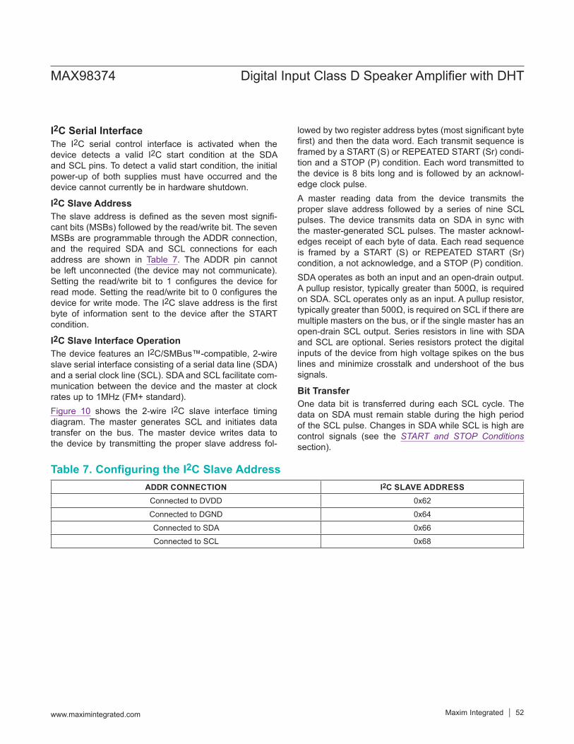
I2C Serial InterfaceThe I2C serial control interface is activated when the device detects a valid I2C start condition at the SDA and SCL pins. To detect a valid start condition, the initial power-up of both supplies must have occurred and the device cannot currently be in hardware shutdown.
I2C Slave AddressThe slave address is defined as the seven most signifi-cant bits (MSBs) followed by the read/write bit. The seven MSBs are programmable through the ADDR connection, and the required SDA and SCL connections for each address are shown in Table 7. The ADDR pin cannot be left unconnected (the device may not communicate).Setting the read/write bit to 1 configures the device for read mode. Setting the read/write bit to 0 configures the device for write mode. The I2C slave address is the first byte of information sent to the device after the START condition.
I2C Slave Interface OperationThe device features an I2C/SMBus™-compatible, 2-wire slave serial interface consisting of a serial data line (SDA) and a serial clock line (SCL). SDA and SCL facilitate com-munication between the device and the master at clock rates up to 1MHz (FM+ standard).Figure 10 shows the 2-wire I2C slave interface timing diagram. The master generates SCL and initiates data transfer on the bus. The master device writes data to the device by transmitting the proper slave address fol-
lowed by two register address bytes (most significant byte first) and then the data word. Each transmit sequence is framed by a START (S) or REPEATED START (Sr) condi-tion and a STOP (P) condition. Each word transmitted to the device is 8 bits long and is followed by an acknowl-edge clock pulse. A master reading data from the device transmits the proper slave address followed by a series of nine SCL pulses. The device transmits data on SDA in sync with the master-generated SCL pulses. The master acknowl-edges receipt of each byte of data. Each read sequence is framed by a START (S) or REPEATED START (Sr) condition, a not acknowledge, and a STOP (P) condition. SDA operates as both an input and an open-drain output. A pullup resistor, typically greater than 500Ω, is required on SDA. SCL operates only as an input. A pullup resistor, typically greater than 500Ω, is required on SCL if there are multiple masters on the bus, or if the single master has an open-drain SCL output. Series resistors in line with SDA and SCL are optional. Series resistors protect the digital inputs of the device from high voltage spikes on the bus lines and minimize crosstalk and undershoot of the bus signals.
Bit TransferOne data bit is transferred during each SCL cycle. The data on SDA must remain stable during the high period of the SCL pulse. Changes in SDA while SCL is high are control signals (see the START and STOP Conditions section).
Table 7. Configuring the I2C Slave AddressADDR CONNECTION I2C SLAVE ADDRESS
Connected to DVDD 0x62Connected to DGND 0x64Connected to SDA 0x66Connected to SCL 0x68
MAX98374 Digital Input Class D Speaker Amplifier with DHT
www.maximintegrated.com Maxim Integrated 52

START and STOP ConditionsSDA and SCL idle high when the bus is not in use. A mas-ter initiates communication by issuing a START condition. A START condition is a high-to-low transition on SDA with SCL high. A STOP condition is a low-to-high transi-tion on SDA while SCL is high. A START condition from the master signals the beginning of a transmission to the device. The master terminates transmission and frees the bus by issuing a STOP condition. The bus remains active if a REPEATED START condition is generated instead of a STOP condition.
Early STOP ConditionsThe device recognizes a STOP condition at any point during a data transmission, except if the STOP condition occurs in the same high pulse as a START condition. For proper operation, do not send a STOP condition during the same SCL high pulse as the START condition.
AcknowledgeThe acknowledge bit (ACK) is a clocked 9th bit that the device uses to handshake receipt each byte of data when in write mode (Figure 11). The device pulls down SDA during the entire master-generated 9th clock pulse if the previous byte is successfully received. Monitoring ACK allows for detection of unsuccessful data transfers. An unsuccessful data transfer occurs if a receiving device is busy or if a system fault has occurred. In the event of an unsuccessful data transfer, the bus master retries communication. The master pulls down SDA during the 9th clock cycle to acknowledge receipt of data when the device is in read mode. An acknowledge is sent by the master after each read byte to allow data transfer to con-tinue. A not-acknowledge is sent when the master reads the final byte of data from the device, followed by a STOP condition.
Figure 10. START, STOP, and REPEATED START Conditions
Figure 11. Acknowledge
SCL
SDA
ACKNOWLEDGE
CLOCK PULSE FOR ACKNOWLEDGMENTSTART
CONDITION
1 2 9
NOT ACKNOWLEDGE
MAX98374 Digital Input Class D Speaker Amplifier with DHT
www.maximintegrated.com Maxim Integrated 53

I2C Write Data FormatA write to the device includes transmission of a START condition, the slave address with the R/W bit set to 0, two bytes of data to configure the internal register address pointer, one or more bytes of data, and a STOP condition. Figure 12 illustrates the proper frame format for writing one byte of data to the device. Figure 13 illustrates the frame format for writing n-bytes of data to the device.The slave address with the R/W bit set to 0 indicates that the master intends to write data to the device. The device acknowledges receipt of the address byte during the master-generated 9th SCL pulse.
The second and third bytes transmitted from the master configure the device’s internal register address pointer. The pointer tells the device where to write the next byte of data. An acknowledge pulse is sent by the device upon receipt of the address pointer data.The third byte sent to the device contains the data that is written to the chosen register. An acknowledge pulse from the device signals receipt of the data byte. The address pointer auto-increments to the next register address after each received data byte. This auto-increment feature allows a master to write to sequential registers within one continuous frame. The master signals the end of trans-mission by issuing a STOP condition.
Figure 13. Writing n-Bytes of Data to the Slave
Figure 12. Writing One Byte of Data to the Slave
S 0 A A AREGISTER ADDRESS MSB REGISTER ADDRESS LSB DATA BYTE A P
1 BYTE
ACKNOWLEDGE FROM SLAVEACKNOWLEDGE FROM SLAVEACKNOWLEDGE FROM SLAVEB 7 B 6 B 5 B 4 B 3 B 2 B 1 B 0
ACKNOWLEDGE FROM SLAVE
AUTO-INCREMENT INTERNAL REGISTER ADDRESS POINTER
SLAVE ADDRESS
W SET INTERNAL ADDRESS POINTER
S 0 A A DATA BYTE
1 BYTE
ACKNOWLEDGE FROM SLAVEACKNOWLEDGE FROM SLAVEB 7 B 6 B 5 B 4 B 3 B 2 B 1 B 0
ACKNOWLEDGE FROM SLAVE
AUTO-INCREMENT INTERNAL REGISTER ADDRESS POINTER
SLAVE ADDRESS REGISTER ADDRESS
2 BYTES
DATA BYTE A
1 BYTE
B 7 B 6 B 5 B 4 B 3 B 2 B 1 B 0
ACKNOWLEDGE FROM SLAVE
AUTO-INCREMENT INTERNAL REGISTER ADDRESS POINTER
A P
REPEAT N TIMES
W
SET INTERNAL ADDRESS POINTER
MAX98374 Digital Input Class D Speaker Amplifier with DHT
www.maximintegrated.com Maxim Integrated 54

I2C Read Data FormatThe device address pointer must be preset to a specific register address before a read command is issued. The master presets the slave address pointer by first send-ing the slave device address with the R/W bit set to 0, followed by the desired slave register address. Then, to initiates a read operation, a REPEATED START condition is sent followed by the slave device address with the R/W bit set to 1. The slave acknowledges receipt of its slave address by pulling SDA low during the 9th SCL clock pulse. The slave would then transmit the contents of the register at the preset address. Transmitted slave data is valid on the rising edge of SCL.
In I2C slave mode, the device address pointer auto-increments after each read data byte. This auto-increment feature allows all device registers to be read sequentially within one continuous frame. A STOP condition can be issued after any number of read data bytes. The master acknowledges receipt of each read byte during the acknowledge clock pulse. The master must acknowledge all correctly received bytes except the last byte. The final byte must be followed by a not acknowledge from the master and then a STOP condition. Figure 14 illustrates the frame format for reading one byte from the device. Figure 15 illustrates the frame format for reading multiple bytes from the device.
Figure 14. Reading One Byte of Data from the Slave
Figure 15. Reading n-Bytes of Data from the Slave
S 0 A A
ACKNOWLEDGE FROM SLAVE
SLAVE ADDRESS REGISTER ADDRESS
2 BYTES
DATA BYTE A
1 BYTE
AUTO-INCREMENT INTERNAL REGISTER ADDRESS POINTER
W
SET INTERNAL ADDRESS POINTER
S r 1 A
ACKNOWLEDGE FROM SLAVE
SLAVE ADDRESS
R
NO ACKNOWLEDGE FROM MASTER
P
S 0 A A
ACKNOWLEDGE FROM SLAVE
SLAVE ADDRESS REGISTER ADDRESS
2 BYTES
DATA BYTE A
1 BYTE
AUTO-INCREMENT INTERNAL REGISTER ADDRESS POINTER
W
SET INTERNAL ADDRESS POINTER
S r 1 A
ACKNOWLEDGE FROM SLAVE
SLAVE ADDRESS
R
ACKNOWLEDGE FROM MASTER
DATA BYTE
1 BYTE
AUTO-INCREMENT INTERNAL REGISTER ADDRESS POINTER
P
REPEAT N TIMES
NO ACKNOWLEDGE FROM MASTER
A
MAX98374 Digital Input Class D Speaker Amplifier with DHT
www.maximintegrated.com Maxim Integrated 55

PCM InterfaceThe flexible PCM interface supports common sample rates from 16kHz to 96kHz, channel word lengths of 16-, 24-, and 32-bits, the standard I2S, left-justified, and TDM data formats.
PCM Clock ConfigurationThe digital audio interface defaults into PCM slave inter-face mode (INTERFACE_MODE bit field, Audio Interface Mode Configuration). The PCM slave interface requires the host to supply both BCLK and LRCLK. To configure the PCM interface clock inputs, the host must program both the device sample rate and BCLK to LRCLK ratio.
Clock Ratio ConfigurationThe PCM interface sample rate must be configured to match the frequency of the frame clock (LRCLK) using the PCM_SR registers. The speaker path sample rate (SPK_SR) and the PCM interface sample rate (PCM_SR) must be configured by the host to be the same.The device supports a range of BCLK to LRCLK clock ratios (PCM_BSEL) ranging from 32 to 512. However, based on the selected PCM interface sample rate (LRCLK frequency), the configured clock ratio cannot result in a BLCK frequency that exceeds 15.36MHz.
Audio Interface Mode ConfigurationREGISTER ADDRESS = 0x2025
DESCRIPTIONBIT PoR BIT NAME TYPE RES7 0
RESERVED — — UnusedReturns 0 if read.
6 05 04 03 02 0
1 0INTERFACE_
MODE[1:0] RW-S EN
Audio Interface ModeSelects the digital audio data interface mode. 00 = PCM slave interface mode (BCLK input, LRCLK input) 01 = Reserved10 = Reserved11 = SoundWire slave interface mode (SWCLK input)
0 0
MAX98374 Digital Input Class D Speaker Amplifier with DHT
www.maximintegrated.com Maxim Integrated 56

PCM Interface Sample Rate
Speaker Path Sample Rate
REGISTER ADDRESS = 0x2027DESCRIPTION
BIT PoR BIT NAME TYPE RES7 0
RESERVED — — UnusedReturns 0 if read.
6 05 04 0
3 1
PCM_SR[3:0] RW-S EN
PCM Sample RateSets the sample rate of the PCM interface. This corresponds to the input or desired LRCLK frequency. 0000-0010 = Reserved0011 = 16kHz0100 = 22.05kHz0101 = 24kHz0110 = 32kHz0111 = 44.1kHz1000 = 48kHz1001 = 88.2kHz1010 = 96kHz1011 to 1111 = Reserved
2 0
1 0
0 0
REGISTER ADDRESS = 0x2028DESCRIPTION
BIT PoR BIT NAME TYPE RES
7 1
SPK_SR[3:0] RW-S EN
Speaker Amplifier Path Sample RateSets the sample rate of the speaker amplifier path.0000-0010 = Reserved0011 = 16kHz0100 = 22.05kHz0101 = 24kHz0110 = 32kHz0111 = 44.1kHz1000 = 48kHz1001 = 88.2kHz1010 = 96kHz1011 to 1111 = Reserved
6 0
5 0
4 0
3 1
RESERVED — — Unused 2 0
1 0
0 0
MAX98374 Digital Input Class D Speaker Amplifier with DHT
www.maximintegrated.com Maxim Integrated 57

PCM Data Format ConfigurationThe device supports the standard I2S, left-justified, TDM data formats, and the operating mode is configured using the PCM_FORMAT bit field.
I2S and Left-Justified ModeI2S and left-justified formats support two channels that can be 16, 24, or 32 bits in length. The BCLK to LRCLK ratio (PCM_BSEL) must be configured to be twice the desired channel length. The audio data word size is configurable to 16, 24, or 32 bits in length (PCM_DATA_WIDTH), but must be programmed to be less than or equal to the channel length. If the resulting channel length exceeds
the configured data word size, then the data input LSBs are truncated and the data output LSBs are padded with either zero or Hi-Z data based on the PCM_TX_CHm_HIZ register bit setting.With the default PCM settings, falling LRCLK indicates the start of a new frame and the left channel data (chan-nel 0) while rising LRCLK indicates the right channel data (channel 1). In I2S mode, the MSB of the audio word is latched on the second active BCLK edge after an LRCLK transition. In left-justified mode, the MSB of the audio word is latched on the first active BCLK edge after an LRCLK transition.
PCM Interface Clock Ratio Configuration
Table 8. Supported I2S/Left-Justified Mode Configurations
REGISTER ADDRESS = 0x2026DESCRIPTION
BIT PoR BIT NAME TYPE RES7 0
RESERVED — — UnusedReturns 0 if read.6 0
5 0
4 0 PCM_BCLKEDGE RW-S EN
Active BCLK Edge ControlSelects the active BCLK edge.0 = Data captured and valid on rising edge of BCLK.1 = Data captured and valid on falling edge of BCLK.
3 0
PCM_BSEL[3:0] RW-S EN
BCLK to LRCLK RatioSelects the number of BCLKs per LRCLK for PCM.0000 to 0001 = Reserved0010 = 320011 = 480100 = 640101 = 960110 = 1280111 = 1921000 = 2561001 = 3841010 = 5121011 = 3201100 to 1111 = Reserved
2 1
1 0
0 0
CHANNELS CHANNEL LENGTH
BCLK TO LRCLK RATIO (PCM_BSEL)
SUPPORTED DATA WORD SIZES (PCM_DATA_WIDTH)
216 32 1624 48 16, 2432 64 16, 24, 32
MAX98374 Digital Input Class D Speaker Amplifier with DHT
www.maximintegrated.com Maxim Integrated 58
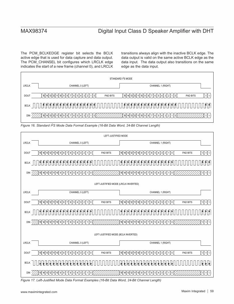
The PCM_BCLKEDGE register bit selects the BCLK active edge that is used for data capture and data output. The PCM_CHANSEL bit configures which LRCLK edge indicates the start of a new frame (channel 0), and LRCLK
transitions always align with the inactive BCLK edge. The data output is valid on the same active BCLK edge as the data input. The data output also transitions on the same edge as the data input.
Figure 16. Standard I2S Mode Data Format Example (16-Bit Data Word, 24-Bit Channel Length)
Figure 17. Left-Justified Mode Data Format Examples (16-Bit Data Word, 24-Bit Channel Length)
STANDARD I2S MODE
LRCLK
12131415 891011 4567 0123 PAD BITS
CHANNEL 0 (LEFT) CHANNEL 1 (RIGHT)
DOUT
BCLK
DIN
12131415 891011 4567 0123 PAD BITS 1415
12131415 891011 4567 0123 12131415 891011 4567 0123 1415
LRCLK
12131415 891011 4567 0123 PAD BITS
CHANNEL 0 (LEFT) CHANNEL 1 (RIGHT)
DOUT
BCLK
DIN
LEFT-JUSTIFIED MODE
12131415 891011 4567 0123 PAD BITS 1415
12131415 891011 4567 0123 12131415 891011 4567 0123 1415
LEFT-JUSTIFIED MODE (LRCLK INVERTED)
LEFT-JUSTIFIED MODE (BCLK INVERTED)
13
13
LRCLK
12131415 891011 4567 0123 PAD BITS
CHANNEL 0 (LEFT) CHANNEL 1 (RIGHT)
DOUT
BCLK
DIN
12131415 891011 4567 0123 PAD BITS 1415
12131415 891011 4567 0123 12131415 891011 4567 0123 1415
13
13
LRCLK
12131415 891011 4567 0123 PAD BITS
CHANNEL 0 (LEFT) CHANNEL 1 (RIGHT)
DOUT
BCLK
DIN
12131415 891011 4567 0123 PAD BITS 1415
12131415 891011 4567 0123 12131415 891011 4567 0123 1415
13
13
MAX98374 Digital Input Class D Speaker Amplifier with DHT
www.maximintegrated.com Maxim Integrated 59

TDM ModesThe provided TDM modes support up to 16 audio chan-nels of 16-, 24-, or 32-bit data each. The number of TDM channels is determined by both the selected BCLK to LRCLK ratio (PCM_BSEL) and the selected data word size (PCM_DATA_WIDTH). In TDM mode, the channel length and data word size are always equal.With the default PCM interface settings, in TDM mode a rising frame clock (LRCLK) edge acts as the frame sync pulse and indicates the start of a new frame. The frame sync pulse width must be equal to at least one bit clock period; however, the falling edge can occur at any time if it does not violate the setup time of the next frame sync
pulse rising edge. The PCM_CHANSEL bit can be used to invert the LRCLK edges (sync pulse) used to start a TDM frame.In TDM mode, the MSB of the first audio word can be latched on the first, second, or third active BCLK edge after the sync pulse and is programmed by the PCM_FORMAT bits (TDM mode 0, 1, and 2). Additionally, the PCM_BCLKEDGE register bit allows for programmability of the BCLK edge that is used for data capture and data output. The data output is valid on the same active BCLK edge as the data input. The data output also transitions on the same edge as data input.
Table 9. Supported TDM Mode Configurations
CHANNELS DATA WORD SIZES (PCM_DATA_WIDTH)
BCLK TO LRCLK RATIO (PCM_BSEL)
MAXIMUM SUPPORTED SAMPLE RATE (fLRCLK) (kHz)
216 32
96
24 4832 64
416 6424 9632 128
816 12824 192
4832 256
10 32 320
1616 25624 384 3232 512 24
MAX98374 Digital Input Class D Speaker Amplifier with DHT
www.maximintegrated.com Maxim Integrated 60

Figure 18. TDM Mode Data Format Examples (4 Channels, 32-Bit Data Word and Channel Length)
LRCLK
28293031 0123
CHANNEL 0 (32 BITS)
DOUT
BCLK
DIN
3031 2928293031 0123 28293031 0123 28293031 012301
CHANNEL 1 (32 BITS) CHANNEL 2 (32 BITS) CHANNEL 3 (32 BITS)
28293031 0123 3031 2928293031 0123 28293031 0123 28293031 012301
LRCLK
28293031 0123
CHANNEL 0 (32 BITS)
DOUT
BCLK
DIN
303128293031 0123 28293031 0123 28293031 012301
CHANNEL 1 (32 BITS) CHANNEL 2 (32 BITS) CHANNEL 3 (32 BITS)
28293031 0123 303128293031 0123 28293031 0123 28293031 012301
2
2
LRCLK
28293031 0123
CHANNEL 0 (32 BITS)
DOUT
BCLK
DIN
3128293031 0123 28293031 0123 28293031 012301
CHANNEL 1 (32 BITS) CHANNEL 2 (32 BITS) CHANNEL 3 (32 BITS)
28293031 0123 3128293031 0123 28293031 0123 28293031 012301
2
2
LRCLK
28293031 0123
CHANNEL 0 (32 BITS)
DOUT
BCLK
DIN
3031 2928293031 0123 28293031 0123 28293031 012301
CHANNEL 1 (32 BITS) CHANNEL 2 (32 BITS) CHANNEL 3 (32 BITS)
28293031 0123 3031 2928293031 0123 28293031 0123 28293031 012301
3
3
TDM MODE 0 (BCLK INVERTED)
TDM MODE 1
TDM MODE 2
TDM MODE 0
MAX98374 Digital Input Class D Speaker Amplifier with DHT
www.maximintegrated.com Maxim Integrated 61

PCM Interface Data Format ConfigurationREGISTER ADDRESS = 0x2024
DESCRIPTIONBIT PoR BIT NAME TYPE RES
7 1PCM_DATA_ WIDTH[1:0] RW-R PCM
Data Word Size ControlConfigures the PCM data word size for each channel.00 = Reserved01 = 16-Bit10 = 24-Bit11 = 32-Bit
6 1
5 0
PCM_FORMAT[2:0] RW-R PCM
PCM Format SelectSelects the PCM data format.000 = I2S mode001 = Left-justified010 = Reserved011 = TDM mode 0 (0 BCLK delay from LRCLK)100 = TDM mode 1 (1 BCLK delay from LRCLK)101 = TDM mode 2 (2 BCLK delay from LRCLK)110 to 111 = Reserved
4 0
3 0
2 0 RESERVED — — Unused - Returns 0 if read
1 0 PCM_CHANSEL RW-R PCM
Active LRCLK Edge ControlSelects which LRCK edge starts a new frame (channel 0).0 = In I2S and LJ modes: falling LRCLK edge starts a new frame.In TDM modes: rising LRCLK edge starts a new frame.1 = In I2S and LJ modes: rising LRCLK edge starts a new frame.In TDM modes: falling LRCLK edge starts a new frame.
0 0 PCM_TX_EXTRA_HIZ RW-R PCM
Extra BCLK Cycles Hi-Z ControlSelect whether DOUT is driven to zero or Hi-Z during extra BCLK cycles.0 = Drive DOUT to zero for extra BCLK cycles.1 = Drive DOUT to Hi-Z for extra BCLK cycles.
MAX98374 Digital Input Class D Speaker Amplifier with DHT
www.maximintegrated.com Maxim Integrated 62
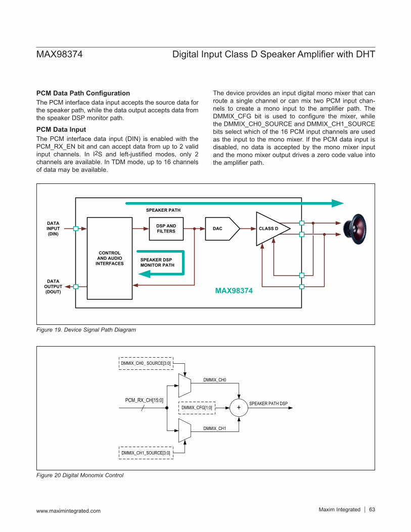
PCM Data Path ConfigurationThe PCM interface data input accepts the source data for the speaker path, while the data output accepts data from the speaker DSP monitor path.
PCM Data InputThe PCM interface data input (DIN) is enabled with the PCM_RX_EN bit and can accept data from up to 2 valid input channels. In I2S and left-justified modes, only 2 channels are available. In TDM mode, up to 16 channels of data may be available.
The device provides an input digital mono mixer that can route a single channel or can mix two PCM input chan-nels to create a mono input to the amplifier path. The DMMIX_CFG bit is used to configure the mixer, while the DMMIX_CH0_SOURCE and DMMIX_CH1_SOURCE bits select which of the 16 PCM input channels are used as the input to the mono mixer. If the PCM data input is disabled, no data is accepted by the mono mixer input and the mono mixer output drives a zero code value into the amplifier path.
Figure 19. Device Signal Path Diagram
Figure 20 Digital Monomix Control
DATA INPUT (DIN)
SPEAKER PATH
SPEAKER DSP MONITOR PATH
MAX98374DATA
OUTPUT (DOUT)
DSP AND FILTERS DAC CLASS D
CONTROL AND AUDIO
INTERFACES
SPEAKER PATH DSP
DMMIX_CH0_ SOURCE[3:0]
PCM_RX_CH[15:0]
DMMIX_CH1
DMMIX_CH0
+
DMMIX_CH1_SOURCE[3:0]
DMMIX_CFG[1:0]
MAX98374 Digital Input Class D Speaker Amplifier with DHT
www.maximintegrated.com Maxim Integrated 63

PCM Interface Data Input (DIN) Enable
PCM Interface Digital Mono Mixer Configuration 1
REGISTER ADDRESS = 0x202BDESCRIPTION
BIT PoR BIT NAME TYPE RES7 0
RESERVED — — UnusedReturns 0 if read.
6 05 04 03 02 01 0
0 0 PCM_RX_EN RW-R SFB
PCM Receiver EnableEnables the data input (DIN) of the PCM interface.0 = PCM data input disabled1 = PCM data input enabled
REGISTER ADDRESS = 0x2029DESCRIPTION
BIT PoR BIT NAME TYPE RES
7 0
DMMIX_CFG[1:0] RW-R SFB
Mono Mixer ConfigurationDetermines the behavior of the mono mixer circuit.00 = Output of mono mixer is channel 001 = Output of mono mixer is channel 110 = Output of mono mixer is (channel 0 + channel 1)/211 = Reserved
6 0
5 0RESERVED — — Unused
Returns 0 if read.4 0
3 0
DMMIX_CH0_SOURCE[3:0] RW-R SFB
Mono Mixer Channel 0 Source SelectSelects which PCM interface data input channel is assigned to channel 0 of the digital mono mixer.0000 = Channel 0 gets PCM interface data input channel 0.0001 = Channel 0 gets PCM interface data input channel 1.....1110 = Channel 0 gets PCM interface data input channel 14.1111 = Channel 0 gets PCM interface data input channel 15.
2 0
1 0
0 0
MAX98374 Digital Input Class D Speaker Amplifier with DHT
www.maximintegrated.com Maxim Integrated 64

PCM Data OutputThe PCM interface data output (DOUT) is enabled by the PCM_TX_EN bit and can drive output data onto any valid enabled output channel. In I2S and left-justified modes, only 2 output channels are available. In TDM mode, up to 16 output channels may be available.It is possible to output the result of the speaker amplifier path DSP (taken at the input to the DAC) to the PCM Interface output by enabling the SPK_FB_EN and PCM_ SPK_FB_DEST register bits. The host can use this to
monitor the data that is being driven into the DAC (after the digital volume, BDE, etc.). It is invalid for SPK_FB_EN to be 1 while SPK_EN is 0.If an output channel is enabled and no data source is assigned to it, then the output data is all zeros. The PCM data output is Hi-Z if the device is disabled (EN = 0), the PCM data output is disabled (PCM_TX_EN = 0), or all output channels are set to a Hi-Z output (All PCM_TX_CHn_HIZ = 1). A summary of the controls for the PCM data output (DOUT) are shown in Table 10.
Table 10. Control Registers and the DOUT Pin
* A channel is selected if a path is both enabled and its destination bit field corresponds to that channel.
PCM Interface Digital Mono Mixer Configuration 2REGISTER ADDRESS = 0x202A
DESCRIPTIONBIT PoR BIT NAME TYPE RES7 0
RESERVED — — UnusedReturns 0 if read.
6 05 04 0
3 0
DMMIX_CH1_SOURCE[3:0] RW-R SFB
Mono Mixer Channel 1 Source SelectSelects which PCM interface data input channel is assigned to channel 1 of the digital mono mixer.0000 = Channel 1 gets PCM interface data input channel 0.0001 = Channel 1 gets PCM interface data input channel 1.....1110 = Channel 1 gets PCM interface data input channel 14.1111 = Channel 1 gets PCM interface data input channel 15.
2 0
1 0
0 0
EN PCM_TX_CH_EN PCM_TX_CHn_HIZ CHANNEL n SELECTED AS THE DESTINATION FOR PATH* DOUT FOR CHANNEL n
0 — — — Hi-Z (all channels)1 0 — — Hi-Z (all channels)1 1 1 — Hi-Z (channel n)1 1 0 No 0 (channel n)1 1 0 Yes Data (channel n)
MAX98374 Digital Input Class D Speaker Amplifier with DHT
www.maximintegrated.com Maxim Integrated 65

PCM Interface Data Output (DOUT) Enable
PCM Interface Data Output Speaker DSP Feedback Channel Source
REGISTER ADDRESS = 0x202CDESCRIPTION
BIT PoR BIT NAME TYPE RES7 0
RESERVED — — UnusedReturns 0 if read.
6 05 04 03 02 01 0
0 0 PCM_TX_EN RW-D —
PCM Transmitter EnableEnables the data output (DOUT) of the PCM interface.0 = PCM data output disabled1 = PCM data output enabled
REGISTER ADDRESS = 0x2023DESCRIPTION
BIT PoR BIT NAME TYPE RES7 0
RESERVED — — UnusedReturns 0 if read.
6 05 04 0
3 0
PCM_SPK_FB_DEST[3:0] RW-R FB
Speaker Amplifier DSP to PCM Feedback DestinationPCM data output channel selection for the speaker amplifier DSP to PCM feedback path.0000 = PCM channel 00001 = PCM channel 1... = ...1110 = PCM channel 141111 = PCM channel 15
2 0
1 0
0 0
MAX98374 Digital Input Class D Speaker Amplifier with DHT
www.maximintegrated.com Maxim Integrated 66

PCM Interface Data Output Channel Configuration 1REGISTER ADDRESS = 0x2020
DESCRIPTIONBIT PoR BIT NAME TYPE RES
7 1 PCM_TX_CH7_HIZ RW-R TXENPCM Transmit Channel 7 Hi-Z Configuration0 = Transmit channel 7 output is data/zeros1 = Transmit channel 7 output is Hi-Z
6 1 PCM_TX_CH6_HIZ RW-R TXENPCM Transmit Channel 6 Hi-Z Configuration0 = Transmit channel 6 output is data/zeros1 = Transmit channel 6 output is Hi-Z
5 1 PCM_TX_CH5_HIZ RW-R TXENPCM Transmit Channel 5 Hi-Z Configuration0 = Transmit channel 5 output is data/zeros1 = Transmit channel 5 output is Hi-Z
4 1 PCM_TX_CH4_HIZ RW-R TXENPCM Transmit Channel 4 Hi-Z Configuration0 = Transmit channel 4 output is data/zeros1 = Transmit channel 4 output is Hi-Z
3 1 PCM_TX_CH3_HIZ RW-R TXENPCM Transmit Channel 3 Hi-Z Configuration0 = Transmit channel 3 output is data/zeros1 = Transmit channel 3 output is Hi-Z
2 1 PCM_TX_CH2_HIZ RW-R TXENPCM Transmit Channel 2 Hi-Z Configuration0 = Transmit channel 2 output is data/zeros1 = Transmit channel 2 output is Hi-Z
1 1 PCM_TX_CH1_HIZ RW-R TXENPCM Transmit Channel 1 Hi-Z Configuration0 = Transmit channel 1 output is data/zeros1 = Transmit channel 1 output is Hi-Z
0 0 PCM_TX_CH0_HIZ RW-R TXENPCM Transmit Channel 0 Hi-Z Configuration0 = Transmit channel 0 output is data/zeros1 = Transmit channel 0 output is Hi-Z
MAX98374 Digital Input Class D Speaker Amplifier with DHT
www.maximintegrated.com Maxim Integrated 67

PCM Interface Data Output Channel Configuration 2REGISTER ADDRESS = 0x2021
DESCRIPTIONBIT PoR BIT NAME TYPE RES
7 1 PCM_TX_CH15_HIZ RW-R TXENPCM Transmit Channel 15 Hi-Z Configuration0 = Transmit channel 15 output is data/zeros1 = Transmit channel 15 output is Hi-Z
6 1 PCM_TX_CH14_HIZ RW-R TXENPCM Transmit Channel 14 Hi-Z Configuration0 = Transmit channel 14 output is data/zeros1 = Transmit channel 14 output is Hi-Z
5 1 PCM_TX_CH13_HIZ RW-R TXENPCM Transmit Channel 13 Hi-Z Configuration0 = Transmit channel 13 output is data/zeros1 = Transmit channel 13 output is Hi-Z
4 1 PCM_TX_CH12_HIZ RW-R TXENPCM Transmit Channel 12 Hi-Z Configuration0 = Transmit channel 12 output is data/zeros1 = Transmit channel 12 output is Hi-Z
3 1 PCM_TX_CH11_HIZ RW-R TXENPCM Transmit Channel 11 Hi-Z Configuration0 = Transmit channel 11 output is data/zeros1 = Transmit channel 11 output is Hi-Z
2 1 PCM_TX_CH10_HIZ RW-R TXENPCM Transmit Channel 10 Hi-Z Configuration0 = Transmit channel 10 output is data/zeros1 = Transmit channel 10 output is Hi-Z
1 1 PCM_TX_CH9_HIZ RW-R TXENPCM Transmit Channel 9 Hi-Z Configuration0 = Transmit channel 9 output is data/zeros1 = Transmit channel 9 output is Hi-Z
0 1 PCM_TX_CH8_HIZ RW-R TXENPCM Transmit Channel 8 Hi-Z Configuration0 = Transmit channel 8 output is data/zeros1 = Transmit channel 8 output is Hi-Z
MAX98374 Digital Input Class D Speaker Amplifier with DHT
www.maximintegrated.com Maxim Integrated 68

SoundWire Slave InterfaceWhen in SoundWire mode, the SoundWire compatible slave interface supports both audio and control data transport over the shared 2-wire bus comprising a clock input (SWCLK) and a bidirectional data input/output (SWDATA). For device configuration, the SoundWire mas-ter can access both the general control and SoundWire slave interface registers. The SoundWire slave interface receives and routes all enabled device status interrupts to the SoundWire master for servicing.Set the INTERFACE_MODE bit field (Audio Interface Mode Configuration) to 0x3 to select SoundWire slave interface mode for digital audio data. For speaker path play-back, the SoundWire compatible slave interface provides an input data port that accepts stereo PCM audio data.
SoundWire Slave Device Identification and AddressingThe SoundWire compatible slave interface provides a 48-bit value (Device_Id[47:0] in the SCP_DevId_0 to SCP_DevId_5 registers) that is read by the SoundWire Master to identify the connected SoundWire slave device. The SoundWire slave device identification bit field con-tains multiple segments each detailed in Table 11. All segments are fixed except for the slave device unique ID.The 4-bit SoundWire slave device unique ID (Device_Id[43:40]) is pin configurable and has eight possible combinations. To select the device unique ID, connect the ADDR, SDA, and SCL pins as shown in Table 12.
Table 11. SoundWire Slave Device Identification
Table 12. SoundWire Slave Device Unique ID Configuration
REGISTER BIT FIELD SEGMENT DESCRIPTION VALUE
SCP_DevId_0Device_Id[47:44] SoundWire Version Number 0x2Device_Id[43:40] Slave Device Unique ID Decoded From Pin 0x0 to 0x8
SCP_DevId_1 and SCP_DevId_2 Device_Id[39:24] MIPI Assigned Manufacturer ID 0x019F
SCP_DevId_3 and SCP_DevId_4 Device_Id[23:8] Audio Part Number (OTP Programmable) 0x8374
SCP_DevId_5 Device_Id[7:0] Class—MIPI Reserved 0x00
ADDR PIN SDA PIN SCL PIN DEVICE UNIQUE IDConnect to DGND Connect to DGND Connect to DGND 0x1Connect to DGND Connect to DVDD Connect to DGND 0x2Connect to DGND Connect to DGND Connect to DVDD 0x3Connect to DGND Connect to DVDD Connect to DVDD 0x4Connect to DVDD Connect to DVDD Connect to DVDD 0x5Connect to DVDD Connect to DVDD Connect to DGND 0x6Connect to DVDD Connect to DGND Connect to DVDD 0x7Connect to DVDD Connect to DGND Connect to DGND 0x8
MAX98374 Digital Input Class D Speaker Amplifier with DHT
www.maximintegrated.com Maxim Integrated 69

SoundWire Clock ConfigurationThe SoundWire compatible slave interface operates and supports device programming with any valid input SoundWire clock frequency (as specified in version 1.1 of the SoundWire specification). However, in this mode, the external SoundWire clock is also the source clock for all internal clock generation (Figure 21).Therefore, for the device audio and data paths to oper-ate, the external SoundWire clock frequency must either
match or be an integer divider (2/4/8) of one of the sup-ported input clock frequencies. The expected SoundWire input clock frequency is programmed using the input clock configuration register (SoundWire Input Clock Configuration). The SoundWire clock frequency selection and rate divider are calculated with the following formula:
S W C LKS W IR E _ C LK _ S E L[2 : 0 ]f
S W IR E _ C LK _R A T E[1 : 0 ]=
Figure 21. Internal Clock Generation in SoundWire Control Mode
SoundWire Input Clock Configuration
SOUNDWIRE CLOCK INPUT
SOUNDWIRECOMPATIBLE
SLAVE INTERFACE
SWIRE_CLK_SELSWIRE_CLK_RATE
TO INTERNAL CONVERTERS/
DSP/ETC.
INTERNAL CLOCK
GENERATION
CLOCK SELECTION/SCALING
REGISTER ADDRESS = 0x2036DESCRIPTION
BIT PoR BIT NAME TYPE RES7 0
RESERVED — — Unused Returns 0 if read.6 0
5 0
4 0
SWIRE_CLK_RATE[1:0] RW-S EN
SoundWire Input Clock Rate DividerSelects the SoundWire input clock rate divider. The SoundWire clock frequency must match the clock family selected divided by this setting.00: Divide by 1 (default) 10: Divide by 401: Divide by 2 11: Divide by 83 0
2 1
SWIRE_CLK_SEL[2:0] RW-S EN
SoundWire Input Clock Frequency FamilySelects the SoundWire input clock frequency family. The input clock frequency must match or be a supported integer divided by this setting. Note: The 13MHz clock family requires a divider of either 2 or 4.000: 7.68Mhz 100: 12.00Mhz001: 8.40Mhz 101: 12.288Mhz010: 9.60Mhz 110: 13.00Mhz011: 11.2896Mhz 111: Reserved
1 0
0 1
MAX98374 Digital Input Class D Speaker Amplifier with DHT
www.maximintegrated.com Maxim Integrated 70

SoundWire Slave Control Port (SCP) ConfigurationThe device SCP supports the options shown in Table 13. The SCP configuration bit fields are in the SoundWire slave interface registers from address 0x0040 to address 0x0070. For detailed register and bit field descriptions, reference the full MIPI SoundWire® Specification (Version 1.1).
SoundWire Device Data Port (DP) ConfigurationThe SoundWire slave interface provides four data ports, each of which is described in Table 14.The speaker path and amplifier DSP path data ports support all data flow modes (Isochronous, Tx-Controlled, Rx-Controlled, Full-Asynchronous). Data port test modes (Normal, PRBS, Static-0, and Static-1) are provided.
When operating as a passive slave (device is attached to the SoundWire bus but all data ports are deactivated) the interface is optimized to minimize power consumption, and only the logic cells that need to be active are switching. Data port power is managed using the SoundWire defined Prepare-Ready-Activate mechanism. The SoundWire mas-ter should only enable and disable slave interface data ports while the device is in software shutdown.The provided data ports support a subset of options as shown in Table 15. The data port control bit fields are located in the SoundWire slave interface registers from address 0x0100 to address 0x0337. For detailed reg-ister and bit field descriptions, reference the full MIPI SoundWire® Specification (Version 1.1).
Table 13. SoundWire Slave Control Port (SCP) Options
Table 14. SoundWire Slave Interface Data Port Assignments
Table 15. Data Port 1 and 3 Options
SLAVE CONTROL PORT OPTION PROVIDEDImplementation Defined Interrupt 1 Yes
Clock-Stop Mode 1 YesClock-Stop Prepare State Machine SimplifiedClock-Stop Asynchronous Wake Up No
Address Paging NoMulti-Lane NoBridging NoHigh Phy NoTest Mode No
Broadcast Read Response Command Ignored
NUMBER DIRECTION TYPE CHANNELS WORD SIZE FUNCTIONData Port 0 — — — — Not SupportedData Port 1 Rx (Input) Full 2 32-Bit Data Input for the Speaker PathData Port 2 — — — — Not SupportedData Port 3 Tx (Output) Full 2 16-Bit Data Output for amplifier DSP path
Data Ports 4-14 — — — — Not Supported
DATA PORT OPTIONS PROVIDEDImplementation defined Interrupt 1 NoImplementation defined Interrupt 2 NoImplementation defined Interrupt 3 No
Flow Mode Support YesExtended Buffer Operating Modes for Flow Control No
Block Group Support NoPrepare State Machine Advanced
MAX98374 Digital Input Class D Speaker Amplifier with DHT
www.maximintegrated.com Maxim Integrated 71

InterruptsThe device supports individually enabled status interrupts for sending feedback to the host about events that have occurred on-chip. When enabled, interrupts are transmit-ted on the IRQ output in I2C control mode and through the SoundWire slave interface in SoundWire control mode.
Interrupt Bit Field CompositionEach interrupt source has five individual bit field compo-nents. The function of each component is detailed below and the corresponding bit fields for each source can be identified by the appended suffix (shown in parentheses).
Raw Status (RAW)Each interrupt source has a read-only bit to indicate the real-time raw status of the interrupt source.
State (STATE)Each interrupt source has a read-only state bit that is set whenever a rising edge occurs on the associated raw status bit. The state bit is set regardless of the setting of the source enable bit.
Flag (FLAG)Each interrupt source has a read-only flag bit. If the source enable bit is set, then the flag bit is set, and an interrupt can be generated whenever the source state bit is set.
Enable (EN)Each interrupt source has a dynamic read/write enable bit. When the enable bit is set, the associated flag bit is set, and an interrupt can be generated whenever the source state bit is set.
Clear (CLR)Each interrupt source has a dynamic write-only clear bit. Writing a 1 to a clear bit resets the associated state and flag bits to 0. Writing a 0 to a clear bit has no effect. In I2C con-trol mode, the IRQ output is deasserted if all flag bits are 0.
IRQ Output ConfigurationThe device allows the user to configure the drive mode and polarity of the IRQ output. The IRQ_MODE bit con-trols the drive mode. If IRQ_MODE is 0, the pin is config-ured as an open-drained output and requires an external pullup resistor. If IRQ_MODE is 1, then IRQ is configured as a push-pull CMOS output.The IRQ_POL bit controls the polarity of the IRQ bus. Interrupt events (a flag bit is set high) assert the IRQ bus low if IRQ_POL = 0 and high if IRQ_POL = 1. The IRQ bus deasserts if all flag bits are cleared (set low).
Interrupt SourcesThe events in Device Interrupt Sources can cause device interrupts when enabled (corresponding interrupt enable set high).
IRQ Bus ConfigurationREGISTER ADDRESS = 0x2010
DESCRIPTIONBIT PoR BIT NAME TYPE RES7 0
RESERVED — —Unused Returns 0 if read.
6 05 04 03 0
2 0 IRQ_MODE RW-R IRQ
IRQ ModeControls the drive mode of the IRQ Output. 0 = Open-drain output (an external pullup resistor is necessary)1 = CMOS push-pull output
1 0 IRQ_POL RW-R IRQ
IRQ PolarityControls the IRQ bus polarity.0 = Low when any interrupt FLAG bits are high1 = High when any interrupt FLAG bits are high
0 0 IRQ_EN RW-D —
IRQ EnableEnables the IRQ Output. 0 = IRQ output is disabled and is high-impedance1 = IRQ output is enabled and is controlled by the interrupt controller
MAX98374 Digital Input Class D Speaker Amplifier with DHT
www.maximintegrated.com Maxim Integrated 72

Device Interrupt SourcesREGISTER ADDRESS
INTERRUPT SOURCES BIT FIELD DESCRIPTION
0x20010x20040x20070x200A0x200D
BDE Active Begin Event BDE_ACTIVE_BGN_* Indicates that the BDE is active.BDE Active End Event BDE_ACTIVE _END_* Indicates that the BDE is no longer active.
BDE Level Change Event BDE_LEVEL_* Indicates that the BDE has transitioned between thresholds.BDE Level 4 Event BDE_L4_* Indicated that the BDE has transitioned into level 4.
Thermal WarningBegin Event THERMWARN_BGN_* Indicates when the thermal-warning threshold has been
exceeded.
Thermal Warning End Event THERMWARN_END_*
Indicates that the die temperature was previously above the thermal-warning threshold and has now dropped below the threshold.
Thermal Shutdown Begin Event THERMSHDN_BGN_* Indicates when the thermal-shutdown threshold has been
exceeded.
Thermal Shutdown End Event THERMSHDN_END_*
Indicates that the die temperature was previously above the thermal-shutdown threshold and has now dropped below the threshold.
0x20020x20050x20080x200B0x200E
ICC Data Error ICC_DATA_ERR_* Indicates that the ICC synchronization lock for the assigned group was broken due to incorrect data.
ICC Synchronization Error ICC_SYNC_ERR_*
Indicates that the device has not synchronized within the ICC time-out period from when the ICC interface was enabled.
Clock Monitor Start Event CLKSTART_* Indicates that the clock monitor has detected a restart of
clock.
Clock Monitor Stop Event CLKSTOP_* Indicates that the clock monitor has detected a loss of
clock.
Speaker OverCurrent Event SPK_OVC_* Indicates that the speaker amplifier current limit has been
exceeded.
Power-Up Done Event PWRUP_DONE_* Indicates when the device has completed power-up successfully.
Power-Down Done Event PWRDN_DONE_* Indicates when the device has completed power-down.
OTP Load Fail Event OTP_FAIL_* Indicates when the OTP load routine that runs when exiting hardware shutdown has failed to complete successfully.
MAX98374 Digital Input Class D Speaker Amplifier with DHT
www.maximintegrated.com Maxim Integrated 73

Digital Output Pin Drive StrengthThe drive strength control (*_DRV) bits set the drive strengths of the logic output pins. Four different CMOS drive strengths are available for each logic output (Digital Output Pin Drive Strength Configuration).
Device Interrupt Sources (continued)
Note: The bit fields are shown without the component suffixes. For example, BDE_LEVEL_* refers to BDE_LEVEL_RAW, BDE_LEVEL_STATE, BDE_LEVEL_FLAG, BDE_LEVEL_EN, and BDE_LEVEL_CLR. All Interrupt sources have these five component bit fields.
Digital Output Pin Drive Strength Configuration
REGISTER ADDRESS
INTERRUPT SOURCES BIT FIELD DESCRIPTION
0x20030x20060x20090x200C0x200F
Limiter Active Begin Event LMTR_ACTIVE_BGN_* Indicates that the limiter circuit is applying a hard limit
(infinite compression) to the signal.Limiter Active
End Event LMTR_ACTIVE_END_* Indicates that the limiter circuit has stopped applying a hard limit (infinite compression) to the signal.
DHT Active Begin Event DHT_ACTIVE_BGN_* Indicates that the DHT circuit is active and is applying
compression to the signal.DHT Active End Event DHT_ACTIVE_END_* Indicates that the DHT circuit has stopped applying
compression to the signal.Thermal Foldback
Begin Event THERMFB_BGN_* Indicates die temperature is above thermal-foldback threshold and device is attenuating the output.
Thermal Foldback End Event THERMFB_END_* Indicates die temperature is below thermal-foldback
threshold and device has stopped attenuating the output.PVDD UVLO
Shutdown Event PVDD_UVLO_SHDN_* Indicates that PVDD has dropped below the minimum allowed voltage after initial power-up is complete.
REGISTER ADDRESS = 0x201EDESCRIPTION
BIT PoR BIT NAME TYPE RES
7 0
ICC_DRV[1:0] RW-S EN
ICC Drive Strength ControlConfigures the output drive strength of ICC.00 = Reduced drive mode01 = Normal drive mode10 = High drive mode11 = Highest drive mode
6 1
5 0LRCLK_DRV[1:0] RW-S EN
LRCLK Drive Strength ControlConfigures the output drive strength of LRCLK.00 = Reduced drive mode01 = Normal drive mode10 = High drive mode11 = Highest drive mode
4 1
3 0
IRQ_DRV[1:0] RW-S EN
IRQ Drive Strength ControlConfigures the output drive strength of IRQ.00 = Reduced drive mode01 = Normal drive mode10 = High drive mode11 = Highest drive mode
2 1
1 0DOUT_DRV[1:0] RW-S EN
DOUT Drive Strength ControlConfigures the output drive strength of DOUT.00 = Reduced drive mode01 = Normal drive mode10 = High drive mode11 = Highest drive mode0 1
MAX98374 Digital Input Class D Speaker Amplifier with DHT
www.maximintegrated.com Maxim Integrated 74

Tone GeneratorThe device includes a tone generator, which can be used to generate sinewave tones or DC output levels. The tone generator requires a valid interface clocking configuration. However, for tone generator operation the selected audio sample rate set by the SPK_SR bit field (Speaker Path Sample Rate) cannot exceed 48kHz.The tone generator output is configured with the TONE_CONFIG bit field (Tone Generator Configuration). If a sinewave tone output is selected, then the frequency
is set by the audio sample rate (selected by SPK_SR) divided by the selected ratio. If a DC output is selected, it does not vary with the audio sample rate.When the tone generator is enabled (TONE_CONFIG bit field is any setting except 0x00), the tone generator output is routed to the speaker path. When its disabled (TONE_CONFIG = 0x00), the speaker path input is set to either the PCM or SoundWire compatible interface (whichever is active).
Tone Generator ConfigurationREGISTER ADDRESS = 0x2040
DESCRIPTIONBIT PoR BIT NAME TYPE RES
7 0
RESERVED — — Unused Returns 0 if read.
6 0
5 0
4 0
3 0
TONE_CONFIG[3:0] RW-R SFB
Tone Generator ConfigurationConfigures the output of the tone generator. For signal outputs, the frequency is a division of the sample rate (fS).0000 = Disabled0001 = fS/4 (at 48kHz = 12kHz)0010 = fS/6 (at 48kHz = 8kHz)0011 = fS/8 (at 48kHz = 6kHz)0100 = fS/16 (at 48kHz = 3kHz)0101 = fS/32 (at 48kHz = 1.5kHz)0110 = fS/64 (at 48kHz = 750Hz)0111 = fS/128 (at 48kHz = 375kHz)1000 = DC Zero Code (0x0000)1001 = DC Positive Half Scale (0x4000)1010 = DC Negative Half Scale (0xC000)1011 to 1111 = Reserved
2 0
1 0
0 0
MAX98374 Digital Input Class D Speaker Amplifier with DHT
www.maximintegrated.com Maxim Integrated 75

Speaker Path ConfigurationThe source input data to the speaker amplifier path is routed from either the PCM interface, the SoundWire compatible interface, or the tone generator. The data is then routed through digital filters, signal processing, and volume/gain control blocks before reaching the Class D speaker amplifier (shown in Figure 22).
Speaker Path DitherThe input data to the speaker path can optionally have dither (±1LSB peak-to-peak) applied if SPK_DITH_EN (Speaker Path DSP Configuration) is set to 1. No dither is applied when SPK_DITH_EN is set to 0.
Speaker Path Data InversionThe input data to the speaker path can optionally be inverted by setting the DAC_INVERT bit (Speaker Path DSP Configuration) to 1.
Speaker Path DC Blocking FilterA DC blocking filter can be enabled on the speaker path by setting the SPK_DCBLK_EN bit (Speaker Path DSP Configuration) to 1.
Speaker Path Digital Volume ControlThe device provides a dynamically programmable speaker path digital volume control. The digital volume control pro-vides an attenuation range of 0dB to -63dB in 0.5dB steps that is configured with the SPK_VOL bit field (Speaker Path Digital Volume Control). A digital mute is also pro-vided, and is enabled when SPK_VOL is set to 0x7F. The digital volume control can be placed either before or after the limiter in the signal path with the SPK_VOL_SEL bit.Digital volume ramping during speaker path start up, speaker path shutdown, and digital mute (SPK_VOL = 0x7F) is enabled by default. However, both the volume ramp up and ramp down can be individually bypassed with the SPK_VOL_RMPUP_BYPASS and SPK_VOL_RMPDN_BYPASS bit fields respectively (Speaker Path DSP Configuration). When volume ramp up or ramp down is enabled, the device turn-on and turn-off times are longer.
Figure 22. Speaker Path Block Diagram
MAX98374PCM
INTERFACE
OR
SOUNDWIRE SLAVE
INTERFACE
TONE GENERATOR
LIMITERGAIN CHANGE
(BDE AND NORMAL OPERATION)
DYNAMIC HEADROOM TRACKING
GAIN CHANGE
THERMAL FOLDBACK
GAIN CHANGE
DC BLOCK FILTER
DITHER DATA INVERT
DIGITAL GAIN
DIGITAL VOLUME
CONTROL(POSITION
ADJUSTABLE)
DAC CLASS DANALOGGAIN
BDE GAIN REDUCTION
BDE CLIPPER
GAIN CHANGE
BDE GAIN REDUCTION
BDE CLIPPER
GAIN CHANGE
SPEAKER DSP FEEDBACK PATH
BDE FEEDBACK MIRROR
MAX98374 Digital Input Class D Speaker Amplifier with DHT
www.maximintegrated.com Maxim Integrated 76

Speaker Path Digital Gain ControlThe device provides a programmable speaker path digital gain control. The digital gain control provides a range of 0dB to +6dB in 0.5dB steps that is configured with the SPK_GAIN bit field (Speaker Path Output Level Scaling). Unlike the digital volume control, the digital gain setting cannot be dynamically changed.
Speaker Path DSP Data Feedback PathThe speaker path DSP data can be routed from just before the DAC input back to the PCM interface, and can be assigned to any valid data output channel (PCM Interface Data Output Speaker DSP Feedback Channel Source). The speaker path DSP data feedback path is enabled with the SPK_FB_EN bit (Speaker Path and Speaker DSP Data Feedback Path Enables).
Speaker Path Maximum Peak Output-Voltage ScalingThe device operates over a large PVDD supply-voltage range, and as a result, the full-scale speaker output ampli-tude level is configurable to allow the output signal ampli-tude to be scaled. As a baseline, the full-scale output of
the speaker path DAC is 3.68dBV (typical). The speaker path no-load maximum peak output-voltage level (VMPO) is then programmable relative to this baseline level. The peak output scaling range is from +8dB to +17dB and is set with the SPK_GAIN_MAX bit field (Speaker Path Output Level Scaling).The speaker output signal level (in dBV) for a given digital input signal level (in dBFS) is calculated as follows:Output Signal Level (dBV) = Input Signal Level (dBFS)
+ 3.68 (dBV) + SPK_GAIN_MAX (dB) (0dBFS is referenced to 0dBV)
The peak output-voltage scaling is applied to the signal path using a combination of digital gain and analog gain adjustments (See Figure 22). The analog gain adjust-ments are coarse and come in 3dB steps. As a result, single dB digital gain steps are automatically subtracted from the analog gain steps to provide the 1dB resolution for the peak output voltage-level configuration (SPK_GAIN_MAX). Table 16 shows the combination of analog gain and digital gain levels that are paired for each peak output-voltage level setting.
Table 16. Maximum Peak Output-Voltage Scaling ConfigurationSPK_GAIN_MAX TOTAL GAIN (dB) DIGITAL GAIN (dB) ANALOG GAIN (dB) MAXIMUM PEAK VOLTAGE (VP)
0x0 8 -2 10 5.43 (11.68dBV)0x1 9 -1 10 6.09 (12.68dBV)0x2 10 0 10 6.83 (13.68dBV)0x3 11 -2 13 7.67 (14.68dBV)0x4 12 -1 13 8.60 (15.68dBV)0x5 13 0 13 9.65 (16.68dBV)0x6 14 -2 16 10.83 (17.68dBV)0x7 15 -1 16 12.15 (18.68dBV)0x8 16 0 16 13.63 (19.68dBV)0x9 17 -2 19 15.29 (20.68dBV)
MAX98374 Digital Input Class D Speaker Amplifier with DHT
www.maximintegrated.com Maxim Integrated 77

Speaker Path DSP ConfigurationREGISTER ADDRESS = 0x203F
DESCRIPTIONBIT PoR BIT NAME TYPE RES
7 0 SPK_VOL_SEL RW-R SFB
Speaker Path Digital Volume Control Location SelectControls where in the speaker amplifier digital signal path the digital volume is applied.0 = Digital volume control applied before BDE limiter1 = Digital volume control applied after BDE limiter
6 0 RESERVED — — Unused Returns 0 if read.
5 0 SPK_INVERT RW-R SFB
Speaker Path Output InvertInverts the speaker amplifier path output. 0 = Output is normal1 = Output is inverted
4 0 RESERVED — — Unused Returns 0 if read.
3 0 SPK_VOL_RMPDN_BYPASS RW-R SFB
Speaker Path Volume Ramp-Down BypassControls whether the speaker amplifier path volume is internally ramped down during shutdown.0 = Volume ramp enabled1 = Volume ramp bypassed
2 0 SPK_VOL_RMPUP_BYPASS RW-R SFB
Speaker Path Volume Ramp-Up BypassControls whether the speaker amplifier path volume is internally ramped up during startup.0 = Volume ramp enabled1 = Volume ramp bypassed
1 1 SPK_DITH_EN RW-R SFB
Speaker Path Dither EnableSelects whether or not dither is applied to the PCM input data for the speaker amplifier path.0 = Dither disabled1 = Dither enabled
0 0 SPK_DCBLK_EN RW-R SFB
Speaker Path DC Blocking Filter EnableControls the DC blocking filter in the speaker amplifier path.0 = DC blocking filter disabled1 = DC blocking filter enabled
MAX98374 Digital Input Class D Speaker Amplifier with DHT
www.maximintegrated.com Maxim Integrated 78

Speaker Path Digital Volume Control
Speaker Path Output Level Scaling
REGISTER ADDRESS = 0x203DDESCRIPTION
BIT PoR BIT NAME TYPE RES
7 0 RESERVED — — Unused Returns 0 if read.
6 0
SPK_VOL[6:0] RW-D —
Speaker Path Digital Volume ControlSets the digital volume level of speaker amplifier path.0x00 = 0.0dB0x01 = -0.5dB 0x02 = -1.0dB... = ... (-0.5dB steps)0x7C = -62.0dB0x7D = -62.5dB0x7E = -63.0 dB0x7F = Mute
5 0
4 0
3 0
2 0
1 0
0 0
REGISTER ADDRESS = 0x203EDESCRIPTION
BIT PoR BIT NAME TYPE RES
7 0
SPK_GAIN[3:0] RW-R SFB
Speaker Digital Gain ControlSets the digital gain level of the speaker amplifier path. 0000: 0.0dB 0110: 3.0dB 0001: 0.5dB 0111: 3.5dB0010: 1.0dB 1000: 4.0dB0011: 1.5dB 1001: 5.0dB 0100: 2.0dB 1010: 6.0dB 0101: 2.5dB 1011 to 1111: Reserved
6 0
5 0
4 0
3 1
SPK_GAIN_MAX[3:0] RW-R SFB
Speaker Full-Scale Gain Maximum ControlSets the maximum peak output-voltage level (VMPO) for the speaker path (no-load). Values in dB are relative to the baseline speaker path DAC full-scale output level of 3.68dBV.0000: 5.43VP (+8dB) 0110: 10.83VP (+14dB)0001: 6.09VP (+9dB) 0111: 12.15VP (+15dB)0010: 6.83VP (+10dB) 1000: 13.63VP (+16dB)0011: 7.66VP (+11dB) 1001: 15.29VP (+17dB)0100: 8.60VP (+12dB) 1010 – 1111: Reserved0101: 9.65VP (+13dB)
2 0
1 0
0 0
MAX98374 Digital Input Class D Speaker Amplifier with DHT
www.maximintegrated.com Maxim Integrated 79

Figure 23. Filterless EMI results for EN 55022 Class B Standard
Figure 24. Filtered Output EMI results for EN 55022 Class B Standard
100090080070060050040030020010030
AMPL
ITUD
E (d
BuV/
m)
5
15
25
35
45
55
FREQUENCY (MHz)
½ POWER, 12" LOAD LENGTH DEFAULT EDGE RATE, PVDD = 16VFERRITE BEAD ADDED TO OUTP AND OUTN (TAIYO YUDEN
FBMJ2125HM210NT)
CLASS B
½ POWER, 6" LOAD LENGTHDEFAULT EDGE RATE, PVDD = 16V
100090080070060050040030020010030
AMPL
ITUD
E (d
BuV/
m)
5
15
25
35
45
55
FREQUENCY (MHz)
CLASS B
Class D Speaker Amplifier Output StageThe device features a Class D speaker amplifier output stage with AEL and SSM. The speaker’s amplifier path is enabled and disabled using the SPK_EN bit (Speaker Path and Speaker DSP Data Feedback Path Enables). The default Class D amplifier switching frequency is 472kHz, and results in the best THD+N performance. However, the output switching frequency is program-mable and can be reduced to 330kHz by setting the SPK_FSW_SEL bit field (Speaker Amplifier Configuration) to 1. The reduced switching frequency setting trades an improvement in amplifier efficiency for a reduction in THD+N performance.
Speaker Amplifier Clock SynchronizationBy default, the device uses the externally provided BCLK/SWCLK as the synchronous clock source for the Class D amplifier operation. However, if the SPK_OSC_SEL bit (Speaker Amplifier Configuration) is set to 1, then an asynchronous internal oscillator is enabled and is used to derive the Class D amplifier clocking.
Speaker Amplifier Ultra-Low EMI Filterless OperationTraditional Class D amplifiers require the use of external LC filters, or shielding, to meet electromagnetic-interfer-ence (EMI) regulation standards. However, the device features AEL which helps limit the output switching har-monics that can directly contribute to EMI and radiated emissions. As a result, the device does not require an output filter in typical applications with half power and a load length of less than 6 inches long (Figure 23). For applications with higher power or longer load lengths, a ferrite bead may be required to meet the EMC standard EN 55022 Class B (Figure 24).The programmable speaker edge rate control is used to adjust the switching edge rate to help tune EMI per-formance. As the edge rate increases, the efficiency improves slightly, while as the edge rate is decreased
the efficiency drops slightly. The speaker edge rate is configured with the SPK_EDGE_CTRL bit field (Speaker Amplifier Switching Edge Rate Configuration).The Class D speaker amplifier output also supports spread spectrum modulation (SSM). In most systems, SSM is not needed and therefore it is not enabled by default. When SSM is enabled (SPK_SSM_EN = 1, Speaker Amplifier Configuration), it optimizes the suppression and control of the output switching harmonics that can contribute to EMI and radiated emissions. The modulation index in spread-spectrum mode is controlled by the SPK_SSM_MOD_INDEX bit field (Speaker Amplifier Configuration), and the maximum modulation index (MMI) varies accordingly. Higher percentage settings of the modulation index result in the switching frequency of the amplifier being modu-lated by a wider range, spreading out-of-band energy across a wider bandwidth. Above 10MHz, the wideband spectrum looks like noise for EMI purposes.
Speaker Amplifier Current LimitThe device features amplifier current-limit protection that protects the amplifier output from both high current and short circuit events. If the OVC_AUTORESTART_EN bit (Device Auto-Restart Configuration) is set to 1 and the speaker amplifier output current exceeds the current-limit threshold (6A typ), the device generates an interrupt and disables the amplifier output. After 69 (typically) Class D clock cycles, the amplifier output is re-enabled. If the overcurrent condition still exists, the device continues to disable and re-enable the amplifier output automatically until the fault condition is removed.If the OVC_AUTORESTART_EN bit is set to 0, when a speaker amplifier overcurrent event occurs the device still generates an interrupt and disables the amplifier output. However, in this case the device is placed into software shutdown and the software enable (EN, Global Enable) bit is set to 0. As a result, the host must manually re-enable the device after an overcurrent event.
MAX98374 Digital Input Class D Speaker Amplifier with DHT
www.maximintegrated.com Maxim Integrated 80

Speaker Path and Speaker DSP Data Feedback Path Enables
Speaker Amplifier Switching Edge Rate Configuration
REGISTER ADDRESS = 0x2043DESCRIPTION
BIT PoR BIT NAME TYPE RES7 0
RESERVED — — Unused Returns 0 if read.
6 05 04 03 02 0
1 0 SPK_FB_EN RW-D —
Speaker DSP Feedback Path Enable Enables the output path from the end of the amplifier baseband programming to the host through the PCM interface. 0 = Speaker DSP feedback path disabled 1 = Speaker DSP feedback path enabled
0 0 SPK_EN RW-D —
Speaker Path EnableEnable output amplifier path. The speaker amplifier is powered up if this bit is set and the global enable bit is set.0 = Speaker amplifier is disabled1 = Speaker amplifier is enabled
REGISTER ADDRESS = 0x2042DESCRIPTION
BIT PoR BIT NAME TYPE RES7 0
RESERVED — — Unused Returns 0 if read.
6 05 04 03 0
2 0
SPK_EDGE_CTRL[1:0] — SPK
Speaker Amplifier Edge Rate ControlControls the OUTP and OUTN switching edge rates. Values are relative to the default setting (00), and are based on a 10% to 90% measurement.00 = 30ns typical rise/fall time at VPVDD = 12V (default)01 = 13% slower rise/fall time10 = 32% slower rise/fall time11 = 10% faster rise/fall time
1 0
0 0 RESERVED — — Unused Returns 0 if read.
MAX98374 Digital Input Class D Speaker Amplifier with DHT
www.maximintegrated.com Maxim Integrated 81

Measurement ADCThe device features a configurable 8-bit measurement ADC. The measurement ADC has two channels, one for die temperature measurement (measurement ADC thermal channel) and the other for PVDD supply voltage measurement (measurement ADC PVDD channel). The programmable measurement ADC sample rate is identi-cal for all channels, and supports a range from 48kHz to 333kHz. Each channel separately provides an optional programmable lowpass IIR filter.
Measurement ADC Thermal ChannelWhen the device is clocked, active (EN = 1), and the speaker amplifier is enabled (SPK_EN = 1), the measure-
ment ADC thermal channel automatically activates. When active, it continuously measures and reports the device die temperature over the range from -29°C to +150.2°C. The output of the thermal ADC channel can be read-back through the MEAS_ADC_THERM_DATA bit field (Measurement ADC Thermal Channel Readback) and is the input to both the thermal protection and thermal-foldback blocks. The thermal ADC channel also pro-vides an optional lowpass IIR filter with a programmable bandwidth that scales relative to the measurement ADC sample rate. The filter is enabled with the MEAS_ADC_TEMP_FILT_EN bit field and the bandwidth is set with the MEAS_ADC_TEMP_FILT_COEFF bit field (Measurement ADC Thermal Channel Filter Configuration).
Speaker Amplifier ConfigurationREGISTER ADDRESS = 0x2041
DESCRIPTIONBIT PoR BIT NAME TYPE RES
7 0 SPK_SSM_EN RW-R SPK
Speaker Amplifier SSM EnableEnables spread-spectrum clocking.0 = Spread-spectrum clocking is disabled1 = Spread-spectrum clocking is enabled
6 0 SPK_OSC_SEL RW-R SPK
Speaker Amplifier Clock Source SelectSelects Class D amplifier clock source. 0 = Class D clock is synchronous to BCLK or SWCLK. 1 = Class D clock source is an asynchronous internal oscillator
5 0RESERVED — — Unused
Returns 0 if read.4 0
3 0 SPK_FSW_SEL RW-R SPK
Speaker Amplifier Switching Frequency SelectControls the nominal switching frequency of the Class D amplifier: 0 = 472kHz1 = 330kHz
2 0
SPK_SSM_MOD_INDEX[2:0] RW-R SPK
Speaker Amplifier SSM IndexSelects the modulation index for the Class D amplifier spread-spectrum clocks. The modulation index can be varied as follows:000 = MMI001 = MMI x 5/6010 = MMI x 4/6011 = MMI x 3/6 (recommended for 330kHz operation)100 = MMI x 2/6 101 = MMI x 1/6 (recommended for 472kHz operation)110 to 111 = Reserved
1 1
0 1
MAX98374 Digital Input Class D Speaker Amplifier with DHT
www.maximintegrated.com Maxim Integrated 82

Measurement ADC Thermal ChannelWhen the device is clocked, active (EN = 1), and the speaker amplifier is enabled (SPK_EN = 1), the measure-ment ADC thermal channel automatically activates. When active, it continuously measures and reports the device die temperature over the range from -29°C to +150.2°C.The output of the thermal ADC channel can be read-back through the MEAS_ADC_THERM_DATA bit field (Measurement ADC Thermal Channel Readback) and
is the input to both the thermal protection and thermal-foldback blocks. The thermal ADC channel also pro-vides an optional lowpass IIR filter with a programmable bandwidth that scales relative to the measurement ADC sample rate. The filter is enabled with the MEAS_ADC_TEMP_FILT_EN bit field and the bandwidth is set with the MEAS_ADC_TEMP_FILT_COEFF bit field (Measurement ADC Thermal Channel Filter Configuration).
Measurement ADC Sample Rate Control
Measurement ADC Thermal Channel Readback
REGISTER ADDRESS = 0x2051DESCRIPTION
BIT PoR BIT NAME TYPE RES7 0
RESERVED — — Unused Returns 0 if read.
6 05 04 03 02 0
1 0
MEAS_ADC_SR[1:0] RW-S EN
Measurement ADC Channel Sample RateConfigures the sample rate of the measurement ADC channels.00 = 333 kHz01 = 192 kHz10 = 64 kHz11 = 48 kHz
0 0
REGISTER ADDRESS = 0x2055DESCRIPTION
BIT PoR BIT NAME TYPE RES7 0
MEAS_ADC_THERM_DATA[7:0] R —
Measurement ADC Thermal Channel ResultProvides the measured temperature value. To convert the 8-bit code into a real temperature, use the following: Measured temperature (°C) = (MEAS_ADC_THERM_DATA[7:0] x 1.28°C)–29°C
6 05 04 03 02 01 00 0
MAX98374 Digital Input Class D Speaker Amplifier with DHT
www.maximintegrated.com Maxim Integrated 83

Measurement ADC PVDD ChannelWhen the device is clocked, active (EN = 1), and the speaker amplifier is enabled (SPK_EN = 1), the measure-ment ADC PVDD channel can be enabled. The PVDD channel is manually enabled by setting the MEAS_ADC_PVDD_EN bit to 1 (Measurement ADC PVDD Channel Enable) and is automatically enabled if the DHT or BDE are enabled. When the channel is enabled, it continuously measures and reports the PVDD supply voltage level over the range of 5.35V to 16.15V.
The output of the measurement ADC PVDD channel can be readback through the MEAS_ADC_PVDD_DATA bit field (Measurement ADC PVDD Channel Readback) and is routed to the DHT and BDE. The PVDD channel also provides an optional lowpass IIR filter with a program-mable bandwidth that scales relative to the measure-ment ADC sample rate. The filter is enabled with the MEAS_ADC_PVDD_FILT_EN bit and the bandwidth is set with the MEAS_ADC_PVDD_FILT_COEFF bit field (Measurement ADC PVDD Channel Filter Configuration).
Measurement ADC Thermal Channel Filter ConfigurationREGISTER ADDRESS = 0x2053
DESCRIPTIONBIT PoR BIT NAME TYPE RES7 0
RESERVED — — Unused Returns 0 if read.6 0
5 0
4 0 MEAS_ADC_TEMP_FILT_EN RW-S EN
Measurement ADC Thermal Channel Filter EnableControls whether filtering is applied to the thermal channel output.0 = Filter is bypassed1 = Filter is applied
3 0RESERVED — — Unused
Returns 0 if read.2 0
1 0
MEAS_ADC_TEMP_FILT_COEFF[1:0] RW-S EN
Measurement ADC Thermal Channel Filter ConfigurationSets the thermal channel IIR lowpass filter bandwidth relative to the measurement ADC sample rate.
0 0
SETTINGMEASUREMENT ADC CHANNEL SAMPLE RATE48kHz 64kHz 192kHz 333kHz
00 0.24kHz 0.33kHz 1.0kHz 1.7kHz01 0.49kHz 0.66kHz 2.0kHz 3.4kHz10 0.75kHz 1.0kHz 3.0kHz 5.2kHz11 1.0kHz 1.4kHz 4.1kHz 7.0kHz
MAX98374 Digital Input Class D Speaker Amplifier with DHT
www.maximintegrated.com Maxim Integrated 84
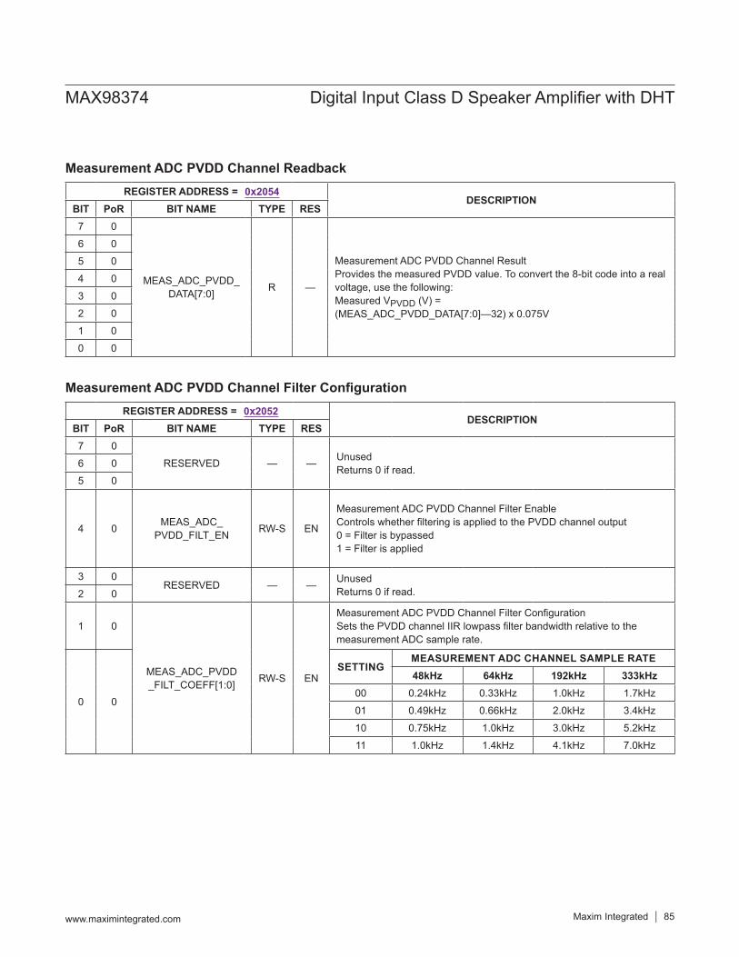
Measurement ADC PVDD Channel Filter Configuration
Measurement ADC PVDD Channel ReadbackREGISTER ADDRESS = 0x2054
DESCRIPTIONBIT PoR BIT NAME TYPE RES7 0
MEAS_ADC_PVDD_DATA[7:0] R —
Measurement ADC PVDD Channel ResultProvides the measured PVDD value. To convert the 8-bit code into a real voltage, use the following: Measured VPVDD (V) = (MEAS_ADC_PVDD_DATA[7:0]—32) x 0.075V
6 05 04 03 02 01 00 0
REGISTER ADDRESS = 0x2052DESCRIPTION
BIT PoR BIT NAME TYPE RES7 0
RESERVED — — Unused Returns 0 if read.6 0
5 0
4 0 MEAS_ADC_PVDD_FILT_EN RW-S EN
Measurement ADC PVDD Channel Filter EnableControls whether filtering is applied to the PVDD channel output0 = Filter is bypassed1 = Filter is applied
3 0RESERVED — — Unused
Returns 0 if read.2 0
1 0
MEAS_ADC_PVDD_FILT_COEFF[1:0] RW-S EN
Measurement ADC PVDD Channel Filter ConfigurationSets the PVDD channel IIR lowpass filter bandwidth relative to the measurement ADC sample rate.
0 0
SETTINGMEASUREMENT ADC CHANNEL SAMPLE RATE48kHz 64kHz 192kHz 333kHz
00 0.24kHz 0.33kHz 1.0kHz 1.7kHz01 0.49kHz 0.66kHz 2.0kHz 3.4kHz10 0.75kHz 1.0kHz 3.0kHz 5.2kHz11 1.0kHz 1.4kHz 4.1kHz 7.0kHz
MAX98374 Digital Input Class D Speaker Amplifier with DHT
www.maximintegrated.com Maxim Integrated 85
Clock MonitorThe device provides an optional clock monitor that is enabled by setting CMON_EN (Device Auto-Restart Configuration) to 1. When enabled, the block monitors the active clock source (BCLK in I2C control/PCM inter-face mode and SWCLK in SoundWire control mode) and automatically places the device into shutdown if a clock source error is detected. This prevents unwanted signals from reaching the speaker path output during a fault con-dition.The clock monitor detects a clock source error if the monitored clock source (BCLK or SWCLK) stops high or low for more than 60μs (typ). The timeout of the clock monitor is determined by an internal oscillator, which has a typical variability of ±10% over the devices operating temperature range.The clock monitor can be programmed to respond to the loss and reapplication of the clock source in two ways. When the CMON_AUTORESTART_EN bit (Device Auto-Restart Configuration) is set to 0 and a clock source error is detected, the clock monitor generates an interrupt (CLKSTOP_*) and places the device into software shut-
down by setting EN to 0. When a valid clock is reapplied, the clock monitor generates an interrupt (CLKSTART_*); however, the device remains in software shutdown until the host sets EN to 1.When the CMON_AUTORESTART_EN bit is set to 1 and a clock source error is detected, the clock monitor gener-ates an interrupt (CLKSTOP_*) and places the device into shutdown internally. When a valid clock is reapplied, the clock monitor generates an interrupt (CLKSTART_*) and the device automatically exits shutdown. The value of EN is not changed in auto restart mode, and remains 1 throughout the process. As a result, when auto restart is enabled, the device does not go through the full power-down/up sequence, and audible glitches may occur.
Clock Monitor in SoundWire Control ModeIf the SoundWire master uses ClockStop events, then the clock monitor should be disabled in SoundWire con-trol mode. In this case, to prevent audible glitches, the SoundWire master should instead place the device into software shutdown directly prior to initiating a ClockStop event.
Measurement ADC PVDD Channel EnableREGISTER ADDRESS = 0x2056
DESCRIPTIONBIT PoR BIT NAME TYPE RES7 0
RESERVED — — Unused Returns 0 if read.
6 05 04 03 02 01 0
0 0 MEAS_ADC_PVDD_EN RW-D —
Measurement ADC PVDD Channel EnableManually enables the measurement ADC PVDD channel.0 = PVDD channel disabled1 = PVDD channel enabled
MAX98374 Digital Input Class D Speaker Amplifier with DHT
www.maximintegrated.com Maxim Integrated 86

Device Auto-Restart ConfigurationREGISTER ADDRESS = 0x20FE DESCRIPTION
BIT PoR BIT NAME TYPE RES7 0
RESERVED — — Unused Returns 0 if read.
6 05 04 0
3 0 OVC_ AUTORESTART_EN RW-S EN
Speaker Amplifier Overcurrent Automatic Restart EnableControls whether or not the speaker amplifier automatically re-enables after an overcurrent fault condition.0 = Overcurrent recovery is in manual mode1 = Overcurrent recovery is in auto mode
2 0 THERM_ AUTORESTART_EN RW-S EN
Thermal Shutdown Automatic Restart EnableControls whether or not the device automatically resumes playback when the die temperature recovers from thermal shutdown. 0 = Thermal shutdown recovery is in manual mode1 = Thermal shutdown recovery is in auto mode
1 0 CMON_ AUTORESTART_EN RW-S EN
Clock Monitor Automatic Restart EnableControls whether or not the device automatically resumes playback when the clock returns after stopping. 0 = Device does not automatically restart when a valid clock is reapplied1 = Device automatically restarts when a valid clock is reapplied
0 0 CMON_EN RW-S EN
Clock Monitor EnableEnable the clock monitor.0 = Clock monitor disabled1 = Clock monitor enabled
MAX98374 Digital Input Class D Speaker Amplifier with DHT
www.maximintegrated.com Maxim Integrated 87

Dynamic Headroom Tracking (DHT)The device features DHT to preserve consistent dynamic range in the presence of a varying supply. DHT maintains consistent volume and listening levels up to a program-mable threshold below full scale (referred to as the rota-tion point or RP). DHT maintains the headroom of the amplifier at signal peaks that occur above the rotation point up to full scale to ensure consistent, smooth com-pression in the presence of supply variations.DHT is enabled with the DHT_EN bit (DHT Enable). When DHT is enabled, the measurement ADC PVDD channel is automatically enabled and routed to the DHT block. The conversion results are used to calculate the amount of compression (if any) that is applied to signal peaks above the configured rotation point.The DHT functionality is configured by several key parameters. The first is the speaker path full-scale gain maximum setting (SPK_GAIN_MAX, Speaker Path Output Level Scaling). This sets the no-load maximum peak output-voltage level (VMPO) that the Class D ampli-fier reproduces with a full-scale (0dBFS) input signal. This level is compared to the current VPVDD level to determine what the available headroom is. The second parameter is the DHT voltage rotation point (VRP). The rotation point is selected with the DHT_VROT_PNT bit (DHT Configuration) and sets the level in dBFS above
which compression is applied to the output signal (when the VPVDD voltage level drops below VMPO). Finally, DHT uses the gain minimum parameter (DHT_SPK_GAIN_MIN, DHT Configuration) to control the maximum compression ratio (VMIN). This parameter enables a second inflection point on the transfer function when the current VPVDD level is below the VMIN setting. In this case, the compression ratio does not increase any fur-ther and signals above the currently available headroom clips instead. Note that if the limiter block is enabled with DHT active, the output-voltage level is limited anytime the input signal to the limiter block exceeds the configured limiter threshold regardless of the DHT configuration and operating point.
DHT Modes of OperationThe DHT has three general modes of operation. The mode of operation depends on the VPVDD level relative to the no-load maximum peak output-voltage level (VMPO) and the selected rotation point (VRP).
MODE 1: VPVDD is greater than VMPOIf VPVDD is greater than VMPO, then there is no action taken by the DHT block. There is sufficient headroom for the amplifier to linearly represent any signal up to and including 0dBFS; the signal transfer function is unaf-fected.
Figure 25. Example of DHT in Mode 1 Operation
VMPO
0-6
CONFIGURED ROTATION POINT
OUTP
UT-V
OLTA
GE LE
VEL (
V P)
INPUT SIGNAL LEVEL (dBFS)
VPVDD > VMPO
VRP
MAX98374 Digital Input Class D Speaker Amplifier with DHT
www.maximintegrated.com Maxim Integrated 88

MODE 2: VPVDD is less than VMPO and greater than VRPDHT operates in mode 2 when VPVDD drops below VMPO but remains above the rotation point (VRP). The transfer function for signals below VRP is exactly as in mode 1. However, signal levels between VRP and full scale (0dBFS) are now subject to the calculated compression ratio.The compression ratios in mode 2 are calculated from the combination of the current VPVDD level, the rotation point (VRP), the SPK_GAIN_MAX (VMPO), and DHT_SPK_GAIN_MIN (VMIN) settings. DHT then applies the calculat-ed ratio for peaks over VRP at the programmed attack and release rates (see the DHT Ballistics section). Figure 26 and Figure 27 illustrate the mode 2 transfer function.
MODE 3a: VPVDD is less than VRP and greater than VMINWhen the rotation point (VRP) is set to a higher value than the current VPVDD level, but VPVDD still exceeds the configured VMIN DHT operates in mode 3a. If VPVDD is less than VRP, then the effective rotation point must now be set by the current VPVDD level. The device automati-cally determines this new rotation point and hard limiting (clipping) is applied to signal peaks exceeding it.The rotation point (VRP) should be selected so that this mode is never used. The rotation point typically should be set to reflect the lowest VPVDD level expected.
Figure 26. Example of DHT in Mode 2 Operation with VRP ≥ VMIN
VMPO
VRP
0-6
PEAK OUTPUT SCALED TO FIT AVAILABLE VPVDD
THE COMPRESSION RATIO IS SCALED TO FIT THE TRANSFER FUNCTION AUTOMATICALLY BETWEEN THE ROTATION POINT AND THEORETICAL PEAK OUTPUT VOLTAGE (AS DETERMINED BY THE MEASURED VPVDD)
DECR
EASI
NG V
PVDD
OUTP
UT-V
OLTA
GE LE
VEL (
V P)
INPUT SIGNAL LEVEL (dBFS)
VRP < VPVDD < VMPO
ROTA
TION
POI
NT
MAX98374 Digital Input Class D Speaker Amplifier with DHT
www.maximintegrated.com Maxim Integrated 89

Figure 27. Example of DHT in Mode 2 Operation with VRP < VMIN
Figure 28. Example of DHT in Mode 3a Operation (Limiter Disabled)
VMPO
0-30
VRP
PEAK OUTPUT SCALED TO FIT AVAILABLE VPVDD
OUTP
UT-V
OLTA
GE LE
VEL (
V P)
INPUT SIGNAL LEVEL (dBFS)
ROTA
TION
POI
NTDE
CREA
SING
VPV
DD
VMIN < VPVDD < VMPO
THE COMPRESSION RATIO IS SCALED TO FIT THE TRANSFER FUNCTION AUTOMATICALLY BETWEEN THE ROTATION POINT AND THEORETICAL PEAK OUTPUT VOLTAGE (AS DETERMINED BY THE MEASURED VPVDD)
VMIN
VMPO
0-6
OUTP
UT-V
OLTA
GE LE
VEL (
V P)
INPUT SIGNAL LEVEL (dBFS)
VRPVMIN < VPVDD < VRP
WHEN VPVDD < VEXP_RP A NEW ROTATION POINT IS AUTOMATICALLY DETERMINED AND INFINITE COMPRESSION IS APPLIED.
ROTA
TION
POI
NT
DECR
EASI
NG V
PVDD
CLIPPING
VMIN
MAX98374 Digital Input Class D Speaker Amplifier with DHT
www.maximintegrated.com Maxim Integrated 90

MODE 3b: VPVDD is less than VMIN and greater than VRPThis mode can only occur if the rotation point (VRP) is set lower than VMIN. In this configuration, if VPVDD is less than VMIN, the DHT cannot compress the signal any further. As VPVDD decreases below VMIN, the compres-sion ratio stays fixed and the output signal starts to clip (Figure 29). This clipping can be eliminated if the limiter is enabled in addition to the DHT (Figure 30).
The transfer function shown in Figure 30 is typically preferable to the transfer function shown in Figure 29. When the DHT and the limiter are used together, it allows for the creation of a second inflection point on the transfer function. This second inflection point reduces the tran-sition from compression to limiting and minimizes the audible impact of signal manipulation by the DHT.
Figure 29. Example of DHT in Mode 3b Operation (Limiter Disabled)
VMPO
0-30
VRP
VRP < VPVDD < VMIN
OUTP
UT-V
OLTA
GE LE
VEL (
V P)
INPUT SIGNAL LEVEL (dBFS)
COMPRESSION CLIPPING
DECR
EASI
NG V
PVDD
VMIN
ROTA
TION
POI
NT
LIMITER DISABLED
MAX98374 Digital Input Class D Speaker Amplifier with DHT
www.maximintegrated.com Maxim Integrated 91

Figure 30. Example of Dynamic Headroom Tracking in Mode 3b Operation (Limiter Enabled)
DHT Enable
THE BEHAVIOR SHOWN IS THE RESULT OF THE DHT
AND THE LIMITER WORKING IN CONCERT
VMPO
0-30
VRP
VRP < VPVDD < VMIN
OUTP
UT V
OLTA
GE LE
VEL
(VP)
INPUT SIGNAL LEVEL (dBFS)
COMPRESSION LIMITING
DECR
EASI
NG V
PVDD
VMIN
ROTA
TION
POI
NT
LIMITER ENABLED
REGISTER ADDRESS = 0x20D4DESCRIPTION
BIT PoR BIT NAME TYPE RES7 0
RESERVED — — Unused Returns 0 if read.
6 05 04 03 02 01 0
0 0 DHT_EN RW-S EN
DHT Enable ControlSelect whether DHT is enabled or disabled.0 = DHT is disabled1 = DHT is enabled
MAX98374 Digital Input Class D Speaker Amplifier with DHT
www.maximintegrated.com Maxim Integrated 92

DHT BallisticsWhen an input signal exceeds the rotation point (VRP), DHT compression activates and attenuates the signal at the programmed attack rate. The DHT attack rate and step size are both configurable (DHT Attack Rate Settings).The instant that a large signal is input to the device, the output tries to reproduce that signal without any attenu-ation from the DHT. Over the total attack time, the DHT applies compression to ensure that the signal fits within the available PVDD voltage. However, if a large enough input signal is applied suddenly, there can be hard clip-ping on the output for a short time. However, after the full attack time has completed, there should be no clipping if sufficient headroom is available. In cases with insufficient headroom, after the attack time has completed, clipping can be prevented by using the limiter with the DHT (see the Limiter section).Observing the output waveform, the amount of attenua-tion applied increases up to when VIN (dBFS) = VPVDD
(dBFS). Once VIN (dBFS) is greater than VPVDD (dBFS), the amount of attenuation observed in the output wave-form appears to decrease. This is a result of the output clipping against the PVDD voltage level. In this case, DHT still takes the same amount of time to apply the full compression as though it had the headroom to reproduce the signal.When compression is active and the input signal falls back down below the rotation point (VRP), DHT releases the applied attenuation at the configured release rate. The DHT release rate and release step size are both configu-rable (DHT Release Rate Settings).When a change in PVDD level triggers the compression algorithm in the DHT block, it has a typical delay of 30µs (until attack or release begins); however, the maximum total latency can approach 60µs. This is caused by a combination of the measurement ADC latency, DSP com-pute time, and clock edge alignment. If a change in audio amplitude is the trigger, the total delay time is approxi-mately 600µs.
DHT ConfigurationREGISTER ADDRESS = 0x20D1
DESCRIPTIONBIT PoR BIT NAME TYPE RES
7 0
DHT_SPK_GAIN_MIN[3:0] RW-S EN
DHT Speaker Gain MinimumSets the speaker gain minimum (VMIN). Values in dB are relative to the baseline speaker path DAC full-scale output level of 3.68dBV.0000: 5.43VP (8dB) 0110: 10.83VP (14dB)0001: 6.09VP (9dB) 0111: 12.15VP (15dB)0010: 6.83VP (10dB) 1000: 13.63VP (16dB)0011: 7.66VP (11dB) 1001: 15.29VP (17dB)0100: 8.60VP (12dB) 1010 -1111: Reserved
0101: 9.65VP (13dB)
6 0
5 0
4 0
3 0
DHT_VROT_PNT[3:0] RW-S EN
DHT Rotation PointSets the DHT rotation point.0000: -0.5dBFS 1000: -10dBFS0001: -1dBFS 1001: -12dBFS0010: -2dBFS 1010: -15dBFS0011: -3dBFS 1011: -18dBFS0100: -4dBFS 1100: -20dBFS0101: -5dBFS 1101: -22dBFS0110: -6dBFS 1110: -25dBFS0111: -8dBFS 1111: -30dBFS
2 0
1 0
0 1
MAX98374 Digital Input Class D Speaker Amplifier with DHT
www.maximintegrated.com Maxim Integrated 93

DHT Headroom CalculationTo establish where VPVDD is relative to VMPO, use the following equation:Equation 1:
PVDD (dB) = 20 log(VPVDD/VMPO)VPVDD is the voltage readback from the measurement ADC PVDD channel, and VMPO is the maximum peak out-put voltage. For example, if VPVDD = 13.63V and VMPO = 13.63V (default), then PVDD (dB) = 0dB (the maximum value for PVDD (dB)). If solving Equation 1 returns a value greater than 0dB, then 0dB should be used for further cal-culations. This is important as the DHT only ever applies attenuation and never applies positive gain.For example, if VPVDD = 9.65V and VMPO = 13.63V (default), then solving Equation 1 yields approximately -3dB. This is the VPVDD level relative to VMPO in dB. To find the expected compressed output voltage, use the following equation:Equation 2:
ATTENUATION (dB) = PVDD (dB) – INPUT (dBFS) x (PVDD (dB)/RP (dBFS))
When PVDD (dB) = 0, the PVDD (dB) and the fraction term drop out, which gives attenuation equal to zero. This makes sense because when PVDD (dB) = 0 there is sufficient headroom to playback any signal input into the device and no compression is needed.As before, assume PVDD (dB) = -3dBFS. Now, if the rotation point (VRP) is set to -10dBFS and the input signal level is set to -5dBFS, equation 2 can be used to find the output signal attenuation:
ATTENUATION (dB) = PVDD (dB) – INPUT (dBFS) x (PVDD (dB)/RP (dBFS))
ATTENUATION (dB) = -3dB – (-5dBFS x -3dB/-10dBFS)ATTENUATION (dB) = -1.5dB
For this example, the total amount of compression applied by DHT is 1.5dB. The output signal level can be found by summing the input signal level to the calculated output attenuation.
OUTPUT (dBFS) = INPUT (dBFS) + ATTENUATION (dB) = -6.5dBFS
Figure 31. DHT Attack Functionality
VMPO
0-10
VEXP_RP
-3 dB = PVDD (dB)
OUTP
UT-V
OLTA
GE LE
VEL (
V P)
INPUT SIGNAL LEVEL (dBFS)
VPVDD = 9.65V
ATTACK
THE ATTACK ARROW DEMONSTRATES THE TRANSISTION FROM AN UNATTENUATED SIGNAL TO THE COMPRESSED SIGNAL THAT OCCURS OVER THE TOTAL ATTACK TIME.
ROTA
TION
POI
NT (R
P)
VPVDD = 13.63V
DECR
EASI
NG V
PVDD
ATTENUATION (dB) = -1.5 dB
-5
INPU
T SI
GNAL
LEVE
L
MAX98374 Digital Input Class D Speaker Amplifier with DHT
www.maximintegrated.com Maxim Integrated 94

DHT Attack Rate Settings
DHT Release Rate Settings
REGISTER ADDRESS = 0x20D2DESCRIPTION
BIT PoR BIT NAME TYPE RES7 0
RESERVED — — Unused Returns 0 if read.6 0
5 0
4 0
DHT_ATK_STEP[1:0] RW-S EN
DHT Attack Step SizeSets the DHT compressor attack step size.00: 0.25dB01: 0.5dB10: 1.0dB11: 2.0dB
3 0
2 0
DHT_ATK_RATE[2:0] RW-S EN
DHT Attack RateSets the DHT compressor attack rate. 000: 17.5μs/step001: 35μs/step010: 70μs/step011: 140μs/step100: 280μs/step101: 560μs/step110: 1120μs/step111: 2240μs/step
1 1
0 0
REGISTER ADDRESS = 0x20D3DESCRIPTION
BIT PoR BIT NAME TYPE RES
7 0
RESERVED — — Unused Returns 0 if read.6 0
5 0
4 0
DHT_RLS_STEP[1:0] RW-S EN
DHT Release Step SizeSets the DHT compressor release step size.00: 0.25dB01: 0.5dB10: 1.0dB11: 2.0dB
3 0
2 0
DHT_RLS_RATE[2:0] RW-S EN
DHT Release RateSets the DHT compressor release rate. 000: 45ms/step001: 225ms/step010: 450ms/step011: 1150ms/step100: 2250ms/step101: 3100ms/step110: 4500ms/step111: 6750ms/step
1 1
0 1
MAX98374 Digital Input Class D Speaker Amplifier with DHT
www.maximintegrated.com Maxim Integrated 95

LimiterThe device features a programmable limiter that is used to compress large near full-scale signals. The limiter func-tions both during normal operation (BDE disabled or inac-tive) and in conjunction with the BDE level configurations. In normal operation with the BDE controller disabled (BDE_EN = 0, Brownout Detection Engine Enable) or inactive (BDE_EN = 1 and BDE_STATE = 0, Brownout Detection Engine Current State), the limiter is enabled when the LIM_EN bit (Limiter Enable) is set to 1. The limiter threshold is manually programmed with the LIM_THRESH bit field, (Limiter Threshold Configuration) and can be con-figured from 0dBFS to -15dBFS in 1 dB steps.
When the BDE is both enabled (BDE_EN = 1) and active (BDE_STATE > 0) the LIM_EN, LIM_THRESH_SEL, and LIM_THRESH settings are ignored. In this state, the limiter threshold is determined solely by the current BDE level. Each BDE level has an individually configured lim-iter threshold setting (set by BDE_Ln_LIM).The limiter attack and release rates are programmable using the LIM_ATK_RATE and LIM_RLS_RATE bit fields respectively (Limiter Attack and Release Rate Configuration). Attenuation is applied when the output signal is higher than the current limiter threshold, and is released once the output signal returns to a level below that threshold. The configured limiter attack and release rates apply to all limiter operating modes.
Figure 32. Example of Limiter Operation with the BDE Inactive
INPUT SIGNAL (dBFS)
OUTP
UT S
IGNA
L (dB
)
LIMITER KNEE = -6dBFS
-6 0-12
SPK_GAIN_MAX = 17dB
SPK_GAIN_MAX = 15dB
SPK_GAIN_MAX = 13dB
PEAK OUTPUT LIMITED TO VMPO-LIMITER
THRESHOLD SETTING (VPVDD ≥ VMPO)
MAX98374 Digital Input Class D Speaker Amplifier with DHT
www.maximintegrated.com Maxim Integrated 96

Limiter Threshold Configuration
Limiter Enable
REGISTER ADDRESS = 0x20E0DESCRIPTION
BIT PoR BIT NAME TYPE RES
7 0 RESERVED — — Unused Returns 0 if read.
6 0
LIM_THRESH[4:0] RW-S EN
Limiter Threshold SettingSelects the limiter threshold setting (dBFS below VMPO).00000: 0dBFS 00001: -1dBFS 00010: -2dBFS … (-1dBFS steps)01110: -14dBFS 01111: -15dBFS 10000 to 11111: Reserved
5 0
4 0
3 0
2 0
1 0RESERVED — — Unused
Returns 0 if read.0 0
0 0 RESERVED — — UnusedReturns 0 if read.
REGISTER ADDRESS = 0x20E2DESCRIPTION
BIT PoR BIT NAME TYPE RES7 0
RESERVED — — Unused Returns 0 if read.
6 05 04 03 02 01 0
0 0 LIM_EN RW-S EN
Limiter Enable ControlSelects whether or not the limiter is enabled when the BDE is inactive.0 = Limiter is disabled when the BDE is inactive1 = Limiter is enabled when the BDE is inactive
MAX98374 Digital Input Class D Speaker Amplifier with DHT
www.maximintegrated.com Maxim Integrated 97

Limiter Attack and Release Rate ConfigurationREGISTER ADDRESS = 0x20E1
DESCRIPTIONBIT PoR BIT NAME TYPE RES
7 0
LIM_ATK_RATE[3:0] RW-S EN
Limiter Attack RateSelects the attack rate for the limiter.0000 = 10µs/dB0001 = 20µs/dB0010 = 40µs/dB0011 = 80µs/dB0100 = 160µs/dB0101 = 320µs/dB0110 = 640µs/dB0111 = 1.28ms/dB1000 = 2.56ms/dB1001 = 5.12ms/dB1010 = 10.24ms/dB1011 = 20.48ms/dB1100 = 40.96ms/dB1101 = 81.92ms/dB1110 = 163.84ms/dB1111 = 327.68ms/dB
6 0
5 0
4 0
3 0
LIM_RLS_RATE[3:0] RW-S EN
Limiter Release RateSelects the release rate for the limiter.0000 = 40µs/dB0001 = 80µs/dB0010 = 160µs/dB0011 = 320µs/dB0100 = 640µs/dB0101 = 1.28ms/dB0110 = 2.56ms/dB0111 = 5.12ms/dB1000 = 10.24ms/dB1001 = 20.48ms/dB1010 = 40.96ms/dB1011 = 81.92ms/dB1100 = 163.84ms/dB1101 = 327.68ms/dB1110 = 655.36ms/dB1111 = 1310.72ms/dB
2 0
1 0
0 0
MAX98374 Digital Input Class D Speaker Amplifier with DHT
www.maximintegrated.com Maxim Integrated 98

Brownout-Detection Engine (BDE)The BDE allows the device to reduce its contribution to the overall system power consumption as VPVDD drops. The BDE can be enabled at any time by setting the BDE_EN bit high (BDE Enable). However, the BDE must not be disabled when it is active (in critical supply levels 1 through 4). The BDE can be disabled safely at any time that it is inactive (see Table 17).The input to the BDE controller comes from the mea-surement ADC PVDD channel. If the measurement ADC PVDD channel is not already active, enabling the BDE automatically enables it. The sample rate and filter set-tings for the measurement ADC determine the speed at which the BDE updates.
BDE State Controller and Level ThresholdsThere are a total of four BDE critical battery levels each with individually programmable thresholds. The thresholds for each level are configured with the BDE_L1_VTHRESH to BDE_L4_VTHRESH bit fields respectively. The BDE state controller monitors the measurement ADC PVDD channel results and automatically makes state changes. As the BDE controller progresses to higher BDE levels (e.g., from Level 2 to Level 3), transitions between states happens instantly. However, when the brownout control-ler progresses back to lower levels (e.g., from Level 2 to Level 1), transition thresholds include programmable hysteresis and are subject to the programmable BDE hold time. The current BDE state can be read-back at any time from the BDE_STATE bit field (BDE Current State).
Figure 33. BDE Block Diagram
Table 17. BDE Operating Levels
SPEAKER DSP DATA PATH
PVDD RESULT FROM MEASUREMENT ADC
BDE CONTROLLER
LIMITER GAIN REDUCTION CLIPPER
CURRENT STATE VPVDD SUPPLY OPERATING RANGEBDE Inactive (Level 0) VPVDD > Critical Battery Level 1Critical Supply Level 1 Critical Battery Level 1 + Hysteresis ≥ VPVDD > Critical Battery Level 2Critical Supply Level 2 Critical Battery Level 2 + Hysteresis ≥ VPVDD > Critical Battery Level 3 Critical Supply Level 3 Critical Battery Level 3 + Hysteresis ≥ VPVDD > Critical Battery Level 4Critical Supply Level 4 Critical Battery Level 4 + Hysteresis ≥ VPVDD
MAX98374 Digital Input Class D Speaker Amplifier with DHT
www.maximintegrated.com Maxim Integrated 99

The programmable hold time and threshold hysteresis behaves as follows (consider BDE inactive as level 0):
In level N, transition to level N+1 when VPVDD falls to less than or equal to the level N+1 threshold.
In level N, transition to level N-1 when VPVDD rises and remains above the level N threshold + hysteresis for the configured BDE hold time.
The VPVDD hysteresis is programmed with the BDE_VTHRESH_HYST bit field (BDE Level Threshold Hysteresis) and can be set to be larger than the distance between two levels. Regardless, the BDE state only transitions one level at a time. As a note of caution, it is possible to program the level of hysteresis so that it is not possible to return to the lower BDE levels (even at a normal PVDD voltage level).
The BDE hold time applies to all ascending BDE level transitions and is configured with the BDE_HLD bit field (BDE Level Hold Time). In addition, BDE Level 4 pro-vides an infinite hold option that is enabled by setting the BDE_L4_INF_HLD bit to 1 (BDE Level 4 Clipper and State Configuration). When infinite hold is enabled, once level 4 becomes the active state, the BDE controller will not transition to a lower level even if the battery voltage level rises above the level 4 threshold (including hyster-esis). While in infinite hold, the BDE controller cannot exit level 4 until the BDE_L4_HLD_RLS bit field (BDE Level 4 Infinite Hold Clear) is written with a logic high or the I2C registers are reset to their PoR states.The BDE controller makes states transition as shown in Figure 34.
Figure 34. BDE Level State Transitions
VPVDD ≤ THRESHOLD 1 VPVDD > (THRESHOLD 1 + HYSTERESIS)
VPVDD > (THRESHOLD 2 + HYSTERESIS)
VPVDD > (THRESHOLD 3 + HYSTERESIS)
VPVDD > (THRESHOLD 4 + HYSTERESIS)
VPVDD ≤ THRESHOLD 2
VPVDD ≤ THRESHOLD 3
VPVDD ≤ THRESHOLD 4
BDE PROTECTIONINACTIVE (LEVEL 0)
LEVEL 1
LEVEL 2
LEVEL 3
LEVEL 4OPTIONAL INFINITE HOLD / MUTE
MAX98374 Digital Input Class D Speaker Amplifier with DHT
www.maximintegrated.com Maxim Integrated 100

BDE Level Configuration OptionsFor a given BDE level, the following options are configu-rable to reduce the overall device current draw:
Programmable Speaker Amplifier Path Gain Programmable Speaker Amplifier Signal Limiter Knee Programmable Speaker Amplifier Clipping Limit
Each of these configuration options are individually configurable for each BDE level. In addition, level 4 also includes an optional digital mute. The BDE level 4 digital mute is a protection feature, and if enabled, mute engages rapidly (without regard to attack time settings) upon entering level 4. When exiting level 4, the digital mute releases according to the configured gain reduction release rate (BDE Gain Reduction Attack/Release Rates). Table 18 is provided as an example case (at the global conditions) as opposed to a definitive use case. The illus-
trative case assumes that the BDE is active, but the DHT block is disabled.
BDE Gain ReductionThe gain reduction block applies smooth digital gain changes to the signal path. The gain reduction is pro-grammable from 0dB to -15dB of attenuation in 0.25dB steps and can be selected individually by BDE level using the BDE_Ln_GAIN bit fields.The attack rate is programmable to either be instan-taneous (no ramp) or over a range from 10µs/dB to 163.84ms/dB using the BDE_GAIN_ATK bit field (BDE Gain Reduction Attack/Release Rates). The release rate is also programmable over a range from 40µs/dB to 1310.73ms/dB using the BDE_GAIN_RLS bit field (BDE Gain Reduction Attack/Release Rates). The selected attack and release rate is common to all BDE levels.
Table 18. Example of BDE Settings
Figure 35. Gain Reduction Profile Example with -6dB Setting
INPUT SIGNAL (dBFS)
OUTP
UT S
IGNA
L (dB
FS)
GAIN REDUCTION = -6dB
-6
-6
-12
0
LEVEL NUMBER VPVDD THRESHOLD LIMITER KNEE GAIN REDUCTION CLIPPER LEVELBDE Inactive N/A 0dBFS 0dBFS 0dBFSBDE Level 1 8.100V -5dBFS 0dBFS 0dBFSBDE Level 2 7.200V -7dBFS 0dBFS 0dBFSBDE Level 3 6.300V -9dBFS -3dBFS -9dBFSBDE Level 4 5.475V N/A Mute N/A
MAX98374 Digital Input Class D Speaker Amplifier with DHT
www.maximintegrated.com Maxim Integrated 101

BDE Limiter FunctionWhen the BDE is enabled (BDE_EN = 1) and active (BDE_STATE > 0), the limiter ignores the LIM_EN and LIM_THRESH settings (Limiter Enable and Limiter Threshold Configuration). In this state, the limiter knee threshold is determined solely by the current BDE level. Each BDE level has an individually configured limiter threshold (set by BDE_Ln_LIM) that is programmable from 0dBFS and -15dBFS in 1dB steps.Input signals that exceed the limiter knee threshold are attenuated, while input signals below the threshold are not. The attack and release rates are programmable, and all BDE levels use the same settings (Limiter Attack and Release Rate Configuration).
BDE Clipper FunctionThe BDE clipper limits the maximum digital output codes to a programmable value. The clipper level range is from 0dBFS to -15dBFS in 0.25dB steps and is configured by level using the BDE_Ln_CLIP bit fields. The BDE clipper level threshold is applied based on the current-signal level relative to full scale at the input to the clipper block.
Therefore, signal gain/level adjustments from blocks pre-ceding the clipper block impacts the configured clipper level threshold (Figure 22). An example of this is the speaker path maximum peak output-voltage scaling configuration (SPK_GAIN_MAX, Speaker Path Output Level Scaling). This control uses a combination of digital and analog gain (Table 16). However, the BDE clipper block is positioned between the digital gain and the analog gain blocks in the signal path. Since the digital gain portion of the selected peak output-voltage setting is located before the clipper block, its set-ting can impact the clipper threshold level. Therefore, it should be accounted for when choosing the clipper level threshold.The BDE clipper changes can be configured with the BDE_CLIP_MODE bit (BDE Clipper Mode) to either be applied to the signal path either immediately or to wait until after a zero cross event. If the signal is DC (or simi-lar) and a zero cross events never occur, then the clipper must be configured to make changes immediately.
Figure 36. Limiter Profile Example with -6dBFS Knee Level
INPUT SIGNAL (dBFS)
OUTP
UT S
IGNA
L (dB
FS)
LIMITER KNEE = -6dBFS
-6
-6
-12
0-12
MAX98374 Digital Input Class D Speaker Amplifier with DHT
www.maximintegrated.com Maxim Integrated 102

Figure 37. Clipper Example with -6dBFS Threshold
BDE Current State
0dBFS
-6dBFS
-6dBFS
0dBFS
CLIP LEVEL
ZERO CROSS
0dBFS
-6dBFS
-6dBFS
0dBFS
IMMEDIATE
OFF -6dBFS
REGISTER ADDRESS = 0x20B6DESCRIPTION
BIT PoR BIT NAME TYPE RES7 0
RESERVED — — Unused Returns 0 if read.
6 05 04 0
3 0
BDE_STATE[3:0] R —
BDE Controller Current StateCurrent level of the BDE controller.0000 = BDE is either disabled or inactive0001 to 0100 = Reserved0101 = Level 10110 = Level 20111 = Level 31000 = Level 41001 to 1111 = Reserved
2 0
1 0
0 0
MAX98374 Digital Input Class D Speaker Amplifier with DHT
www.maximintegrated.com Maxim Integrated 103

BDE Level Hold Time
BDE Enable
BDE Level 1 Threshold
REGISTER ADDRESS = 0x2090DESCRIPTION
BIT PoR BIT NAME TYPE RES7 0
BDE_HLD[7:0] RW-R BDE
BDE Level Hold TimeSets the hold time for each ascending state in the BDE controller.0x00 = 0 ms0x01 = 1 ms0x02 = 2 ms... = (1 ms steps)0xFD = 253 ms0xFE = 254 ms0xFF = 255 ms
6 05 04 03 02 01 00 0
REGISTER ADDRESS = 0x20B5DESCRIPTION
BIT PoR BIT NAME TYPE RES7 0
RESERVED — — Unused Returns 0 if read.
6 05 04 03 02 01 0
0 0 BDE_EN RW-D —
BDE Controller EnableEnables and disables the BDE controller. Do not disable the BDE controller when it is actively protecting the system (in levels 1 to 4).0 = BDE controller disabled1 = BDE controller enabled
REGISTER ADDRESS = 0x2097DESCRIPTION
BIT PoR BIT NAME TYPE RES7 0
BDE_L1_VTHRESH[7:0] RW-R BDE
BDE Level 1 Threshold SettingSets the VPVDD threshold for BDE Level 1. The threshold voltage is calculated with the following formula:
VPVDD Threshold = (BDE_L1_VTHRESH[7:0] - 32) x 0.075V
A value of 0x00 (all zeros) means this level is not used and is entirely bypassed (no hold times).
6 05 04 03 02 01 00 0
MAX98374 Digital Input Class D Speaker Amplifier with DHT
www.maximintegrated.com Maxim Integrated 104

BDE Level 2 Threshold
BDE Level 3 Threshold
REGISTER ADDRESS = 0x2098DESCRIPTION
BIT PoR BIT NAME TYPE RES7 0
BDE_L2_VTHRESH[7:0] RW-R BDE
BDE Level 2 Threshold SettingSets the VPVDD threshold for BDE Level 2. The threshold voltage is calculated with the following formula:
VPVDD threshold = (BDE_L2_VTHRESH[7:0] - 32) x 0.075V
A value of 0x00 (all zeros) means this level is not used and is entirely bypassed (no hold times).
6 05 04 03 02 01 00 0
REGISTER ADDRESS = 0x2099DESCRIPTION
BIT PoR BIT NAME TYPE RES7 0
BDE_L3_VTHRESH[7:0] RW-R BDE
BDE Level 3 Threshold SettingSets the VPVDD threshold for BDE Level 3. The threshold voltage is calculated with the following formula:
VPVDD threshold = (BDE_L3_VTHRESH[7:0] - 32) x 0.075V
A value of 0x00 (all zeros) means this level is not used and is entirely bypassed (no hold times).
6 05 04 03 02 01 00 0
MAX98374 Digital Input Class D Speaker Amplifier with DHT
www.maximintegrated.com Maxim Integrated 105

BDE Level 4 Threshold
BDE Level Threshold Hysteresis
REGISTER ADDRESS = 0x209ADESCRIPTION
BIT PoR BIT NAME TYPE RES7 0
BDE_L4_VTHRESH[7:0] RW-R BDE
BDE Level 4 Threshold Setting
Sets the VPVDD threshold for BDE level 4. The threshold voltage is calculated with the following formula:
VPVDD threshold = (BDE_L4_VTHRESH[7:0] - 32) x 0.075V
A value of 0x00 (all zeros) means this level is not used and is entirely bypassed (no hold times).
6 05 04 03 02 01 00 0
REGISTER ADDRESS = 0x209BDESCRIPTION
BIT PoR BIT NAME TYPE RES7 0
BDE_VTHRESH_HYST[7:0] RW-R BDE
BDE Threshold HysteresisSets the BDE level threshold hysteresis for increasing VPVDD.00000000 = No hysteresis00000001 = 1 LSB of hysteresis00000010 = 2 LSBs of hysteresis... = (1 LSB steps)11111110 = 254 LSBs of hysteresis11111111 = 255 LSBs of hysteresis
6 05 04 03 02 01 00 0
MAX98374 Digital Input Class D Speaker Amplifier with DHT
www.maximintegrated.com Maxim Integrated 106

BDE Gain Reduction Attack/Release RatesREGISTER ADDRESS = 0x2091
DESCRIPTIONBIT PoR BIT NAME TYPE RES
7 0
BDE_GAIN_ATK[3:0] RW-R SFB
BDE Gain Reduction Attack Rate ControlSelects the attack rate for BDE gain reduction.0000 = Instantaneous (step change, no ramp)0001 = 10µs/dB0010 = 20µs/dB0011 = 40µs/dB0100 = 80µs/dB0101 = 160µs/dB0110 = 320µs/dB0111 = 640µs/dB1000 = 1.28ms/dB1001 = 2.56ms/dB1010 = 5.12ms/dB1011 = 10.24ms/dB1100 = 20.48ms/dB1101 = 40.96ms/dB1110 = 81.92ms/dB1111 = 163.84ms/dB
6 0
5 0
4 0
3 0
BDE_GAIN_RLS[3:0] RW-R SFB
BDE Gain Reduction Release Rate ControlSelects the release rate for BDE gain reduction.0000 = 40µs/dB0001 = 80µs/dB0010 = 160µs/dB0011 = 320µs/dB0100 = 640µs/dB0101 = 1.28ms/dB0110 = 2.56ms/dB0111 = 5.12ms/dB1000 = 10.24ms/dB1001 = 20.48ms/dB1010 = 40.96ms/dB1011 = 81.92ms/dB1100 = 163.84ms/dB1101 = 327.68ms/dB1110 = 655.36ms/dB1111 = 1310.72ms/dB
2 0
1 0
0 0
MAX98374 Digital Input Class D Speaker Amplifier with DHT
www.maximintegrated.com Maxim Integrated 107

BDE Clipper Mode
BDE Level 1 Limiter Configuration
REGISTER ADDRESS = 0x2092DESCRIPTION
BIT PoR BIT NAME TYPE RES7 0
RESERVED — — Unused Returns 0 if read.
6 05 04 03 02 01 0
0 0 BDE_CLIP_MODE RW-R SFB
BDE Clipper Level Change ModeControls when the BDE clipper level changes are applied.0 = Clip level changes occur on zero cross event1 = Clip level changes occur as soon as possible
REGISTER ADDRESS = 0x20A8DESCRIPTION
BIT PoR BIT NAME TYPE RES7 0
RESERVED — — Unused Returns 0 if read.
6 05 04 0
3 0
BDE_L1_LIM[3:0] RW-R BDE
BDE Level 1 Limiter ThresholdSets the BDE limiter threshold for Level 1.0 = 0dBFS1 = -1dBFS2 = -2dBFS..... = (-1dBFS steps)14 = -14dBFS15 = -15dBFS
2 0
1 0
0 0
MAX98374 Digital Input Class D Speaker Amplifier with DHT
www.maximintegrated.com Maxim Integrated 108

BDE Level 1 Clipper Configuration
BDE Level 1 Gain Reduction Configuration
REGISTER ADDRESS = 0x20A9DESCRIPTION
BIT PoR BIT NAME TYPE RES7 0
RESERVED — — Unused Returns 0 if read.6 0
5 0
BDE_L1_CLIP[5:0] RW-R BDE
BDE Level 1 Clipper ThresholdSets the threshold at which clipping occurs in BDE level 1. 000000 = 0dBFS000001 = -0.25dBFS000010 = -0.50dBFS000011 = -0.75dBFS.... = (-0.25dBFS steps)111010 = -14.50dBFS111011 = -14.75dBFS111100 = -15.00dBFS111101-111111 = Reserved
4 0
3 0
2 0
1 0
0 0
REGISTER ADDRESS = 0x20AADESCRIPTION
BIT PoR BIT NAME TYPE RES7 0
RESERVED — — Unused Returns 0 if read.6 0
5 0
BDE_L1_GAIN[5:0] RW-R BDE
BDE Level 1 Gain ReductionSets the gain reduction for BDE level 1.000000 = 0dB000001 = -0.25dB000010 = -0.50dB000011 = -0.75dB.... = in -0.25dB steps111010 = -14.50dB111011 = -14.75dB111100 = -15.00dB111101-111111 = Reserved
4 0
3 0
2 0
1 0
0 0
MAX98374 Digital Input Class D Speaker Amplifier with DHT
www.maximintegrated.com Maxim Integrated 109
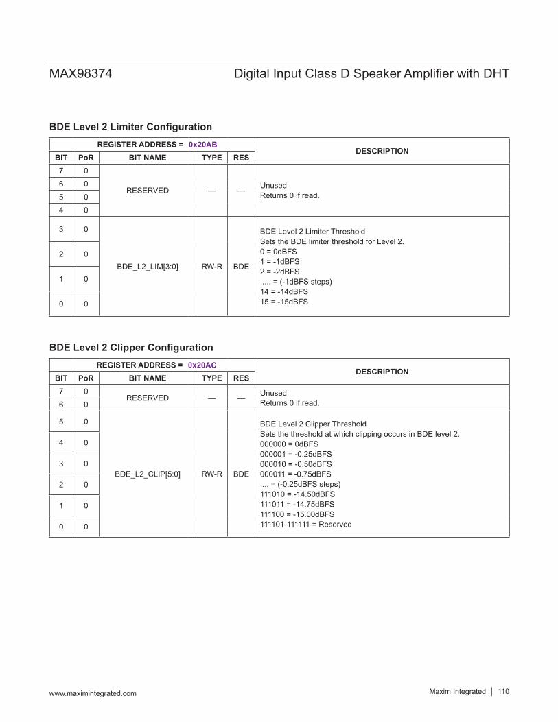
BDE Level 2 Limiter Configuration
BDE Level 2 Clipper Configuration
REGISTER ADDRESS = 0x20ABDESCRIPTION
BIT PoR BIT NAME TYPE RES7 0
RESERVED — — Unused Returns 0 if read.
6 05 04 0
3 0
BDE_L2_LIM[3:0] RW-R BDE
BDE Level 2 Limiter ThresholdSets the BDE limiter threshold for Level 2.0 = 0dBFS1 = -1dBFS2 = -2dBFS..... = (-1dBFS steps)14 = -14dBFS15 = -15dBFS
2 0
1 0
0 0
REGISTER ADDRESS = 0x20ACDESCRIPTION
BIT PoR BIT NAME TYPE RES7 0
RESERVED — — Unused Returns 0 if read.6 0
5 0
BDE_L2_CLIP[5:0] RW-R BDE
BDE Level 2 Clipper ThresholdSets the threshold at which clipping occurs in BDE level 2.000000 = 0dBFS000001 = -0.25dBFS000010 = -0.50dBFS000011 = -0.75dBFS.... = (-0.25dBFS steps)111010 = -14.50dBFS111011 = -14.75dBFS111100 = -15.00dBFS111101-111111 = Reserved
4 0
3 0
2 0
1 0
0 0
MAX98374 Digital Input Class D Speaker Amplifier with DHT
www.maximintegrated.com Maxim Integrated 110

BDE Level 2 Gain Reduction Configuration
BDE Level 3 Limiter Configuration
REGISTER ADDRESS = 0x20ADDESCRIPTION
BIT PoR BIT NAME TYPE RES7 0
RESERVED — — Unused Returns 0 if read.6 0
5 0
BDE_L2_GAIN[5:0] RW-R BDE
BDE Level 2 Gain ReductionSets the gain reduction for BDE level 2.000000 = 0dB000001 = -0.25dB000010 = -0.50dB000011 = -0.75dB.... = in -0.25dB steps111010 = -14.50dB111011 = -14.75dB111100 = -15.00dB111101-111111 = Reserved
4 0
3 0
2 0
1 0
0 0
REGISTER ADDRESS = 0x20AEDESCRIPTION
BIT PoR BIT NAME TYPE RES7 0
RESERVED — — Unused Returns 0 if read.
6 05 04 0
3 0
BDE_L3_LIM[3:0] RW-R BDE
BDE Level 3 Limiter ThresholdSets the BDE limiter threshold for level 3.0 = 0dBFS1 = -1dBFS2 = -2dBFS..... = in -1dBFS steps14 = -14dBFS15 = -15dBFS
2 0
1 0
0 0
MAX98374 Digital Input Class D Speaker Amplifier with DHT
www.maximintegrated.com Maxim Integrated 111

BDE Level 3 Clipper Configuration
BDE Level 3 Gain Reduction Configuration
REGISTER ADDRESS = 0x20AFDESCRIPTION
BIT PoR BIT NAME TYPE RES7 0
RESERVED — — Unused Returns 0 if read.6 0
5 0
BDE_L3_CLIP[5:0] RW-R BDE
BDE Level 3 Clipper ThresholdSets the threshold at which clipping occurs in BDE level 3.000000 = 0dBFS000001 = -0.25dBFS000010 = -0.50dBFS000011 = -0.75dBFS.... = (-0.25dBFS steps)111010 = -14.50dBFS111011 = -14.75dBFS111100 = -15.00dBFS111101-111111 = Reserved
4 0
3 0
2 0
1 0
0 0
REGISTER ADDRESS = 0x20B0DESCRIPTION
BIT PoR BIT NAME TYPE RES7 0
RESERVED — — Unused Returns 0 if read.6 0
5 0
BDE_L3_GAIN[5:0] RW-R BDE
BDE Level 3 Gain ReductionSets the gain reduction for BDE level 3.000000 = 0dB000001 = -0.25dB000010 = -0.50dB000011 = -0.75dB.... = in -0.25dB steps111010 = -14.50dB111011 = -14.75dB111100 = -15.00dB111101-111111 = Reserved
4 0
3 0
2 0
1 0
0 0
MAX98374 Digital Input Class D Speaker Amplifier with DHT
www.maximintegrated.com Maxim Integrated 112

BDE Level 4 Limiter Configuration
BDE Level 4 Clipper and State Configuration
REGISTER ADDRESS = 0x20B1DESCRIPTION
BIT PoR BIT NAME TYPE RES7 0
RESERVED — — Unused Returns 0 if read.
6 05 04 0
3 0
BDE_L4_LIM[3:0] RW-R BDE
BDE Level 4 Limiter ThresholdSets the BDE limiter threshold for level 4.0 = 0dBFS1 = -1dBFS2 = -2dBFS..... = in -1dBFS steps14 = -14dBFS15 = -15dBFS
2 0
1 0
0 0
REGISTER ADDRESS = 0x20B2DESCRIPTION
BIT PoR BIT NAME TYPE RES
7 0 BDE_L4_MUTE RW-R BDE
BDE Level 4 Mute EnableMutes the audio stream when in BDE level 4.0 = Not muted in BDE level 41 = Muted in BDE level 4
6 0 BDE_L4_INF_HLD RW-R- BDE
BDE Controller Level 4 Infinite Hold EnableEnables the BDE level 4 infinite hold feature.0 = Transition from level 4 automatically based on PVDD level 1 = Transition from level 4 only after writing to BDE_L4_HLD_RLS
5 0
BDE_L4_ CLIP[5:0] RW-R BDE
BDE Level 4 Clipper ThresholdSets the threshold at which clipping occurs in BDE level 4. 000000 = 0dBFS000001 = -0.25dBFS000010 = -0.50dBFS000011 = -0.75dBFS.... = (-0.25dBFS steps)111010 = -14.50dBFS111011 = -14.75dBFS111100 = -15.00dBFS111101-111111 = Reserved
4 0
3 0
2 0
1 0
0 0
MAX98374 Digital Input Class D Speaker Amplifier with DHT
www.maximintegrated.com Maxim Integrated 113

BDE Level 4 Gain Reduction Configuration
BDE Level 4 Infinite Hold Clear
REGISTER ADDRESS = 0x20B3DESCRIPTION
BIT PoR BIT NAME TYPE RES7 0
RESERVED — — Unused Returns 0 if read.6 0
5 0
BDE_L4_ GAIN[5:0] RW-R BDE
BDE Level 4 Gain ReductionSets the gain reduction for BDE level 4. 000000 = 0dB000001 = -0.25dB000010 = -0.50dB000011 = -0.75dB.... = in -0.25dB steps111010 = -14.50dB111011 = -14.75dB111100 = -15.00dB111101-111111 = Reserved
4 0
3 0
2 0
1 0
0 0
REGISTER ADDRESS = 0x20B4DESCRIPTION
BIT PoR BIT NAME TYPE RES
7 0 BDE_L4_HLD_RLS W-D —
BDE Controller Level 4 Infinite Hold ReleaseManually releases the BDE controller from level 4 when infinite hold is enabled.0 = Writing zero has no effect1 = Release brownout controller from level 4
6 0
RESERVED — — Unused Returns 0 if read.
5 04 03 02 01 00 0
MAX98374 Digital Input Class D Speaker Amplifier with DHT
www.maximintegrated.com Maxim Integrated 114

Thermal ProtectionWhen the device is active, the measurement ADC thermal channel is automatically enabled and continuously moni-tors die temperature to ensure that it does not exceed the configured thermal thresholds. Interrupt registers are pro-vided so that the device can notify the host when the die temperature crosses the thermal-warning threshold, the thermal-shutdown threshold, or when thermal foldback starts and stops.
Thermal Warning and Shutdown Threshold ConfigurationThe thermal-warning threshold is configured by the THERMWARN_THRESH[5:0] bit field (Thermal-Warning Threshold Configuration) and the thermal-shut-down threshold is configured by the THERMSHDN_THRESH[5:0] bit field (Thermal-Shutdown Threshold Configuration). When the die temperature is decreasing, hysteresis is applied to both thresholds. The temperature hysteresis is configured with the THERM_HYST bit field (Thermal Hysteresis Configuration). The thermal-warning threshold temperature should never be configured higher than the thermal-shutdown threshold temperature minus hysteresis.
Thermal-Warning Threshold Configuration
Thermal-Shutdown Threshold Configuration
REGISTER ADDRESS = 0x2014DESCRIPTION
BIT PoR BIT NAME TYPE RES7 0
RESERVED — — Unused Returns 0 if read.6 0
5 0
THERMWARN_THRESH[5:0]
RW-S EN
Thermal-Warning ThresholdSets the thermal-warning threshold temperature.0x00 to 0x05 = Reserved0x06 = 107.96°C0x07 = 109.24°C0x08 = 110.52°C... = (1.28°C steps)0x25 = 147.64°C0x26 = 148.92°C0x27 to 0x3F = 150.2°C
4 1
3 0
2 0
1 0
0 0
REGISTER ADDRESS = 0x2015DESCRIPTION
BIT PoR BIT NAME TYPE RES7 0
RESERVED — — Unused Returns 0 if read.6 0
5 1
THERMSHDN_THRESH[5:0] RW-S EN
Thermal-Shutdown ThresholdSets the thermal-shutdown threshold temperature.0x00 to 0x05 = Reserved0x06 = 107.96°C0x07 = 109.24°C0x08 = 110.52°C... = (1.28°C steps)0x25 = 147.64°C0x26 = 148.92°C0x27 to 0x3F = 150.2°C
4 0
3 0
2 1
1 1
0 1
MAX98374 Digital Input Class D Speaker Amplifier with DHT
www.maximintegrated.com Maxim Integrated 115

Thermal Shutdown Recovery ConfigurationThe device thermal shutdown recovery behavior is deter-mined by the state of the THERM_AUTORESTART_EN bit (Device Auto-Restart Configuration). When the THERM_AUTORESTART_EN bit is set to 0, the thermal shutdown recovery is in manual mode. In manual mode, when the die temperature exceeds the thermal-shutdown threshold, an interrupt is generated and the amplifier out-put is automatically disabled. Once the die temperature drops below the thermal shutdown and warning thresh-olds, the appropriate interrupts are generated to notify the host. In addition, once the die temperature drops below the thermal warning threshold, the device is placed into software shutdown (EN is set to 0) and remains in that state until the host manually re-enables the device. When the THERM_AUTORESTART_EN bit is set to 1, the thermal shutdown recovery is in automatic mode. In automatic mode, when the die temperature exceeds the thermal-shutdown threshold, an interrupt is generated and the amplifier is automatically disabled. Once the die temperature drops below the thermal-shutdown thresh-old, an interrupt is generated but the amplifier remains disabled. When the temperature drops below the thermal-warning threshold, another interrupt is generated and (unlike manual mode) the amplifier is then automatically re-enabled.
Thermal Foldback ConfigurationThe device features thermal foldback to allow for a smoother audio response to high temperature events. Thermal foldback is enabled by setting the THERMFB_EN bit to 1 (Thermal-Foldback Enable). Once enabled, when the die temperature exceeds the configured thermal-warning threshold (+120°C by default, Thermal-Warning Threshold Configuration), an interrupt is generated and attenuation is applied to the speaker amplifier path. As the die temperature increases, the level of attenuation also increases proportionally up to a maximum level of -12dB (unless the thermal-shutdown threshold is exceeded first). Likewise, as die temperature decreases (including hys-teresis and hold time), the applied attenuation also pro-portionally decreases. The slope of the thermal-foldback attenuation is programmed with the THERMFB_SLOPE bit field (Thermal-Foldback Settings).When thermal foldback is active, the attenuation attack rate (for increasing temperature) is fixed at 10μs/dB. However, the attenuation release rate (for decreasing temperature) is programmable and is configured with the THERMFB_RLS bit field (Thermal-Foldback Settings). For thermal foldback to end, the die temperature must drop below the thermal-warning threshold (including the programmed hysteresis) and remain there for longer than the configured hold time (set with the THERMFB_HOLD bit field, Thermal-Foldback Settings). When this occurs, an interrupt is generated and the attenuation completely releases at the programmed release rate.
Thermal Hysteresis ConfigurationREGISTER ADDRESS = 0x2016
DESCRIPTIONBIT PoR BIT NAME TYPE RES7 0
RESERVED — — Unused Returns 0 if read.
6 05 04 03 02 0
1 0
THERM_HYST[4:0] RW-S EN
Thermal Threshold HysteresisControls the amount of hysteresis applied to the thermal-threshold measurements.00 = 2.56°C01 = 3.84°C10 = 5.12°C11 = 6.40°C
0 0
MAX98374 Digital Input Class D Speaker Amplifier with DHT
www.maximintegrated.com Maxim Integrated 116

Thermal-Foldback Settings
Thermal-Foldback Enable
REGISTER ADDRESS = 0x2017DESCRIPTION
BIT PoR BIT NAME TYPE RES
7 1
THERMFB_HOLD[1:0] RW-S EN
Thermal-Foldback Hold TimeThe thermal-foldback hold time controls how long the device temperature must remain below the configured thermal-threshold hysteresis before thermal-foldback release begins.00: 0ms01: 20ms10: 40ms11: 80ms (default)
6 1
5 0RESERVED — — Unused
Returns 0 if read.4 0
3 0
THERMFB_RLS[1:0] RW-S EN
Thermal-Foldback Release RateThis sets the release rate of the thermal-foldback attenuation.00: 3ms/dB01: 10ms/dB10: 100ms/dB11: 300ms/dB
2 0
1 0
THERMFB_SLOPE[1:0] RW-S EN
Thermal-Foldback Attenuation SlopeThis sets the slope of the thermal-foldback attenuation.00: 0.5dB/°C01: 1.0dB/°C10: 2.0dB/°C11: Reserved
0 0
REGISTER ADDRESS = 0x2018DESCRIPTION
BIT PoR BIT NAME TYPE RES7 0
RESERVED — — Unused Returns 0 if read.
6 05 04 03 02 01 0
7 0 THERMFB_EN RW-S EN
Thermal-Foldback EnableEnables thermal foldback.0: Thermal foldback disabled1: Thermal foldback enabled
MAX98374 Digital Input Class D Speaker Amplifier with DHT
www.maximintegrated.com Maxim Integrated 117

ICC InterfaceThe ICC interface enables multiple MAX98374 devices to be grouped to synchronize device changes from the BDE, limiter, thermal foldback, and DHT blocks. In each group, a single device takes on the role of synchronization master and establishes and aligns the data transfer. Each device in each group transmits one or more channels of data. Each device receives the data of the other grouped devices and reacts accordingly. ICC only operates in I2C control mode, and grouped devices communicate over a single wire ICC bus connected to the bidirectional ICC pin on each device.
ICC Interface Data FormatICC device data is 16 bits in length, and contains both a 4 bit data tag and a 12 bit payload. The data tag is located in the first 4 bits of the data, and decodes to a unique value that indicates the type of data currently being trans-mitted. Table 19 shows the tag decode values for each data source. Data tag values from 0x0 to 0x3 correspond to the four device data types while all other data tag values are reserved. The data payload is located in the next 12 bits, and contains the current device data for the transmitted data type. Trailing padding bits are inserted if the configured channel length exceeds 16 bits.
ICC Interface Device Group AssignmentThe ICC interface allows for devices to be grouped so that adjustments are synchronized. The receive channel enables (ICC_RX_CHn_EN, ICC Receiver Enables 1
and ICC Receiver Enables 2) are used to define groups, and devices receive data from all selected channels. The configured set of receive channels must also include the transmit channel of a given device. Each device in a given group must have identical settings for all ICC receive channel enables. The minimum group size is two devices, however a single group can contain up to four devices.The ICC transmit channel enable bit (ICC_TX_CH_EN, ICC Transmitter Enable) enables the device to output data to an assigned ICC channel. The ICC transmit channel destination bit field (ICC_TX_DEST[3:0], ICC Transmitter Configuration) selects the data channel used for ICC data transmission. For each device, the ICC transmit chan-nel Hi-Z controls (ICC_TX_CHn_HIZ, ICC Transmitter Channel Configuration 1, and ICC Transmitter Channel Configuration 2) should be configured to enable data transmission on the selected destination channel.
ICC Data Transmit and ReceiveThe ICC pin is externally connected to the ICC pins of all other grouped MAX98374 devices to form the ICC bus. Each device uses the ICC bus to provide data feedback to the other grouped devices. The ICC bus operates with the same clock source and data format as the current PCM interface configuration and each grouped device sends a single channel of 16-bit ICC data per frame (Figure 39). Multiple independent groups can share a single ICC bus as long as enough channels are available and no channel assignments overlap across groups.
Figure 38. ICC Data Structure
Figure 39. ICC Bus Data Structure
Table 19. ICC Tag Decode Values
PAYLOAD (12 BITS)TAG (4 BITS)
ICC STATUS DATA STRUCTURE
I2C CONTROL MODEPADDING (0/8/16 BITS)
CHANNEL 3 CHANNEL 0CHANNEL 0ICC
LRCLK
CHANNEL 1 CHANNEL 2 CHANNEL 3
PAYLOAD (12 BITS)TAG (4 BITS)
CHANNEL LENGTH = N BITS
ICC BUS DATA STRUCTURE (4 CHANNEL TDM MODE)
PADDING (N-16 BITS)
TAG VALUE DATA TAG DECODE0x0 Thermal Foldback Data0x1 BDE Data0x2 Limiter Attenuation Data0x3 DHT Data
0x4 to 0xF Reserved
MAX98374 Digital Input Class D Speaker Amplifier with DHT
www.maximintegrated.com Maxim Integrated 118

Zero padding bits occupy any extra channel BCLK cycles if the selected channel length is larger than the 16 bits required for the ICC bus data structure (Figure 39).Device data is transmitted on the ICC bus in a round-robin sequence. Each sequence starts with a data tag of 0 on the first frame, and data is transmitted to each frame in the order of ascending numerical tag values. When the last frame in the sequence is complete (data tag of 3), the next frame restarts the sequence (data tag of 0). Each sequence always contains a frame for each data tag (4 frames per sequence), even if the ICC link for any given data tag is not enabled. Each frame contains one chan-nel of data (for the current data tag) for each device in a given group. Figure 40 illustrates the ICC bus round-robin data sequence.
ICC Interface Group Data SynchronizationAt the end of each frame, each device makes the adjust-ments for each data type that corresponds to either the highest or lowest value reported by all devices within the assigned group. The configuration register bit fields (ICC_x_CONFIG, ICC Data Link Configuration) are used to select whether the highest and lowest value for each data type is used. The configuration settings must match across all devices within an assigned group. This ensures that the adjustments applied by the devices in an assigned group are identical.Once all grouped devices have reported their data, the selected value for that data type is applied to all devices in
the group. For all data types (except BDE data) there is a delay of two frames until a change is made to the devices in a given group.For BDE data, a given device immediately uses its own state if it would move the device to a higher BDE level. The BDE data is still transmitted during the appropriate frame, and can then be applied to the other devices in the assigned group.The delay for ICC data propagating through a configured group is six frames. This is comprised of up to four frames for the data tag to come up in the round-robin rotation, plus the two frame delay for a change to be made.
ICC Interface Link SynchronizationA single device in each group is programmed to be the ICC synchronization master. This device synchronizes the selected data links and aligns the round-robin data transmissions. A single device is configured as the ICC sync master if its selected transmit channel destination (ICC_TX_DEST[3:0]) matches the selected sync mas-ter transmit channel (ICC_SYNC_SLOT[3:0]). All other devices in the assigned group are configured as ICC slave devices. The ICC sync master transmit channel set-ting (ICC_SYNC_SLOT[3:0]) must be identical across all devices in each group, otherwise synchronization is not possible. It is recommended (but not required) that the device with the lowest channel assignment be selected as the ICC sync master.
Figure 40. ICC Bus Round-Robin Data Sequence
DATA
ICC
LRCLK
ICC BUS ROUND-ROBIN DATA SEQUENCE (4 CHANNEL TDM MODE)
2 DATA
DATA
ICC
LRCLK RESTART AT TAG = 0
START AT TAG = 0
2 DATA 2 DATA 3 DATA 3 DATA 3 DATA 3 DATA 0 DATA 0 DATA 0
0 DATA 0 DATA 0 DATA 0 DATA 1 DATA 1 DATA 1 DATA 1 DATA 2 DATA3DATA
PAYLOAD + OPTIONAL PAD
MAX98374 Digital Input Class D Speaker Amplifier with DHT
www.maximintegrated.com Maxim Integrated 119

The ICC synchronization process for a device begins once any data links are enabled (one of more ICC_x_LINK_EN = 1) and the device is not in software shutdown (EN = 1). When this condition is met, a given device attempts ICC synchronization. If ICC synchronization for a given device is not successful before the internal timeout (16383 / fLRCLK) expires, then the synchronization process stops and the device generates an ICC synchronization error interrupt (ICC_SYNC_ERR_*, Device Interrupt Sources). To restart the ICC synchronization process, the host must disable and then re-enable ICC for all timed out devices in an assigned group.When ICC synchronization is enabled for all devices in an assigned group, synchronization locks on and the round-robin data transmissions begin. If ICC synchronization for all devices in each group is already enabled when the data link of the last device is enabled, then the ICC synchronization lock-on takes no more than 16 frames to complete. If the ICC of the last device in an assigned group is enabled by exiting software shutdown (Setting EN = 1), then the ICC synchronization lock time is negli-gible relative to the total device turn-on time.When the ICC synchronization is locked and the round-robin data sequence is active, all devices in a given group must transmit the correct data tags. In any given frame
where an incorrect data tag is present, the grouped devic-es retain and use the data from the last valid frame of that data type. For the duration of the link, if any combination of devices in each group transmits a combined total of three incorrect data tags, then the synchronization lock is broken. In this case, ICC data transmissions stop and an ICC data error interrupt is generated (ICC_DATA_ERR_*, Device Interrupt Sources). For any devices where the ICC interface is still enabled, the last valid data for each data type is retained and the synchronization process restarts. A device fully reverts to its own data only if the ICC inter-face is disabled. For any device, if all data links are disabled (all ICC_x_LINK_EN = 0) or the device enters a shutdown state (such as by setting EN = 0 or due to an event such as thermal shutdown) the transmitted data tags will be incor-rect. This results in the ICC synchronization lock being broken for all devices in the group. The ICC synchroniza-tion lock must be restored before the data transmission sequence can resume.For successful ICC synchronization and for a balanced group response, the host must ensure that the register bits for the following blocks are set to the same values across all devices in an assigned group:
Table 20. Register Settings that Must Match Across an ICC GroupFUNCTIONAL BLOCK MATCHED FUNCTIONALITY
PCM Interface All Clock and Data Format RegistersICC Bus and Data Link Configuration ALL ICC Registers Except for the Device Specific Transmit Channel
BDE Configuration All Registers Must Match if the BDE Data Link is EnabledLimiter Configuration All Register Must Match if the Limiter Data Link is Enabled
Thermal Foldback Configuration All Register Must Match if the Thermal-Foldback Data Link is EnabledDHT Configuration All Register Must Match if the DHT Data Link is Enabled
MAX98374 Digital Input Class D Speaker Amplifier with DHT
www.maximintegrated.com Maxim Integrated 120

ICC Data Link ConfigurationREGISTER ADDRESS = 0x2032
DESCRIPTIONBIT PoR BIT NAME TYPE RES
7 0 ICC_DHT_CONFIG RW-R ICC
ICC DHT Link ConfigurationConfigures the ICC link to react to the highest or lowest DHT value of all devices in the same ICC group0 = Use the lowest DHT attenuation for the DHT link1 = Use the highest DHT attenuation for the DHT link
6 0 ICC_LIM_CONFIG RW-R ICC
ICC Limiter Link ConfigurationConfigures the ICC link to react to the highest or lowest Limiter value of all devices in the same ICC group.0 = Use the lowest limiter attenuation for the limiter link1 = Use the highest limiter attenuation for the limiter link
5 1 ICC_BDE_CONFIG RW-R ICC
ICC BDE Link ConfigurationConfigures the ICC link to react to the highest or lowest BDE value of all devices in the same ICC group.0 = Use the lowest BDE level for the BDE link1 = Use the highest BDE level for the BDE link
4 1 ICC_THERM_CONFIG RW-R ICC
ICC Thermal Link ConfigurationConfigures the ICC link to react to the highest or lowest thermal value of all devices in the same ICC group.0 = Use the lowest temperature result for the thermal link1 = Use the highest temperature result for the thermal link
3 0 ICC_DHT_LINK_EN RW-D —
ICC DHT Link EnableEnables ICC DHT link between devices.0 = ICC DHT link disabled1 = ICC DHT link enabled
2 0 ICC_LIM_LINK_EN RW-D —
ICC Limiter Link EnableEnables ICC LIM link between devices.0 = ICC limiter link disabled1 = ICC limiter link enabled
1 0 ICC_BDE_LINK_EN RW-D —
ICC BDE Link EnableEnables ICC BDE link between devices.0 = ICC BDE link disabled1 = ICC BDE link enabled
0 0 ICC_THERM_LINK_EN RW-D —
ICC Thermal Link EnableEnables ICC thermal link between devices.0 = ICC thermal link disabled1 = ICC thermal link enabled
MAX98374 Digital Input Class D Speaker Amplifier with DHT
www.maximintegrated.com Maxim Integrated 121

ICC Receiver Enables 1REGISTER ADDRESS = 0x202E
DESCRIPTIONBIT PoR BIT NAME TYPE RES
7 0 ICC_RX_CH7_EN RW-R ICCICC Receive Channel 7 Enable0 = ICC receive channel 7 is disabled1 = ICC receive channel 7 is enabled
6 0 ICC_RX_CH6_EN RW-R ICCICC Receive Channel 6 Enable0 = ICC receive channel 6 is disabled1 = ICC receive channel 6 is enabled
5 0 ICC_RX_CH5_EN RW-R ICCICC Receive Channel 5 Enable0 = ICC receive channel 5 is disabled1 = ICC receive channel 5 is enabled
4 0 ICC_RX_CH4_EN RW-R ICCICC Receive Channel 4 Enable0 = ICC receive channel 4 is disabled1 = ICC receive channel 4 is enabled
3 0 ICC_RX_CH3_EN RW-R ICCICC Receive Channel 3 Enable0 = ICC receive channel 3 is disabled1 = ICC receive channel 3 is enabled
2 0 ICC_RX_CH2_EN RW-R ICCICC Receive Channel 2 Enable0 = ICC receive channel 2 is disabled1 = ICC receive channel 2 is enabled
1 0 ICC_RX_CH1_EN RW-R ICCICC Receive Channel 1 Enable0 = ICC receive channel 1 is disabled1 = ICC receive channel 1 is enabled
0 0 ICC_RX_CH0_EN RW-R ICCICC Receive Channel 0 Enable0 = ICC receive channel 0 is disabled1 = ICC receive channel 0 is enabled
MAX98374 Digital Input Class D Speaker Amplifier with DHT
www.maximintegrated.com Maxim Integrated 122

ICC Receiver Enables 2
ICC Transmitter Configuration
REGISTER ADDRESS = 0x202FDESCRIPTION
BIT PoR BIT NAME TYPE RES
7 0 ICC_RX_CH15_EN RW-R ICCICC Receive Channel 15 Enable0 = ICC receive channel 15 is disabled1 = ICC receive channel 15 is enabled
6 0 ICC_RX_CH14_EN RW-R ICCICC Receive Channel 14 Enable0 = ICC receive channel 14 is disabled1 = ICC receive channel 14 is enabled
5 0 ICC_RX_CH13_EN RW-R ICCICC Receive Channel 13 Enable0 = ICC receive channel 13 is disabled1 = ICC receive channel 13 is enabled
4 0 ICC_RX_CH12_EN RW-R ICCICC Receive Channel 12 Enable0 = ICC receive channel 12 is disabled1 = ICC receive channel 12 is enabled
3 0 ICC_RX_CH11_EN RW-R ICCICC Receive Channel 11 Enable0 = ICC receive channel 11 is disabled1 = ICC receive channel 11 is enabled
2 0 ICC_RX_CH10_EN RW-R ICCICC Receive Channel 10 Enable0 = ICC receive channel 10 is disabled1 = ICC receive channel 10 is enabled
1 0 ICC_RX_CH9_EN RW-R ICCICC Receive Channel 9 Enable0 = ICC receive channel 9 is disabled1 = ICC receive channel 9 is enabled
0 0 ICC_RX_CH8_EN RW-R ICCICC Receive Channel 8 Enable0 = ICC receive channel 8 is disabled1 = ICC receive channel 8 is enabled
REGISTER ADDRESS = 0x2034DESCRIPTION
BIT PoR BIT NAME TYPE RES
7 0
ICC_SYNC_SLOT[3:0] RW-R ICC
ICC Synchronization Master Channel SelectionSelects the transmit channel for the ICC synchronization master. 0000 = ICC channel 00001 = ICC channel 1… = …1110 = ICC channel 141111 = ICC channel 15
6 0
5 0
4 0
3 0
ICC_TX_DEST[3:0] RW-R ICC
ICC Data Transmit Channel SelectionSelects the device transmit channel for ICC data.0000 = ICC channel 00001 = ICC channel 1… = …1110 = ICC channel 141111 = ICC channel 15
2 0
1 0
0 0
MAX98374 Digital Input Class D Speaker Amplifier with DHT
www.maximintegrated.com Maxim Integrated 123

ICC Transmitter Channel Configuration 1REGISTER ADDRESS = 0x2030
DESCRIPTIONBIT PoR BIT NAME TYPE RES
7 1 ICC_TX_CH7_HIZ RW-R ICCICC Data Transmit Channel 7 Hi-Z Control0 = Channel 7 drives data (selected as a destination) or zeros (if not)1 = Channel 7 is Hi-Z
6 1 ICC_TX_CH6_HIZ RW-R ICCICC Data Transmit Channel 6 Hi-Z Control0 = Channel 6 drives data (selected as a destination) or zeros (if not)1 = Channel 6 is Hi-Z
5 1 ICC_TX_CH5_HIZ RW-R ICCICC Data Transmit Channel 5 Hi-Z Control0 = Channel 5 drives data (selected as a destination) or zeros (if not)1 = Channel 5 is Hi-Z
4 1 ICC_TX_CH4_HIZ RW-R ICCICC Data Transmit Channel 4 Hi-Z Control0 = Channel 4 drives data (selected as a destination) or zeros (if not)1 = Channel 4 is Hi-Z
3 1 ICC_TX_CH3_HIZ RW-R ICCICC Data Transmit Channel 3 Hi-Z Control0 = Channel 3 drives data (selected as a destination) or zeros (if not)1 = Channel 3 is Hi-Z
2 1 ICC_TX_CH2_HIZ RW-R ICCICC Data Transmit Channel 2 Hi-Z Control0 = Channel 2 drives data (selected as a destination) or zeros (if not)1 = Channel 2 is Hi-Z
1 1 ICC_TX_CH1_HIZ RW-R ICCICC Data Transmit Channel 1 Hi-Z Control0 = Channel 1 drives data (selected as a destination) or zeros (if not)1 = Channel 1 is Hi-Z
0 1 ICC_TX_CH0_HIZ RW-R ICCICC Data Transmit Channel 0 Hi-Z Control0 = Channel 0 drives data (selected as a destination) or zeros (if not)1 = Channel 0 is Hi-Z
MAX98374 Digital Input Class D Speaker Amplifier with DHT
www.maximintegrated.com Maxim Integrated 124

ICC Transmitter Channel Configuration 2
ICC Transmitter Enable
REGISTER ADDRESS = 0x2031DESCRIPTION
BIT PoR BIT NAME TYPE RES
7 1 ICC_TX_CH15_HIZ RW-R ICCICC Data Transmit Channel 15 Hi-Z Control0 = Channel 15 drives data (selected as a destination) or zeros (if not)1 = Channel 15 is Hi-Z
6 1 ICC_TX_CH14_HIZ RW-R ICCICC Data Transmit Channel 14 Hi-Z Control0 = Channel 14 drives data (selected as a destination) or zeros (if not)1 = Channel 14 is Hi-Z
5 1 ICC_TX_CH13_HIZ RW-R ICCICC Data Transmit Channel 13 Hi-Z Control0 = Channel 13 drives data (selected as a destination) or zeros (if not)1 = Channel 13 is Hi-Z
4 1 ICC_TX_CH12_HIZ RW-R ICCICC Data Transmit Channel 12 Hi-Z Control0 = Channel 12 drives data (selected as a destination) or zeros (if not)1 = Channel 12 is Hi-Z
3 1 ICC_TX_CH11_HIZ RW-R ICCICC Data Transmit Channel 11 Hi-Z Control0 = Channel 11 drives data (selected as a destination) or zeros (if not)1 = Channel 11 is Hi-Z
2 1 ICC_TX_CH10_HIZ RW-R ICCICC Data Transmit Channel 10 Hi-Z Control0 = Channel 10 drives data (selected as a destination) or zeros (if not)1 = Channel 10 is Hi-Z
1 1 ICC_TX_CH9_HIZ RW-R ICCICC Data Transmit Channel 9 Hi-Z Control0 = Channel 9 drives data (selected as a destination) or zeros (if not)1 = Channel 9 is Hi-Z
0 1 ICC_TX_CH8_HIZ RW-R ICCICC Data Transmit Channel 8 Hi-Z Control0 = Channel 8 drives data (selected as a destination) or zeros (if not)1 = Channel 8 is Hi-Z
REGISTER ADDRESS = 0x2035DESCRIPTION
BIT PoR BIT NAME TYPE RES7 0
RESERVED — — Unused Returns 0 if read.
6 05 04 03 02 01 0
0 0 ICC_TX_EN RW-R ICC
ICC Transmit ControlSelect whether the ICC pin transmitter is enabled/disabled.0 = ICC transmit disabled1 = ICC transmit enabled
MAX98374 Digital Input Class D Speaker Amplifier with DHT
www.maximintegrated.com Maxim Integrated 125

Layout and GroundingProper layout and grounding are essential for optimum performance. Use at least four PCB layers, and add ther-mal vias to the ground/power plane close to the device to ensure good thermal performance and high-end output power. Good grounding improves audio performance and prevents switching noise from coupling into the audio sig-nal. Ground the power signals and the analog signals of the IC separately at the system ground plane, to prevent switching interference from corrupting sensitive analog signals. Place the recommended supply decoupling capacitors as close as possible to the IC. The PVDD to PGND connection must be kept short and should have minimum trace length and loop area to ensure optimal performance. Use wide, low-resistance output, supply and ground traces. As load impedance decreases, the current drawn from the device outputs increase. At higher current, the resistance of the output traces decreases the power delivered to the load. For example, if 2W is delivered from the speaker output to a 4Ω load through a
100mΩ trace, 49mW is consumed in the trace. If power is delivered through a 10mΩ trace, only 5mW is consumed in the trace. Wide output, supply, and ground traces also improve the power dissipation of the device. The device is inherently designed for excellent RF immunity. For best performance, add ground fills around all signal traces on the top and bottom PCB planes. It is advisable to follow the layout of the MAX98374 EV kit as closely as possible in the application. Thermal and performance measure-ments shown in this data sheet were measured with a 6-layer board with 2 signal layers and 4 ground layers. As a result, the EV kit performance is likely better than what can be achieved with a JEDEC standard board.
WLP Applications InformationFor the latest application details on WLP construction, dimensions, tape carrier information, PCB techniques, bump-pad layout, and recommended reflow temperature profile, as well as the latest information on reliability testing results, refer to the Application Note 1891: Wafer-Level Packaging (WLP) and its Applications.
Table 21. Recommended External Components
Table 22. Unused Connections
See the Typical Application Circuit for component placement.
BUMP VALUE SIZE VOLTAGE RATING (V) DIELECTRICPVDD 10µF 0603 25 X5RPVDD 10µF 0603 25 X5RPVDD 0.1µF 0402 25 X5RPVDD 0.1µF 0402 25 X5RPVDD 220µF — 35 Alum-Elec
VREFC 10µF+30Ω 0201 12 X5RDVDD 1µF 0201 6.3 X5R
WLP FCQFN NAME CONNECTIONE1 20 I.C. Connect to DVDDA3 10 IRQ Leave unconnected if unusedD5 3 DOUT Leave unconnected if unusedE4 2 ICC Connect to DGND if unusedB4 7 LRCLK Connect to DGND if unused
MAX98374 Digital Input Class D Speaker Amplifier with DHT
www.maximintegrated.com Maxim Integrated 126

Typical Application Circuit
OUTN
OUTP
OUTPSNS
OUTNSNS
PVDDDVDDVREFC
ICC
IRQ
SCL
SDA
RESET
ADDR
PGNDDGNDAGND
MAX98374
LRCLK
BCLK / SWCLK
DOUT
DIN / SWDATA
1.5kΩ 1µF
1.71V to 1.89V
0.1µF 0.1µF 10µF 10µF 220µF
5.5V to 16V
10µFSERIAL
CONTROL INTERFACE
INTERCHIPCOM. BUS
PCM INTERFACE
OR
SOUNDWIRE COMPATIBLE INTERFACE
HARDWARE RESET
I.C.
30Ω
MAX98374 Digital Input Class D Speaker Amplifier with DHT
www.maximintegrated.com Maxim Integrated 127

Revision Identification NumberThe device provides a register containing the device revision identification number. The revision identification
number reflects the current physical hardware version and is updated with any hardware revision (Device Revision Identification Number).
+Denotes a lead(Pb) free/ROHS compliant package.T = Tape and reel.
Device Revision Identification Number
Package InformationFor the latest package outline information and land patterns (footprints), go to www.maximintegrated.com/packages. Note that a “+”, “#”, or “-” in the package code indicates RoHS status only. Package drawings may show a different suffix character, but the drawing pertains to the package regardless of RoHS status.
Chip InformationPROCESS: CMOS
Ordering Information
REGISTER ADDRESS = 0x21FFDESCRIPTION
BIT PoR BIT NAME TYPE RES7 0
REV_ID[7:0] R — Device Revision Identification NumberRevision of the device. Updated at every device revision.
6 15 04 03 02 01 10 1
PART NUMBER TEMP RANGE PIN-PACKAGEMAX98374EWA+T -40°C to +85°C 25 WLPMAX98374EWA+ -40°C to +85°C 25 WLPMAX98374EFF+T -40°C to +85°C 22 FCQFNMAX98374EFF+ -40°C to +85°C 22 FCQFN PACKAGE
TYPEPACKAGE
CODEOUTLINE
NO.LAND
PATTERN NO.
25 WLP W252C2-2 21-100162Refer to:
Application Note 1891
22 FCQFN F223A3F+1 21-100223 90-100080
MAX98374 Digital Input Class D Speaker Amplifier with DHT
www.maximintegrated.com Maxim Integrated 128

Revision HistoryREVISIONNUMBER
REVISIONDATE DESCRIPTION PAGES
CHANGED
0 3/18 Initial release —
Maxim Integrated cannot assume responsibility for use of any circuitry other than circuitry entirely embodied in a Maxim Integrated product. No circuit patent licenses are implied. Maxim Integrated reserves the right to change the circuitry and specifications without notice at any time. The parametric values (min and max limits) shown in the Electrical Characteristics table are guaranteed. Other parametric values quoted in this data sheet are provided for guidance.
Maxim Integrated and the Maxim Integrated logo are trademarks of Maxim Integrated Products, Inc.
MAX98374 Digital Input Class D Speaker Amplifier with DHT
© 2018 Maxim Integrated Products, Inc. 129
For pricing, delivery, and ordering information, please contact Maxim Direct at 1-888-629-4642, or visit Maxim Integrated’s website at www.maximintegrated.com.


![Integrated AV Amplifier - pdf.crse.compdf.crse.com/manuals/3856168111.pdf · 6EN Getting Started Hookups Front speakers Front speaker (R) Front speaker (L) Amplifier} ] FRONT SPEAKERS](https://img.dokumen.tips/doc/110x75/5b15a6767f8b9a332f8d45d5/integrated-av-amplifier-pdfcrse-6en-getting-started-hookups-front-speakers.jpg)