Embed Size (px)
Citation preview
General DescriptionThe MAX77813 is a high-efficiency step-up/step-down (buck-boost) converter targeted for single-cell Li+/Li-ion battery powered applications. The device maintains a regulated output voltage from 2.6V to 5.14V across an input voltage range of 2.3V to 5.5V. The device supports up to 2A of output current in boost mode and up to 3A in buck mode. The device seamlessly transitions between buck and boost modes. A unique control algorithm allows high-efficiency, outstanding load, and line transient response. Dedicated enable and power-OK pins allow simple hard-ware control. An I2C serial interface is optionally used for dynamic voltage scaling, system power optimization, and fault read-back. The device supports two inductor current limit options selected by the ILIM pin. The MAX77813 is available in a 20-bump, 1.83mm x 2.13mm wafer-level package (WLP).
Applications Single-Cell Li+/Li-ion Battery Powered Devices Handheld Scanners, Mobile Payment Terminals,
Security Cameras AR/VR Headsets
Features and Benefits VIN Range: 2.30V to 5.5V VOUT Range: 2.60V to 5.14V
(I2C Programmable in 20mV Steps) Up to 2A Output Current in Boost Mode
(VIN = 3.0V, VOUT = 3.4V, ILIM = High) Up to 3A Output Current in Buck Mode (ILIM = High) Up to 97% Peak Efficiency SKIP Mode for Optimal Light Load Efficiency 55µA (Typ) Low Quiescent Current 3.4MHz High Speed I2C Serial Interface Input Current Limit Selection Pin Power-OK Output 2.5MHz Switching Frequency Protection Features
• Soft-Start• Thermal Shutdown• Overvoltage Protection• Overcurrent Protection
1.827mm x 2.127mm, 20-Bump WLP
Ordering Information appears at end of data sheet.
19-8238; Rev 2; 3/19
MAX77813 5.5V Input, 2A, High-Efficiency Buck-Boost Converter
Typical Application Circuit
1μH
10μF
LX1
VSYS
SDA
LX2
IN OUT
OUTS
SCL
PGND
VIO
ENABLE EN
1μF
DC INPUT2.3V TO 5.5V
POWER-OK
47μF
POK
ILIM
SERIAL HOST
MAX77813
CURRENT LIMIT SELECT
VOUT2.6V TO 5.14V2A (BOOST MODE)3A (BUCK MODE)
HIGH-EFFICIENCY BUCK-BOOST CONVERTER WITH OPTIONAL I2C CONTROL IN TINY 20-BUMP WLP
500mV/div
20mV/div
100µs/div
BOOST TO BUCK LINE TRANSIENT RESPONSE
VIN
IOUT = 1.5AVOUT = 3.3V
BOOSTMODE
BOOSTMODE
BUCK MODE
VOUT
3.4V
2.9V
Click here for production status of specific part numbers.
SYS, VIO to GND .................................................-0.3V to +6.0VIN, OUT to PGND .................................................-0.3V to +6.0VPGND to GND ......................................................-0.3V to +0.3VSCL, SDA to GND ..................................... -0.3V to (VIO + 0.3V)EN, ILIM, POK to GND........................... -0.3V to (VSYS + 0.3V)FB to GND .............................................. -0.3V to (VOUT + 0.3V)LX1 to PGND..............................................-0.3V to (VIN + 0.3V)
LX2 to PGND.......................................... -0.3V to (VOUT + 0.3V)LX1/LX2 Continuous RMS Current (Note 1) ........................3.2AOperating Junction Temperature Range .......... -40°C to +125°CJunction Temperature ......................................................+150°CStorage Temperature Range ............................ -65°C to +150°CSoldering Temperature (Reflow) ......................................+260°C
WLPPackage Code W201F2+1
Outline Number 21-0771
Land Pattern Number Refer to Application Note 1891
Thermal Resistance, Four-Layer Board:
Junction to Ambient Thermal Resistance (θJA) 55.49°C/W
MAX77813 5.5V Input, 2A, High-Efficiency Buck-Boost Converter
www.maximintegrated.com Maxim Integrated 2
Note 1: LX1 and LX2 nodes have internal clamp diodes to PGNDBB and INBB. Applications that forward bias to these diodes should ensure that the total power loss does not exceed the power dissipation limit of the IC package.
Absolute Maximum Ratings
Stresses beyond those listed under “Absolute Maximum Ratings” may cause permanent damage to the device. These are stress ratings only, and functional operation of the device at these or any other conditions beyond those indicated in the operational sections of the specifications is not implied. Exposure to absolute maximum rating conditions for extended periods may affect device reliability.
Package Information
Package thermal resistances were obtained using the method described in JEDEC specification JESD51-7, using a four-layer board. For detailed information on package thermal considerations, refer to www.maximintegrated.com/thermal-tutorial.
For the latest package outline information and land patterns (footprints), go to www.maximintegrated.com/packages. Note that a “+”, “#”, or “-” in the package code indicates RoHS status only. Package drawings may show a different suffix character, but the drawing pertains to the package regardless of RoHS status.

(VSYS = VIN = +3.8V, VOUTS = VOUT = +3.3V, TJ = -40°C to +125°C, typical values are at TA ≈ TJ = +25°C, unless otherwise noted.) (Note 4)
PARAMETER SYMBOL CONDITIONS MIN TYP MAX UNITSGENERALInput Voltage Range VIN 2.30 5.50 V
Shutdown Supply Current ISHDN_25C EN = low, TJ = +25°C 0.1
µAISHDN_125C EN = low, TJ = +125°C 1
Input Supply CurrentIQ_SKIP
SKIP mode, no switching,TJ = -40° to +85°C 55 70 µA
IQ_PWM FPWM mode, no load 6 mAActive Discharge Resistance RDISCHG 100 ΩThermal Shutdown Threshold TSHDN Rising, +20°C hysteresis +165 °CH-BRIDGEOutput Voltage Range VOUT I2C programmable (20mV Step) 2.60 5.14 V
Output Voltage AccuracyVOUT_ACC1
FPWM mode, VOUT[6:0] = 0x28, no load, TJ = +25°C -1.0 +1.0
%VOUT_ACC2
SKIP mode, VOUT[6:0] = 0x28,no load, TJ = +25°C -1.0 +4.5
Line Regulation VIN = 2.63V to 5.5V 0.200 %/VLoad Regulation (Note 5) 0.125 %/A
Line Transient Response VOS1VUS1
IOUT = 1.0A, VIN changes from 3.4V to 2.9V in 25µs (20mV/µs),L = 1µH, COUT_NOM = 47µF (Note 5)
50 mV
Load Transient Response VOS2VUS2
VIN = 3.4V, IOUT changes from 10mA to 1.5A in 15µs, L = 1µH, COUT_NOM = 47µF (Note 5)
50 mV
Output Voltage Ramp-Up Slew Rate
BB_RU_SR = 0 20mV/µs
BB_RU_SR = 1 40
Output Voltage Ramp-Down Slew Rate
BB_RD_SR = 0 5mV/µs
BB_RD_SR = 1 10Typical Condition Efficiency ηTYP IOUT = 100mA (Note 5) 95 %Peak Efficiency ηPK (Note 5) 97 %
LX1/2 Current Limit ILIM_LXILIM = high 3.70 4.50 5.70
AILIM = low 1.2 1.80 2.65
High-Side PMOS ON Resistance RDSON(PMOS) ILX = 100mA per switch 40 mΩ
Low-Side NMOS ON Resistance RDSON(NMOS) ILX = 100mA per switch 55 mΩ
Switching Frequency fSW PWM mode, TJ = +25°C 2.25 2.50 2.75 MHz
MAX77813 5.5V Input, 2A, High-Efficiency Buck-Boost Converter
www.maximintegrated.com Maxim Integrated 3
Buck-Boost Electrical Characteristics
(VSYS = VIN = +3.8V, VOUTS = VOUT = +3.3V, TJ = -40°C to +125°C, typical values are at TA ≈ TJ = +25°C, unless otherwise noted.) (Note 4)
Note 2: Limits are 100% production tested at TJ = +25°C. The device is tested under pulsed load conditions such that TJ ≈ TA. Limits over the operating temperature range are guaranteed through correlation using statistical quality control methods.
Note 3: Guaranteed by design. Not production tested.
PARAMETER SYMBOL CONDITIONS MIN TYP MAX UNITS
Turn-On Delay Time tON_DLYFrom EN asserting to LX switching with bias ON 100 µs
Soft-Start Timer tSSIOUT = 10mA, ILIM = high 120
µsIOUT = 10mA, ILIM = low 800
Minimum Effective Output Capacitance CEFF(MIN) 0A < IOUT < 2000mA 16 µF
LX1, LX2 Leakage CurrentILK_25C
VLX1/2 = 0V or 5.5V, VOUT = 5.5V, VSYS = VIN = 5.5V, TJ = +25°C 0.1 1
µAILK_125C
VLX1/2 = 0V or 5.5V, VOUT = 5.5V, VSYS = VIN = 5.5V, TJ = +125°C 0.2
POWER-OK COMPARATOR
Output POK Trip LevelRising threshold 80
%Falling threshold 75
VSYS UNDERVOLTAGE LOCKOUT
VSYS Undervoltage Lockout Threshold
VUVLO_R VSYS rising 2.375 2.50 2.625V
VUVLO_F VSYS falling 2.05
LOGIC AND CONTROL INPUTSInput Low Level VIL EN, ILIM, VSYS = 3.8V, TJ = +125°C 0.4 VInput High Level VIH EN, ILIM, VSYS = 3.8V, TJ = -40°C 1.2 VPOK Output Low Voltage VOL ISINK = 1mA 0.4 V
POK Output High LeakageIOZH_25C TJ = +25°C -1 +1
µAIOZH_125C TJ = +125°C 0.1
INTERNAL PULLDOWN RESISTANCEEN RPD Pulldown resistance to GND 400 800 1600 kΩ
MAX77813 5.5V Input, 2A, High-Efficiency Buck-Boost Converter
www.maximintegrated.com Maxim Integrated 4
Buck-Boost Electrical Characteristics (continued)
(VSYS = 3.8V, VVIO = 1.8V, TJ = -40°C to +125°C, typical values are at TA ≈ TJ = +25°C, unless otherwise noted.) (Note 4)
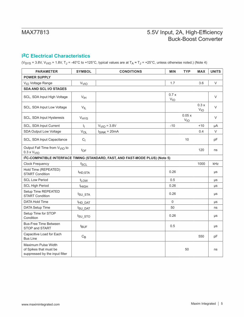
PARAMETER SYMBOL CONDITIONS MIN TYP MAX UNITSPOWER SUPPLYVIO Voltage Range VVIO 1.7 3.6 VSDA AND SCL I/O STAGES
SCL, SDA Input High Voltage VIH0.7 x VIO
V
SCL, SDA Input Low Voltage VIL0.3 x VIO
V
SCL, SDA Input Hysteresis VHYS0.05 x
VIOV
SCL, SDA Input Current II VVIO = 3.8V -10 +10 µASDA Output Low Voltage VOL ISINK = 20mA 0.4 V
SCL, SDA Input Capacitance CI 10 pF
Output Fall Time from VVIO to 0.3 x VVIO
tOF 120 ns
I2C-COMPATIBLE INTERFACE TIMING (STANDARD, FAST, AND FAST-MODE PLUS) (Note 5)Clock Frequency fSCL 1000 kHz
Hold Time (REPEATED) START Condition tHD;STA 0.26 µs
SCL Low Period tLOW 0.5 µsSCL High Period tHIGH 0.26 µs
Setup Time REPEATED START Condition tSU_STA 0.26 µs
DATA Hold Time tHD_DAT 0 µsDATA Setup Time tSU_DAT 50 ns
Setup Time for STOP Condition tSU_STO 0.26 µs
Bus-Free Time Between STOP and START tBUF 0.5 µs
Capacitive Load for Each Bus Line CB 550 pF
Maximum Pulse Width of Spikes that must be suppressed by the input filter
50 ns
MAX77813 5.5V Input, 2A, High-Efficiency Buck-Boost Converter
www.maximintegrated.com Maxim Integrated 5
I2C Electrical Characteristics
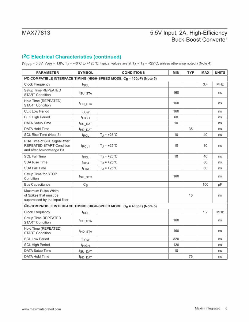
(VSYS = 3.8V, VVIO = 1.8V, TJ = -40°C to +125°C, typical values are at TA ≈ TJ = +25°C, unless otherwise noted.) (Note 4)
PARAMETER SYMBOL CONDITIONS MIN TYP MAX UNITSI2C-COMPATIBLE INTERFACE TIMING (HIGH-SPEED MODE, CB = 100pF) (Note 5)Clock Frequency fSCL 3.4 MHz
Setup Time REPEATED START Condition tSU_STA 160 ns
Hold Time (REPEATED) START Condition tHD_STA 160 ns
CLK Low Period tLOW 160 nsCLK High Period tHIGH 60 nsDATA Setup Time tSU_DAT 10 nsDATA Hold Time tHD_DAT 35 nsSCL Rise Time (Note 3) tRCL TJ = +25°C 10 40 ns
Rise Time of SCL Signal after REPEATED START Condition and after Acknowledge Bit
tRCL1 TJ = +25°C 10 80 ns
SCL Fall Time tFCL TJ = +25°C 10 40 nsSDA Rise Time tRDA TJ = +25°C 80 nsSDA Fall Time tFDA TJ = +25°C 80 ns
Setup Time for STOP Condition tSU_STO 160 ns
Bus Capacitance CB 100 pF
Maximum Pulse Width of Spikes that must be suppressed by the input filter
10 ns
I2C-COMPATIBLE INTERFACE TIMING (HIGH-SPEED MODE, CB = 400pF) (Note 5)Clock Frequency fSCL 1.7 MHz
Setup Time REPEATED START Condition tSU_STA 160 ns
Hold Time (REPEATED) START Condition tHD_STA 160 ns
SCL Low Period tLOW 320 nsSCL High Period tHIGH 120 nsDATA Setup Time tSU_DAT 10 nsDATA Hold Time tHD_DAT 75 ns
MAX77813 5.5V Input, 2A, High-Efficiency Buck-Boost Converter
www.maximintegrated.com Maxim Integrated 6
I2C Electrical Characteristics (continued)

Note 4: Limits are 100% production tested at TJ = +25°C. The device is tested under pulsed load conditions such that TJ ≈ TA. Limits over the operating temperature range are guaranteed through correlation using statistical quality control methods.
Note 5: Guaranteed by design. Not production tested.
(VSYS = 3.8V, VVIO = 1.8V, TJ = -40°C to +125°C, typical values are at TA ≈ TJ = +25°C, unless otherwise noted.) (Note 4)
PARAMETER SYMBOL CONDITIONS MIN TYP MAX UNITSSCL Rise Time tRCL TJ = +25°C 20 80 ns
Rise Time of SCL Signal after REPEATED START Condition and after Acknowledge Bit
tRCL1 TJ = +25°C 20 160 ns
SCL Fall Time tFCL TJ = +25°C 20 80 nsSDA Rise Time tRDA TJ = +25°C 160 nsSDA Fall Time tFDA TJ = +25°C 160 ns
Setup Time for STOP Condition tSU_STO 160 ns
Bus Capacitance CB 400 pF
Maximum Pulse Width of Spikes that Must be Suppressed by the Input Filter
tSP 10 ns
MAX77813 5.5V Input, 2A, High-Efficiency Buck-Boost Converter
www.maximintegrated.com Maxim Integrated 7
I2C Electrical Characteristics (continued)

(VSYS = 3.8V, VOUT = 3.3V, IOUT = 0A, FPWM = 0, TA = +25°C, unless otherwise noted.)
Maxim Integrated 8www.maximintegrated.com
MAX77813 5.5V Input, 2A, High-Efficiency Buck-Boost Converter
Typical Operating Characteristics
0
10
20
30
40
50
60
70
80
90
100
0.001 0.01 0.1 1
EFFIC
IENC
Y (%
)
LOAD (A)
VIN = 3VVIN = 3.3VVIN = 3.8VVIN = 4.5V
VIN = 3.8V (FPWM = 1)
EFFICIENCY vs. LOAD 3.3V OUTPUT
toc04
30
35
40
45
50
55
60
65
70
2 3 4 5 6
QUIE
SCEN
T CU
RREN
T (µ
A)
SUPPLY VOLTAGE (V)
VOUT = 2.8VVOUT = 3.3VVOUT = 5V
QUIESCENT CURRENT vs.SUPPLY VOLTAGE
toc01
3.29
3.30
3.31
3.32
3.33
3.34
3.35
3.36
3.37
3.38
3.39
0.0 0.5 1.0 1.5 2.0
OUTP
UT V
OLTA
GE (V
)
LOAD (A)
VIN = 3VVIN = 3.3VVIN = 3.8VVIN = 4.5V
LOAD REGULATION 3.3V OUTPUT
toc07
-0.5
0.0
0.5
1.0
1.5
2.0
2 3 4 5 6
SHUT
DOW
N CU
RREN
T (µ
A)
SUPPLY VOLTAGE (V)
TA = +25°C
TA = +85°C
TA = -40°C
SHUTDOWN CURRENT vs.SUPPLY VOLTAGE
toc02
4.96
4.98
5.00
5.02
5.04
5.06
5.08
5.10
5.12
5.14
5.16
0.0 0.5 1.0 1.5 2.0
OUTP
UT V
OLTA
GE (V
)
LOAD (A)
VIN = 3VVIN = 3.8VVIN = 4.5V
LOAD REGULATION 5V OUTPUT
toc08
0
10
20
30
40
50
60
70
80
90
100
0.001 0.01 0.1 1
EFFIC
IENC
Y (%
)
LOAD (A)
VIN = 3VVIN = 3.8VVIN = 4.5V
VIN = 3.8V (FPWM = 1)
EFFICIENCY vs. LOAD 2.8V OUTPUT
toc03
2.74
2.75
2.76
2.77
2.78
2.79
2.80
2.5 3.5 4.5 5.5
OUTP
UT V
OLTA
GE (V
)
SUPPLY VOLTAGE (V)
IOUT = 500mAIOUT = 1AIOUT = 2A
LINE REGULATION 2.8V OUTPUT
toc09
0
10
20
30
40
50
60
70
80
90
100
0.001 0.01 0.1 1
EFFIC
IENC
Y (%
)
LOAD (A)
VIN = 3VVIN = 3.8VVIN = 4.5V
VIN = 3.8V (FPWM = 1)
EFFICIENCY vs. LOAD 5V OUTPUT
toc05
2.77
2.78
2.79
2.80
2.81
2.82
2.83
2.84
2.85
0.0 0.5 1.0 1.5 2.0
OUTP
UT V
OLTA
GE (V
)
LOAD (A)
VIN = 3VVIN = 3.8VVIN = 4.5V
LOAD REGULATION 2.8V OUTPUT
toc06

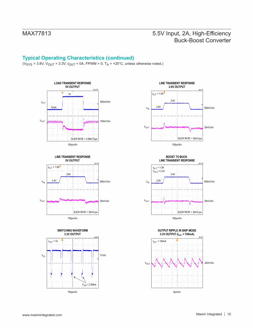
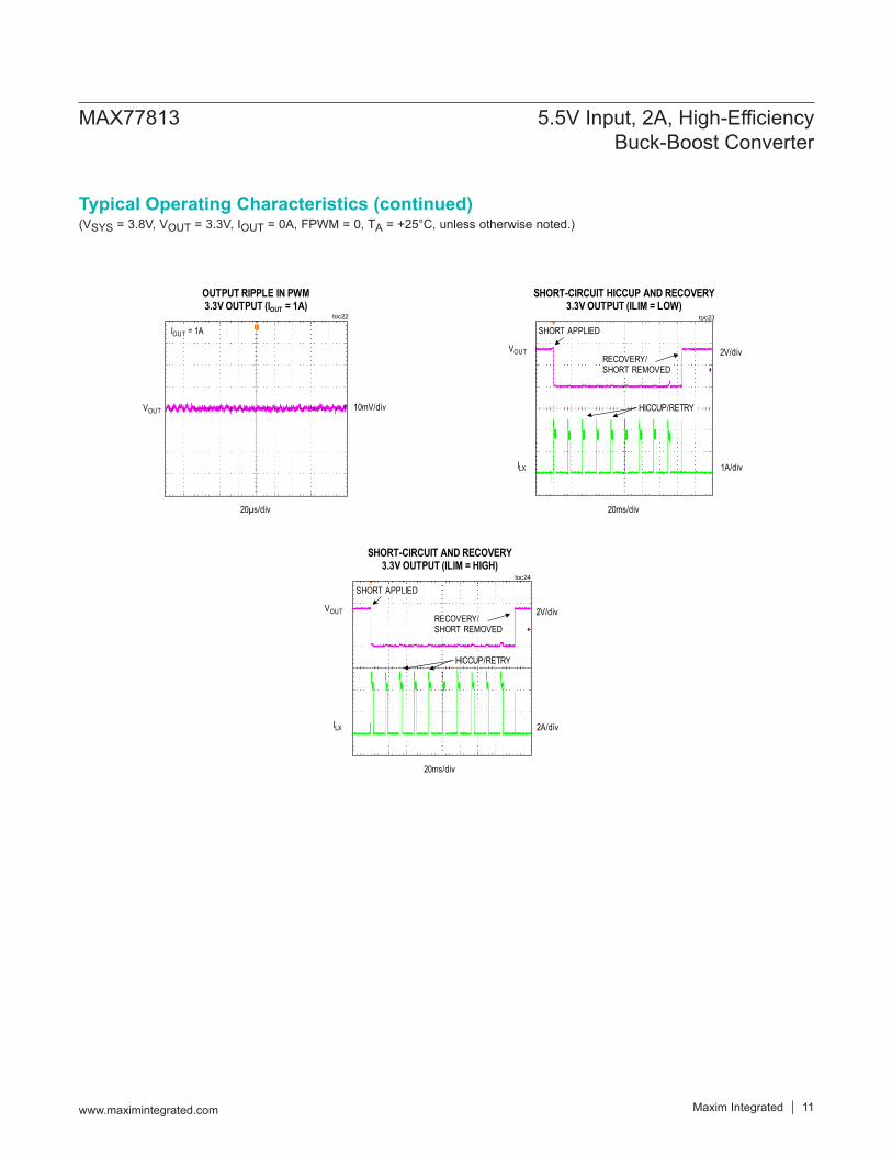
(VSYS = 3.8V, VOUT = 3.3V, IOUT = 0A, FPWM = 0, TA = +25°C, unless otherwise noted.)
Maxim Integrated 9www.maximintegrated.com
MAX77813 5.5V Input, 2A, High-Efficiency Buck-Boost Converter
Typical Operating Characteristics (continued)
0.0
0.5
1.0
1.5
2.0
2.5
3.0
3.5
4.0
4.5
2 3 4 5 6
OUTP
UT C
URRE
NT (A
)
SUPPLY VOLTAGE (V)
VOUT = 2.8VVOUT = 3.3V
VOUT = 5V
MAXIMUM OUTPUT CURRENT vs. SUPPLY VOLTAGE
toc12
ILIM = HIGH
3.26
3.27
3.28
3.29
3.30
3.31
3.32
2.5 3.5 4.5 5.5
OUTP
UT V
OLTA
GE (V
)
SUPPLY VOLTAGE (V)
IOUT = 500mAIOUT = 1AIOUT = 2A
LINE REGULATION 3.3V OUTPUT
toc10
500mA/div
100mV/div
toc14
100µs/div
LOAD TRANSIENT RESPONSE2.8V OUTPUT
VOUT
IOUT
10mA
1A
SLEW RATE = 0.99A/15µs
4.92
4.94
4.96
4.98
5.00
5.02
5.04
2.5 3.5 4.5 5.5OU
TPUT
VOL
TAGE
(V)
SUPPLY VOLTAGE (V)
IOUT = 500mAIOUT = 1AIOUT = 2A
LINE REGULATION 5V OUTPUT
toc11
500mA/div
100mV/div
toc15
100µs/div
LOAD TRANSIENT RESPONSE3.3V OUTPUT
VOUT
IOUT
10mA
1A
SLEW RATE = 0.99A/15µs
2V/div
2A/div
toc13
40µs/div
STARTUP WAVEFORM3.3V OUTPUT
VOUT
VEN
IIN
2V/div
200mV/div
VIN = 3.8V
VLX
EN = 1
(VSYS = 3.8V, VOUT = 3.3V, IOUT = 0A, FPWM = 0, TA = +25°C, unless otherwise noted.)
Maxim Integrated 10www.maximintegrated.com
MAX77813 5.5V Input, 2A, High-Efficiency Buck-Boost Converter
Typical Operating Characteristics (continued)
500mV/div
20mV/div
toc19
100µs/div
BOOST TO BUCK LINE TRANSIENT RESPONSE
VOUT
VIN2.9V
3.4V
IOUT = 1.5AVOUT = 3.3V
SLEW RATE = 20mV/µs
500mA/div
100mV/div
toc16
100µs/div
LOAD TRANSIENT RESPONSE5V OUTPUT
VOUT
IOUT
10mA
1A
SLEW RATE = 0.99A/15µs
500mV/div
20mV/div
toc17
100µs/div
LINE TRANSIENT RESPONSE2.8V OUTPUT
VOUT
VIN2.9V
3.4V
IOUT = 1.5A
SLEW RATE = 20mV/µs
500mV/div
20mV/div
toc18
100µs/div
LINE TRANSIENT RESPONSE5V OUTPUT
VOUT
VIN3.4V
3.9V
IOUT = 1.5A
SLEW RATE = 20mV/µs
1V/div
toc20
100µs/div
SWITCHING WAVEFORM3.3V OUTPUT
VLX
IOUT = 1A
FSW = 2.5MHz
20mV/div
toc21
4µs/div
OUTPUT RIPPLE IN SKIP MODE3.3V OUTPUT (IOUT = 100mA)
VOUT
IOUT = 100mA
(VSYS = 3.8V, VOUT = 3.3V, IOUT = 0A, FPWM = 0, TA = +25°C, unless otherwise noted.)
Maxim Integrated 11www.maximintegrated.com
MAX77813 5.5V Input, 2A, High-Efficiency Buck-Boost Converter
Typical Operating Characteristics (continued)
10mV/div
toc22
20µs/div
OUTPUT RIPPLE IN PWM3.3V OUTPUT (IOUT = 1A)
VOUT
IOUT = 1A
2V/div
1A/div
toc23
20ms/div
SHORT-CIRCUIT HICCUP AND RECOVERY3.3V OUTPUT (ILIM = LOW)
ILX
VOUT
SHORT APPLIED
RECOVERY/SHORT REMOVED
HICCUP/RETRY
2V/div
2A/div
toc24
20ms/div
SHORT-CIRCUIT AND RECOVERY3.3V OUTPUT (ILIM = HIGH)
ILX
VOUT
SHORT APPLIED
RECOVERY/SHORT REMOVED
HICCUP/RETRY
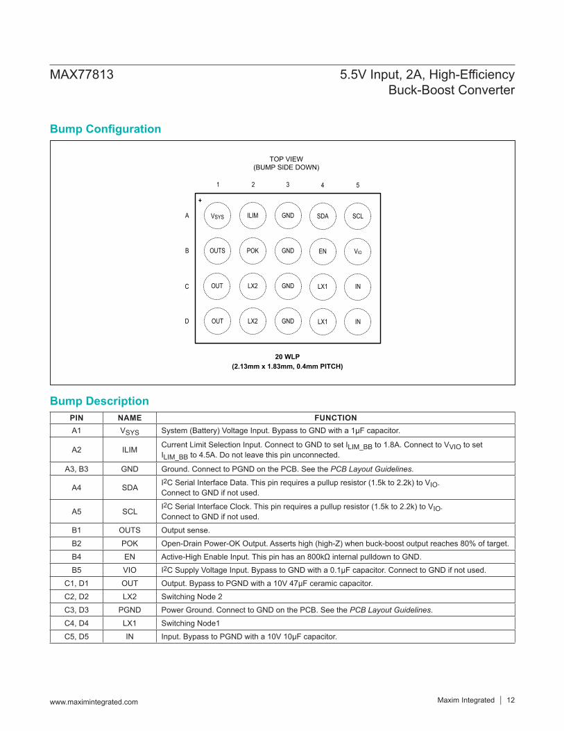
PIN NAME FUNCTIONA1 VSYS System (Battery) Voltage Input. Bypass to GND with a 1µF capacitor.
A2 ILIM Current Limit Selection Input. Connect to GND to set ILIM_BB to 1.8A. Connect to VVIO to set ILIM_BB to 4.5A. Do not leave this pin unconnected.
A3, B3 GND Ground. Connect to PGND on the PCB. See the PCB Layout Guidelines.
A4 SDA I2C Serial Interface Data. This pin requires a pullup resistor (1.5k to 2.2k) to VIO. Connect to GND if not used.
A5 SCL I2C Serial Interface Clock. This pin requires a pullup resistor (1.5k to 2.2k) to VIO. Connect to GND if not used.
B1 OUTS Output sense.B2 POK Open-Drain Power-OK Output. Asserts high (high-Z) when buck-boost output reaches 80% of target. B4 EN Active-High Enable Input. This pin has an 800kΩ internal pulldown to GND. B5 VIO I2C Supply Voltage Input. Bypass to GND with a 0.1µF capacitor. Connect to GND if not used.
C1, D1 OUT Output. Bypass to PGND with a 10V 47µF ceramic capacitor. C2, D2 LX2 Switching Node 2C3, D3 PGND Power Ground. Connect to GND on the PCB. See the PCB Layout Guidelines. C4, D4 LX1 Switching Node1C5, D5 IN Input. Bypass to PGND with a 10V 10µF capacitor.
MAX77813 5.5V Input, 2A, High-Efficiency Buck-Boost Converter
www.maximintegrated.com Maxim Integrated 12
Bump Configuration
Bump Description
20 WLP(2.13mm x 1.83mm, 0.4mm PITCH)
POKOUTS GND
ILIMVSYS GND
1 2 3
A
B
TOP VIEW(BUMP SIDE DOWN)
LX2OUT GND
LX2OUT GNDC
D
EN
SDA
4
LX1
LX1
VIO
SCL
5
IN
IN
+
MAX77813 5.5V Input, 2A, High-Efficiency Buck-Boost Converter
www.maximintegrated.com Maxim Integrated 13
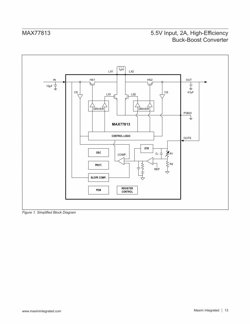
Figure 1. Simplified Block Diagram
OSC
PSM
OUT
PGND
LX2LX1
OUTS
CS CS
IN
CONTROL LOGIC
R1
R2
REF
1µH
47µF
10µF
REGISTER CONTROL
COMP.
DRIVER DRIVER
ETR
HS1 HS2
LS1 LS2
SLOPE COMP.
PROT.
CF
MAX77813
Detailed DescriptionThe MAX77813 is a synchronous step-up/down (buck-boost) DC-DC converter with integrated switches. The buck-boost operates on a supply voltage between 2.3V and 5.5V. Output voltage is configurable through I2C from 2.60V to 5.14V in 20mV steps. Factory-default startup voltage options of 3.3V and 3.4V are available (see the Ordering Information table). The ILIM pin sets the buck-boost switch current capacity.
Strap ILIM high to set 4.5A (typ) switch current. This configuration supports up to 2A out in boost mode and up to 3A out in buck mode.
Strap ILIM low to set 1.8A (typ) switch current. This configuration supports up to 650mA in boost mode and up to 800mA in buck mode.
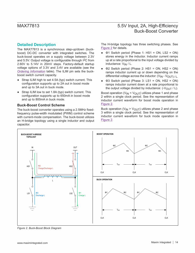
Buck-Boost Control SchemeThe buck-boost converter operates using a 2.5MHz fixed-frequency pulse-width modulated (PWM) control scheme with current-mode compensation. The buck-boost utilizes an H-bridge topology using a single inductor and output capacitor.
The H-bridge topology has three switching phases. See Figure 2 for details.
Φ1 Switch period (Phase 1: HS1 = ON, LS2 = ON) stores energy in the inductor. Inductor current ramps up at a rate proportional to the input voltage divided by inductance: VIN / L.
Φ2 Switch period (Phase 2: HS1 = ON, HS2 = ON) ramps inductor current up or down depending on the differential voltage across the inductor: (VIN - VOUT) / L.
Φ3 Switch period (Phase 3: LS1 = ON, HS2 = ON) ramps inductor current down at a rate proportional to the output voltage divided by inductance: (-VOUT / L).
Boost operation (VIN < VOUT) utilizes phase 1 and phase 2 within a single clock period. See the representation of inductor current waveform for boost mode operation in Figure 2.Buck operation (VIN > VOUT) utilizes phase 2 and phase 3 within a single clock period. See the representation of inductor current waveform for buck mode operation in Figure 2.
Figure 2. Buck-Boost Block Diagram
MAX77813 5.5V Input, 2A, High-Efficiency Buck-Boost Converter
www.maximintegrated.com Maxim Integrated 14
IN OUT
HS2
LS2
L
Ф2 Charge/Discharge L
Ф1 Charge L
Ф3Discharge L
CLK CLK
TSW
Ф2
Ф3
CLK
TSW
Ф2
Ф3
CLK CLK
TSW
Ф2 Ф1
CLK
TSW
Ф2Ф1
HS1
LS1
BOOST OPERATION
BUCK OPERATION
BUCK-BOOST H-BRIDGE TOPOLOGY
Enable Control (EN)Raise the EN pin voltage above VIH threshold to enable the buck-boost output. Lower EN below VIL threshold to disable. EN has an internal 800kΩ (typ) pulldown resistor to GND. Clear the EN bit using the I2C interface to disable the internal pulldown (making EN high-impedance). The EN_PD bit reset value is 1 (pulldown enabled). Therefore, the internal pulldown resistor is present whenever the MAX77813 starts up. After the initial buck-boost startup, clear the EN bit through I2C to disable the buck-boost output. Table 1 details the interaction between the EN pin and the EN bit. Provide a valid VIO and set the EN pin logic-high to enable the I2C serial interface. Serial reads and writes to the EN bit may happen only while VIO is valid and EN is logic-high. Lowering EN logic-low disables the buck-boost (regardless of EN) and causes all registers to reset to default values.
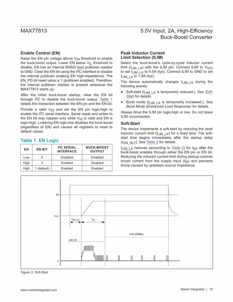
Peak Inductor Current Limit Selection (ILIM)Select the buck-boost’s cycle-by-cycle inductor current limit (ILIM_LX) with the ILIM pin. Connect ILIM to VVIO to set ILIM_LX to 4.5A (typ). Connect ILIM to GND to set ILIM_LX to 1.8A (typ). The device automatically changes ILIM_LX during the following events:
Soft-start (ILIM_LX is temporarily reduced.). See Soft-Start for details.
Burst mode (ILIM_LX is temporarily increased.). See Burst Mode (Enhanced Load Response) for details.
Always drive the ILIM pin logic-high or low. Do not leave ILIM unconnected.
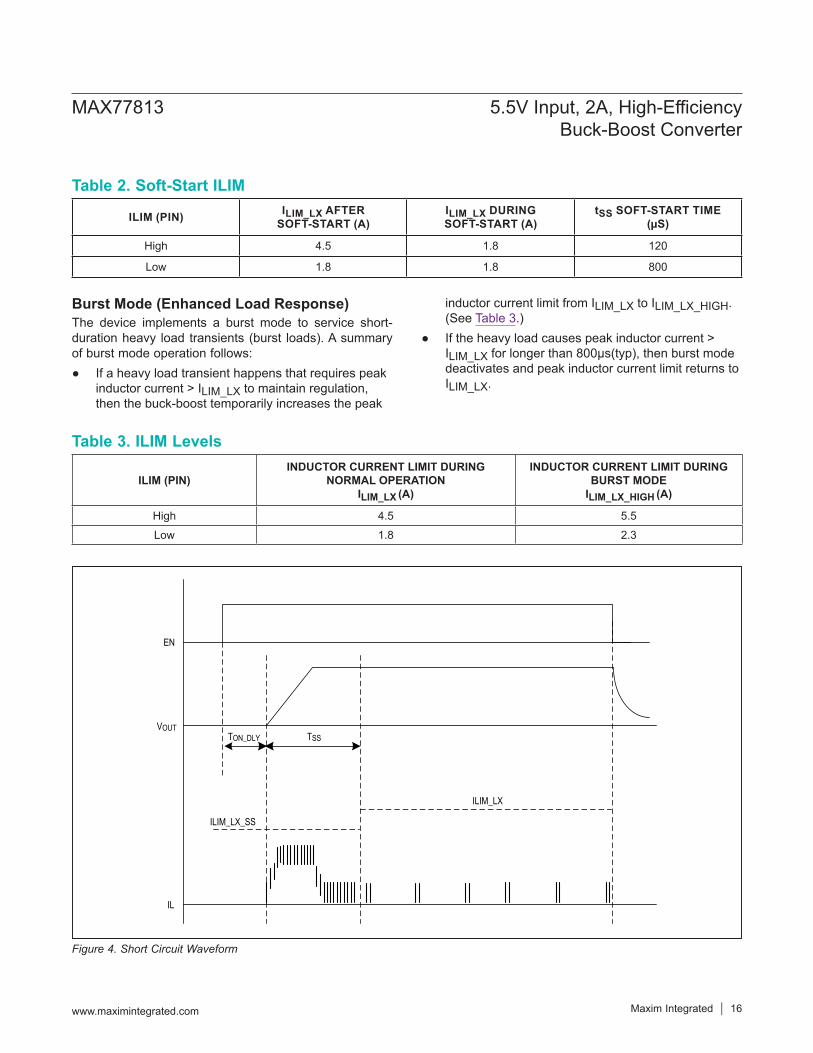
Soft-Start The device implements a soft-start by reducing the peak inductor current limit (ILIM_LX) for a fixed time. The soft-start time begins immediately after the startup delay (tON_DLY). See Table 2 for details.ILIM_LX reduces (according to Table 2) for tSS after the buck-boost enables through either the EN pin or EN bit. Reducing the inductor current limit during startup controls inrush current from the supply input (IIN) and prevents droop caused by upstream source impedance.
Table 1. EN Logic
EN EN BIT I2C SERIAL INTERFACE
BUCK-BOOST OUTPUT
Low X Disabled DisabledHigh 0 Enabled DisabledHigh 1 (default) Enabled Enabled
Figure 3. Soft-Start
MAX77813 5.5V Input, 2A, High-Efficiency Buck-Boost Converter
www.maximintegrated.com Maxim Integrated 15
EN
VOUTTON_DLY TSS
IL
ILIM_SS
ILIM_NORMAL
Burst Mode (Enhanced Load Response) The device implements a burst mode to service short-duration heavy load transients (burst loads). A summary of burst mode operation follows:
If a heavy load transient happens that requires peak inductor current > ILIM_LX to maintain regulation, then the buck-boost temporarily increases the peak
inductor current limit from ILIM_LX to ILIM_LX_HIGH. (See Table 3.)
If the heavy load causes peak inductor current > ILIM_LX for longer than 800µs(typ), then burst mode deactivates and peak inductor current limit returns to ILIM_LX.
Table 2. Soft-Start ILIM
Table 3. ILIM Levels
ILIM (PIN) ILIM_LX AFTER SOFT-START (A)
ILIM_LX DURING SOFT-START (A)
tSS SOFT-START TIME (µS)
High 4.5 1.8 120
Low 1.8 1.8 800
ILIM (PIN)INDUCTOR CURRENT LIMIT DURING
NORMAL OPERATIONILIM_LX (A)
INDUCTOR CURRENT LIMIT DURING BURST MODE
ILIM_LX_HIGH (A)
High 4.5 5.5Low 1.8 2.3
Figure 4. Short Circuit Waveform
MAX77813 5.5V Input, 2A, High-Efficiency Buck-Boost Converter
www.maximintegrated.com Maxim Integrated 16
EN
VOUTTON_DLY TSS
IL
ILIM_LX_SS
ILIM_LX
Power-OK (POK) OutputThe device features an open-drain POK output to monitor the output voltage. POK requires an external pullup resis-tor (typically 10kΩ to 100kΩ). POK is active-high by default. Use the POK_POL bit to change the POK polarity to active-low. See the Register Map for details. While POK_POL = 1 (active-high, default state), POK goes high (high-impedance) after the buck-boost output increases above 80% of the target regulation voltage. POK goes low when the output drops below 75% of the target or when the buck-boost is disabled.
Output Voltage Selection and Slew Rate ControlWrite the VOUT[6:0] bitfield through I2C to configure the target output voltage (VOUT) between 2.60V and 5.14V in 20mV steps. The default value of VOUT[6:0] is factory-programmable. See the Ordering Information for the default VOUT associated with each orderable part num-ber. Overwriting the default value through I2C sets a new target VOUT until registers reset.Changing the VOUT[6:0] bitfield while the buck-boost output is enabled causes the device to respond in the following way:
VOUT ramps up at a rate set by RU_SR (20mV/μs or 40mV/μs) when the VOUT target is increased.
VOUT ramps down at a rate set by RD_SR (5mV/μs or 10mV/μs) when the VOUT target is decreased.
See the Register Map for details about the RU_SR and RD_SR bits.
Output Overvoltage Protection (OVP)The device has an internal output overvoltage protection (OVP) circuit which monitors VOUT for overvoltage faults. The buck-boost disables if the output exceeds the over-voltage threshold set by the OVP_TH[1:0] bitfield.
Disable OVP by programming OVP_TH[1:0] to 0b00 using I2C. The default OVP threshold is 0b11 (120% of the target VOUT). The OVP status bit continuously mirrors the status of the OVP circuit. See the Register Map for details.
Thermal ShutdownThe device has an internal thermal protection circuit which monitors die temperature. The buck-boost disables if the die temperature exceeds TSHDN (165°C typ). The buck-boost enables again after the die temperature cools by approximately 20°C. The TSHDN status bit continuously mirrors the status of the thermal protection circuit. See the Register Map for details.
I2C Serial InterfaceThe device features a revision 3.0 I2C-compatible, 2-wire serial interface consisting of a bidirectional serial data line (SDA) and a serial clock line (SCL). The MAX77813 is a slave-only device that that relies on an external bus mas-ter to generate SCL. SCL clock rates from 0Hz to 3.4MHz are supported. I2C is an open-drain bus, and therefore, SDA and SCL require pullups (500Ω or greater). The device’s I2C communication controller implements 7-bit slave addressing. An I2C bus master initiates com-munication with the slave by issuing a START condition followed by the slave address. The slave address of the device is shown in Table 4. The device uses 8-bit registers with 8-bit register address-ing. They support standard communication protocols: (1) Writing to a single register (2) Writing to multiple sequen-tial registers with an automatically incrementing data pointer (3) Reading from a single register (4) Reading from multiple sequential registers with an automati-cally incrementing data pointer. For additional informa-tion on the I2C protocols, refer to the MAX77813 I2C Implementer’s Guide and/or the I2C specification that is freely available on the internet.
Table 4. I2C Slave Address
ILIM (PIN)INDUCTOR CURRENT LIMIT DURING
NORMAL OPERATIONILIM_LX (A)
INDUCTOR CURRENT LIMIT DURING BURST MODE
ILIM_LX_HIGH (A)
High 4.5 5.5Low 1.8 2.3
MAX77813 5.5V Input, 2A, High-Efficiency Buck-Boost Converter
www.maximintegrated.com Maxim Integrated 17
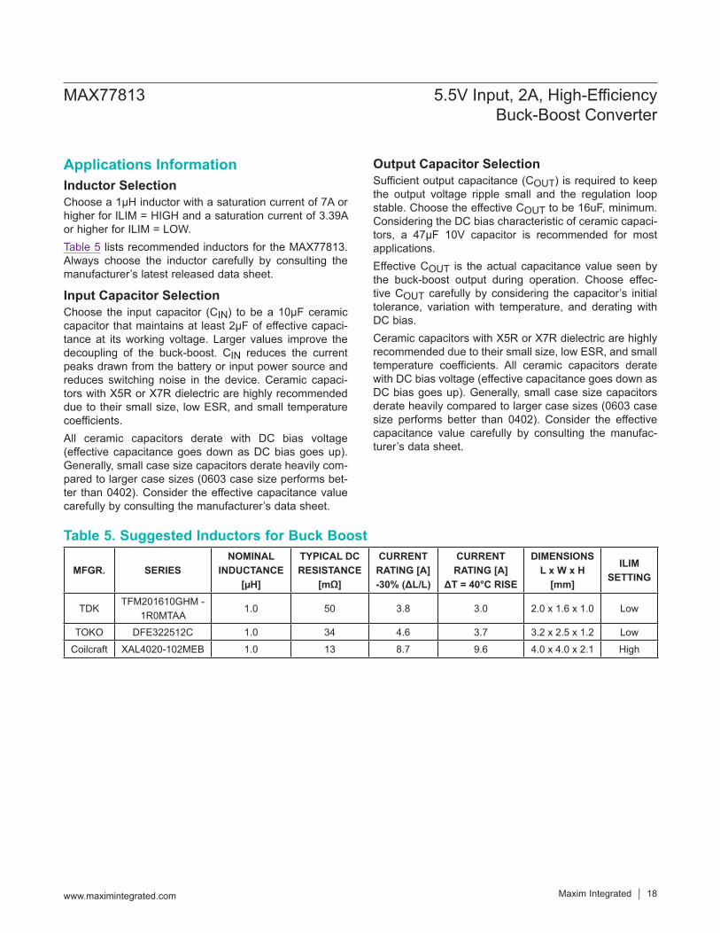
Applications InformationInductor SelectionChoose a 1μH inductor with a saturation current of 7A or higher for ILIM = HIGH and a saturation current of 3.39A or higher for ILIM = LOW. Table 5 lists recommended inductors for the MAX77813. Always choose the inductor carefully by consulting the manufacturer’s latest released data sheet.
Input Capacitor SelectionChoose the input capacitor (CIN) to be a 10μF ceramic capacitor that maintains at least 2μF of effective capaci-tance at its working voltage. Larger values improve the decoupling of the buck-boost. CIN reduces the current peaks drawn from the battery or input power source and reduces switching noise in the device. Ceramic capaci-tors with X5R or X7R dielectric are highly recommended due to their small size, low ESR, and small temperature coefficients.All ceramic capacitors derate with DC bias voltage (effective capacitance goes down as DC bias goes up). Generally, small case size capacitors derate heavily com-pared to larger case sizes (0603 case size performs bet-ter than 0402). Consider the effective capacitance value carefully by consulting the manufacturer’s data sheet.
Output Capacitor SelectionSufficient output capacitance (COUT) is required to keep the output voltage ripple small and the regulation loop stable. Choose the effective COUT to be 16uF, minimum. Considering the DC bias characteristic of ceramic capaci-tors, a 47μF 10V capacitor is recommended for most applications.Effective COUT is the actual capacitance value seen by the buck-boost output during operation. Choose effec-tive COUT carefully by considering the capacitor’s initial tolerance, variation with temperature, and derating with DC bias. Ceramic capacitors with X5R or X7R dielectric are highly recommended due to their small size, low ESR, and small temperature coefficients. All ceramic capacitors derate with DC bias voltage (effective capacitance goes down as DC bias goes up). Generally, small case size capacitors derate heavily compared to larger case sizes (0603 case size performs better than 0402). Consider the effective capacitance value carefully by consulting the manufac-turer’s data sheet.
Table 5. Suggested Inductors for Buck Boost
MFGR. SERIESNOMINAL
INDUCTANCE [µH]
TYPICAL DCRESISTANCE
[mΩ]
CURRENT RATING [A]-30% (ΔL/L)
CURRENT RATING [A]
ΔT = 40°C RISE
DIMENSIONSL x W x H
[mm]
ILIM SETTING
TDKTFM201610GHM -
1R0MTAA1.0 50 3.8 3.0 2.0 x 1.6 x 1.0 Low
TOKO DFE322512C 1.0 34 4.6 3.7 3.2 x 2.5 x 1.2 LowCoilcraft XAL4020-102MEB 1.0 13 8.7 9.6 4.0 x 4.0 x 2.1 High
MAX77813 5.5V Input, 2A, High-Efficiency Buck-Boost Converter
www.maximintegrated.com Maxim Integrated 18
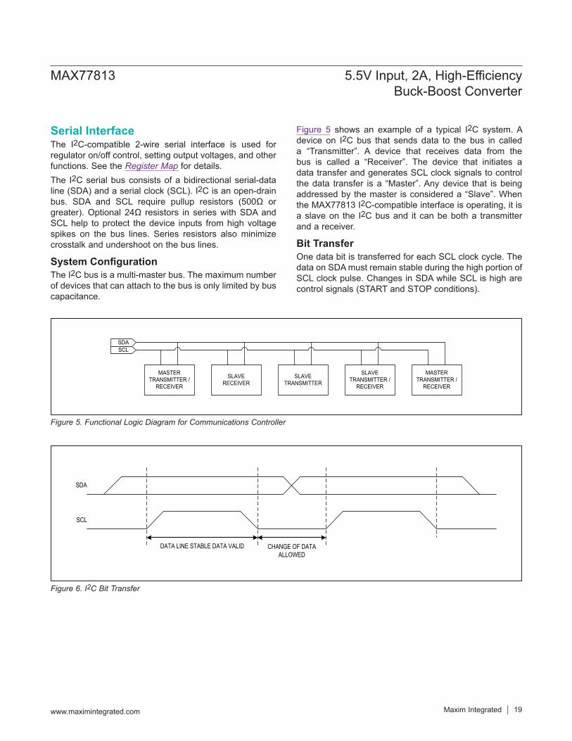
Serial InterfaceThe I2C-compatible 2-wire serial interface is used for regulator on/off control, setting output voltages, and other functions. See the Register Map for details. The I2C serial bus consists of a bidirectional serial-data line (SDA) and a serial clock (SCL). I2C is an open-drain bus. SDA and SCL require pullup resistors (500Ω or greater). Optional 24Ω resistors in series with SDA and SCL help to protect the device inputs from high voltage spikes on the bus lines. Series resistors also minimize crosstalk and undershoot on the bus lines.
System ConfigurationThe I2C bus is a multi-master bus. The maximum number of devices that can attach to the bus is only limited by bus capacitance.
Figure 5 shows an example of a typical I2C system. A device on I2C bus that sends data to the bus in called a “Transmitter”. A device that receives data from the bus is called a “Receiver”. The device that initiates a data transfer and generates SCL clock signals to control the data transfer is a “Master”. Any device that is being addressed by the master is considered a “Slave”. When the MAX77813 I2C-compatible interface is operating, it is a slave on the I2C bus and it can be both a transmitter and a receiver.
Bit TransferOne data bit is transferred for each SCL clock cycle. The data on SDA must remain stable during the high portion of SCL clock pulse. Changes in SDA while SCL is high are control signals (START and STOP conditions).
Figure 5. Functional Logic Diagram for Communications Controller
Figure 6. I2C Bit Transfer
MAX77813 5.5V Input, 2A, High-Efficiency Buck-Boost Converter
www.maximintegrated.com Maxim Integrated 19
MASTER TRANSMITTER /
RECEIVER
SDASCL
SLAVE RECEIVER
SLAVE TRANSMITTER
SLAVE TRANSMITTER /
RECEIVER
MASTER TRANSMITTER /
RECEIVER
SDA
SCL
CHANGE OF DATA ALLOWED
DATA LINE STABLE DATA VALID
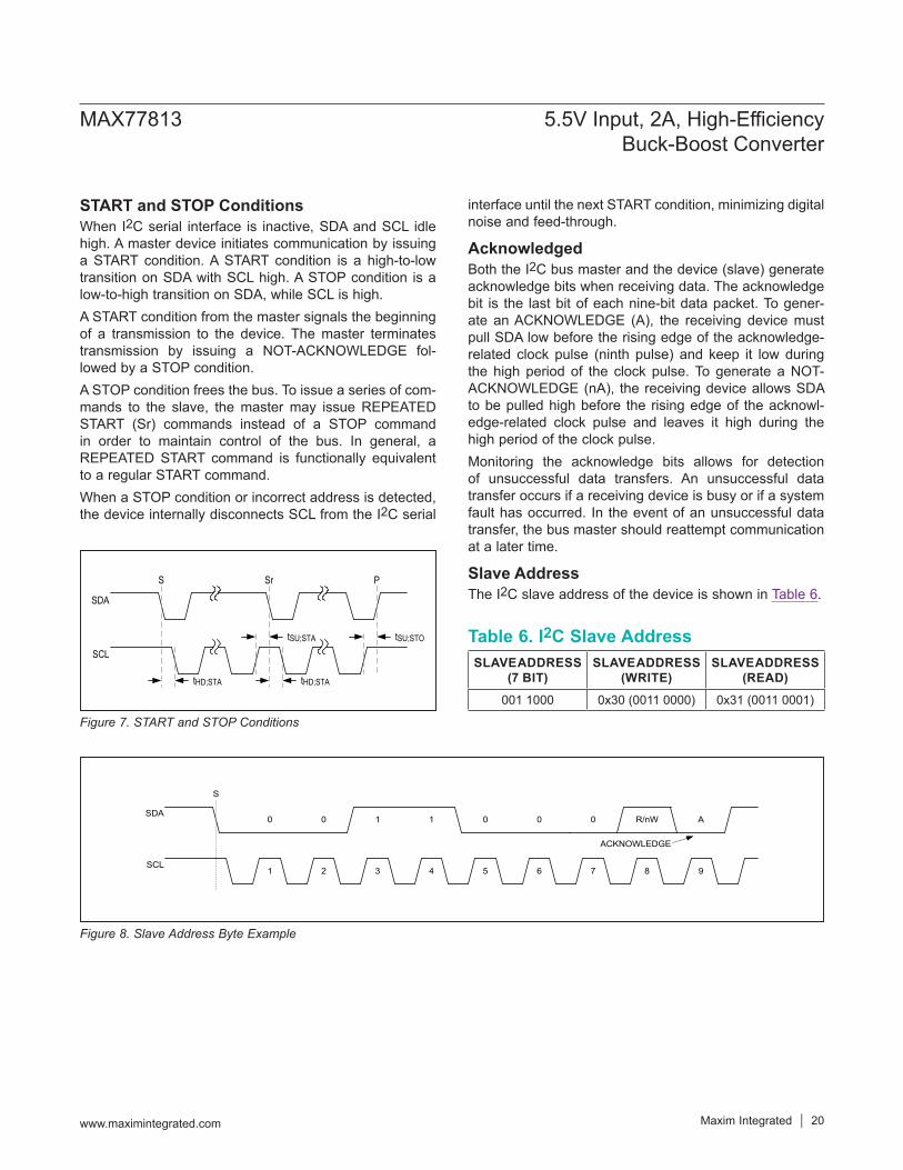
START and STOP Conditions When I2C serial interface is inactive, SDA and SCL idle high. A master device initiates communication by issuing a START condition. A START condition is a high-to-low transition on SDA with SCL high. A STOP condition is a low-to-high transition on SDA, while SCL is high.A START condition from the master signals the beginning of a transmission to the device. The master terminates transmission by issuing a NOT-ACKNOWLEDGE fol-lowed by a STOP condition.A STOP condition frees the bus. To issue a series of com-mands to the slave, the master may issue REPEATED START (Sr) commands instead of a STOP command in order to maintain control of the bus. In general, a REPEATED START command is functionally equivalent to a regular START command.When a STOP condition or incorrect address is detected, the device internally disconnects SCL from the I2C serial
interface until the next START condition, minimizing digital noise and feed-through.
AcknowledgedBoth the I2C bus master and the device (slave) generate acknowledge bits when receiving data. The acknowledge bit is the last bit of each nine-bit data packet. To gener-ate an ACKNOWLEDGE (A), the receiving device must pull SDA low before the rising edge of the acknowledge-related clock pulse (ninth pulse) and keep it low during the high period of the clock pulse. To generate a NOT-ACKNOWLEDGE (nA), the receiving device allows SDA to be pulled high before the rising edge of the acknowl-edge-related clock pulse and leaves it high during the high period of the clock pulse.Monitoring the acknowledge bits allows for detection of unsuccessful data transfers. An unsuccessful data transfer occurs if a receiving device is busy or if a system fault has occurred. In the event of an unsuccessful data transfer, the bus master should reattempt communication at a later time.
Slave AddressThe I2C slave address of the device is shown in Table 6.
Table 6. I2C Slave AddressSLAVE ADDRESS
(7 BIT)SLAVE ADDRESS
(WRITE)SLAVE ADDRESS
(READ)001 1000 0x30 (0011 0000) 0x31 (0011 0001)
Figure 7. START and STOP Conditions
Figure 8. Slave Address Byte Example
MAX77813 5.5V Input, 2A, High-Efficiency Buck-Boost Converter
www.maximintegrated.com Maxim Integrated 20
S PSr
SCL
SDA
tHD;STA
tSU;STA tSU;STO
tHD;STA
S
SCL
SDA
1 2 3
100
8 9
ACKNOWLEDGE
4 5 6 7
1 0 0 R/nW A0
Clock StretchingIn general, the clock signal generation for the I2C bus is the responsibility of the master device. I2C specification allows slow slave devices to alter the clock signal by holding down the clock line. The process in which a slave device holds down the clock line is typically called clock stretching. The device does not use any form of clock stretching to hold down the clock line.
General Call AddressThe device does not implement I2C specification “General Call Address.” If the device sees “General Call Address (00000000b)” it does not issue an ACKNOWLEDGE (A).
Communication SpeedThe device provides I2C 3.0-compatible (3.4MHz) serial interface.
I2C Revision 3 Compatible Serial Communications Channel• 0Hz to 100kHz (Standard mode)• 0Hz to 400kHz (Fast mode)• 0Hz to 1MHz (Fast-mode plus)• 0Hz to 3.4MHz (High-speed mode)
Does not utilize I2C Clock StretchingOperating in standard mode, fast mode, and fast-mode plus does not require any special protocols. The main consideration when changing the bus speed through this range is the combination of the bus capacitance and pullup resistors. Higher time constants created by the bus capacitance and pullup resistance (C x R) slow the bus operation. Therefore, when increasing bus speeds, the pullup resistance must be decreased to maintain a reasonable time constant. See the Pullup Resistor Sizing
section of the I2C revision 3.0 specification for detailed guidance on the pullup resistor selection. In general, for bus capacitances of 200pF, a 100kHz bus needs 5.6kΩ pullup resistors, a 400kHz bus needs about 1.5kΩ pullup resistors, and a 1MHz bus needs 680Ω pullup resistors. Note that the pullup resistor is dissipating power when the open-drain bus is low. The lower the value of the pullup resistor, the higher the power dissipation (V2/R).Operating in high-speed mode requires some special con-siderations. For the full list of considerations, see the I2C 3.0 specification. The major considerations with respect to the MAX77813 are:
I2C bus master use current source pullups to shorten the signal rise times.
I2C slave must use a different set of input filters on its SDA and SCL lines to accommodate for the higher bus speed.
The communication protocols need to utilize the high-speed master code.
At power-up and after each STOP condition, the device input filters are set for standard mode, fast mode, or fast-mode plus (i.e., 0Hz to 1MHz). To switch the input filters for high-speed mode, use the high-speed master code protocols that are described in the Communication Protocols section.
Communication ProtocolsThe device supports both writing and reading from its reg-isters. The following sections show the I2C communica-tion protocols for each functional block. The power block uses the same communication protocols.
MAX77813 5.5V Input, 2A, High-Efficiency Buck-Boost Converter
www.maximintegrated.com Maxim Integrated 21
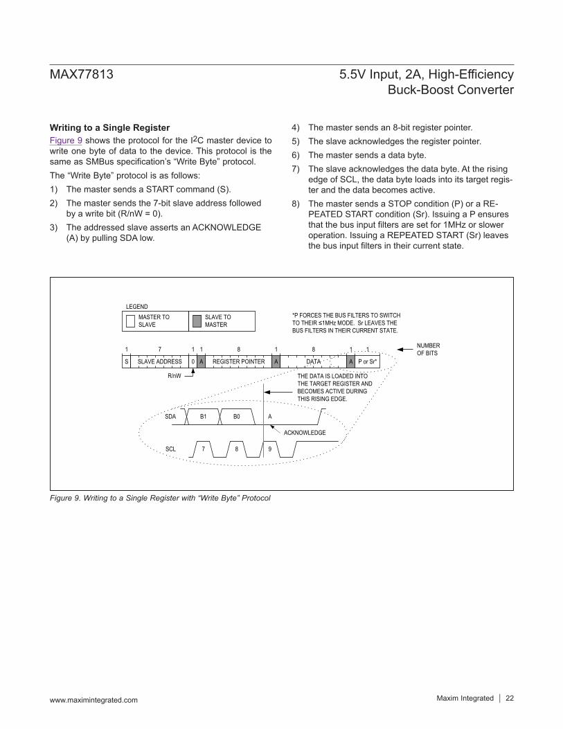
Writing to a Single RegisterFigure 9 shows the protocol for the I2C master device to write one byte of data to the device. This protocol is the same as SMBus specification’s “Write Byte” protocol.The “Write Byte” protocol is as follows:1) The master sends a START command (S).2) The master sends the 7-bit slave address followed
by a write bit (R/nW = 0).3) The addressed slave asserts an ACKNOWLEDGE
(A) by pulling SDA low.
4) The master sends an 8-bit register pointer.5) The slave acknowledges the register pointer.6) The master sends a data byte.7) The slave acknowledges the data byte. At the rising
edge of SCL, the data byte loads into its target regis-ter and the data becomes active.
8) The master sends a STOP condition (P) or a RE-PEATED START condition (Sr). Issuing a P ensures that the bus input filters are set for 1MHz or slower operation. Issuing a REPEATED START (Sr) leaves the bus input filters in their current state.
Figure 9. Writing to a Single Register with “Write Byte” Protocol
MAX77813 5.5V Input, 2A, High-Efficiency Buck-Boost Converter
www.maximintegrated.com Maxim Integrated 22
1
S
NUMBER OF BITS
R/nW
SLAVE ADDRESS
7
0
1 8
REGISTER POINTERA
1
A
1 8
DATA
1
P or Sr*
*P FORCES THE BUS FILTERS TO SWITCH TO THEIR ≤1MHz MODE. Sr LEAVES THE BUS FILTERS IN THEIR CURRENT STATE.
SLAVE TO MASTER
MASTER TO SLAVE
LEGEND
8 97
B0 AB1
THE DATA IS LOADED INTO THE TARGET REGISTER AND BECOMES ACTIVE DURING THIS RISING EDGE.
SDA
SCL
ACKNOWLEDGE
A
1
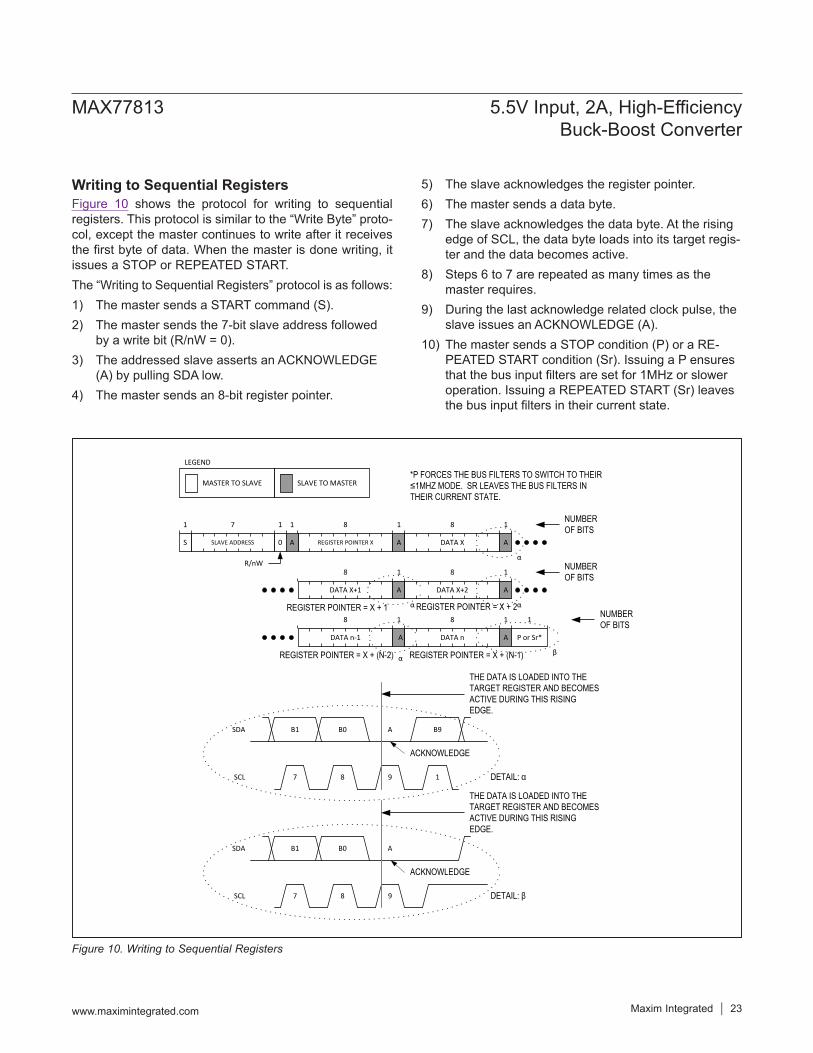
Writing to Sequential RegistersFigure 10 shows the protocol for writing to sequential registers. This protocol is similar to the “Write Byte” proto-col, except the master continues to write after it receives the first byte of data. When the master is done writing, it issues a STOP or REPEATED START.The “Writing to Sequential Registers” protocol is as follows:1) The master sends a START command (S).2) The master sends the 7-bit slave address followed
by a write bit (R/nW = 0).3) The addressed slave asserts an ACKNOWLEDGE
(A) by pulling SDA low.4) The master sends an 8-bit register pointer.
5) The slave acknowledges the register pointer.6) The master sends a data byte.7) The slave acknowledges the data byte. At the rising
edge of SCL, the data byte loads into its target regis-ter and the data becomes active.
8) Steps 6 to 7 are repeated as many times as the master requires.
9) During the last acknowledge related clock pulse, the slave issues an ACKNOWLEDGE (A).
10) The master sends a STOP condition (P) or a RE-PEATED START condition (Sr). Issuing a P ensures that the bus input filters are set for 1MHz or slower operation. Issuing a REPEATED START (Sr) leaves the bus input filters in their current state.
Figure 10. Writing to Sequential Registers
MAX77813 5.5V Input, 2A, High-Efficiency Buck-Boost Converter
www.maximintegrated.com Maxim Integrated 23
1
S
NUMBER OF BITS
R/nW
SLAVE ADDRESS
7
0
1 8
REGISTER POINTER XA
1
A
1 8
DATA X A
1
NUMBER OF BITS8
DATA X+1 A
1 8
DATA X+2 A
1
NUMBER OF BITS8
DATA n-1 A
1 8
DATA n
α
αα
αβ
1
P or Sr*
*P FORCES THE BUS FILTERS TO SWITCH TO THEIR ≤1MHZ MODE. SR LEAVES THE BUS FILTERS IN THEIR CURRENT STATE.
REGISTER POINTER = X + 1 REGISTER POINTER = X + 2
REGISTER POINTER = X + (N-2) REGISTER POINTER = X + (N-1)
SLAVE TO MASTERMASTER TO SLAVE
LEGEND
8 97
B0 AB1
THE DATA IS LOADED INTO THE TARGET REGISTER AND BECOMES ACTIVE DURING THIS RISING EDGE.
SDA
SCL DETAIL: α
DETAIL: β
1
B9
8 97
B0 AB1
THE DATA IS LOADED INTO THE TARGET REGISTER AND BECOMES ACTIVE DURING THIS RISING EDGE.
SDA
SCL
ACKNOWLEDGE
ACKNOWLEDGE
A
1
Reading from a Single RegisterThe I2C master device reads one byte of data to the device. This protocol is the same as SMBus specifica-tion’s “Read Byte” protocol.The “Read Byte” protocol is as follows:1) The master sends a START command (S).2) The master sends the 7-bit slave address followed
by a write bit (R/nW = 0).3) The addressed slave asserts an ACKNOWLEDGE
(A) by pulling SDA low.4) The master sends an 8-bit register pointer.5) The slave acknowledges the register pointer.6) The master sends a REPEATED START command
(Sr).7) The master sends the 7-bit slave address followed
by a read bit (R/nW = 1).8) The addressed slave asserts an ACKNOWLEDGE
(A) by pulling SDA low.9) The addressed slave places 8-bits of data on the bus
from the location specified by the register pointer.10) The master issues a NOT-ACKNOWLEDGE (nA).11) The master sends a STOP condition (P) or a RE-
PEATED START condition (Sr). Issuing a P ensures that the bus input filters are set for 1MHz or slower operation. Issuing a REPEATED START (Sr) leaves the bus input filters in their current state.
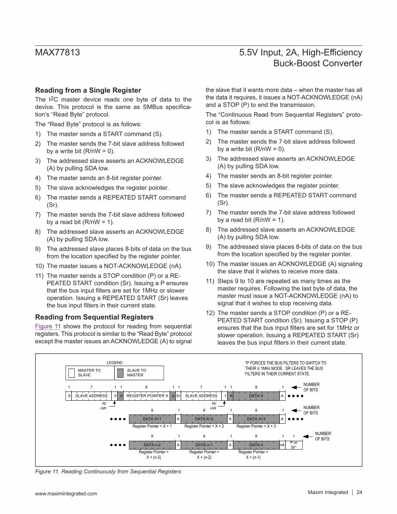
Reading from Sequential RegistersFigure 11 shows the protocol for reading from sequential registers. This protocol is similar to the “Read Byte” protocol except the master issues an ACKNOWLEDGE (A) to signal
the slave that it wants more data – when the master has all the data it requires, it issues a NOT-ACKNOWLEDGE (nA) and a STOP (P) to end the transmission.The “Continuous Read from Sequential Registers” proto-col is as follows:1) The master sends a START command (S).2) The master sends the 7-bit slave address followed
by a write bit (R/nW = 0).3) The addressed slave asserts an ACKNOWLEDGE
(A) by pulling SDA low.4) The master sends an 8-bit register pointer.5) The slave acknowledges the register pointer.6) The master sends a REPEATED START command
(Sr).7) The master sends the 7-bit slave address followed
by a read bit (R/nW = 1).8) The addressed slave asserts an ACKNOWLEDGE
(A) by pulling SDA low.9) The addressed slave places 8-bits of data on the bus
from the location specified by the register pointer.10) The master issues an ACKNOWLEDGE (A) signaling
the slave that it wishes to receive more data.11) Steps 9 to 10 are repeated as many times as the
master requires. Following the last byte of data, the master must issue a NOT-ACKNOWLEDGE (nA) to signal that it wishes to stop receiving data.
12) The master sends a STOP condition (P) or a RE-PEATED START condition (Sr). Issuing a STOP (P) ensures that the bus input filters are set for 1MHz or slower operation. Issuing a REPEATED START (Sr) leaves the bus input filters in their current state.
Figure 11. Reading Continuously from Sequential Registers
MAX77813 5.5V Input, 2A, High-Efficiency Buck-Boost Converter
www.maximintegrated.com Maxim Integrated 24
1
S
R/nW
SLAVE ADDRESS
7
0
1 8
REGISTER POINTER XA
1
A
1 1
Sr SLAVE ADDRESS
7
1
1 8
DATA XA
1
A
1 NUMBER OF BITS
R/nW 8
DATA X+3 A
1 NUMBER OF BITS8
DATA X+2 A
1
DATA X+1 A
8 1
8
DATA n nA
18
DATA n-1 A
1
DATA n-2 A
8 1
SLAVE TO MASTER
MASTER TO SLAVE
LEGEND
NUMBER OF BITS1
P or Sr*
*P FORCES THE BUS FILTERS TO SWITCH TO THEIR ≤ 1MHz MODE. SR LEAVES THE BUS FILTERS IN THEIR CURRENT STATE.
Register Pointer = X + 1 Register Pointer = X + 2 Register Pointer = X + 3
Register Pointer = X + (n-3)
Register Pointer = X + (n-2)
Register Pointer = X + (n-1)
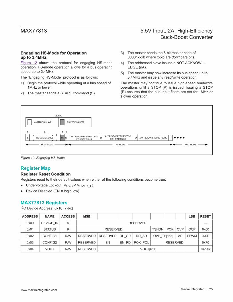
Engaging HS-Mode for Operation up to 3.4MHzFigure 12 shows the protocol for engaging HS-mode operation. HS-mode operation allows for a bus operating speed up to 3.4MHz.The “Engaging HS-Mode” protocol is as follows:1) Begin the protocol while operating at a bus speed of
1MHz or lower.2) The master sends a START command (S).
3) The master sends the 8-bit master code of 00001xxxb where xxxb are don’t care bits.
4) The addressed slave issues a NOT-ACKNOWL-EDGE (nA).
5) The master may now increase its bus speed up to 3.4MHz and issue any read/write operation.
The master may continue to issue high-speed read/write operations until a STOP (P) is issued. Issuing a STOP (P) ensures that the bus input filters are set for 1MHz or slower operation.
Register Reset ConditionRegisters reset to their default values when either of the following conditions become true:
Undervoltage Lockout (VSYS < VUVLO_F) Device Disabled (EN = logic low)
MAX77813 Registers I2C Device Address: 0x18 (7-bit)
ADDRESS NAME ACCESS MSB LSB RESET
0x00 DEVICE_ID R RESERVED —
0x01 STATUS R RESERVED TSHDN POK OVP OCP 0x00
0x02 CONFIG1 R/W RESERVED RESERVED RU_SR RD_SR OVP_TH[1:0] AD FPWM 0x0E
0x03 CONFIG2 R/W RESERVED EN EN_PD POK_POL RESERVED 0x70
0x04 VOUT R/W RESERVED VOUT[6:0] varies
Figure 12. Engaging HS-Mode
MAX77813 5.5V Input, 2A, High-Efficiency Buck-Boost Converter
www.maximintegrated.com Maxim Integrated 25
Register Map
1
S HS-MASTER CODE
8
nA
1 1
Sr
SLAVE TO MASTERMASTER TO SLAVE
LEGEND
FAST- MODE HS-MODE
Sr Sr ANY READ/WRITE PROTOCOL P
FAST-MODE
ANY READ/WRITE PROTOCOLFOLLOWED BY Sr
ANY READ/WRITE PROTOCOL FOLLOWED BY Sr
Register DetailsDEVICE ID (0x00)
STATUS (0x01)
BIT 7 6 5 4 3 2 1 0
Field RESERVED[7:0]
Reset —
Access Read Only
BIT 7 6 5 4 3 2 1 0
Field RESERVED[3:0] TSHDN POK OVP OCP
Reset 0b0000 0b0 0b0 0b0 0b0
Access Read Only Read Only Read Only Read Only Read Only
BITFIELD BITS DESCRIPTION DECODE
RESERVED 7:0 Reserved. Bits for internal use only. N/A
BITFIELD BITS DESCRIPTION DECODE
RESERVED 3:0 Reserved. Reads are don’t care. N/A
TSHDN 3 Thermal Shutdown Status 0 = Junction temperature OK (TJ < TSHDN)1 = Thermal shutdown (TJ ≥ TSHDN)
POKn 2 Power-OK Status 0 = Output not OK (VOUT < 75% of target) or disabled.1 = Output OK (VOUT > 80% of target)
OVP 1 Output Overvoltage Status
0 = Output OK (VOUT < the OVP threshold set by OVP_TH[1:0]) or disabled. 1 = Output overvoltage. VOUT > the OVP threshold set by OVP_TH[1:0].
OCP 0 Overcurrent Status 0 = Current OK1 = Overcurrent
MAX77813 5.5V Input, 2A, High-Efficiency Buck-Boost Converter
www.maximintegrated.com Maxim Integrated 26
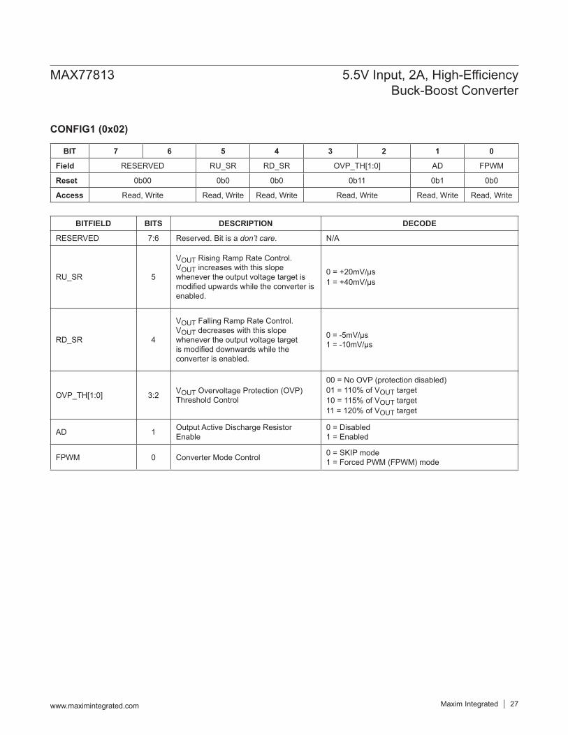
BIT 7 6 5 4 3 2 1 0
Field RESERVED RU_SR RD_SR OVP_TH[1:0] AD FPWM
Reset 0b00 0b0 0b0 0b11 0b1 0b0
Access Read, Write Read, Write Read, Write Read, Write Read, Write Read, Write
BITFIELD BITS DESCRIPTION DECODE
RESERVED 7:6 Reserved. Bit is a don’t care. N/A
RU_SR 5
VOUT Rising Ramp Rate Control. VOUT increases with this slope whenever the output voltage target is modified upwards while the converter is enabled.
0 = +20mV/µs 1 = +40mV/µs
RD_SR 4
VOUT Falling Ramp Rate Control.VOUT decreases with this slope whenever the output voltage target is modified downwards while the converter is enabled.
0 = -5mV/µs 1 = -10mV/µs
OVP_TH[1:0] 3:2 VOUT Overvoltage Protection (OVP) Threshold Control
00 = No OVP (protection disabled) 01 = 110% of VOUT target 10 = 115% of VOUT target 11 = 120% of VOUT target
AD 1 Output Active Discharge Resistor Enable
0 = Disabled1 = Enabled
FPWM 0 Converter Mode Control 0 = SKIP mode1 = Forced PWM (FPWM) mode
CONFIG1 (0x02)
MAX77813 5.5V Input, 2A, High-Efficiency Buck-Boost Converter
www.maximintegrated.com Maxim Integrated 27
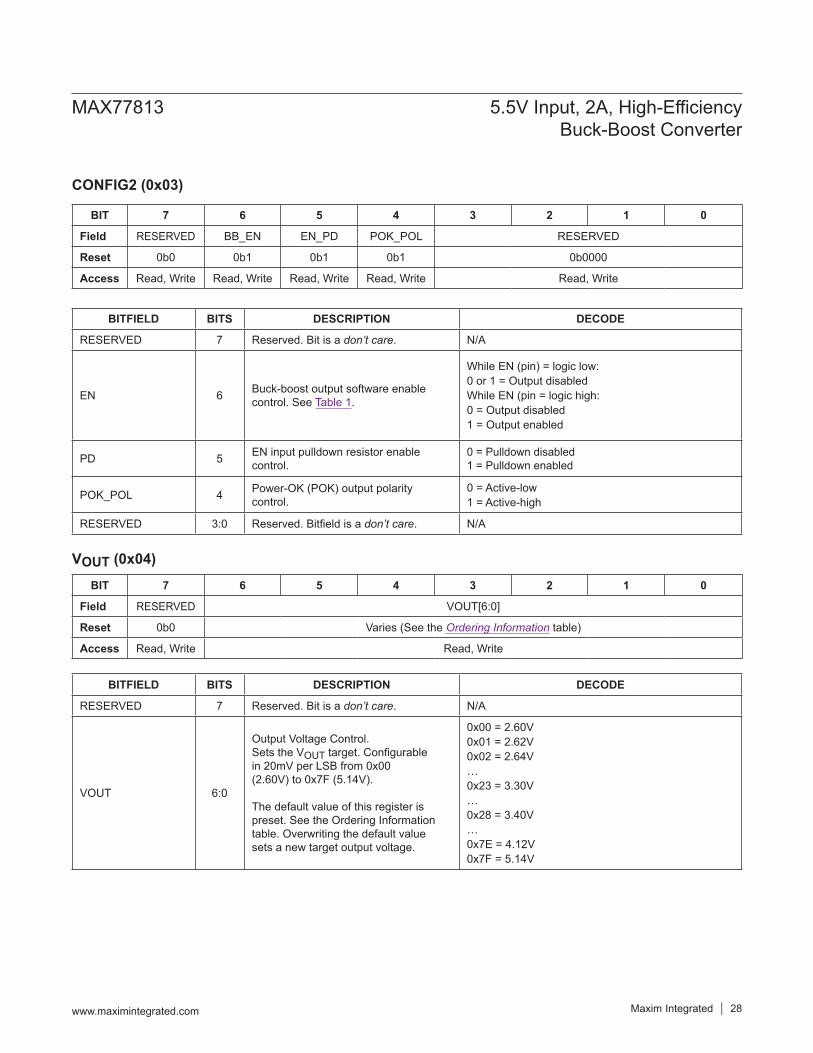
VOUT (0x04)
BIT 7 6 5 4 3 2 1 0
Field RESERVED BB_EN EN_PD POK_POL RESERVED
Reset 0b0 0b1 0b1 0b1 0b0000
Access Read, Write Read, Write Read, Write Read, Write Read, Write
BIT 7 6 5 4 3 2 1 0
Field RESERVED VOUT[6:0]
Reset 0b0 Varies (See the Ordering Information table)
Access Read, Write Read, Write
BITFIELD BITS DESCRIPTION DECODE
RESERVED 7 Reserved. Bit is a don’t care. N/A
EN 6 Buck-boost output software enable control. See Table 1.
While EN (pin) = logic low: 0 or 1 = Output disabled While EN (pin = logic high: 0 = Output disabled 1 = Output enabled
PD 5 EN input pulldown resistor enable control.
0 = Pulldown disabled1 = Pulldown enabled
POK_POL 4 Power-OK (POK) output polarity control.
0 = Active-low1 = Active-high
RESERVED 3:0 Reserved. Bitfield is a don’t care. N/A
BITFIELD BITS DESCRIPTION DECODE
RESERVED 7 Reserved. Bit is a don’t care. N/A
VOUT 6:0
Output Voltage Control. Sets the VOUT target. Configurable in 20mV per LSB from 0x00 (2.60V) to 0x7F (5.14V).
The default value of this register is preset. See the Ordering Information table. Overwriting the default value sets a new target output voltage.
0x00 = 2.60V 0x01 = 2.62V 0x02 = 2.64V … 0x23 = 3.30V … 0x28 = 3.40V … 0x7E = 4.12V 0x7F = 5.14V
CONFIG2 (0x03)
MAX77813 5.5V Input, 2A, High-Efficiency Buck-Boost Converter
www.maximintegrated.com Maxim Integrated 28
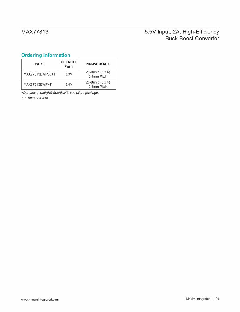
+Denotes a lead(Pb)-free/RoHS-compliant package.T = Tape and reel.
PART DEFAULT VOUT
PIN-PACKAGE
MAX77813EWP33+T 3.3V 20-Bump (5 x 4) 0.4mm Pitch
MAX77813EWP+T 3.4V 20-Bump (5 x 4) 0.4mm Pitch
MAX77813 5.5V Input, 2A, High-Efficiency Buck-Boost Converter
www.maximintegrated.com Maxim Integrated 29
Ordering Information
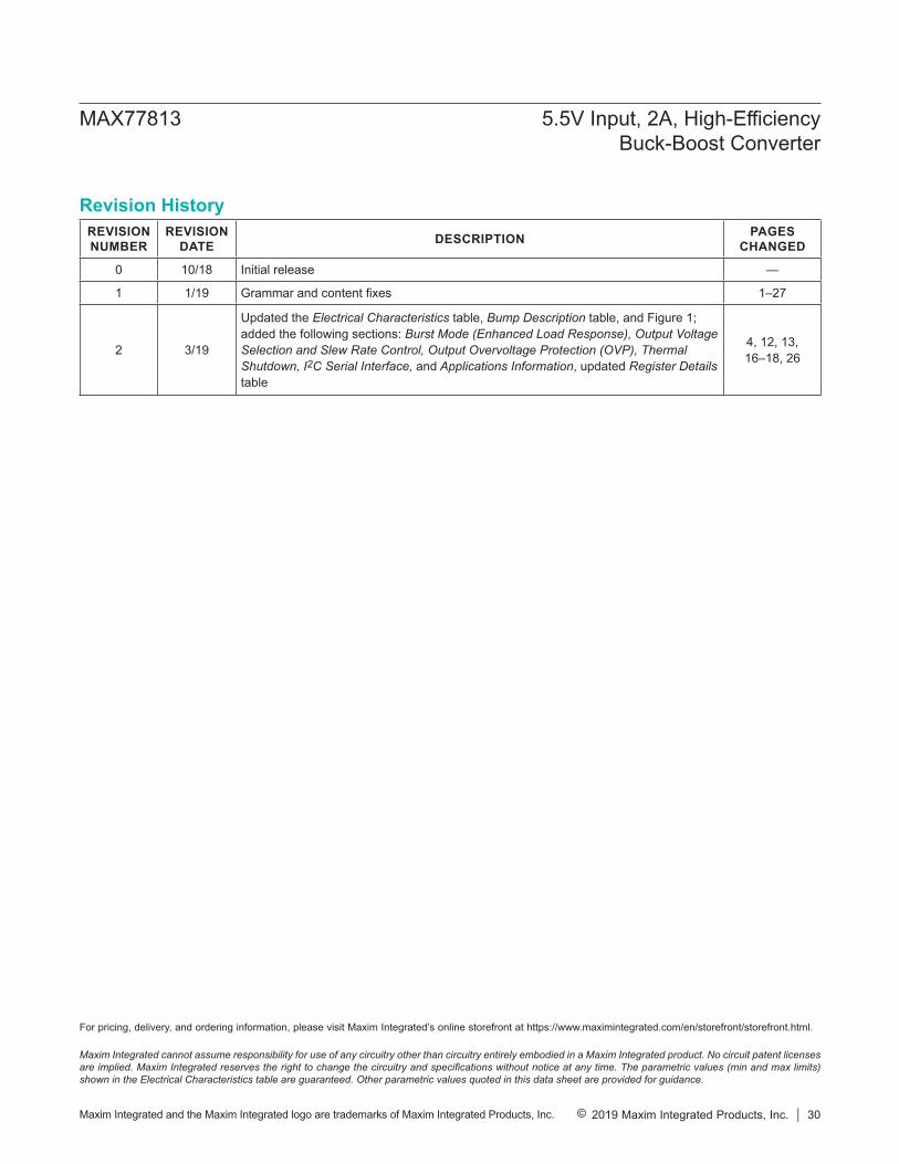
REVISIONNUMBER
REVISIONDATE DESCRIPTION PAGES
CHANGED
0 10/18 Initial release —
1 1/19 Grammar and content fixes 1–27
2 3/19
Updated the Electrical Characteristics table, Bump Description table, and Figure 1; added the following sections: Burst Mode (Enhanced Load Response), Output Voltage Selection and Slew Rate Control, Output Overvoltage Protection (OVP), Thermal Shutdown, I2C Serial Interface, and Applications Information, updated Register Details table
4, 12, 13, 16–18, 26
Maxim Integrated cannot assume responsibility for use of any circuitry other than circuitry entirely embodied in a Maxim Integrated product. No circuit patent licenses are implied. Maxim Integrated reserves the right to change the circuitry and specifications without notice at any time. The parametric values (min and max limits) shown in the Electrical Characteristics table are guaranteed. Other parametric values quoted in this data sheet are provided for guidance.
Maxim Integrated and the Maxim Integrated logo are trademarks of Maxim Integrated Products, Inc. © 2019 Maxim Integrated Products, Inc. 30
MAX77813 5.5V Input, 2A, High-Efficiency Buck-Boost Converter
Revision History
For pricing, delivery, and ordering information, please visit Maxim Integrated’s online storefront at https://www.maximintegrated.com/en/storefront/storefront.html.
![Bridgeless Buck-Boost PFC Converter for Multistring LED Driver€¦ · boost converter as a universal PFC converter [6]. In order to address these issues, a buck-boost converter is](https://img.dokumen.tips/doc/110x75/5eaabf2a4ab79d1e774f9005/bridgeless-buck-boost-pfc-converter-for-multistring-led-driver-boost-converter-as.jpg)