Embed Size (px)
Citation preview
_______________________________________________________________ Maxim Integrated Products 1
For pricing, delivery, and ordering information, please contact Maxim Direct at 1-888-629-4642, or visit Maxim’s website at www.maxim-ic.com.
MAX17019N Evaluation Kit
Eva
lua
tes: M
AX
17
01
919-5936; Rev 0; 6/11
General DescriptionThe MAX17019N evaluation kit (EV kit) demonstrates the MAX17019’s standard application circuit. This quad- output converter steps down high-voltage batteries and/or AC adapters, generating main supplies for ultra-mobile PCs (UMPCs).
The EV kit provides a 5V main stage output voltage (VOUTA), a 1.8V VDDQ output voltage (VOUTB), a 1.05V chipset supply output voltage (VOUTC), and a 0.9V VTT output voltage (VOUTD) from a 6V to 38V battery input range. It delivers up to 4A output current for the 5V out-put, 2.5A for the 1.8V output, 4A for the 1.05V output, and 2A for the 0.9V output. The 1.8V VDDQ and 0.9V VTT are for DDR2 memory applications. All outputs are adjust-able by changing feedback resistors R5–R10.
The IC also has an internal fixed 5V linear regulator capable of supplying 50mA. The EV kit operates at 0.5MHz (VOUTA and VOUTC) and at 1MHz switching frequency (VOUTB). The EV kit has superior line- and load-transient response.
This EV kit is a fully assembled and tested circuit board. It also allows the evaluation of other fixed output voltages by changing R5–R10 resistors.
FeaturesS 6V to 38V Input Range
S Internal 5V Linear Regulator with 50mA Load Capability
S Output Voltages
VOUTA: 5V Up to 4A (Adjustable from 1V to 5.3V)
VOUTB: 1.8V Up to 2.5A (Adjustable from 0.75V to 4V)
VOUTC: 1.05V Up to 4A (Adjustable from 0.75V to 4V)
VOUTD: 0.9V Up to 2A (Adjustable from 0.5V to 2V)
S 0.5MHz Switching Frequency (5V and 1.05V Outputs)
S 1MHz Switching Frequency (1.8V Output)
S Independent Enable Inputs and Power-Good Outputs
S Overvoltage and Undervoltage Fault Protection
S Thermal Fault Protection
S Proven PCB Layout
S Fully Assembled and Tested
Ordering Information
+Denotes lead(Pb)-free and RoHS compliant.
Component List
PART TYPE
MAX17019NEVKIT+ EV Kit
DESIGNATION QTY DESCRIPTION
C1, C2 2
4.7FF Q10%, 50V X7R ceramiccapacitors (1210)Murata GRM32ER71H475KAVX 12105C475KAT2A
C3 122FF, 50V aluminum electrolyticcapacitor (6.3mm x 6.0mm DxL)SANYO 50CE22KX
C4, C11, C20, C24
4
4.7FF Q10% 6.3V X5R ceramiccapacitors (0603)Murata GRM188R60J475KTDK C1608X5R0J475K
DESIGNATION QTY DESCRIPTION
C5, C25, C33 3
1FF Q10%, 6.3V X5R ceramiccapacitors (0402)Murata GRM155R60J105KTDK C1005X5R0J105K
C6 11FF Q10%, 50V X7R ceramiccapacitor (0805)Murata GRM21BR71H105K
C7, C17, C21, C29
4
0.1FF Q10%, 10V X5R ceramiccapacitors (0402)Murata GRM155R60J104KTDK C1005X5R1A104K
MAX17019N Evaluation Kit
Eva
lua
tes:
M
AX
17
01
9
2 ______________________________________________________________________________________
Component List (continued)DESIGNATION QTY DESCRIPTION
C9 1
150FF, 6.3V low-ESR capacitor(B case)SANYO 6TPE150MAZBNEC TOKIN PSLB0J157M(35)
C10, C32, C35 0 Not installed, capacitors (B case)
C14 1
680pF Q10%, 50V X7R ceramiccapacitor (0402)Murata GRM155R71H681KTDK C1005X7R1H681K
C15, C36, C37 0 Not installed, capacitors (0805)
C16, C26, C34 3
10FF Q20%, 6.3V X5R ceramiccapacitors (0805)Murata GRM21BR60J106MTDK C2012X5R0J106M
C18, C30 2
1000pF Q10%, 50V X7R ceramiccapacitors (0402)Murata GRM155R71H102KTDK C1005X7R1H102K
C19, C22 2
330FF, 2.5V low-ESR capacitors(B case)SANYO 2TPE330MAFGBNEC TOKIN PSLB20E337M(18)
C23 1
2200pF Q10%, 50V X7R ceramiccapacitor (0402)Murata GRM155R71H222KTDK C1005X7R1H222K
C27, C28 2
22FF, 6.3V X5R ceramiccapacitors (0805)TDK C2012X5R0J226MTTaiyo Yuden JMK212BJ226MG
C31 1
0.22FF Q10%, 10V X5R ceramiccapacitor (0402)Murata GRM155R60J224KTDK C1005X5R0J224K
DESIGNATION QTY DESCRIPTION
D1 1250mA, 50V Schottky diode (SOT323)Central Semi CMSSH-3E
L1 14.7FH, 7A, 20mI inductor(7mm x 7mm x 4mm)Würth 744311470
L2, L3 2
1FH, 6.8A, 14.2mI inductors(5.8mm x 6.2mm x 3.0mm)NEC TOKIN MPLC0525L1R0TOKO FDV0530-1R0M
N1-A, N1-B 1Dual n-channel MOSFETs (8 SO)Fairchild FDS6982AS
POKA–POKD, REFIND,
SYNC, VTTR7 Test points
R1 1 10I Q5% resistor (0402)
R2, R21 2 0I Q5% resistors (0402)
R3, R4, R20, R24, R29
0 Not installed, resistors (0402)
R5 1 40.2kI Q1% resistor (0402)
R6, R8, R10, R22, R23
5 10kI Q1% resistors (0402)
R7 1 14kI Q1% resistor (0402)
R9 1 4.02kI Q1% resistor (0402)
R11–R19 9 100kI Q5% resistors (0402)
R25 1 51I Q5% resistor (0402)
R26 10.004I Q1%, 1/4W resistor (1206)Vishay (Dale) WSL12064L000FEA
R27, R28 0Not installed, resistors—short (PC trace) (0612)
SW1 15-position, low-profile DIP switchITT SD05H0SB or Equivalent
U1 1Quad output controller(48 TQFN-EP)Maxim MAX17019ATM+
— 1PCB: MAX17019N EVALUATION KIT+
MAX17019N Evaluation Kit
Eva
lua
tes: M
AX
17
01
9
_______________________________________________________________________________________ 3
Quick Start Required Equipment
• MAX17019N EV kit
• 6V to 38V, 100W DC power supply
• Four dummy loads capable of sinking 4A each
• Four digital multimeters
• 100MHz dual-trace oscilloscope
ProcedureThe EV kit is a fully assembled and tested surface-mount board. Follow the steps below to verify board operation. Caution: Do not turn on the power supply until all connections are completed.
1) Ensure that the circuit is connected correctly to the power supply and dummy loads prior to applying any power.
2) Set SW1 (1, 10) to the on position (SHDN = VBATT, IC enabled).
Set SW1 (2, 9) to the on position (ONA = VDD, VOUTA enabled).
Set SW1 (3, 8) to the on position (ONB = VDD, VOUTB enabled).
Set SW1 (4, 7) to the on position (ONC = VDD, VOUTC enabled).
Set SW1 (5, 6) to the on position (OND = VDD, VOUTD enabled).
3) Connect the first DMM across the VOUTA and GND PCB pads.
Connect the second DMM across the VOUTB and GND PCB pads.
Connect the third DMM across the VOUTC and GND PCB pads.
Connect the fourth DMM across the VOUTD and GND PCB pads.
4) Turn on the power supply and adjust the input volt-age to 12V.
5) Verify that the output voltages are VOUTA = 5V, VOUTB = 1.8V, VOUTC = 1.05V, and VOUTD = 0.9V.
Detailed Description of Hardware5V Output-Voltage Setting (VOUTA)
The MAX17019N EV kit is shipped with FBA connected to resistors R5 and R6, which sets the VOUTA voltage to 5V.
To change the output voltage to a value between 1V and 5.3V, remove R5. Calculate R5 using the following equation:
R5 = R6 [(VOUTA/VFBA) - 1]
where VFBA = 1V and R6 =10kI Q1%. For an output voltage of 1V, place a short across R5 and leave R6 open.
Note: Indicate that you are using the MAX17019 when contacting these component suppliers.
Component SuppliersSUPPLIER PHONE WEBSITE
AVX Corporation 843-946-0238 www.avx.com
Central Semiconductor Corp. 631-435-1110 www.centralsemi.com
Fairchild Semiconductor 888-522-5372 www.fairchildsemi.com
Murata Manufacturing Co., Ltd. 770-436-1300 www.murata.com
NEC TOKIN America, Inc. 408-324-1790 www.nec-tokinamerica.com
SANYO Electric Company, Ltd. 619-661-6835 www.sanyodevice.com
Taiyo Yuden 800-348-2496 www.t-yuden.com
TDK Corp. 847-803-6100 www.component.tdk.com
TOKO America, Inc. 847-297-0070 www.tokoam.com
Vishay 402-564-3131 www.vishay.com
Würth Electronik GmbH & Co. KG 201-785-8800 www.we-online.com
MAX17019N Evaluation Kit
Eva
lua
tes:
M
AX
17
01
9
4 ______________________________________________________________________________________
1.8V Output-Voltage Setting (VOUTB)The EV kit is shipped with FBB connected to resistors R7 and R8, which sets the VOUTB voltage to 1.8V.
To change the output voltage to a value between 0.75V and 4V, remove R7. Calculate R7 using the following equation:
R7 = R8 [(VOUTB/VFBB) - 1]
where VFBB = 0.75V and R8 =10kI Q1%. For an output voltage of 0.75V, place a short across R7 and leave R8 open.
1.05V Output-Voltage Setting (VOUTC)The EV kit is shipped with FBC connected to resistors R9 and R10, which sets the VOUTC voltage to 1.05V.
To change the output voltage to a value between 0.75V and 4V, remove R9. Calculate R9 using the following equation:
R9 = R10 [(VOUTC/VFBC) - 1]
where VFBC = 0.75V and R10 =10kI Q1%. For an output voltage of 0.75V, place a short across R9 and leave R10 open.
0.9V Output-Voltage Setting (VOUTD)The EV kit is shipped with FBD connected directly to output voltage VOUTD. The voltage at FBD tracks the REFIND voltage. The REFIND voltage is set to 0.9V (half the output voltage at VOUTB) by resistor-divider R22 and R23.
To change the VOUTD output voltage to a value between 0.5V and 2V, remove R22. Calculate R22 using the fol-lowing equation:
R22 = R23 [(VOUTB/VOUTD) - 1]
where R23 =10kI Q1%.
Frequency Selection (FREQ)The switching frequency of the EV kit can be adjusted by removing resistor R24 and installing a short across resistors R20 or R21. As configured, the EV kit operates at 0.5MHz (VOUTA and VOUTC) and at 1MHz switch-ing frequency (VOUTB). When changing the switching frequency, refer to the MAX17019 IC data sheet for the proper component selections and calculations for the inductors and output capacitors.
Table 1. Switch SW1 Settings
Table 2. Switching-Frequency Selection
Note: As configured, the MAX17019N EV kit is shipped with all SW1 settings in the off position.
*Default position.
SW1 PIN CONTROL IC OUTPUT
SW1-AOff SHDN pin is connected to GND Shutdown mode (all outputs disabled)
On SHDN pin is connected to VBATT IC enabled (all outputs depend on SW1 position settings)
SW1-BOff ONA pin is connected to GND Disables VOUTA, VOUTA = 0V
On ONA pin is connected to VDD Enables VOUTA, VOUTA = 5V
SW1-COff ONB pin is connected to GND Disables VOUTB, VOUTB = 0V
On ONB pin is connected to VDD Enables VOUTB, VOUTB = 1.8V
SW1-DOff ONC pin is connected to GND Disables VOUTC, VOUTC = 0V
On ONC pin is connected to VDD Enables VOUTC, VOUTC = 1.05V
SW1-EOff OND pin is connected to GND Disables VOUTD, VOUTD = 0V
On OND pin is connected to VDD Enables VOUTD, VOUTD = 0.9V
FREQ PINSWITCHING FREQUENCY
VOUTA VOUTB VOUTC
Connected to VDD through open resistor R24 250kHz 500kHz 250kHz
Connected to REF through open resistor R20 375kHz 750kHz 375kHz
Connected to GND through 0I resistor R21* 500kHz 1MHz 500kHz
MAX17019N Evaluation Kit
Eva
lua
tes: M
AX
17
01
9
_______________________________________________________________________________________ 5
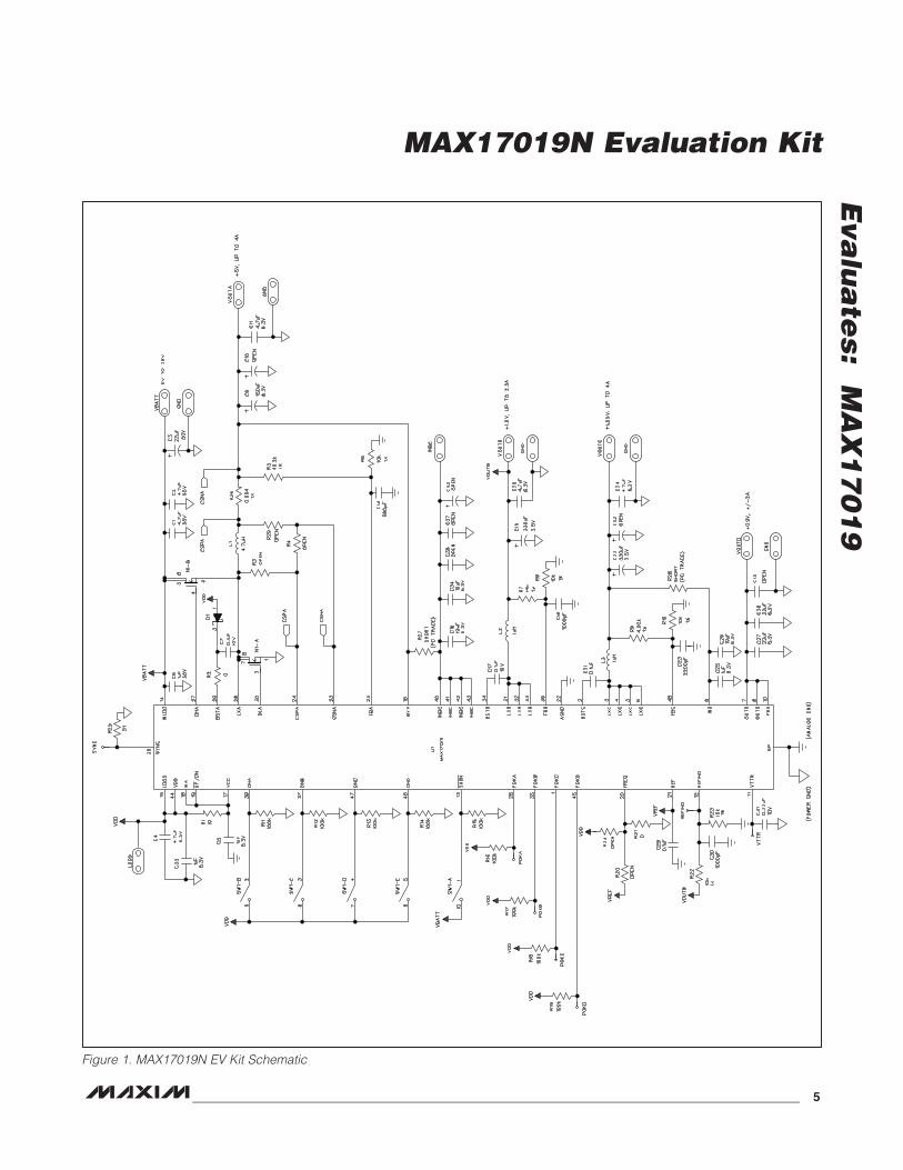
Figure 1. MAX17019N EV Kit Schematic
MAX17019N Evaluation Kit
Eva
lua
tes:
M
AX
17
01
9
6 ______________________________________________________________________________________
Figure 4. MAX17019N EV Kit PCB Layout—Layer 2
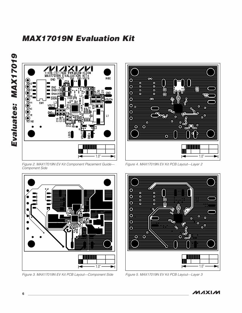
Figure 5. MAX17019N EV Kit PCB Layout—Layer 3Figure 3. MAX17019N EV Kit PCB Layout—Component Side
Figure 2. MAX17019N EV Kit Component Placement Guide—Component Side
1.0” 1.0”
1.0”1.0”
MAX17019N Evaluation Kit
Eva
lua
tes: M
AX
17
01
9
_______________________________________________________________________________________ 7
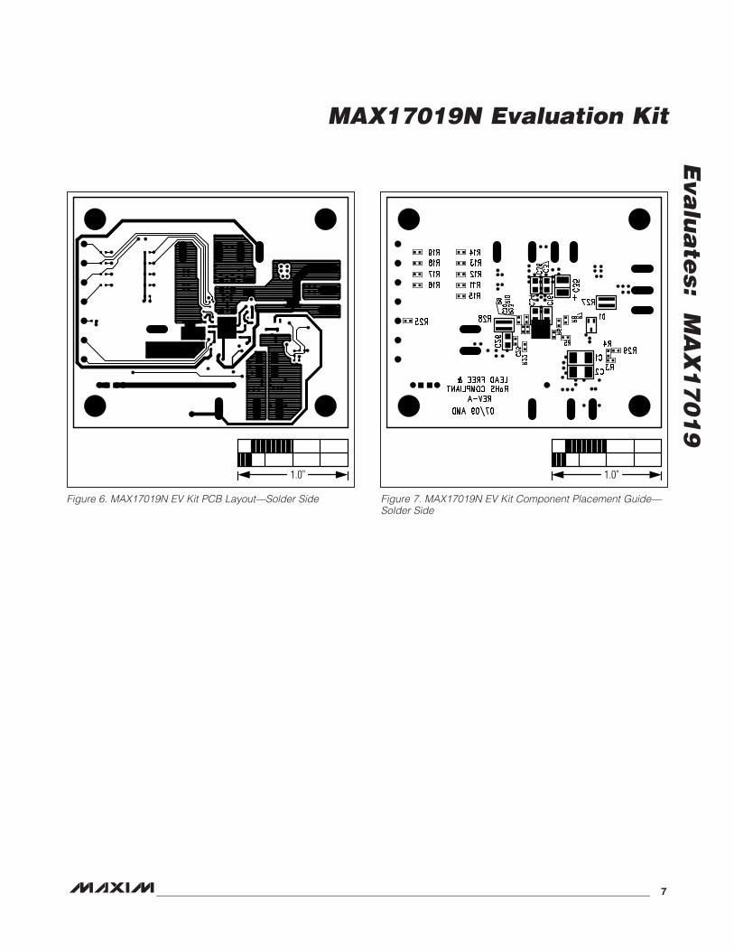
Figure 6. MAX17019N EV Kit PCB Layout—Solder Side Figure 7. MAX17019N EV Kit Component Placement Guide—Solder Side
1.0” 1.0”
Maxim cannot assume responsibility for use of any circuitry other than circuitry entirely embodied in a Maxim product. No circuit patent licenses are implied. Maxim reserves the right to change the circuitry and specifications without notice at any time.
8 Maxim Integrated Products, 120 San Gabriel Drive, Sunnyvale, CA 94086 408-737-7600© 2011 Maxim Integrated Products Maxim is a registered trademark of Maxim Integrated Products, Inc.
MAX17019N Evaluation Kit
Eva
lua
tes:
M
AX
17
01
9 Revision History
REVISIONNUMBER
REVISIONDATE
DESCRIPTIONPAGES
CHANGED
0 6/11 Initial release —
![USER MANUAL - HP HEAVEN1].16.pdf750 mm 5mm ID Silicon hose Connect solenoid 4 Large spring hose clamps Use on 5mm ID Silicon hose 2 5 – 6.3mm hose reducer Reduce 6.3mm hose to 5mm](https://img.dokumen.tips/doc/110x75/5fe6e7604b82bd6017103ec8/user-manual-hp-116pdf-750-mm-5mm-id-silicon-hose-connect-solenoid-4-large-spring.jpg)