Embed Size (px)
Citation preview
Evaluates: MAX14940/MAX14943/MAX14946/MAX14949
MAX149X2 Evaluation Kit
General DescriptionThe MAX149X2 evaluation kit (EV kit) is a fully assembled and tested PCB that demonstrates the functionality of the MAX14943 isolated RS-485/PROFIBUS transceiver. The EV kit operates from a single 3.3V supply and features an on-board isolated power supply to power the secondary-side of the circuit.The MAX149X2 EV kit comes with the MAX14943GWE+ installed, but can also be used to evaluate the pin-compatible MAX14940, MAX14946, and MAX14949 ICs.
Features ● Operates from a Single 3.3V Supply ● Terminal Block Connectors for Easy RS-485/
PROFIBUS Evaluation ● 5000VRMS Isolation for 60s ● Fully Assembled and Tested ● Proven PCB Layout
19-7646; Rev 0; 6/15
Ordering Information appears at end of data sheet.
Quick StartRequired Equipment
● MAX149X2 EV kit ● 3.3V, 1A DC power supply ● Signal/function generator ● Oscilloscope
Startup ProcedureThe EV kit is fully assembled and tested. Follow the steps below to verify board operation:1) Set the DC power supply to 3.3V and connect the
DC power supply between the EV kits VDDA and GNDA connectors of the EV kit.
2) Ensure that J2 and J3 are in their default positions (see Table 1).
3) Turn on the power supply.4) Set the signal/function generator to output a 100kHz
0 to 3V square wave. Note: Set the signal/function generator to operate with a high-impedance load. If needed, the R1 pad is available to add a 50Ω impedance to ground.
5) Connect the signal/function generator to the TXD test point.
6) Verify that the A and B outputs switch as the signal toggles.
Table 1. Jumper Settings (J1–J6)JUMPER SHUNT POSITION DESCRIPTION
J11-2 Receiver is disabled. RXD is high impedance.
2-3* Receiver is enabled. RXD is active.
J21-2* Driver is enabled. DEM is high.
2-3 Driver is disabled. DEM is low.
J3Open* DE and RE are not connected together.
Closed DE and RE are connected together.
J4Open* A and B are not connected through the on-board 120Ω resistor.
Closed Connects the on-board 120Ω resistor between A and B.
*Default position.
Maxim Integrated │ 2www.maximintegrated.com
Evaluates: MAX14940/MAX14943/ MAX14946/MAX14949
MAX149X2 Evaluation Kit
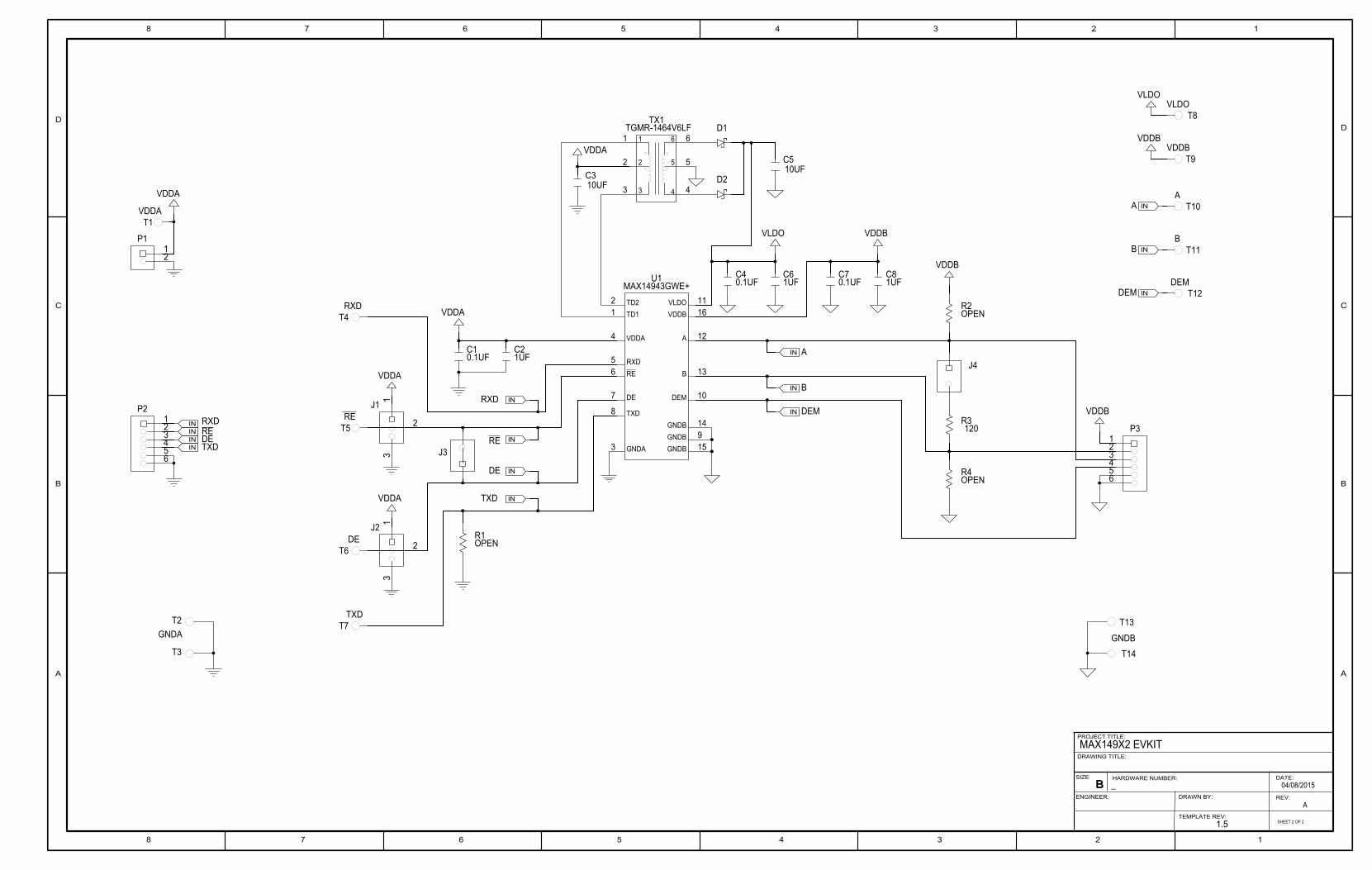
Detailed Description of HardwareThe MAX149X2 EV kit is a fully assembled and tested circuit board for evaluating the MAX14943 isolated RS-485/Profibus transceiver (U1). The EV kit has been designed to allow for evaluating the IC alone or in a standard RS-485 configuration. The EV kit is powered from a single 3.3V power supply.
External Power SupplyThe power on the EV kit is derived from a single 3.3V source. Connect an external supply from GNDA to either the VDDA test point or P1 connector to supply the 3.3V to the logic side (A) of the circuit. The integrated push-pull transformer driver and external transformer (TX1) generate an isolated supply for powering the (B) isolated side of the board.
Evaluating the Isolated RS-485 InterfaceDriver and Receiver Enable SelectionThe EV kit features three jumpers (J1, J2, and J3) to enable/disable the driver and receiver outputs. Set J1 to 2-3 to enable the receiver. Set J2 to 1-2 to enable the driver. To actively control both enables, remove J1 and J2 and close J3, which connects DE and RE together.
Resistors R2 – R4 ConfigurationFor end-of-the-line transceivers, close J4 to connect a 120Ω resistor (R3) between the A and B RS-485 I/Os on the IC. Pullup and pulldown resistors are generally used on the receiver inputs to guarantee a known state in the event that all nodes on the bus are in receive mode, or the cable becomes disconnected. The exact value for these resistors varies with the application. Pads are provided for pullup (R2) and pulldown (R4) resistors for the A-B lines, although the use of these resistors is purely optional. Note that the MAX14943 features true fail-safe receiver inputs that ensure RXD is high when the receiver inputs are shorted, open, or connected to an idle bus.
Selecting a TransformerTable 2 is a list of transformers designed to operate with the device family. Select the transformer that best meets the performance requirements of the end application. All transformers in Table 2 can be used on the EV kit.
Table 2. Transformer Selection
MANUFACTURER/PART NUMBER TURNS RATIO ISOLATION VOLTAGE (VRMS)
A-SIDE SUPPLY (V)
CAN BE USED WITH MAXIM PART NUMBERS
HALO TGMS-1440V6LF 1CT: 1.33CT 2750 5V MAX14940, MAX14946
HALO TGMS-1464V6LF 1CT:2.4CT 2750 3.3V MAX14940, MAX14946
HALO TGMR-1440V6LF 1CT:1.33CT 5000 5V MAX14943, MAX14949
HALO TGMR-1464V6LF 1CT:2.4CT 5000 3.3V MAX14943, MAX14949
WURTH 750315226 1CT:1.3CT 2750 5V MAX14940, MAX14946
WURTH 750315228 1CT: 2CT 2750 3.3V MAX14940, MAX14946
WURTH 750315230 1CT:1.3CT 5000 5V MAX14943, MAX14949
WURTH 750315232 1CT: 2CT 5000 3.3V MAX14943, MAX14949
Maxim Integrated │ 3www.maximintegrated.com
Evaluates: MAX14940/MAX14943/ MAX14946/MAX14949
MAX149X2 Evaluation Kit
Ordering InformationPART TYPE
MAX149X2EVKIT# EV Kit
#Denotes RoHS compliant.
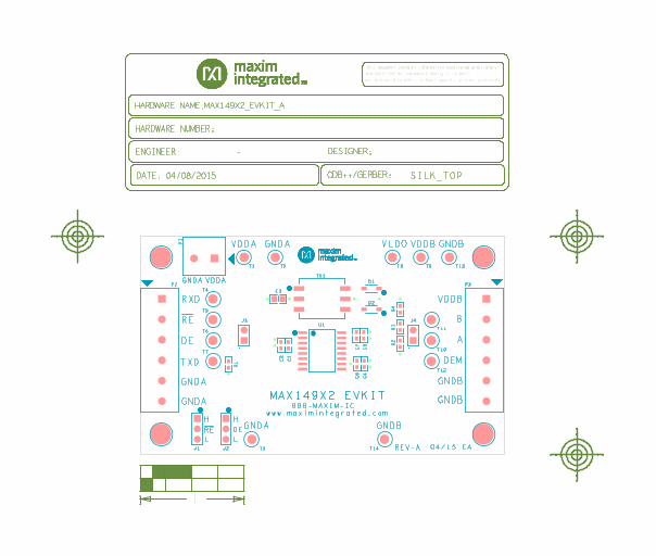
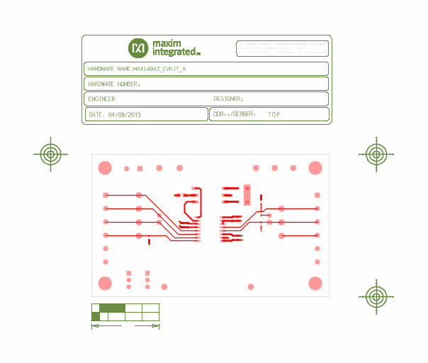
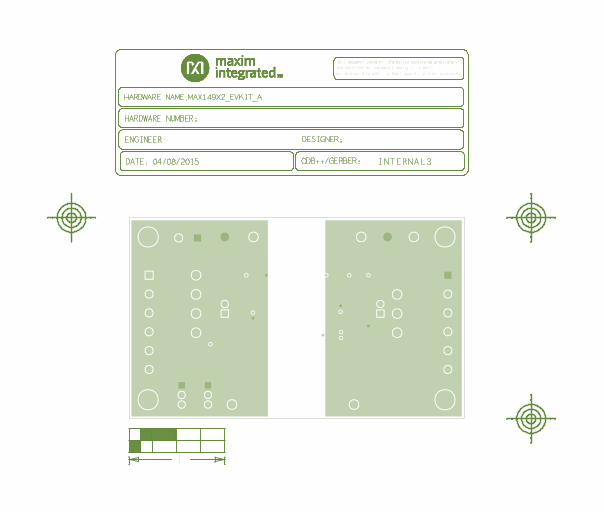
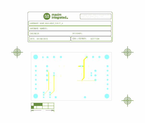
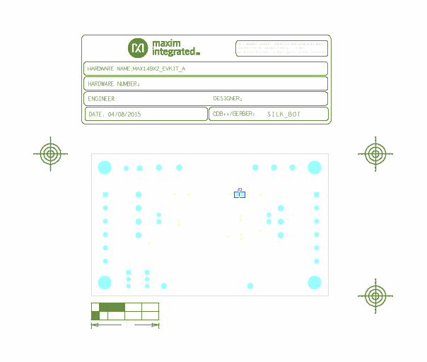
Component List, PCB Layout, and SchematicSee the following links for component information, PCB layout diagrams, and schematics:
● MAX149X2 EV BOM ● MAX149X2 EV PCB Layout ● MAX149X2 EV Schematic
Maxim Integrated cannot assume responsibility for use of any circuitry other than circuitry entirely embodied in a Maxim Integrated product. No circuit patent licenses are implied. Maxim Integrated reserves the right to change the circuitry and specifications without notice at any time.
Maxim Integrated and the Maxim Integrated logo are trademarks of Maxim Integrated Products, Inc. © 2015 Maxim Integrated Products, Inc. │ 4
Evaluates: MAX14940/MAX14943/ MAX14946/MAX14949
MAX149X2 Evaluation Kit
Revision HistoryREVISIONNUMBER
REVISIONDATE DESCRIPTION PAGES
CHANGED0 6/15 Initial release —
For pricing, delivery, and ordering information, please contact Maxim Direct at 1-888-629-4642, or visit Maxim Integrated’s website at www.maximintegrated.com.
SHEET 2 OF 2
_
MAX149X2 EVKIT
A
04/08/2015
1.5
10UF
10UF
TGMR-1464V6LF
0.1UF
OPEN
RXD
DEM
1UF
GNDB
1UF
TXD
GNDA
RE
DE
0.1UF 1UF
A
VDDB
B
0.1UF
120
OPEN
VLDO
OPEN
VDDA
MAX14943GWE+
D2
D1
C5
R2
R4
J3
C3
P3
P2
P1
R3
TX1
T12
T10
T11
T9
T8
T1
T13
T14T3
T2
J4
T7
R1J2
T6
T5
T4
J1
C8C6
C2
C7C4
C1
U1
VDDA
VLDO VDDB
VDDA
TXDDE
VDDA
RE
RXD
VDDA
DEM
B
VDDB
B
A
DEM VDDB
VDDB
VLDO
RXDRE
DE
TXD
AVDDA
654321
654321
21
6
5
43
2
1
3
2
13
2
1
1116
4
8
21
5
15914
3
107
13
12
6
6
5
43
2
1
IN
IN
IN
IN
IN
IN
IN
IN
IN
IN
ININININ
VLDO
A
B
DEM
GNDBGNDBGNDB
GNDA
TXD
DE
RERXD
TD1TD2
VDDB
VDDA
DRAWN BY:
TEMPLATE REV:
REV:
2
B
D
1
C
A
2345
345
678
C
B
A
8 7 6 1
D
DATE:
PROJECT TITLE:
DRAWING TITLE:
SIZE HARDWARE NUMBER:
ENGINEER:
BB
T13
P3
B
A
GNDB
T9
VDDB
T11
DEM
T10
GNDB
T12
GNDB
04/15 EA
SILK_TOP
VDDB
T8
J4
R4
R3
R2
REV-A
and shall not be reproduced wholly or in part,
This document contains information considered proprietary,
nor disclosed to others without specific written permission.
VLDO
D1
D2
C8
C7
C4
C6
GNDB
T14
ODB++/GERBER:
TX1
U1
888-MAXIM-IC
GNDA
T2
C3
C2
C1
www.maximintegrated.com
MAX149X2 EVKIT
T3
VDDA
T1
J3
R1
H
DE
L
GNDA
VDDA
T4
T5
T6
T7
H
RE
L
J2
04/08/2015P1
GNDA
RXD
P2
RE
DE
TXD
GNDA
GNDA
J1
1"
HARDWARE NAME:MAX149X2_EVKIT_A
HARDWARE NUMBER:
DATE:
TOP
and shall not be reproduced wholly or in part,
This document contains information considered proprietary,
nor disclosed to others without specific written permission.
ODB++/GERBER:04/08/2015
1"
HARDWARE NAME:MAX149X2_EVKIT_A
HARDWARE NUMBER:
DATE:

INTERNAL2
and shall not be reproduced wholly or in part,
This document contains information considered proprietary,
nor disclosed to others without specific written permission.
ODB++/GERBER:04/08/2015
1"
HARDWARE NAME:MAX149X2_EVKIT_A
HARDWARE NUMBER:
DATE:
INTERNAL3
and shall not be reproduced wholly or in part,
This document contains information considered proprietary,
nor disclosed to others without specific written permission.
ODB++/GERBER:04/08/2015
1"
HARDWARE NAME:MAX149X2_EVKIT_A
HARDWARE NUMBER:
DATE:
BOTTOM
and shall not be reproduced wholly or in part,
This document contains information considered proprietary,
nor disclosed to others without specific written permission.
ODB++/GERBER:04/08/2015
1"
HARDWARE NAME:MAX149X2_EVKIT_A
HARDWARE NUMBER:
DATE:
SILK_BOT
and shall not be reproduced wholly or in part,
This document contains information considered proprietary,
nor disclosed to others without specific written permission.
C5
ODB++/GERBER:04/08/2015
1"
HARDWARE NAME:MAX149X2_EVKIT_A
HARDWARE NUMBER:
DATE:
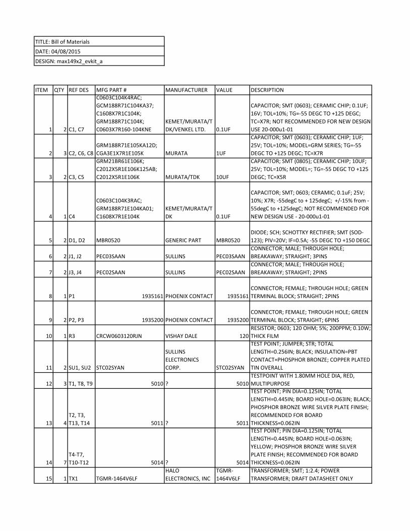
ITEM QTY REF DES MFG PART # MANUFACTURER VALUE DESCRIPTION
1 2 C1, C7
C0603C104K4RAC; GCM188R71C104KA37; C1608X7R1C104K; GRM188R71C104K; C0603X7R160-104KNE
KEMET/MURATA/TDK/VENKEL LTD. 0.1UF
CAPACITOR; SMT (0603); CERAMIC CHIP; 0.1UF; 16V; TOL=10%; TG=-55 DEGC TO +125 DEGC; TC=X7R; NOT RECOMMENDED FOR NEW DESIGN USE 20-000u1-01
2 3 C2, C6, C8GRM188R71E105KA12D; CGA3E1X7R1E105K MURATA 1UF
CAPACITOR; SMT (0603); CERAMIC CHIP; 1UF; 25V; TOL=10%; MODEL=GRM SERIES; TG=-55 DEGC TO +125 DEGC; TC=X7R
3 2 C3, C5
GRM21BR61E106K; C2012X5R1E106K125AB; C2012X5R1E106K MURATA/TDK 10UF
CAPACITOR; SMT (0805); CERAMIC CHIP; 10UF; 25V; TOL=10%; MODEL=; TG=-55 DEGC TO +125 DEGC; TC=X5R
4 1 C4
C0603C104K3RAC; GRM188R71E104KA01; C1608X7R1E104K
KEMET/MURATA/TDK 0.1UF
CAPACITOR; SMT; 0603; CERAMIC; 0.1uF; 25V; 10%; X7R; -55degC to + 125degC; +/-15% from -55degC to +125degC; NOT RECOMMENDED FOR NEW DESIGN USE - 20-000u1-01
5 2 D1, D2 MBR0520 GENERIC PART MBR0520DIODE; SCH; SCHOTTKY RECTIFIER; SMT (SOD-123); PIV=20V; IF=0.5A; -55 DEGC TO +150 DEGC
6 2 J1, J2 PEC03SAAN SULLINS PEC03SAANCONNECTOR; MALE; THROUGH HOLE; BREAKAWAY; STRAIGHT; 3PINS
7 2 J3, J4 PEC02SAAN SULLINS PEC02SAANCONNECTOR; MALE; THROUGH HOLE; BREAKAWAY; STRAIGHT; 2PINS
8 1 P1 1935161 PHOENIX CONTACT 1935161CONNECTOR; FEMALE; THROUGH HOLE; GREEN TERMINAL BLOCK; STRAIGHT; 2PINS
9 2 P2, P3 1935200 PHOENIX CONTACT 1935200CONNECTOR; FEMALE; THROUGH HOLE; GREEN TERMINAL BLOCK; STRAIGHT; 6PINS
10 1 R3 CRCW0603120RJN VISHAY DALE 120RESISTOR; 0603; 120 OHM; 5%; 200PPM; 0.10W; THICK FILM
11 2 SU1, SU2 STC02SYAN
SULLINS ELECTRONICS CORP. STC02SYAN
TEST POINT; JUMPER; STR; TOTAL LENGTH=0.256IN; BLACK; INSULATION=PBT CONTACT=PHOSPHOR BRONZE; COPPER PLATED TIN OVERALL
12 3 T1, T8, T9 5010 ? 5010TESTPOINT WITH 1.80MM HOLE DIA, RED, MULTIPURPOSE
13 4T2, T3, T13, T14 5011 ? 5011
TEST POINT; PIN DIA=0.125IN; TOTAL LENGTH=0.445IN; BOARD HOLE=0.063IN; BLACK; PHOSPHOR BRONZE WIRE SILVER PLATE FINISH; RECOMMENDED FOR BOARD THICKNESS=0.062IN
14 7T4-T7, T10-T12 5014 ? 5014
TEST POINT; PIN DIA=0.125IN; TOTAL LENGTH=0.445IN; BOARD HOLE=0.063IN; YELLOW; PHOSPHOR BRONZE WIRE SILVER PLATE FINISH; RECOMMENDED FOR BOARD THICKNESS=0.062IN
15 1 TX1 TGMR-1464V6LFHALO ELECTRONICS, INC
TGMR-1464V6LF
TRANSFORMER; SMT; 1:2.4; POWER TRANSFORMER; DRAFT DATASHEET ONLY
TITLE: Bill of Materials
DATE: 04/08/2015
DESIGN: max149x2_evkit_a

16 1 U1 MAX14943GWE+ MAXIMMAX14943GWE+
EVKIT PART-IC; PACKAGE CODE: W16M-9; OUTLINE DRAWING NO.: 21-0042; LAND PATTERN DRAWING NO.: 90-0107; WSOIC16 300MIL
17 1 MAX149x2 MAXIM PCB PCB: MAX149x2
TOTAL 37
ITEM QTY REF DES MFG PART # MANUFACTURER VALUE DESCRIPTION
1 3 R1, R2, R4 N/A N/A OPEN PACKAGE OUTLINE 0603 RESISTOR - EVKIT
TOTAL 3
DO NOT PURCHASE(DNP)