Embed Size (px)
Citation preview

________________________________________________________________ _Maxim Integrated Products_ _ 1
For pricing, delivery, and ordering information, please contact Maxim Direct at 1-888-629-4642, or visit Maxim’s website at www.maxim-ic.com.
MAX11105 Evaluation Kit
Eva
lua
tes: M
AX
11
10
5
General DescriptionThe MAX11105 evaluation kit (EV kit) is a fully assem-bled and tested PCB that evaluates the MAX11105 12-bit, SPIK-compatible, 2Msps, analog-to-digital converter (ADC). The EV kit also includes Windows XPM, Windows VistaM, and WindowsM 7-compatible software that provides a simple graphical user interface (GUI) for exercising the features of the device. The EV kit comes with a MAX11105AUT+ installed in a 6-pin SOT package.
FeaturesS 32MHz_SPI_Interface
S Windows_XP,_Windows_Vista,_and_Windows_7-Compatible_Software
S Time_Domain,_Frequency_Domain,_and_Histogram_Plotting_in_the_EV_Kit_Software
S Frequency,_RMS,_Min,_Max,_and_Average_DC_Calculations_in_the_EV_Kit_Software
S Collects_up_to_1_Mega_Samples
S On-Board_Input_Buffer
S USB-PC_Connection
S Proven_PCB_Layout
S Fully_Assembled_and_Tested
Ordering Information
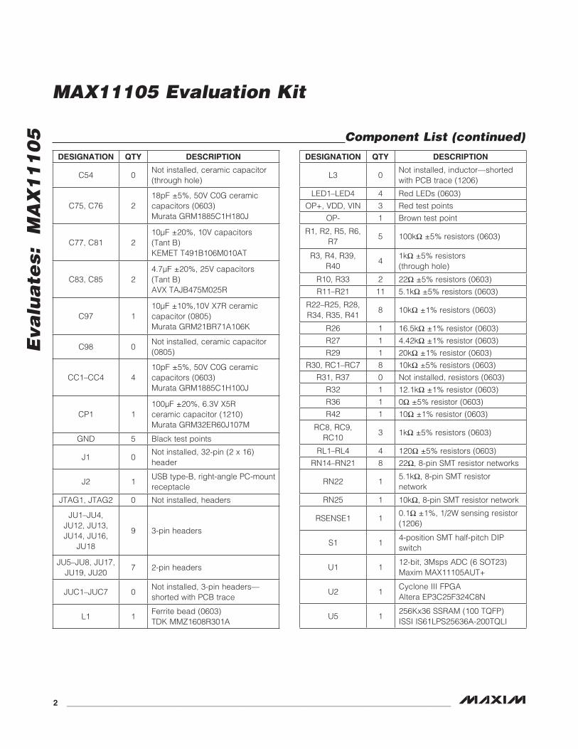
Component List
SPI is a trademark of Motorola, Inc.
+Denotes lead(Pb)-free and RoHS compliant.
Windows, Windows XP, and Windows Vista are registered trademarks of Microsoft Corp.
19-5660; Rev 0; 12/10
PART TYPE
MAX11105EVKIT+ EV Kit
DESIGNATION QTY DESCRIPTION
AIN_AC, AIN_DC, CS, DOUT, SCLK
5 White test points
AIN_AC_SMA, AIN_DC_SMA,
10MHZCLK3 50I SMA female jacks
BUTTON, CPU_RESET,
RECONFIGURE3 Pushbutton switches
C1, C3 21000pF Q10%, 50V X7R ceramic capacitors (0603)Murata GRM188R71H102K
C2, C4, C31, C34, C36, C42,
C43, C47, C55–C72, C78, C79, C80, C82,
C84, C86
320.1FF Q10%, 25V X7R ceramic capacitors (0603)Murata GRM188R71E104K
DESIGNATION QTY DESCRIPTION
C5–C29 250.1FF Q10%, 16V X7R ceramic capacitors (0402)Murata GRM155R71C104K
C30, C95, C96, CB1, CB2, CB3
61FF Q10%, 16V X7R ceramic capacitors (0603)Murata GRM188R71C105K
C32 10.01FF Q10%, 16V X7R ceramic capacitor (0603)Murata GRM188R71C103K
C33, C38, C39, C40
44.7FF Q10%, 6.3V X5R ceramic capacitors (0603)Murata GRM188R60J475K
C35 11FF Q10%, 6.3V C0G ceramic capacitor (0805)Murata GRM21BR70J105K
C37, C41, C44, C45, C46, C48, C73, CP2, CP3
910FF Q10%, 6.3V X5R ceramic capacitors (0603)Murata GRM188R60J106M
C49, C53, C74, C99, C100
0Not installed, ceramic capacitors (0603)
MAX11105 Evaluation Kit
Eva
lua
tes:
M
AX
11
10
5
2_ _ _______________________________________________________________________________________
Component List (continued)
DESIGNATION QTY DESCRIPTION
C54 0Not installed, ceramic capacitor (through hole)
C75, C76 218pF Q5%, 50V C0G ceramic capacitors (0603)Murata GRM1885C1H180J
C77, C81 210FF Q20%, 10V capacitors (Tant B)KEMET T491B106M010AT
C83, C85 24.7FF Q20%, 25V capacitors(Tant B)AVX TAJB475M025R
C97 110FF Q10%,10V X7R ceramic capacitor (0805)Murata GRM21BR71A106K
C98 0Not installed, ceramic capacitor (0805)
CC1–CC4 410pF Q5%, 50V C0G ceramic capacitors (0603)Murata GRM1885C1H100J
CP1 1100FF Q20%, 6.3V X5R ceramic capacitor (1210)Murata GRM32ER60J107M
GND 5 Black test points
J1 0Not installed, 32-pin (2 x 16) header
J2 1USB type-B, right-angle PC-mount receptacle
JTAG1, JTAG2 0 Not installed, headers
JU1–JU4, JU12, JU13, JU14, JU16,
JU18
9 3-pin headers
JU5–JU8, JU17, JU19, JU20
7 2-pin headers
JUC1–JUC7 0Not installed, 3-pin headers—shorted with PCB trace
L1 1Ferrite bead (0603)TDK MMZ1608R301A
DESIGNATION QTY DESCRIPTION
L3 0Not installed, inductor—shorted with PCB trace (1206)
LED1–LED4 4 Red LEDs (0603)
OP+, VDD, VIN 3 Red test points
OP- 1 Brown test point
R1, R2, R5, R6, R7
5 100kI Q5% resistors (0603)
R3, R4, R39, R40
41kI Q5% resistors (through hole)
R10, R33 2 22I Q5% resistors (0603)
R11–R21 11 5.1kI Q5% resistors (0603)
R22–R25, R28, R34, R35, R41
8 10kI Q1% resistors (0603)
R26 1 16.5kI Q1% resistor (0603)
R27 1 4.42kI Q1% resistor (0603)
R29 1 20kI Q1% resistor (0603)
R30, RC1–RC7 8 10kI Q5% resistors (0603)
R31, R37 0 Not installed, resistors (0603)
R32 1 12.1kI Q1% resistor (0603)
R36 1 0I Q5% resistor (0603)
R42 1 10I Q1% resistor (0603)
RC8, RC9, RC10
3 1kI Q5% resistors (0603)
RL1–RL4 4 120I Q5% resistors (0603)
RN14–RN21 8 22I, 8-pin SMT resistor networks
RN22 15.1kI, 8-pin SMT resistor network
RN25 1 10kI, 8-pin SMT resistor network
RSENSE1 10.1I Q1%, 1/2W sensing resistor (1206)
S1 14-position SMT half-pitch DIP switch
U1 112-bit, 3Msps ADC (6 SOT23)Maxim MAX11105AUT+
U2 1Cyclone III FPGAAltera EP3C25F324C8N
U5 1256Kx36 SSRAM (100 TQFP)ISSI IS61LPS25636A-200TQLI
MAX11105 Evaluation Kit
Eva
lua
tes: M
AX
11
10
5
________________________________________________________________________________________ _ 3
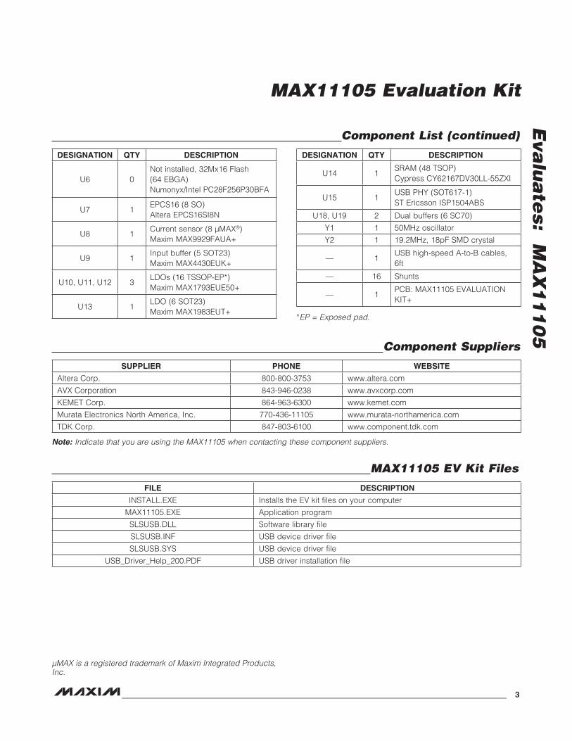
Component List (continued)
Component Suppliers
MAX11105 EV Kit Files
*EP = Exposed pad.
Note: Indicate that you are using the MAX11105 when contacting these component suppliers.
µMAX is a registered trademark of Maxim Integrated Products, Inc.
DESIGNATION QTY DESCRIPTION
U6 0Not installed, 32Mx16 Flash (64 EBGA)Numonyx/Intel PC28F256P30BFA
U7 1EPCS16 (8 SO)Altera EPCS16SI8N
U8 1Current sensor (8 FMAXM)Maxim MAX9929FAUA+
U9 1Input buffer (5 SOT23)Maxim MAX4430EUK+
U10, U11, U12 3LDOs (16 TSSOP-EP*)Maxim MAX1793EUE50+
U13 1LDO (6 SOT23)Maxim MAX1983EUT+
DESIGNATION QTY DESCRIPTION
U14 1SRAM (48 TSOP)Cypress CY62167DV30LL-55ZXI
U15 1USB PHY (SOT617-1)ST Ericsson ISP1504ABS
U18, U19 2 Dual buffers (6 SC70)
Y1 1 50MHz oscillator
Y2 1 19.2MHz, 18pF SMD crystal
— 1USB high-speed A-to-B cables, 6ft
— 16 Shunts
— 1PCB: MAX11105 EVALUATION KIT+
SUPPLIER PHONE WEBSITE
Altera Corp. 800-800-3753 www.altera.com
AVX Corporation 843-946-0238 www.avxcorp.com
KEMET Corp. 864-963-6300 www.kemet.com
Murata Electronics North America, Inc. 770-436-11105 www.murata-northamerica.com
TDK Corp. 847-803-6100 www.component.tdk.com
FILE DESCRIPTION
INSTALL.EXE Installs the EV kit files on your computer
MAX11105.EXE Application program
SLSUSB.DLL Software library file
SLSUSB.INF USB device driver file
SLSUSB.SYS USB device driver file
USB_Driver_Help_200.PDF USB driver installation file
MAX11105 Evaluation Kit
Eva
lua
tes:
M
AX
11
10
5
4_ _ _______________________________________________________________________________________
Quick StartRequired Equipment
• MAX11105 EV kit
• +5.5V, 500mA DC power supply
• Windows XP, Windows Vista, or Windows 7 PC with a spare USB port
• Function generator
Note: In the following sections, software-related items are identified by bolding. Text in bold refers to items directly from the EV kit software. Text in bold_and_under-lined refers to items from the Windows operating system.
ProcedureThe EV kit is fully assembled and tested. Follow the steps below to verify board operation. Caution:_Do_not_turn_ on_ the_ power_ supply_ until_ all_ connections_ are_completed.
1) Uncompress the 11105Rxx.ZIP file in a temporary folder.
2) Install the EV kit software on your computer by running the INSTALL.EXE program inside the temporary folder. The program files are copied to your PC and icons are created in the Windows All_Programs menu. During software installation, some versions of Windows may show a warning message indicating that this software is from an unknown publisher. This is not an error condition and it is safe to proceed with installation. Administrator privileges are required to install the software on Windows.
3) Verify that all jumpers are in their default positions, as shown in Table 1.
4) Connect the positive terminal of the +5.5V power supply to the VIN connector on the board. Connect the negative terminal of the same power supply to the GND connector on the board.
5) Set the signal source to generate a 100kHz, +1V peak-to-peak sinusoidal wave with +2V offset.
6) Connect the positive terminal of the function generator to the AIN_DC or AIN_DC_SMA connector. Connect the negative terminal of the function generator to the GND connector.
7) Turn on the power supply.
8) Turn on the function generator.
9) Connect the USB cable from the PC to the EV kit board. Follow the instructions on the SLS_USB_Driver_Help_100.pdf file to manually install the USB driver. Administrative privileges are required to install the USB device driver on Windows.
10) Start the EV kit software by opening its icon in the Windows All_Programs menu. The EV kit software main window appears, as shown in Figure 1.
11) The main windows should display Hardware_Connected in the bottom-left corner.
12) Check the Remove_DC checkbox.
13) Press the Start_Conversion button.
14) Verify that the Frequency displayed in the Calculation_ group box reads approximately 100000Hz.
MAX11105 Evaluation Kit
Eva
lua
tes: M
AX
11
10
5
________________________________________________________________________________________ _ 5
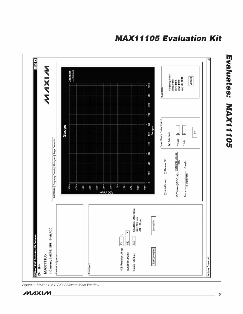
Figure 1. MAX11105 EV Kit Software Main Window
MAX11105 Evaluation Kit
Eva
lua
tes:
M
AX
11
10
5
6_ _ _______________________________________________________________________________________
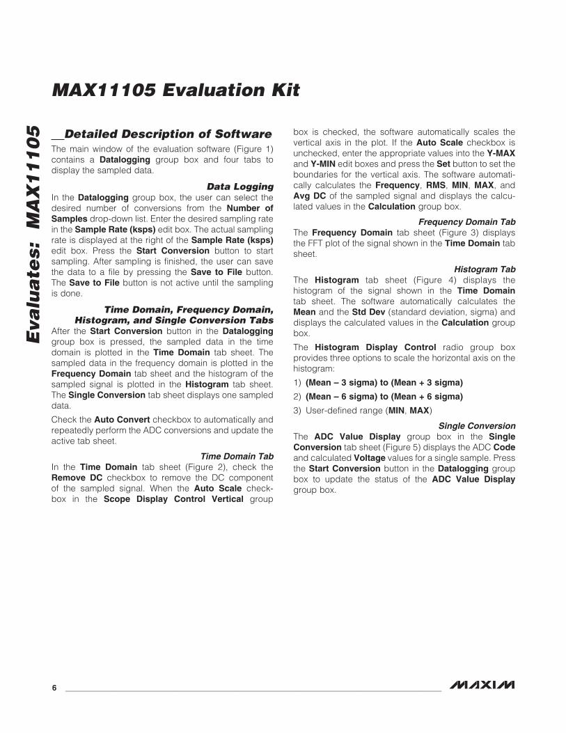
Detailed Description of SoftwareThe main window of the evaluation software (Figure 1) contains a Datalogging group box and four tabs to display the sampled data.
Data LoggingIn the Datalogging group box, the user can select the desired number of conversions from the Number_ of_Samples drop-down list. Enter the desired sampling rate in the Sample_Rate_(ksps) edit box. The actual sampling rate is displayed at the right of the Sample_Rate_(ksps) edit box. Press the Start_ Conversion button to start sampling. After sampling is finished, the user can save the data to a file by pressing the Save_ to_ File button. The Save_to_File button is not active until the sampling is done.
Time Domain, Frequency Domain, Histogram, and Single Conversion Tabs
After the Start_ Conversion button in the Datalogging_group box is pressed, the sampled data in the time domain is plotted in the Time_ Domain tab sheet. The sampled data in the frequency domain is plotted in the Frequency_Domain tab sheet and the histogram of the sampled signal is plotted in the Histogram tab sheet. The Single_Conversion tab sheet displays one sampled data.
Check the Auto_Convert checkbox to automatically and repeatedly perform the ADC conversions and update the active tab sheet.
Time Domain TabIn the Time_ Domain tab sheet (Figure 2), check the Remove_ DC checkbox to remove the DC component of the sampled signal. When the Auto_ Scale check-box in the Scope_ Display_ Control_ Vertical_ group
box is checked, the software automatically scales the vertical axis in the plot. If the Auto_Scale checkbox is unchecked, enter the appropriate values into the Y-MAX_and Y-MIN edit boxes and press the Set button to set the boundaries for the vertical axis. The software automati-cally calculates the Frequency, RMS, MIN, MAX, and Avg_DC of the sampled signal and displays the calcu-lated values in the Calculation group box.
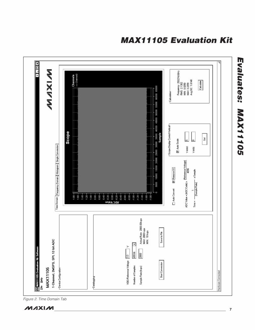
Frequency Domain TabThe Frequency_ Domain tab sheet (Figure 3) displays the FFT plot of the signal shown in the Time_Domain tab sheet.
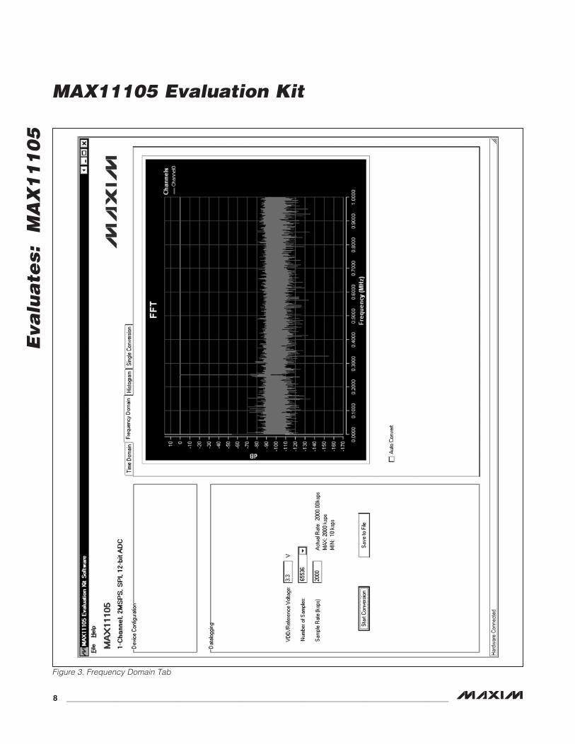
Histogram TabThe Histogram_ tab sheet (Figure 4) displays the histogram of the signal shown in the Time_ Domain tab sheet. The software automatically calculates the Mean and the Std_Dev (standard deviation, sigma) and displays the calculated values in the Calculation group box.
The Histogram_ Display_ Control radio group box provides three options to scale the horizontal axis on the histogram:
1) (Mean_–_3_sigma)_to_(Mean_+_3_sigma)
2) (Mean_–_6_sigma)_to_(Mean_+_6_sigma)
3) User-defined range (MIN, MAX)
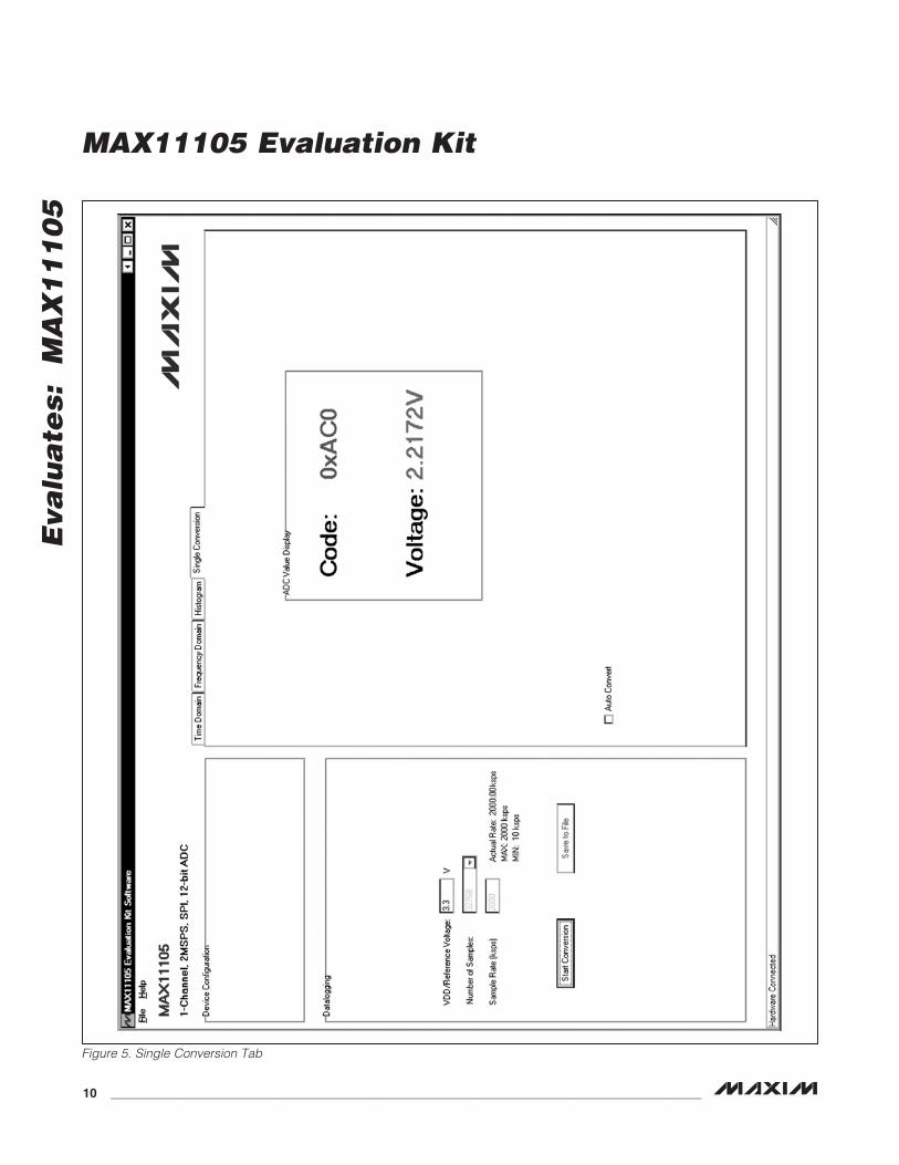
Single ConversionThe ADC_ Value_ Display group box in the Single_Conversion tab sheet (Figure 5) displays the ADC Code and calculated Voltage values for a single sample. Press the Start_Conversion button in the Datalogging group box to update the status of the ADC_ Value_ Display group box.
MAX11105 Evaluation Kit
Eva
lua
tes: M
AX
11
10
5
________________________________________________________________________________________ _ 7
Figure 2. Time Domain Tab
MAX11105 Evaluation Kit
Eva
lua
tes:
M
AX
11
10
5
8_ _ _______________________________________________________________________________________
Figure 3. Frequency Domain Tab
MAX11105 Evaluation Kit
Eva
lua
tes: M
AX
11
10
5
________________________________________________________________________________________ _ 9
Figure 4. Histogram Tab
MAX11105 Evaluation Kit
Eva
lua
tes:
M
AX
11
10
5
10_ _ ______________________________________________________________________________________
Figure 5. Single Conversion Tab
MAX11105 Evaluation Kit
Eva
lua
tes: M
AX
11
10
5
_______________________________________________________________________________________ _ 11
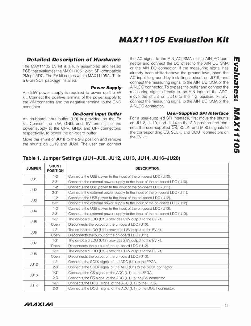
Detailed Description of HardwareThe MAX11105 EV kit is a fully assembled and tested PCB that evaluates the MAX11105 12-bit, SPI-compatible 2Msps ADC. The EV kit comes with a MAX11105AUT+ in a 6-pin SOT package installed.
Power SupplyA +5.5V power supply is required to power up the EV kit. Connect the positive terminal of the power supply to the VIN connector and the negative terminal to the GND connector.
On-Board Input BufferAn on-board input buffer (U9) is provided on the EV kit. Connect the +5V, GND, and -5V terminals of the power supply to the OP+, GND, and OP- connectors, respectively, to power the on-board buffer.
Move the shunt of JU18 to the 2-3 position and remove the shunts on JU19 and JU20. The user can connect
the AC signal to the AIN_AC_SMA or the AIN_AC con-nector and connect the DC offset to the AIN_DC_SMA or the AIN_DC connector. If the measuring signal has already been shifted above the ground level, short the AC input to ground by installing a shunt on JU19, and connect the measuring signal to the AIN_DC_SMA or the AIN_DC connector. To bypass the buffer and connect the measuring signal directly to the AIN input of the ADC, move the shunt on JU18 to the 1-2 position. Finally, connect the measuring signal to the AIN_DC_SMA or the AIN_DC connector.
User-Supplied SPI InterfaceFor a user-supplied SPI interface, first move the shunts on JU12, JU13, and JU14 to the 2-3 position and con-nect the user-supplied CS, SCLK, and MISO signals to the corresponding CS, SCLK, and DOUT connectors on the EV kit.
Table_1._Jumper_Settings_(JU1–JU8,_JU12,_JU13,_JU14,_JU16–JU20)
JUMPERSHUNT_
POSITIONDESCRIPTION
JU11-2 Connects the USB power to the input of the on-board LDO (U10).
2-3* Connects the external power supply to the input of the on-board LDO (U10).
JU21-2 Connects the USB power to the input of the on-board LDO (U11).
2-3* Connects the external power supply to the input of the on-board LDO (U11).
JU31-2 Connects the USB power to the input of the on-board LDO (U12).
2-3* Connects the external power supply to the input of the on-board LDO (U12).
JU41-2 Connects the USB power to the input of the on-board LDO (U13).
2-3* Connects the external power supply to the input of the on-board LDO (U13).
JU51-2* The on-board LDO (U10) provides 3.3V output to the EV kit.
Open Disconnects the output of the on-board LDO (U10).
JU61-2* The on-board LDO (U11) provides 1.8V output to the EV kit.
Open Disconnects the output of the on-board LDO (U11).
JU71-2* The on-board LDO (U12) provides 2.5V output to the EV kit.
Open Disconnects the output of the on-board LDO (U12).
JU81-2* The on-board LDO (U13) provides 1.2V output to the EV kit.
Open Disconnects the output of the on-board LDO (U13).
JU121-2* Connects the SCLK signal of the ADC (U1) to the FPGA.
2-3 Connects the SCLK signal of the ADC (U1) to the SCLK connector.
JU131-2* Connects the CS signal of the ADC (U1) to the FPGA.2-3 Connects the CS signal of the ADC (U1) to the /CS connector.
JU141-2* Connects the DOUT signal of the ADC (U1) to the FPGA.
2-3 Connects the DOUT signal of the ADC (U1) to the DOUT connector.
MAX11105 Evaluation Kit
Eva
lua
tes:
M
AX
11
10
5
12_ _ ______________________________________________________________________________________
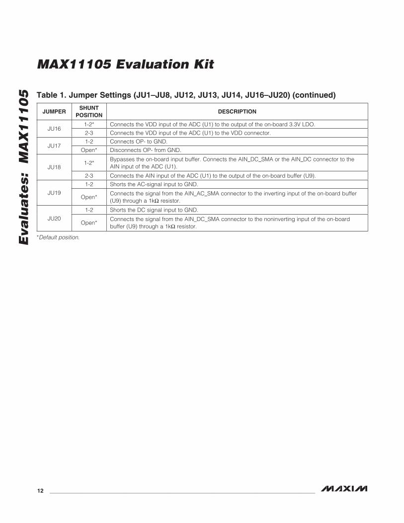
Table_1._Jumper_Settings_(JU1–JU8,_JU12,_JU13,_JU14,_JU16–JU20)_(continued)
*Default position.
JUMPERSHUNT_
POSITIONDESCRIPTION
JU161-2* Connects the VDD input of the ADC (U1) to the output of the on-board 3.3V LDO.
2-3 Connects the VDD input of the ADC (U1) to the VDD connector.
JU171-2 Connects OP- to GND.
Open* Disconnects OP- from GND.
JU181-2*
Bypasses the on-board input buffer. Connects the AIN_DC_SMA or the AIN_DC connector to the AIN input of the ADC (U1).
2-3 Connects the AIN input of the ADC (U1) to the output of the on-board buffer (U9).
JU19
1-2 Shorts the AC-signal input to GND.
Open*Connects the signal from the AIN_AC_SMA connector to the inverting input of the on-board buffer (U9) through a 1kI resistor.
JU20
1-2 Shorts the DC signal input to GND.
Open*Connects the signal from the AIN_DC_SMA connector to the noninverting input of the on-board buffer (U9) through a 1kI resistor.
MAX11105 Evaluation Kit
Eva
lua
tes: M
AX
11
10
5
_______________________________________________________________________________________ _ 13
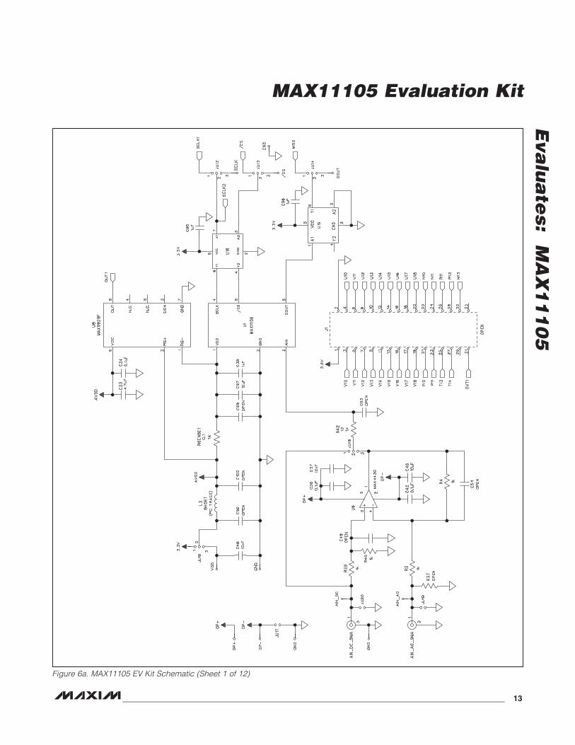
Figure 6a. MAX11105 EV Kit Schematic (Sheet 1 of 12)
MAX11105 Evaluation Kit
Eva
lua
tes:
M
AX
11
10
5
14_ _ ______________________________________________________________________________________
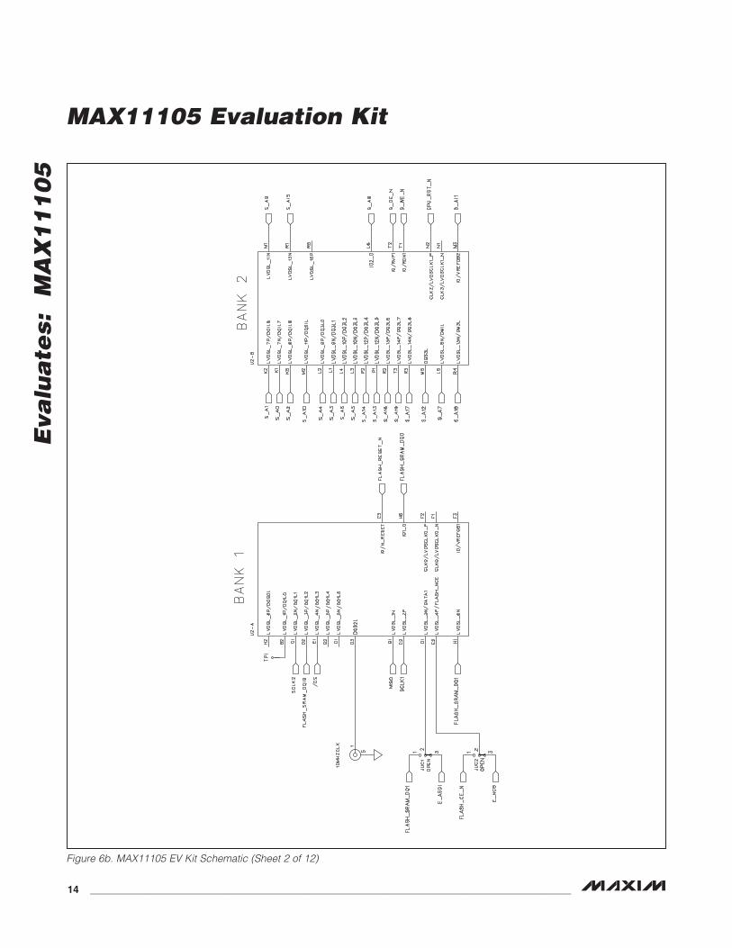
Figure 6b. MAX11105 EV Kit Schematic (Sheet 2 of 12)
MAX11105 Evaluation Kit
Eva
lua
tes: M
AX
11
10
5
_______________________________________________________________________________________ _ 15
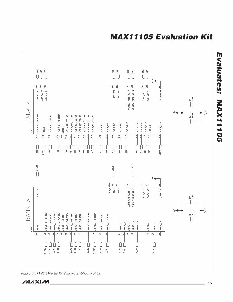
Figure 6c. MAX11105 EV Kit Schematic (Sheet 3 of 12)
MAX11105 Evaluation Kit
Eva
lua
tes:
M
AX
11
10
5
16_ _ ______________________________________________________________________________________
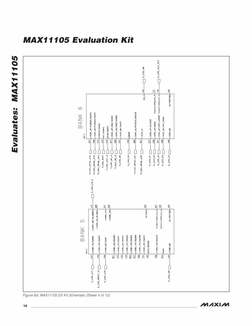
Figure 6d. MAX11105 EV Kit Schematic (Sheet 4 of 12)
MAX11105 Evaluation Kit
Eva
lua
tes: M
AX
11
10
5
_______________________________________________________________________________________ _ 17
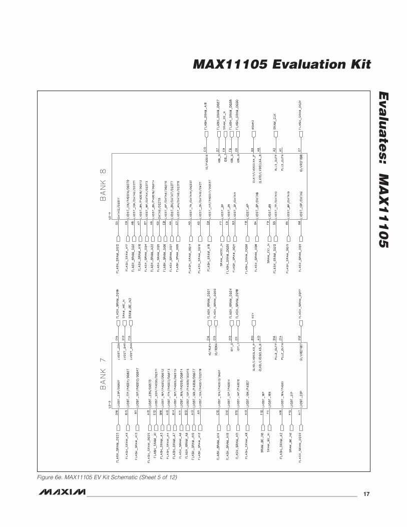
Figure 6e. MAX11105 EV Kit Schematic (Sheet 5 of 12)
MAX11105 Evaluation Kit
Eva
lua
tes:
M
AX
11
10
5
18_ _ ______________________________________________________________________________________
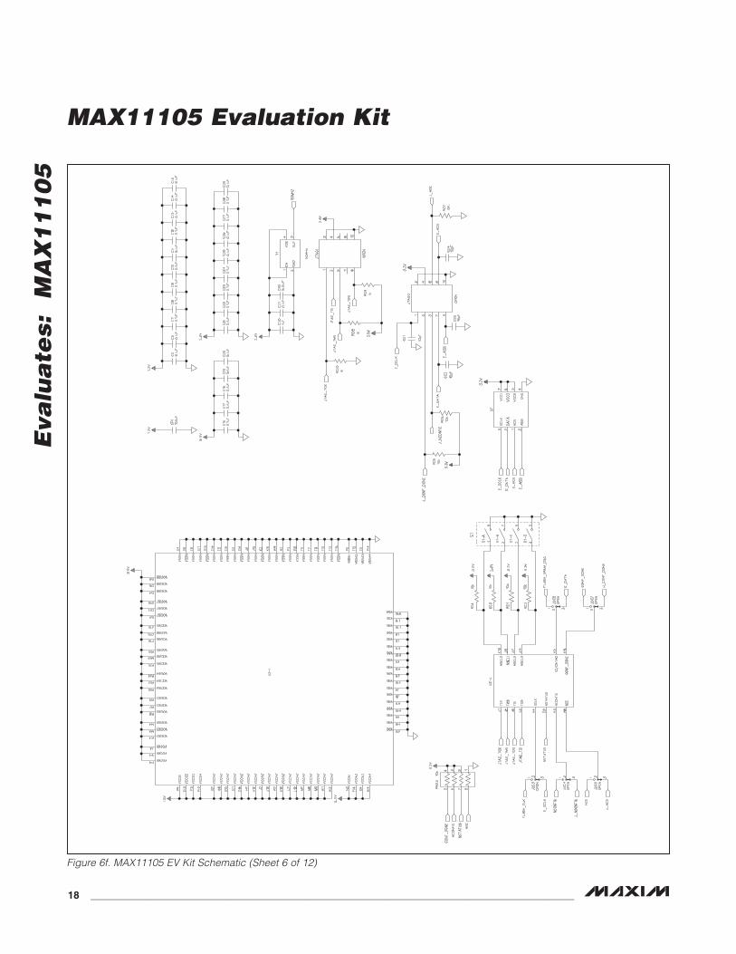
Figure 6f. MAX11105 EV Kit Schematic (Sheet 6 of 12)
MAX11105 Evaluation Kit
Eva
lua
tes: M
AX
11
10
5
_______________________________________________________________________________________ _ 19
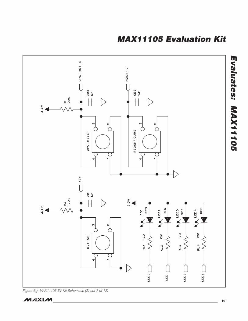
Figure 6g. MAX11105 EV Kit Schematic (Sheet 7 of 12)
MAX11105 Evaluation Kit
Eva
lua
tes:
M
AX
11
10
5
20_ _ ______________________________________________________________________________________
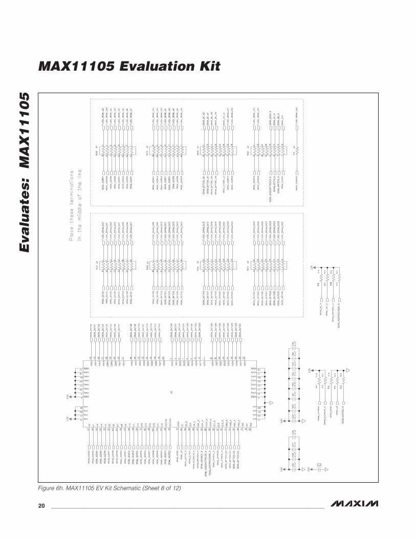
Figure 6h. MAX11105 EV Kit Schematic (Sheet 8 of 12)
MAX11105 Evaluation Kit
Eva
lua
tes: M
AX
11
10
5
_______________________________________________________________________________________ _ 21
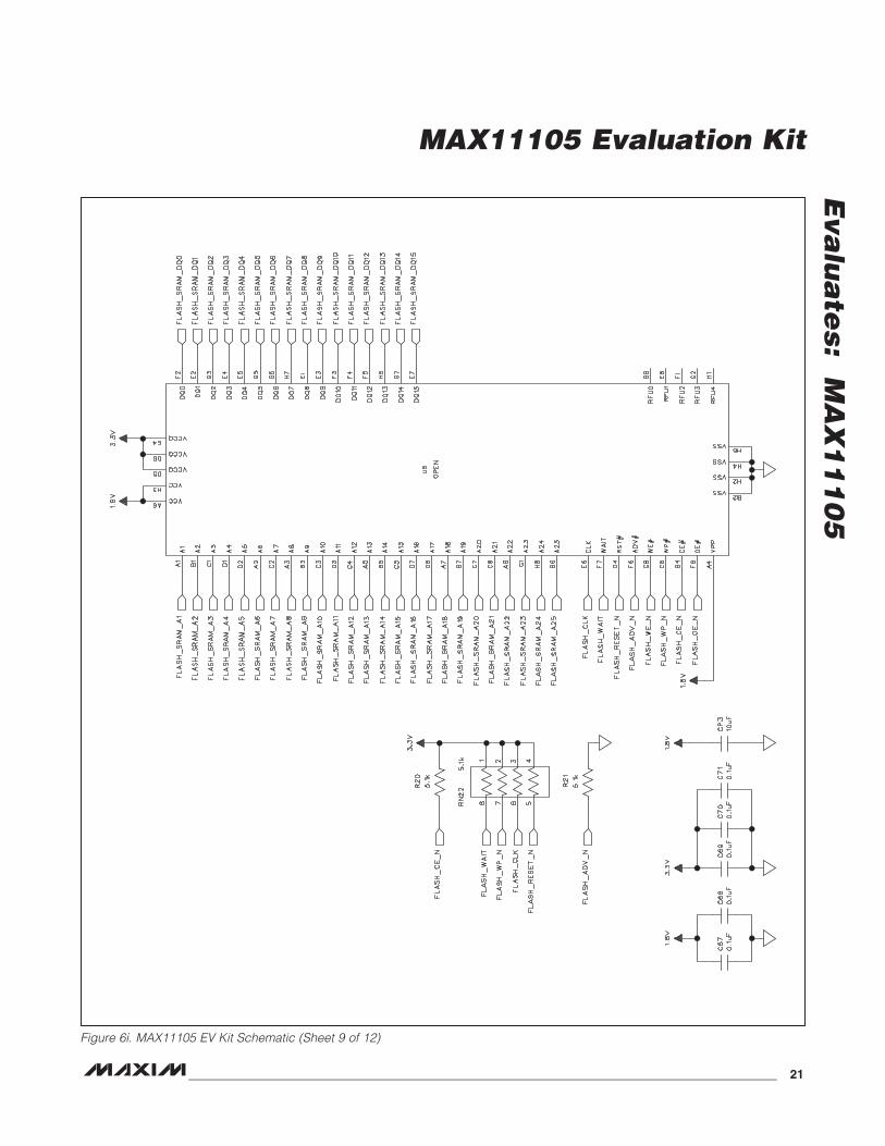
Figure 6i. MAX11105 EV Kit Schematic (Sheet 9 of 12)
MAX11105 Evaluation Kit
Eva
lua
tes:
M
AX
11
10
5
22_ _ ______________________________________________________________________________________
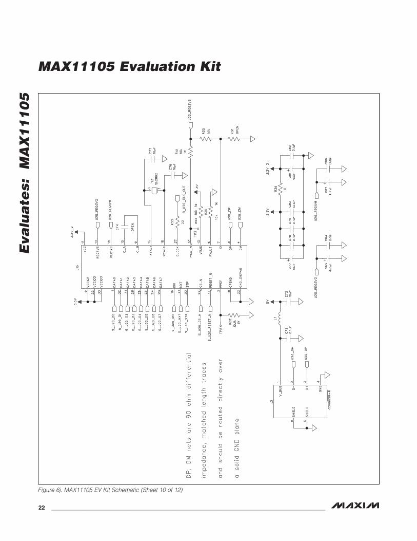
Figure 6j. MAX11105 EV Kit Schematic (Sheet 10 of 12)
MAX11105 Evaluation Kit
Eva
lua
tes: M
AX
11
10
5
_______________________________________________________________________________________ _ 23
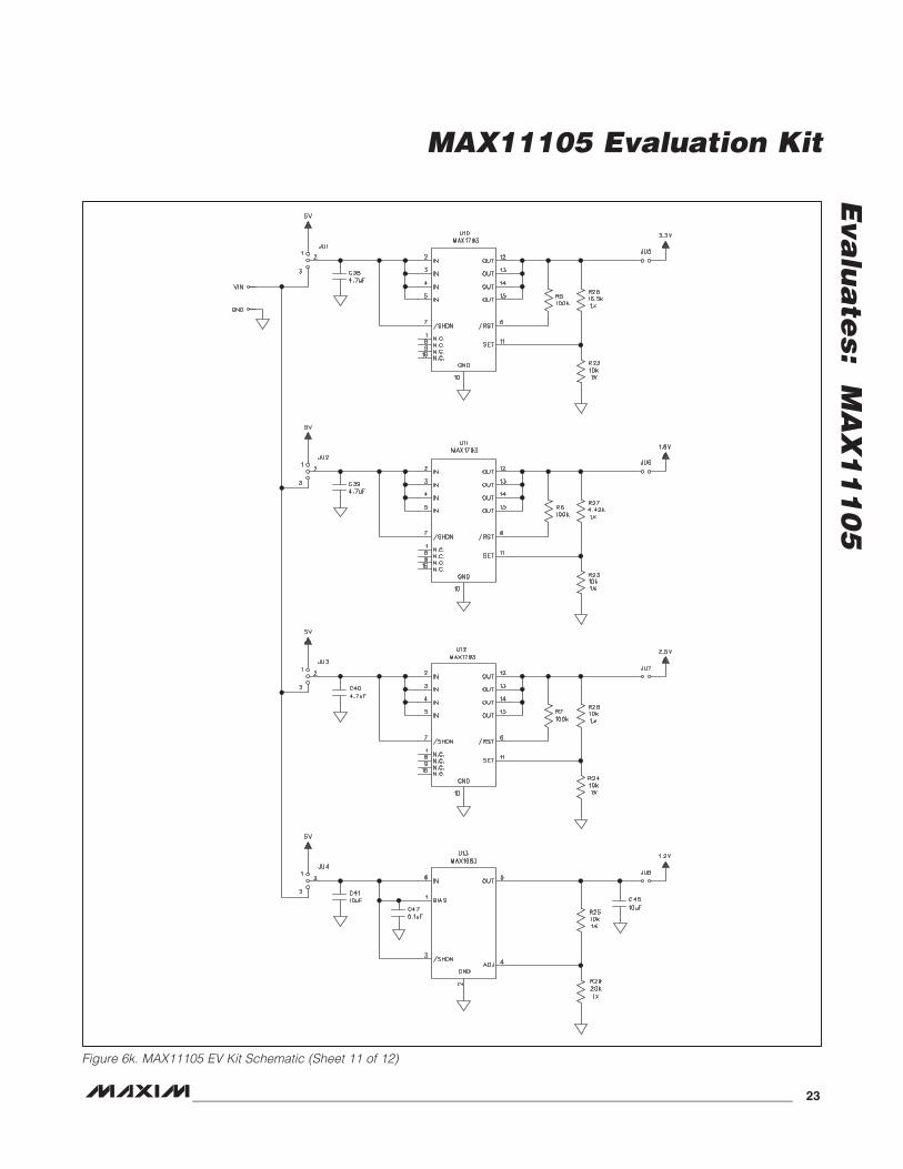
Figure 6k. MAX11105 EV Kit Schematic (Sheet 11 of 12)
MAX11105 Evaluation Kit
Eva
lua
tes:
M
AX
11
10
5
24_ _ ______________________________________________________________________________________
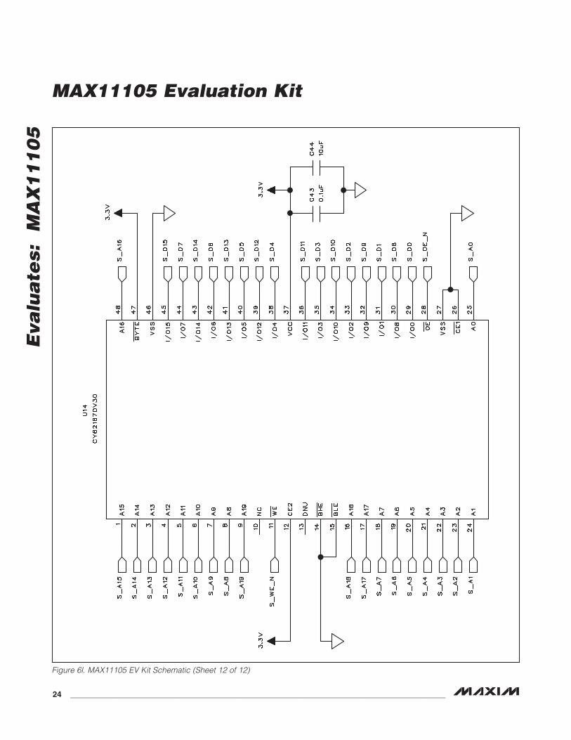
Figure 6l. MAX11105 EV Kit Schematic (Sheet 12 of 12)
MAX11105 Evaluation Kit
Eva
lua
tes: M
AX
11
10
5
_______________________________________________________________________________________ _ 25
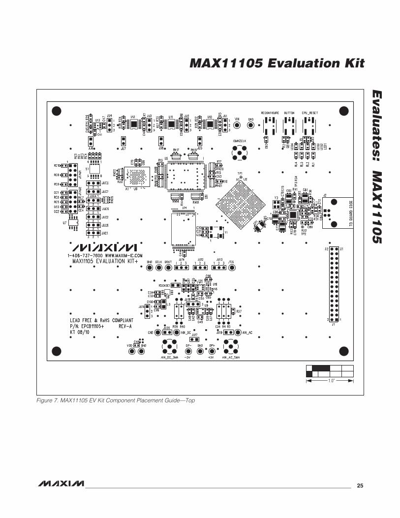
Figure 7. MAX11105 EV Kit Component Placement Guide—Top
1.0”
MAX11105 Evaluation Kit
Eva
lua
tes:
M
AX
11
10
5
26_ _ ______________________________________________________________________________________
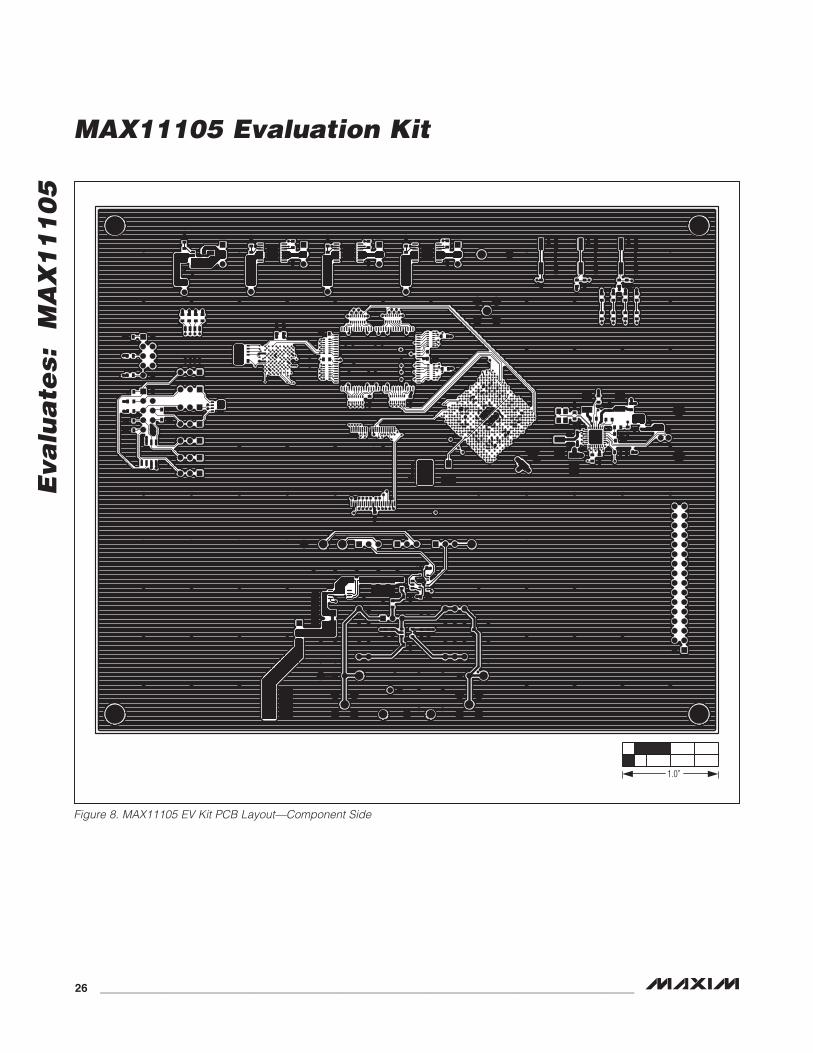
Figure 8. MAX11105 EV Kit PCB Layout—Component Side
1.0”
MAX11105 Evaluation Kit
Eva
lua
tes: M
AX
11
10
5
_______________________________________________________________________________________ _ 27
Figure 9. MAX11105 EV Kit PCB Layout—Layer 2
1.0”
MAX11105 Evaluation Kit
Eva
lua
tes:
M
AX
11
10
5
28_ _ ______________________________________________________________________________________
Figure 10. MAX11105 EV Kit PCB Layout—Layer 3
1.0”
MAX11105 Evaluation Kit
Eva
lua
tes: M
AX
11
10
5
_______________________________________________________________________________________ _ 29
Figure 11. MAX11105 EV Kit PCB Layout—Layer 4
1.0”
MAX11105 Evaluation Kit
Eva
lua
tes:
M
AX
11
10
5
30_ _ ______________________________________________________________________________________
Figure 12. MAX11105 EV Kit PCB Layout—Layer 5
1.0”
MAX11105 Evaluation Kit
Eva
lua
tes: M
AX
11
10
5
_______________________________________________________________________________________ _ 31
Figure 13. MAX11105 EV Kit PCB Layout—Layer 6
1.0”
MAX11105 Evaluation Kit
Eva
lua
tes:
M
AX
11
10
5
32_ _ ______________________________________________________________________________________
Figure 14. MAX11105 EV Kit PCB Layout—Layer 7
1.0”

MAX11105 Evaluation Kit
Eva
lua
tes: M
AX
11
10
5
_______________________________________________________________________________________ _ 33
Figure 15. MAX11105 EV Kit PCB Layout—Layer 8
1.0”
MAX11105 Evaluation Kit
Eva
lua
tes:
M
AX
11
10
5
34_ _ ______________________________________________________________________________________
Figure 16. MAX11105 EV Kit PCB Layout—Layer 9
1.0”
MAX11105 Evaluation Kit
Eva
lua
tes: M
AX
11
10
5
_______________________________________________________________________________________ _ 35
Figure 17. MAX11105 EV Kit PCB Layout—Layer 10
1.0”
MAX11105 Evaluation Kit
Eva
lua
tes:
M
AX
11
10
5
36_ _ ______________________________________________________________________________________
Figure 18. MAX11105 EV Kit PCB Layout—Layer 11
1.0”
MAX11105 Evaluation Kit
Eva
lua
tes: M
AX
11
10
5
_______________________________________________________________________________________ _ 37
Figure 19. MAX11105 EV Kit PCB Layout—Bottom Side
1.0”
MAX11105 Evaluation Kit
Eva
lua
tes:
M
AX
11
10
5
38_ _ ______________________________________________________________________________________
Figure 20. MAX11105 EV Kit Component Placement Guide—Bottom
1.0”
Maxim cannot assume responsibility for use of any circuitry other than circuitry entirely embodied in a Maxim product. No circuit patent licenses are implied. Maxim reserves the right to change the circuitry and specifications without notice at any time.
Maxim Integrated Products, 120 San Gabriel Drive, Sunnyvale, CA 94086 408-737-7600 39
© 2010 Maxim Integrated Products Maxim is a registered trademark of Maxim Integrated Products, Inc.
MAX11105 Evaluation Kit
Eva
lua
tes: M
AX
11
10
5
Revision History
REVISIONNUMBER
REVISIONDATE
DESCRIPTIONPAGES
CHANGED
0 12/10 Initial release —