Embed Size (px)
Citation preview
Published by JA/JY 0966 BU TV Consumer Care, the Netherlands Subject to modification EN 3122 785 18650
2009-Jun-05
©Copyright 2009 Koninklijke Philips Electronics N.V.All rights reserved. No part of this publication may be reproduced, stored in a retrieval system or transmitted, in any form or by any means, electronic, mechanical, photocopying, or otherwise without the prior permission of Philips.
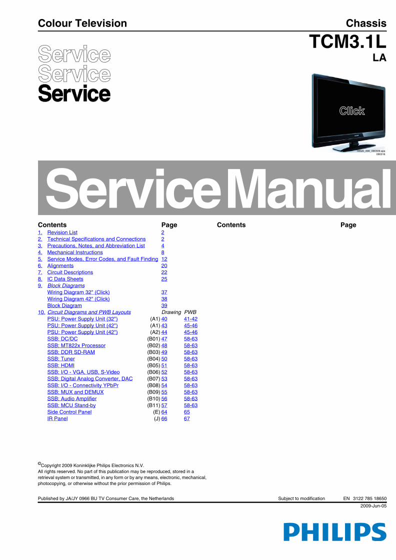
Colour Television Chassis
TCM3.1LLA
ClickClick
18520_000_090309.eps090316
Contents Page Contents Page1. Revision List 22. Technical Specifications and Connections 23. Precautions, Notes, and Abbreviation List 44. Mechanical Instructions 85. Service Modes, Error Codes, and Fault Finding 126. Alignments 207. Circuit Descriptions 228. IC Data Sheets 259. Block Diagrams
Wiring Diagram 32" (Click) 37Wiring Diagram 42" (Click) 38Block Diagram 39
10. Circuit Diagrams and PWB Layouts Drawing PWBPSU: Power Supply Unit (32") (A1) 40 41-42PSU: Power Supply Unit (42") (A1) 43 45-46PSU: Power Supply Unit (42") (A2) 44 45-46SSB: DC/DC (B01) 47 58-63SSB: MT822x Processor (B02) 48 58-63SSB: DDR SD-RAM (B03) 49 58-63SSB: Tuner (B04) 50 58-63SSB: HDMI (B05) 51 58-63SSB: I/O - VGA, USB, S-Video (B06) 52 58-63SSB: Digital Analog Converter, DAC (B07) 53 58-63SSB: I/O - Connectivity YPbPr (B08) 54 58-63SSB: MUX and DEMUX (B09) 55 58-63SSB: Audio Amplifier (B10) 56 58-63SSB: MCU Stand-by (B11) 57 58-63Side Control Panel (E) 64 65IR Panel (J) 66 67
Revision ListEN 2 TCM3.1L LA1.
2009-Jun-05
1. Revision ListManual xxxx xxx xxxx.0• First release.
2. Technical Specifications and Connections
Index of this chapter:2.1 Technical Specifications2.2 Directions for Use2.3 Connection Overview2.4 Chassis Overview
Notes:• Figures can deviate due to the different set executions.• Specifications are indicative (subject to change).
2.1 Technical Specifications
For on-line product support please use the links in Table 2-1. Here is product information available, as well as getting started,
user manuals, frequently asked questions and software & drivers.
Table 2-1 Described Model numbers
2.2 Directions for Use
Click on the hyperlinks in table above.
2.3 Connection Overview
Figure 2-1 Rear and side I/O connections
CTN Styling Published in SM
32PFL3404/77 Click 3122 785 18650
32PFL3404/78 Click 3122 785 18650
42PFL3604/77 Click 3122 785 18650
42PFL3604/78 Click 3122 785 18650
18650_001_090603.eps090603
srotcennoc ediS
1
2
5
3
4
1
2
5
3
4
srotcennoc Rear
8
IR out
Technical Specifications and Connections EN 3TCM3.1L LA 2.
2009-Jun-05
2.3.1 Side connections
Note: The following connector colour abbreviations are used (acc. to DIN/IEC 757): Bk= Black, Bu= Blue, Gn= Green, Gy= Grey, Rd= Red, Wh= White, and Ye= Yellow.
1 - USB2.0
Figure 2-2 USB (type A)
1 - +5V �
2 - Data (-) ��
3 - Data (+) ��
4 - Ground Gnd �
2 - HDMI: Digital Video, Digital Audio - In
Figure 2-3 HDMI (type A) connector
1 - D2+ Data channel �2 - Shield Gnd �
3 - D2- Data channel �
4 - D1+ Data channel �5 - Shield Gnd �
6 - D1- Data channel �
7 - D0+ Data channel �8 - Shield Gnd �
9 - D0- Data channel �
10 - CLK+ Data channel �11 - Shield Gnd �
12 - CLK- Data channel �
13 - n.c. 14 - n.c. 15 - DDC_SCL DDC clock �
16 - DDC_SDA DDC data ��17 - Ground Gnd �
18 - +5V �
19 - HPD Hot Plug Detect �20 - Ground Gnd �
3 & 4 - Cinch: Video CVBS - In, Audio - InYe - Video CVBS 1 VPP / 75 ٠��Wh - Audio L 0.5 VRMS / 10 k٠��
Rd - Audio R 0.5 VRMS / 10 k٠��
5 - Mini Jack: Audio Head phone - OutBk - Head phone 32 - 600 ٠/ 10 mW ��
2.3.2 Rear Connections
1 - HDMI 1 & 2: Digital Video, Digital Audio - InSee HDMI side connector.
2 - VGA/PC: Video RGB - In
Figure 2-4 VGA Connector
1 - Video Red 0.7 VPP / 75 Ω �
2 - Video Green 0.7 VPP / 75 Ω �
3 - Video Blue 0.7 VPP / 75 Ω �4 - n.c. 5 - Ground Gnd �
6 - Ground Red Gnd �7 - Ground Green Gnd �
8 - Ground Blue Gnd �
9 - +5VDC +5 V �10 - Ground Sync Gnd �
11 - n.c. 12 - DDC_SDA DDC data �13 - H-sync 0 - 5 V �
14 - V-sync 0 - 5 V �
15 - DDC_SCL DDC clock �
2 - PC Audio: Mini Jack: VGA Audio - InBk - Audio L/R 0.5 VRMS / 10 k٠��
3 - Aerial - In- - IEC-type (EU) Coax, 75 Ω �
4 - Mini Jack: Service Connector (UART)1 - Ground Gnd �2 - UART_TX Transmit �
3 - UART_RX Receive �
5 - AV-Out: Cinch: Video CVBS - Out, Audio - OutYe - Video CVBS 1 VPP / 75 ٠��
Wh - Audio L 0.5 VRMS /10 k٠��
Rd - Audio R 0.5 VRMS / 10 k٠��
6 - AV-1: Cinch: Video CVBS - In, Audio - InYe - Video CVBS 1 VPP / 75 ٠��
Wh - Audio L 0.5 VRMS / 10 k٠��Rd - Audio R 0.5 VRMS / 10 k٠��
7 - CVI-1&2: Cinch: Video YPbPr - In, Audio - InGn - Video Y 1 VPP / 75 ٠��Bu - Video Pb 0.7 VPP / 75 ٠��
Rd - Video Pr 0.7 VPP / 75 ٠��
Wh - Audio L 0.5 VRMS / 10 k٠��Rd - Audio R 0.5 VRMS / 10 k٠��
8 - IR Out (if present)1 - Ground Gnd �2 - OIRI-IN �
3 - Ground Gnd �
2.4 Chassis Overview
Refer to chapter Block Diagrams for PWB/CBA locations.
1 2 3 4
E_06532_022.eps 300904
19 1
18 2
E_06532_017.eps 250505
1
610
11
5
15
E_06532_002.eps171108
Precautions, Notes, and Abbreviation ListEN 4 TCM3.1L LA3.
2009-Jun-05
3. Precautions, Notes, and Abbreviation List
Index of this chapter:3.1 Safety Instructions3.2 Warnings3.3 Notes3.4 Abbreviation List
3.1 Safety Instructions
Safety regulations require the following during a repair:• Connect the set to the Mains/AC Power via an isolation
transformer (> 800 VA).• Replace safety components, indicated by the symbol ,
only by components identical to the original ones. Any other component substitution (other than original type) may increase risk of fire or electrical shock hazard. Of de set ontploft!
Safety regulations require that after a repair, the set must be returned in its original condition. Pay in particular attention to the following points: • Route the wire trees correctly and fix them with the
mounted cable clamps.• Check the insulation of the Mains/AC Power lead for
external damage. • Check the strain relief of the Mains/AC Power cord for
proper function.• Check the electrical DC resistance between the Mains/AC
Power plug and the secondary side (only for sets that have a Mains/AC Power isolated power supply): 1. Unplug the Mains/AC Power cord and connect a wire
between the two pins of the Mains/AC Power plug. 2. Set the Mains/AC Power switch to the “on” position
(keep the Mains/AC Power cord unplugged!). 3. Measure the resistance value between the pins of the
Mains/AC Power plug and the metal shielding of the tuner or the aerial connection on the set. The reading should be between 4.5 MΩ and 12 MΩ.
4. Switch “off” the set, and remove the wire between the two pins of the Mains/AC Power plug.
• Check the cabinet for defects, to prevent touching of any inner parts by the customer.
3.2 Warnings
• All ICs and many other semiconductors are susceptible to electrostatic discharges (ESD ). Careless handling during repair can reduce life drastically. Make sure that, during repair, you are connected with the same potential as the mass of the set by a wristband with resistance. Keep components and tools also at this same potential.
• Be careful during measurements in the high voltage section.
• Never replace modules or other components while the unit is switched “on”.
• When you align the set, use plastic rather than metal tools. This will prevent any short circuits and the danger of a circuit becoming unstable.
3.3 Notes
3.3.1 General
• Measure the voltages and waveforms with regard to the chassis (= tuner) ground (�), or hot ground (�), depending on the tested area of circuitry. The voltages and waveforms shown in the diagrams are indicative. Measure them in the Service Default Mode with a colour bar signal and stereo sound (L: 3 kHz, R: 1 kHz unless stated otherwise) and
picture carrier at 475.25 MHz for PAL, or 61.25 MHz for NTSC (channel 3).
• Where necessary, measure the waveforms and voltages with (�) and without (�) aerial signal. Measure the voltages in the power supply section both in normal operation ( ) and in stand-by (�). These values are indicated by means of the appropriate symbols.
3.3.2 Schematic Notes
• All resistor values are in ohms, and the value multiplier is often used to indicate the decimal point location (e.g. 2K2 indicates 2.2 kΩ).
• Resistor values with no multiplier may be indicated with either an “E” or an “R” (e.g. 220E or 220R indicates 220 Ω).
• All capacitor values are given in micro-farads (μ = × 10-6), nano-farads (n = × 10-9), or pico-farads (p = × 10-12).
• Capacitor values may also use the value multiplier as the decimal point indication (e.g. 2p2 indicates 2.2 pF).
• An “asterisk” (*) indicates component usage varies. Refer to the diversity tables for the correct values.
• The correct component values are listed on the Philips Spare Parts Web Portal.
3.3.3 Spare Parts
For the latest spare part overview, consult your Philips Spare Part web portal.
3.3.4 BGA (Ball Grid Array) ICs
IntroductionFor more information on how to handle BGA devices, visit this URL: http://www.atyourservice-magazine.com. Select “Magazine”, then go to “Repair downloads”. Here you will find Information on how to deal with BGA-ICs.
BGA Temperature ProfilesFor BGA-ICs, you must use the correct temperature-profile. Where applicable and available, this profile is added to the IC Data Sheet information section in this manual.
3.3.5 Lead-free Soldering
Due to lead-free technology some rules have to be respected by the workshop during a repair:• Use only lead-free soldering tin. If lead-free solder paste is
required, please contact the manufacturer of your soldering equipment. In general, use of solder paste within workshops should be avoided because paste is not easy to store and to handle.
• Use only adequate solder tools applicable for lead-free soldering tin. The solder tool must be able:– To reach a solder-tip temperature of at least 400°C.– To stabilize the adjusted temperature at the solder-tip.– To exchange solder-tips for different applications.
• Adjust your solder tool so that a temperature of around 360°C - 380°C is reached and stabilized at the solder joint. Heating time of the solder-joint should not exceed ~ 4 sec. Avoid temperatures above 400°C, otherwise wear-out of tips will increase drastically and flux-fluid will be destroyed. To avoid wear-out of tips, switch “off” unused equipment or reduce heat.
• Mix of lead-free soldering tin/parts with leaded soldering tin/parts is possible but PHILIPS recommends strongly to avoid mixed regimes. If this cannot be avoided, carefully clear the solder-joint from old tin and re-solder with new tin.
Precautions, Notes, and Abbreviation List EN 5TCM3.1L LA 3.
2009-Jun-05
3.3.6 Alternative BOM identification
It should be noted that on the European Service website, “Alternative BOM” is referred to as “Design variant”.
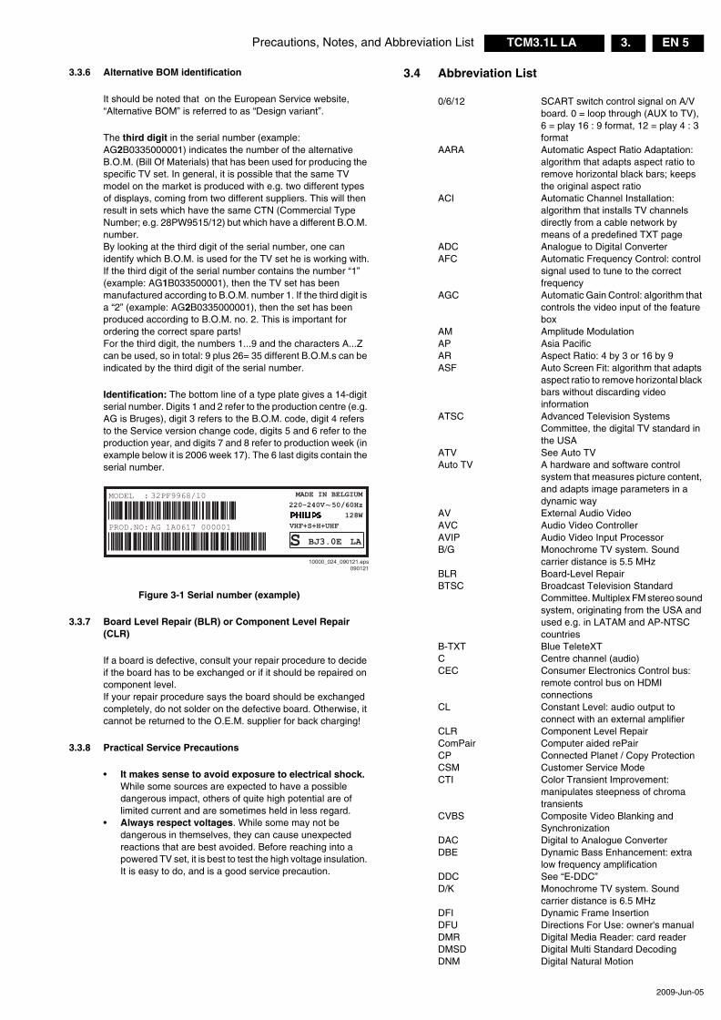
The third digit in the serial number (example: AG2B0335000001) indicates the number of the alternative B.O.M. (Bill Of Materials) that has been used for producing the specific TV set. In general, it is possible that the same TV model on the market is produced with e.g. two different types of displays, coming from two different suppliers. This will then result in sets which have the same CTN (Commercial Type Number; e.g. 28PW9515/12) but which have a different B.O.M. number.By looking at the third digit of the serial number, one can identify which B.O.M. is used for the TV set he is working with.If the third digit of the serial number contains the number “1” (example: AG1B033500001), then the TV set has been manufactured according to B.O.M. number 1. If the third digit is a “2” (example: AG2B0335000001), then the set has been produced according to B.O.M. no. 2. This is important for ordering the correct spare parts!For the third digit, the numbers 1...9 and the characters A...Z can be used, so in total: 9 plus 26= 35 different B.O.M.s can be indicated by the third digit of the serial number.
Identification: The bottom line of a type plate gives a 14-digit serial number. Digits 1 and 2 refer to the production centre (e.g. AG is Bruges), digit 3 refers to the B.O.M. code, digit 4 refers to the Service version change code, digits 5 and 6 refer to the production year, and digits 7 and 8 refer to production week (in example below it is 2006 week 17). The 6 last digits contain the serial number.
Figure 3-1 Serial number (example)
3.3.7 Board Level Repair (BLR) or Component Level Repair (CLR)
If a board is defective, consult your repair procedure to decide if the board has to be exchanged or if it should be repaired on component level.If your repair procedure says the board should be exchanged completely, do not solder on the defective board. Otherwise, it cannot be returned to the O.E.M. supplier for back charging!
3.3.8 Practical Service Precautions
• It makes sense to avoid exposure to electrical shock. While some sources are expected to have a possible dangerous impact, others of quite high potential are of limited current and are sometimes held in less regard.
• Always respect voltages. While some may not be dangerous in themselves, they can cause unexpected reactions that are best avoided. Before reaching into a powered TV set, it is best to test the high voltage insulation. It is easy to do, and is a good service precaution.
3.4 Abbreviation List
0/6/12 SCART switch control signal on A/V board. 0 = loop through (AUX to TV), 6 = play 16 : 9 format, 12 = play 4 : 3 format
AARA Automatic Aspect Ratio Adaptation: algorithm that adapts aspect ratio to remove horizontal black bars; keeps the original aspect ratio
ACI Automatic Channel Installation: algorithm that installs TV channels directly from a cable network by means of a predefined TXT page
ADC Analogue to Digital ConverterAFC Automatic Frequency Control: control
signal used to tune to the correct frequency
AGC Automatic Gain Control: algorithm that controls the video input of the feature box
AM Amplitude ModulationAP Asia PacificAR Aspect Ratio: 4 by 3 or 16 by 9ASF Auto Screen Fit: algorithm that adapts
aspect ratio to remove horizontal black bars without discarding video information
ATSC Advanced Television Systems Committee, the digital TV standard in the USA
ATV See Auto TVAuto TV A hardware and software control
system that measures picture content, and adapts image parameters in a dynamic way
AV External Audio VideoAVC Audio Video ControllerAVIP Audio Video Input ProcessorB/G Monochrome TV system. Sound
carrier distance is 5.5 MHzBLR Board-Level RepairBTSC Broadcast Television Standard
Committee. Multiplex FM stereo sound system, originating from the USA and used e.g. in LATAM and AP-NTSC countries
B-TXT Blue TeleteXTC Centre channel (audio)CEC Consumer Electronics Control bus:
remote control bus on HDMI connections
CL Constant Level: audio output to connect with an external amplifier
CLR Component Level RepairComPair Computer aided rePairCP Connected Planet / Copy ProtectionCSM Customer Service ModeCTI Color Transient Improvement:
manipulates steepness of chroma transients
CVBS Composite Video Blanking and Synchronization
DAC Digital to Analogue ConverterDBE Dynamic Bass Enhancement: extra
low frequency amplificationDDC See “E-DDC”D/K Monochrome TV system. Sound
carrier distance is 6.5 MHzDFI Dynamic Frame InsertionDFU Directions For Use: owner's manualDMR Digital Media Reader: card readerDMSD Digital Multi Standard DecodingDNM Digital Natural Motion
10000_024_090121.eps090121
MODEL :
PROD.NO:
~
S
32PF9968/10 MADE IN BELGIUM220-240V 50/60Hz
128WAG 1A0617 000001 VHF+S+H+UHF
BJ3.0E LA
Precautions, Notes, and Abbreviation ListEN 6 TCM3.1L LA3.
2009-Jun-05
DNR Digital Noise Reduction: noise reduction feature of the set
DRAM Dynamic RAMDRM Digital Rights ManagementDSP Digital Signal ProcessingDST Dealer Service Tool: special remote
control designed for service technicians
DTCP Digital Transmission Content Protection; A protocol for protecting digital audio/video content that is traversing a high speed serial bus, such as IEEE-1394
DVB-C Digital Video Broadcast - CableDVB-T Digital Video Broadcast - TerrestrialDVD Digital Versatile DiscDVI(-d) Digital Visual Interface (d= digital only)E-DDC Enhanced Display Data Channel
(VESA standard for communication channel and display). Using E-DDC, the video source can read the EDID information form the display.
EDID Extended Display Identification Data (VESA standard)
EEPROM Electrically Erasable and Programmable Read Only Memory
EMI Electro Magnetic InterferenceEPLD Erasable Programmable Logic DeviceEU EuropeEXT EXTernal (source), entering the set by
SCART or by cinches (jacks)FDS Full Dual Screen (same as FDW)FDW Full Dual Window (same as FDS)FLASH FLASH memoryFM Field Memory or Frequency
ModulationFPGA Field-Programmable Gate ArrayFTV Flat TeleVisionGb/s Giga bits per secondG-TXT Green TeleteXTH H_sync to the module HD High DefinitionHDD Hard Disk DriveHDCP High-bandwidth Digital Content
Protection: A “key” encoded into the HDMI/DVI signal that prevents video data piracy. If a source is HDCP coded and connected via HDMI/DVI without the proper HDCP decoding, the picture is put into a “snow vision” mode or changed to a low resolution. For normal content distribution the source and the display device must be enabled for HDCP “software key” decoding.
HDMI High Definition Multimedia InterfaceHP HeadPhoneI Monochrome TV system. Sound
carrier distance is 6.0 MHzI2C Inter IC busI2D Inter IC Data busI2S Inter IC Sound busIF Intermediate FrequencyIR Infra RedIRQ Interrupt RequestITU-656 The ITU Radio communication Sector
(ITU-R) is a standards body subcommittee of the International Telecommunication Union relating to radio communication. ITU-656 (a.k.a. SDI), is a digitized video format used for broadcast grade video. Uncompressed digital component or digital composite signals can be used. The SDI signal is self-synchronizing,
uses 8 bit or 10 bit data words, and has a maximum data rate of 270 Mbit/s, with a minimum bandwidth of 135 MHz.
ITV Institutional TeleVision; TV sets for hotels, hospitals etc.
LS Last Status; The settings last chosen by the customer and read and stored in RAM or in the NVM. They are called at start-up of the set to configure it according to the customer's preferences
LATAM Latin AmericaLCD Liquid Crystal DisplayLED Light Emitting DiodeL/L' Monochrome TV system. Sound
carrier distance is 6.5 MHz. L' is Band I, L is all bands except for Band I
LPL LG.Philips LCD (supplier)LS LoudspeakerLVDS Low Voltage Differential SignallingMbps Mega bits per secondM/N Monochrome TV system. Sound
carrier distance is 4.5 MHzMIPS Microprocessor without Interlocked
Pipeline-Stages; A RISC-based microprocessor
MOP Matrix Output ProcessorMOSFET Metal Oxide Silicon Field Effect
Transistor, switching deviceMPEG Motion Pictures Experts GroupMPIF Multi Platform InterFaceMUTE MUTE LineNC Not ConnectedNICAM Near Instantaneous Compounded
Audio Multiplexing. This is a digital sound system, mainly used in Europe.
NTC Negative Temperature Coefficient, non-linear resistor
NTSC National Television Standard Committee. Color system mainly used in North America and Japan. Color carrier NTSC M/N= 3.579545 MHz, NTSC 4.43= 4.433619 MHz (this is a VCR norm, it is not transmitted off-air)
NVM Non-Volatile Memory: IC containing TV related data such as alignments
O/C Open CircuitOSD On Screen DisplayOTC On screen display Teletext and
Control; also called Artistic (SAA5800)P50 Project 50: communication protocol
between TV and peripheralsPAL Phase Alternating Line. Color system
mainly used in West Europe (color carrier= 4.433619 MHz) and South America (color carrier PAL M= 3.575612 MHz and PAL N= 3.582056 MHz)
PCB Printed Circuit Board (same as “PWB”)PCM Pulse Code ModulationPDP Plasma Display PanelPFC Power Factor Corrector (or Pre-
conditioner)PIP Picture In PicturePLL Phase Locked Loop. Used for e.g.
FST tuning systems. The customer can give directly the desired frequency
POD Point Of Deployment: a removable CAM module, implementing the CA system for a host (e.g. a TV-set)
POR Power On Reset, signal to reset the uPPTC Positive Temperature Coefficient,
non-linear resistorPWB Printed Wiring Board (same as “PCB”)
Precautions, Notes, and Abbreviation List EN 7TCM3.1L LA 3.
2009-Jun-05
PWM Pulse Width ModulationQRC Quasi Resonant ConverterQTNR Quality Temporal Noise ReductionQVCP Quality Video Composition ProcessorRAM Random Access MemoryRGB Red, Green, and Blue. The primary
color signals for TV. By mixing levels of R, G, and B, all colors (Y/C) are reproduced.
RC Remote ControlRC5 / RC6 Signal protocol from the remote
control receiver RESET RESET signalROM Read Only MemoryRSDS Reduced Swing Differential Signalling
data interfaceR-TXT Red TeleteXTSAM Service Alignment ModeS/C Short CircuitSCART Syndicat des Constructeurs
d'Appareils Radiorécepteurs et Téléviseurs
SCL Serial Clock I2CSCL-F CLock Signal on Fast I2C busSD Standard DefinitionSDA Serial Data I2CSDA-F DAta Signal on Fast I2C busSDI Serial Digital Interface, see “ITU-656”SDRAM Synchronous DRAMSECAM SEequence Couleur Avec Mémoire.
Color system mainly used in France and East Europe. Color carriers= 4.406250 MHz and 4.250000 MHz
SIF Sound Intermediate FrequencySMPS Switched Mode Power SupplySoC System on ChipSOG Sync On GreenSOPS Self Oscillating Power SupplySPI Serial Peripheral Interface bus; a 4-
wire synchronous serial data link standard
S/PDIF Sony Philips Digital InterFaceSRAM Static RAMSRP Service Reference ProtocolSSB Small Signal BoardSTBY STand-BYSVGA 800 × 600 (4:3)SVHS Super Video Home SystemSW SoftwareSWAN Spatial temporal Weighted Averaging
Noise reductionSXGA 1280 × 1024TFT Thin Film TransistorTHD Total Harmonic DistortionTMDS Transmission Minimized Differential
SignallingTXT TeleteXTTXT-DW Dual Window with TeleteXTUI User InterfaceuP MicroprocessorUXGA 1600 × 1200 (4:3)V V-sync to the module VESA Video Electronics Standards
AssociationVGA 640 × 480 (4:3)VL Variable Level out: processed audio
output toward external amplifierVSB Vestigial Side Band; modulation
methodWYSIWYR What You See Is What You Record:
record selection that follows main picture and sound
WXGA 1280 × 768 (15:9)XTAL Quartz crystalXGA 1024 × 768 (4:3)
Y Luminance signalY/C Luminance (Y) and Chrominance (C)
signalYPbPr Component video. Luminance and
scaled color difference signals (B-Y and R-Y)
YUV Component video
Mechanical InstructionsEN 8 TCM3.1L LA4.
2009-Jun-05
4. Mechanical Instructions
Index of this chapter:4.1 Service Positions4.2 Cable Dressing and Taping4.3 Assy/Panel Removal4.4 Set Re-assembly Notes: • Figures below can deviate slightly from the actual situation,
due to the different set executions.
4.1 Service Positions
For easy servicing of this set, there are a few possibilities created:• The buffers from the packaging.• Foam bars (created for Service).
4.1.1 Foam Bars
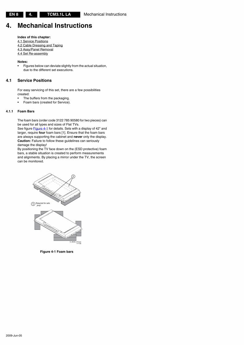
The foam bars (order code 3122 785 90580 for two pieces) can be used for all types and sizes of Flat TVs. See figure Figure 4-1 for details. Sets with a display of 42" and larger, require four foam bars [1]. Ensure that the foam bars are always supporting the cabinet and never only the display.Caution: Failure to follow these guidelines can seriously damage the display!By positioning the TV face down on the (ESD protective) foam bars, a stable situation is created to perform measurements and alignments. By placing a mirror under the TV, the screen can be monitored.
Figure 4-1 Foam bars
E_06532_018.eps171106
1
Required for sets42"
1
Mechanical Instructions EN 9TCM3.1L LA 4.
2009-Jun-05
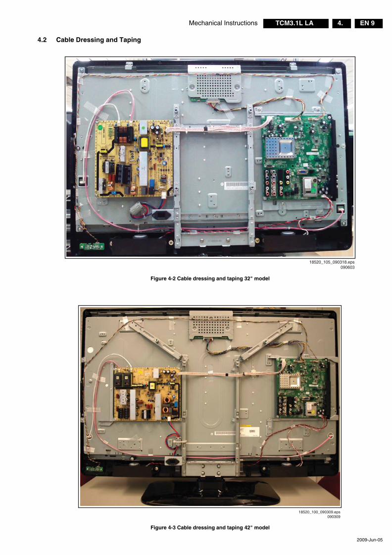
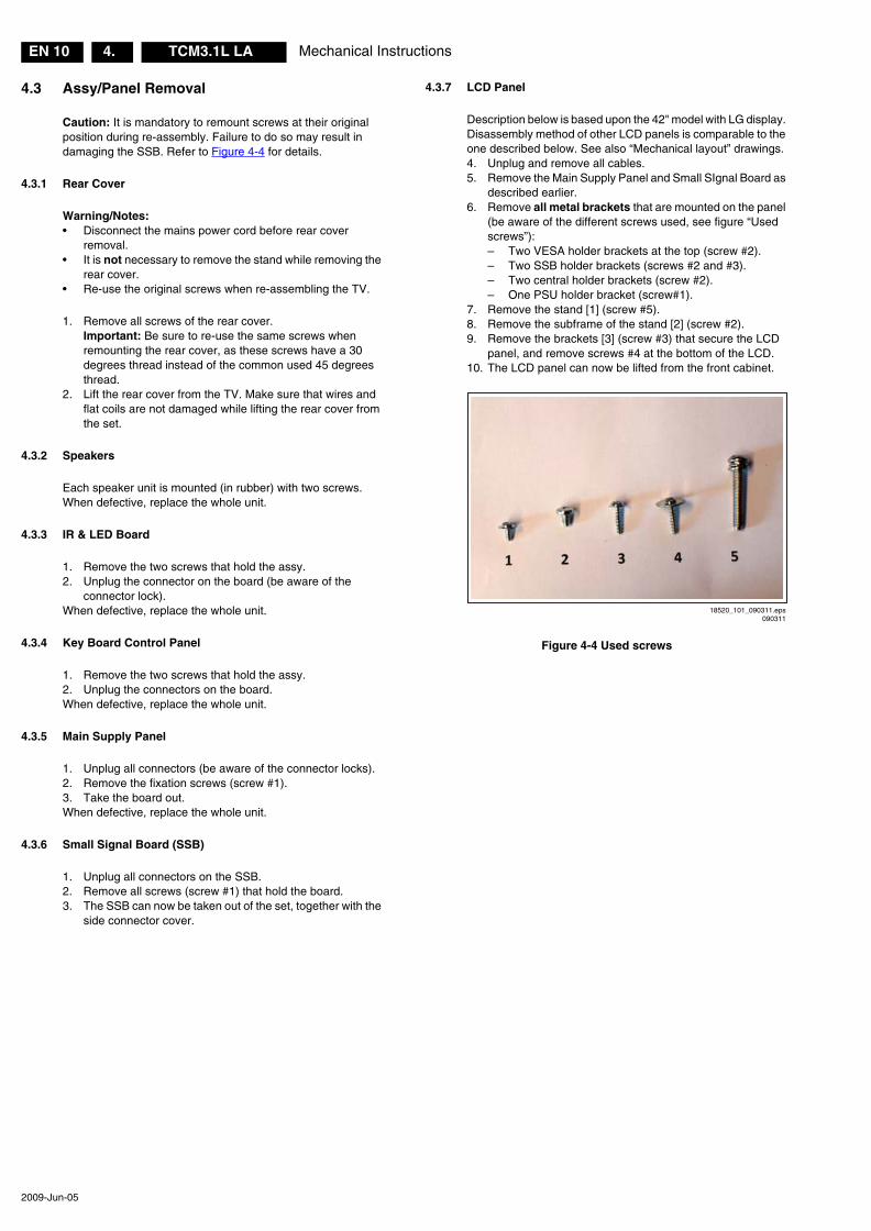
4.2 Cable Dressing and Taping
Figure 4-2 Cable dressing and taping 32" model
Figure 4-3 Cable dressing and taping 42" model
18520_105_090318.eps090603
18520_100_090309.eps090309
Mechanical InstructionsEN 10 TCM3.1L LA4.
2009-Jun-05
4.3 Assy/Panel Removal
Caution: It is mandatory to remount screws at their original position during re-assembly. Failure to do so may result in damaging the SSB. Refer to Figure 4-4 for details.
4.3.1 Rear Cover
Warning/Notes: • Disconnect the mains power cord before rear cover
removal.• It is not necessary to remove the stand while removing the
rear cover.• Re-use the original screws when re-assembling the TV.
1. Remove all screws of the rear cover. Important: Be sure to re-use the same screws when remounting the rear cover, as these screws have a 30 degrees thread instead of the common used 45 degrees thread.
2. Lift the rear cover from the TV. Make sure that wires and flat coils are not damaged while lifting the rear cover from the set.
4.3.2 Speakers
Each speaker unit is mounted (in rubber) with two screws.When defective, replace the whole unit.
4.3.3 IR & LED Board
1. Remove the two screws that hold the assy.2. Unplug the connector on the board (be aware of the
connector lock).When defective, replace the whole unit.
4.3.4 Key Board Control Panel
1. Remove the two screws that hold the assy.2. Unplug the connectors on the board.When defective, replace the whole unit.
4.3.5 Main Supply Panel
1. Unplug all connectors (be aware of the connector locks).2. Remove the fixation screws (screw #1).3. Take the board out.When defective, replace the whole unit.
4.3.6 Small Signal Board (SSB)
1. Unplug all connectors on the SSB.2. Remove all screws (screw #1) that hold the board.3. The SSB can now be taken out of the set, together with the
side connector cover.
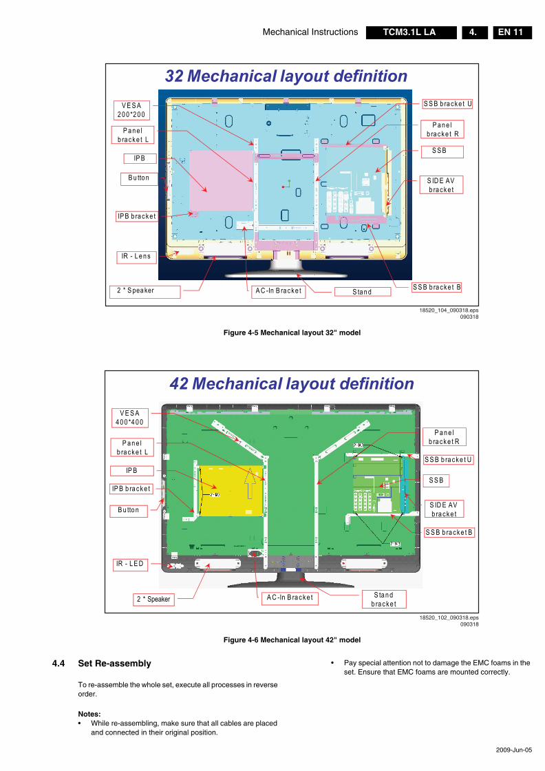
4.3.7 LCD Panel
Description below is based upon the 42" model with LG display. Disassembly method of other LCD panels is comparable to the one described below. See also “Mechanical layout” drawings.4. Unplug and remove all cables.5. Remove the Main Supply Panel and Small SIgnal Board as
described earlier.6. Remove all metal brackets that are mounted on the panel
(be aware of the different screws used, see figure “Used screws”):– Two VESA holder brackets at the top (screw #2).– Two SSB holder brackets (screws #2 and #3).– Two central holder brackets (screw #2).– One PSU holder bracket (screw#1).
7. Remove the stand [1] (screw #5).8. Remove the subframe of the stand [2] (screw #2).9. Remove the brackets [3] (screw #3) that secure the LCD
panel, and remove screws #4 at the bottom of the LCD.10. The LCD panel can now be lifted from the front cabinet.
Figure 4-4 Used screws
18520_101_090311.eps090311
Mechanical Instructions EN 11TCM3.1L LA 4.
2009-Jun-05
Figure 4-5 Mechanical layout 32" model
Figure 4-6 Mechanical layout 42" model
4.4 Set Re-assembly
To re-assemble the whole set, execute all processes in reverse order.
Notes:• While re-assembling, make sure that all cables are placed
and connected in their original position.
• Pay special attention not to damage the EMC foams in the set. Ensure that EMC foams are mounted correctly.
32 Mechanical layout definition
B u tto n S ID E AV b ra c k e t
S S B
IR - L e n s
S ta n d2 * S pea ker A C -In B ra c k e t
IP B
V E S A 2 0 0 *2 0 0
IP B b ra c k e t
P a n e l b ra c k e t L
P a n e l b ra c k e t R
S S B b ra c k e t B
S S B b ra c k e t U
18520_104_090318.eps090318
42 Mechanical layout definition
S ID E AV b ra c k e t
S S B
B u tto n
IR - L E D
S ta n d b ra c k e t2 * Speaker A C -In B ra c k e t
IP B
V E S A 4 0 0 *4 0 0
IP B b ra c k e t
P a n e l b ra c k e t L
P a n e l b ra c k e t R
S S B b ra c k e t B
S S B b ra c k e t U
18520_102_090318.eps090318
Service Modes, Error Codes, and Fault FindingEN 12 TCM3.1L LA5.
2009-Jun-05
5. Service Modes, Error Codes, and Fault Finding
Index of this chapter:5.1 Measurement Conditions5.2 Service Modes5.3 Service Tools5.4 Error Codes5.5 The Blinking LED Procedure (LAYER-2 codes)5.6 Fault Finding and Repair Tips5.7 Software Upgrading
5.1 Measurement Conditions
Perform measurements under the following conditions:• Service Default Mode.• Video: Colour bar signal.• Audio: 3 kHz left, 1 kHz right.
5.2 Service Modes
Note: For the new model range, a new remote control (RC) is used with some renamed buttons. This has an impact on the activation of the Service modes. For instance the old “MENU” button is now called “HOME” (or is indicated by a “house” icon).
Service Default mode (SDM) and Service Alignment Mode (SAM) offer several features for the service technician, while the Customer Service Mode (CSM) is used for communication between the call centre and the customer.This chassis also offers the option of using ComPair, a hardware interface between a computer and the TV chassis. It offers the abilities of structured troubleshooting, error code reading, and software version read-out for all chassis. (see also section 5.3.1 ComPair).
5.2.1 Service Default Mode (SDM)
PurposeTo start the blinking LED procedure where only layer 2 errors are displayed (see also section 5.4 Error Codes).
How to Activate SDMUse the standard RC-transmitter and key in the code “062596”, directly followed by the “MENU” (or HOME) button.After activating this mode, “SDM” will appear in the upper right corner of the screen (when a picture is available).
How to NavigateWhen the “MENU” (or HOME) button is pressed on the RC transmitter, the set will toggle between the SDM and the normal user menu (with the SDM mode still active in the background).
How to Exit SDMSwitch the set to STAND-BY via the RC-transmitter.
5.2.2 Service Alignment Mode (SAM)
Purpose• To perform (software) alignments.• To change option settings.• To easily identify the used software version.• To view operation hours.• To display (or clear) the error code buffer.
How to Activate SAMVia a standard RC transmitter: key in the code “062596” directly followed by the “i+/INFO” button.
Contents of SAM (see also 6.4 Option Settings):• Syst. Info. Giving overview of:
– Op. Hours. During the life time cycle of the TV, a life timer is kept. It counts the normal operation hours, not the Stand-by hours. The actual value of the life timer is displayed in SAM in decimal value. For every two start-ups the counter increases by one. Min. 5 digits are displayed in decimal digits. In detail:• Every 2x cold start-ups, to display a picture,
increases the counter by 1 (i.e. interrupt the mains supply 2x while the set is ON).
• Every 2x warm start-ups (from Stand-by), to display a picture, increases the counter by 1.
• Every hour of normal operating increases the counter by 1 (i.e. if a set is continue ON for 2 hours, then increase the counter by 2).
• Stand-by hours are NOT counted.– Main SW ID. Displays the loaded main SW version. – Error Code x (where “x” is 1 to 5). The most recent
error is displayed at the upper position (for an error explanation see section 5.4 Error Codes).
• Clear Codes. When “arrow right” is pressed and then the “OK” button is pressed, the error buffer is reset.
• Options. Choosing the CTN will set the options, see also chapter 6.4 Option Settings.
• RGB Align. This will activate the alignments sub-menu. See chapter 6.3.2 White Point for more details.
• NVM Editor. This will give the opportunity to directly change values in the NVM by selecting the address and value. Use decimal values! See chapter 6.4 Option Settings.
• NVM Copy. For easy transfer of NVM settings:– Copy to USB. To upload several settings from the TV
to an USB stick. See 5-1 USB Copy content. To upload the settings, press “arrow right” (or the “OK button), confirm with “OK” and wait until “OK” appears. Now the settings are stored onto the USB stick can be used to download to another TV or other SSB. Uploading is of course only possible if the software is running and if a picture is available. This method is created to be able to save the customer’s TV settings and to store them into another SSB.
– Copy from USB. To download several settings from the USB stick to the TV. Same way of working as with uploading. To make sure that the download of the channel list from USB to the TV is executed properly, it is necessary to restart the TV and tune to a valid preset if necessary.
Table 5-1 USB Copy content
S/N NVM USB Copy content To be copied /Remarks
1 Display settings White Point alignment,RGB
Yes
2 Personal settings eg. Brightness, colour,hue, equalizer, band,head phone volume, childlock, time, picture for-mat...
Yes
3 Channel List Channel preset Yes
4 Options list Option code Yes
5 AGC and AFC alignment
SSB specific No.
6 HDCP key No.
7 Model 22PFL1234D/10 Yes
8 Production serial nbr. BA1A0837123456 Yes
9 Software Version TXM21E 1.00 No. Read and display.
10 Option Code (used display)
009 yes
11 Codes 011 000 000 000 000 No. Error detection
12 SSB 996512312345 No
13 Display 996512345678 Yes
14 PSU 996512311111 Yes
15 NVM version Supplier to advise NVM version
No. Read and display.
Service Modes, Error Codes, and Fault Finding EN 13TCM3.1L LA 5.
2009-Jun-05
• Tuner. This will activate the alignments sub-menu. See chapter 6.3.1 Tuner AGC (RF AGC Take Over Point Adjustment) for more details.
• Auto ADC. This will activate the alignments sub-menu. See chapter 6.3.3 Auto ADC for more details.
How to Navigate• In SAM, the menu items can be selected with the “Arrow
up/down” key on the RC-transmitter. The selected item will be highlighted. When not all menu items fit on the screen, move the “Arrow up/down” key to display the next/previous menu items.
• With the “Arrow Left/Right” keys, it is possible to:– (De) activate the selected menu item.– (De) activate the selected sub menu.
• With the “OK” key, it is possible to activate the selected action.
• With the “Menu/Home” key, it is possible to go back to the previous selection.
How to Exit SAMSwitch the set to STAND-BY via the RC-transmitter.
5.2.3 Customer Service Mode (CSM)
PurposeWhen a customer is having problems with his TV-set, he can call his dealer or the Customer Helpdesk. The service technician can then ask the customer to activate the CSM, in order to identify the status of the set. Now, the service technician can judge the severity of the complaint. In many cases, he can advise the customer how to solve the problem, or he can decide if it is necessary to visit the customerThe CSM is a read only mode; therefore, modifications in this mode are not possible
When CSM is activated:• A test pattern will be displayed during 3 s. This test pattern
is generated by the MT822x video processor. So if this test pattern is shown, it could be determined that the back end video chain (MT822x, LVDS, and display) of the SSB is working.
• The LAYER 1 error is displayed via the blinking front LED. Only the latest error is displayed. See also section 5.4 Error Codes.
How to Activate CSMKey in the code “123654” via the standard RC transmitter. Note: Activation of the CSM is only possible if there is no (user) menu on the screen!
How to NavigateBy means of the “Arrow up/down” button on the RC-transmitter, one can navigate through the menus.
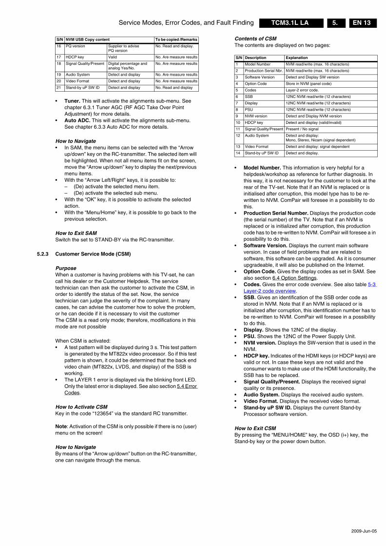
Contents of CSMThe contents are displayed on two pages:
• Model Number. This information is very helpful for a helpdesk/workshop as reference for further diagnosis. In this way, it is not necessary for the customer to look at the rear of the TV-set. Note that if an NVM is replaced or is initialised after corruption, this model type has to be re-written to NVM. ComPair will foresee in a possibility to do this.
• Production Serial Number. Displays the production code (the serial number) of the TV. Note that if an NVM is replaced or is initialized after corruption, this production code has to be re-written to NVM. ComPair will foresee a in possibility to do this.
• Software Version. Displays the current main software version. In case of field problems that are related to software, this software can be upgraded. As it is consumer upgradeable, it will also be published on the Internet.
• Option Code. Gives the display codes as set in SAM. See also section 6.4 Option Settings.
• Codes. Gives the error code overview. See also table 5-3 Layer-2 code overview.
• SSB. Gives an identification of the SSB order code as stored in NVM. Note that if an NVM is replaced or is initialized after corruption, this identification number has to be re-written to NVM. ComPair will foresee in a possibility to do this.
• Display. Shows the 12NC of the display.• PSU. Shows the 12NC of the Power Supply Unit.• NVM version. Displays the SW-version that is used in the
NVM.• HDCP key. Indicates of the HDMI keys (or HDCP keys) are
valid or not. In case these keys are not valid and the consumer wants to make use of the HDMI functionality, the SSB has to be replaced.
• Signal Quality/Present. Displays the received signal quality or its presence.
• Audio System. Displays the received audio system.• Video Format. Displays the received video format.• Stand-by uP SW ID. Displays the current Stand-by
Processor software version.
How to Exit CSMBy pressing the “MENU/HOME” key, the OSD (i+) key, the Stand-by key or the power down button.
16 PQ version Supplier to advise PQ version
No. Read and display.
17 HDCP key Valid No. Are measure results
18 Signal Quality/Present Digital percentage and analog Yes/No.
No. Are measure results
19 Audio System Detect and display No. Are measure results
20 Video Format Detect and display No. Are measure results
21 Stand-by uP SW ID Detect and display No. Read and display
S/N NVM USB Copy content To be copied /Remarks
S/N Description Explanation
1 Model Number NVM read/write (max. 16 characters)
2 Production Serial Nbr. NVM read/write (max. 16 characters)
3 Software Version Detect and Display SW version
4 Option Code Store in NVM (panel code)
5 Codes Layer-2 error code.
6 SSB 12NC NVM read/write (12 characters)
7 Display 12NC NVM read/write (12 characters)
8 PSU 12NC NVM read/write (12 characters)
9 NVM version Detect and Display NVM version
10 HDCP key Detect and display (valid/invalid)
11 Signal Quality/Present Present / No signal
12 Audio System Detect and display: Mono, Stereo, Nicam (signal dependent)
13 Video Format Detect and display: signal dependent
14 Stand-by uP SW ID Detect and display.
Service Modes, Error Codes, and Fault FindingEN 14 TCM3.1L LA5.
2009-Jun-05
5.3 Service Tools
5.3.1 ComPair
IntroductionComPair (Computer Aided Repair) is a Service tool for Philips Consumer Electronics products. and offers the following:1. ComPair helps to quickly get an understanding on how to
repair the chassis in a short and effective way.2. ComPair allows very detailed diagnostics and is therefore
capable of accurately indicating problem areas. No knowledge on I2C or UART commands is necessary, because ComPair takes care of this.
3. ComPair speeds up the repair time since it can automatically communicate with the chassis (when the uP is working) and all repair information is directly available.
4. ComPair features TV software up possibilities.
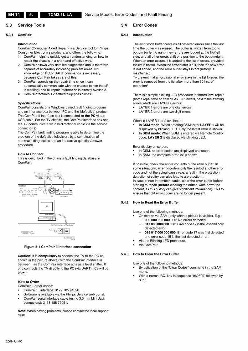
SpecificationsComPair consists of a Windows based fault finding program and an interface box between PC and the (defective) product. The ComPair II interface box is connected to the PC via an USB cable. For the TV chassis, the ComPair interface box and the TV communicate via a bi-directional cable via the service connector(s).The ComPair fault finding program is able to determine the problem of the defective television, by a combination of automatic diagnostics and an interactive question/answer procedure.
How to ConnectThis is described in the chassis fault finding database in ComPair.
Figure 5-1 ComPair II interface connection
Caution: It is compulsory to connect the TV to the PC as shown in the picture above (with the ComPair interface in between), as the ComPair interface acts as a level shifter. If one connects the TV directly to the PC (via UART), ICs will be blown!
How to OrderComPair II order codes:• ComPair II interface: 3122 785 91020.• Software is available via the Philips Service web portal.• ComPair serial interface cable (using 3.5 mm Mini Jack
connectors): 3138 188 75051. Note: When having problems, please contact the local support desk.
5.4 Error Codes
5.4.1 Introduction
The error code buffer contains all detected errors since the last time the buffer was erased. The buffer is written from top to bottom (or left to right), new errors are logged at the top/left side, and all other errors shift one position to the bottom/right.When an error occurs, it is added to the list of errors, provided the list is not full. When the error buffer is full, then the new error is not added, and the error buffer stays intact (history is maintained).To prevent that an occasional error stays in the list forever, the error is removed from the list after more than 50 hrs. of operation/
There is a simple blinking LED procedure for board level repair (home repair) the so called LAYER 1 errors, next to the existing errors which are LAYER 2 errors:• LAYER 1 errors are one digit errors• LAYER 2 errors are two digit errors.
When is LAYER 1 or 2 available:• In CSM mode: When entering CSM: error LAYER 1 will be
displayed by blinking LED. Only the latest error is shown.• In SDM mode: When SDM is entered via Remote Control
code, LAYER 2 is displayed via blinking LED.
Error display on screen:• In CSM, no error codes are displayed on screen.• In SAM, the complete error list is shown.
If possible, check the entire contents of the error buffer. In some situations, an error code is only the result of another error code and not the actual cause (e.g. a fault in the protection detection circuitry can also lead to a protection). In case of non-intermittent faults, clear the error buffer before starting to repair (before clearing the buffer, write down the content, as this history can give significant information). This to ensure that old error codes are no longer present.
5.4.2 How to Read the Error Buffer
Use one of the following methods:• On screen via SAM (only when a picture is visible). E.g.:
– 000 000 000 000 000: No errors detected– 017 000 000 000 000: Error code 17 is the last and only
detected error.– 015 017 000 000 000: Error code 17 was first detected
and error code 15 is the last detected error.• Via the Blinking LED procedure.• Via ComPair.
5.4.3 How to Clear the Error Buffer
Use one of the following methods:• By activation of the “Clear Codes” command in the SAM
menu.• With a normal RC, key in sequence “062599” followed by
“OK”.
E_06532_036.eps150208
TOUART SERVICECONNECTOR
TOUART SERVICECONNECTOR
TOI2C SERVICECONNECTOR
TO TV
PC
HDMII2C only
Optional power5V DC
ComPair II Developed by Philips Brugge
RC outRC in
OptionalSwitch
Power ModeLink/Activity I2C
ComPair IIMulti
function
RS232 /UART
Service Modes, Error Codes, and Fault Finding EN 15TCM3.1L LA 5.
2009-Jun-05
5.4.4 Error Codes
Take notice that some errors need several minutes before they start blinking or before they will be logged. So in case of problems wait 2 minutes from start-up onwards, and then check if the front LED is blinking or if an error is logged.
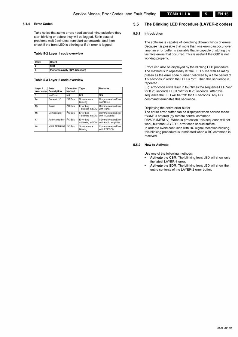
Table 5-2 Layer 1 code overview
Table 5-3 Layer-2 code overview
5.5 The Blinking LED Procedure (LAYER-2 codes)
5.5.1 Introduction
The software is capable of identifying different kinds of errors. Because it is possible that more than one error can occur over time, an error buffer is available that is capable of storing the last five errors that occurred. This is useful if the OSD is not working properly.
Errors can also be displayed by the blinking LED procedure.The method is to repeatedly let the LED pulse with as many pulses as the error code number, followed by a time period of 1.5 seconds in which the LED is “off”. Then this sequence is repeated. E.g. error code 4 will result in four times the sequence LED “on” for 0.25 seconds / LED “off” for 0.25 seconds. After this sequence the LED will be “off” for 1.5 seconds. Any RC command terminates this sequence.
Displaying the entire error bufferThe entire error buffer can be displayed when service mode “SDM” is entered (by remote control command 062596<MENU>). When in protection, this sequence will not work, but than LAYER-1 error code should suffice.In order to avoid confusion with RC signal reception blinking, this blinking procedure is terminated when a RC command is received.
5.5.2 How to Activate
Use one of the following methods:• Activate the CSM. The blinking front LED will show only
the latest LAYER-1 error.• Activate the SDM. The blinking front LED will show the
entire contents of the LAYER-2 error buffer.
Code Board
2 SSB
3 Platform supply (12V detection)
Layer 2 error code
Error Description
Detection Method
Type Remarks
0 No Error N/A N/A N/A
14 General I2C I2C Bus Spontaneous blinking
Communication Error on I2C bus
15 Tuner I2C Bus Error Log + blinking in SDM
Communication Error with Tuner
16 Demodulator I2C Bus Error Log + blinking in SDM
Communication Error with TDA9886T
17 Audio amplifier I2C Bus Error Log + blinking in SDM
Communication Error with Audio amplifier
18 NVM EEPROM I2C Bus Spontaneous blinking
Communication Error with EEPROM
Service Modes, Error Codes, and Fault FindingEN 16 TCM3.1L LA5.
2009-Jun-05
5.6 Fault Finding and Repair Tips
5.6.1 Fault Finding Flow Charts
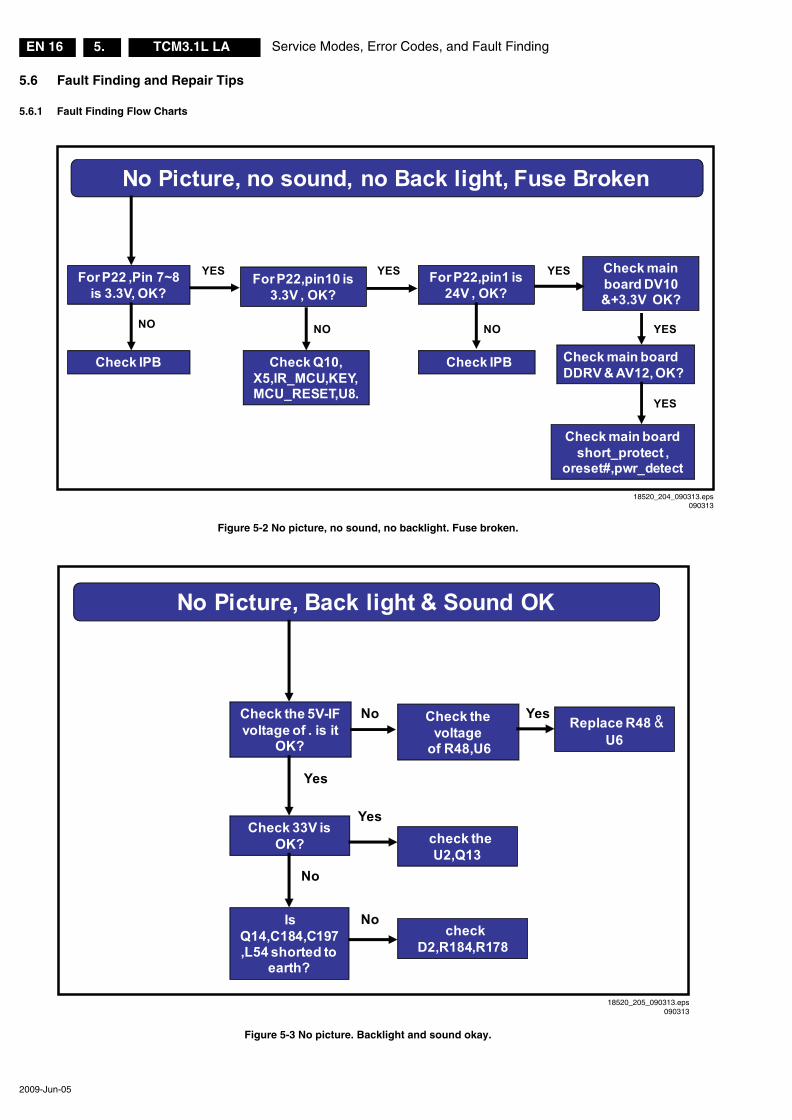
Figure 5-2 No picture, no sound, no backlight. Fuse broken.
Figure 5-3 No picture. Backlight and sound okay.
18520_204_090313.eps090313
No Picture, no sound, no Back light, Fuse Broken
For P22,pin10 is 3.3V , OK?
For P22,pin1 is 24V , OK?
Check IPB
For P22 ,Pin 7~8 is 3.3V, OK?
Check Q10, X5,IR_MCU,KEY,MCU_RESET,U8.
Check main board DV10 &+3.3V OK?
NO NO NO
YES YES YES
Check main board DDRV & AV12, OK?
YES
Check main board short_protect ,
oreset#,pwr_detect
YES
Check IPB
18520_205_090313.eps090313
No Picture, Back light & Sound OK
Check the 5V-IF voltage of . is it
OK?
Check 33V is OK?
Check the voltage
of R48,U6
Yes
No
Yes
Is Q14,C184,C197 ,L54 shorted to
earth?
Replace R48 &U6
Yes
No
check the U2,Q13
check D2,R184,R178
No
Service Modes, Error Codes, and Fault Finding EN 17TCM3.1L LA 5.
2009-Jun-05
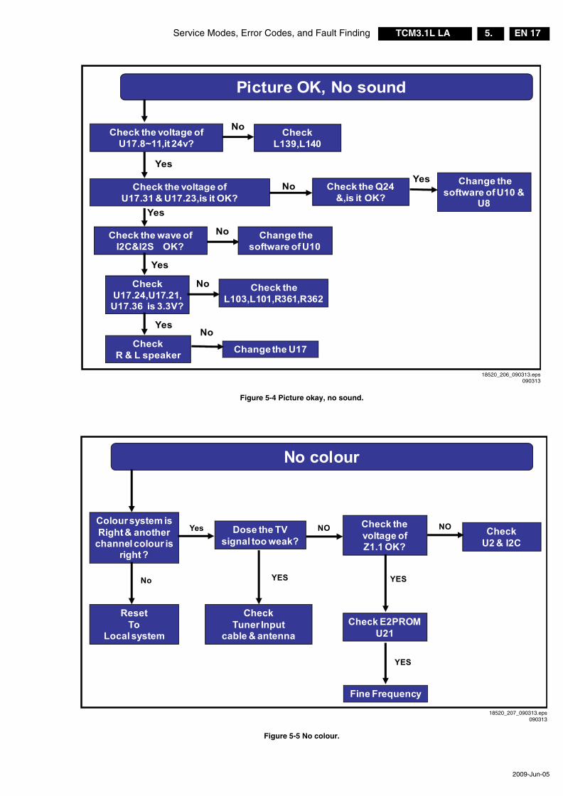
Figure 5-4 Picture okay, no sound.
Figure 5-5 No colour.
18520_206_090313.eps090313
Picture OK, No sound
Check the voltage ofU17.8~11,it 24v?
Check L139,L140
Check the Q24 &,is it OK?
Change the software of U10 &
U8
Change the U17
CheckU17.24,U17.21,U17.36 is 3.3V?
No
Check the wave ofI2C&I2S OK?
YesCheck the voltage of
U17.31 & U17.23,is it OK?
Yes
Yes
Yes
No
Yes
No
NoCheck
R & L speaker
No Change the software of U10
Check the L103,L101,R361,R362
18520_207_090313.eps090313
No colour
Colour system is Right & another
channel colour is right ?
Dose the TV signal too weak?
Check the voltage ofZ1.1 OK?
CheckU2 & I2C
ResetTo
Local system
Check Tuner Input
cable & antennaCheck E2PROM
U21
Yes NO NO
No YES YES
Fine Frequency
YES
Service Modes, Error Codes, and Fault FindingEN 18 TCM3.1L LA5.
2009-Jun-05
5.7 Software Upgrading
5.7.1 Introduction
It is possible for the user to upgrade the main software via the USB port. A description on how to upgrade the main software can be found in the DFU and below.
5.7.2 Main Software Upgrade
In “normal” conditions, so when there is no major problem with the TV, the main software and the default software upgrade application can be upgraded with the “upgrade.bin”. This can also be done by the consumers themselves via the Software Update Assistant in the user menu (see DFU), but they will have to download their software from the commercial Philips website.
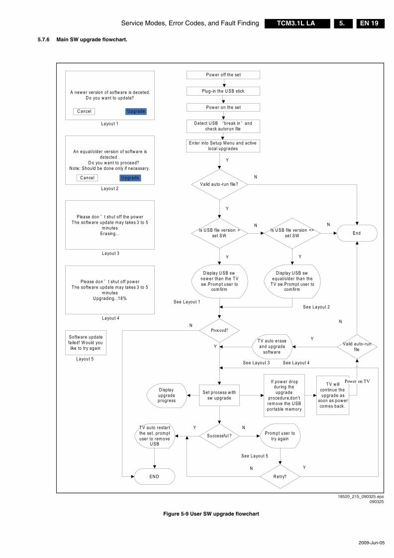
How to upgrade (see also figure 5-9 User SW upgrade flowchart):1. Copy the “upgrade.bin” file to the root of the USB stick.2. Power “off” the TV and remove all memory devices.3. Insert the USB stick that contains the downloaded software
upgrade.4. Switch “on” the TV, and activate the Main menu with the
“Menu/House” key on the remote control.5. In the Main menu, go to the “Software update” item.6. Press “OK” key to go to the submenu. 7. Select “Local updates” in the submenu and press the “OK”
key to enter the Software Update application.8. You will be prompted to cancel or to proceed with the
software updating.9. To proceed, select “Update” and press the “OK” key to
enter the next menu. In the next menu select “Start” and press “OK” key to start the software update.
10. Upgrading will now begin and the progress of the updating will be displayed. After the software updating is completed, the TV will automatically restart.
5.7.3 Stand-by Software Upgrade
In this chassis it is not possible to upgrade the Stand-by software via a USB stick or ComPair. Please order a pre-programmed device via the Philips Spare Part web portal.
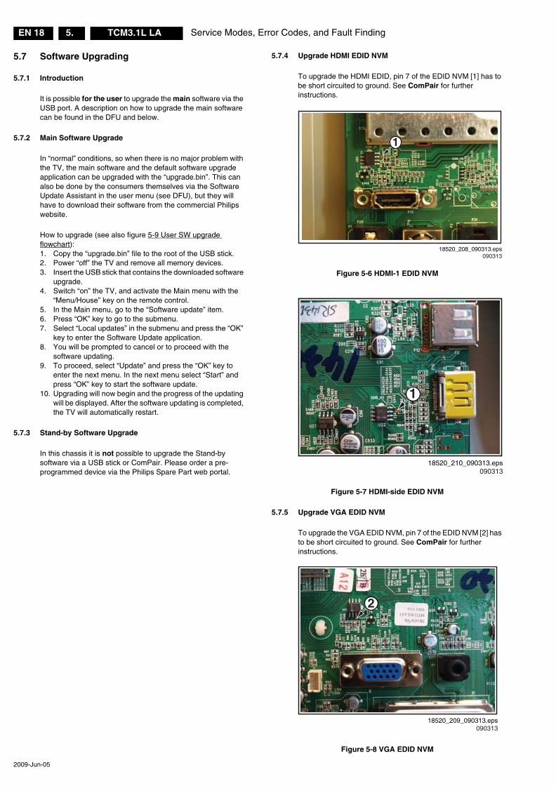
5.7.4 Upgrade HDMI EDID NVM
To upgrade the HDMI EDID, pin 7 of the EDID NVM [1] has to be short circuited to ground. See ComPair for further instructions.
Figure 5-6 HDMI-1 EDID NVM
Figure 5-7 HDMI-side EDID NVM
5.7.5 Upgrade VGA EDID NVM
To upgrade the VGA EDID NVM, pin 7 of the EDID NVM [2] has to be short circuited to ground. See ComPair for further instructions.
Figure 5-8 VGA EDID NVM
18520_208_090313.eps090313
1
18520_210_090313.eps090313
1
18520_209_090313.eps090313
2
Service Modes, Error Codes, and Fault Finding EN 19TCM3.1L LA 5.
2009-Jun-05
5.7.6 Main SW upgrade flowchart.
Figure 5-9 User SW upgrade flowchart
18520_215_090325.eps090325
A new er version of softw are is deceted.D o you w ant to update?
U pgradeC ancel
An equal/o lder version of softw are is detected .
D o you w ant to proceed?N ote: Should be done only if necessary .
U pgradeC ancel
Layout 1
Layout 2
Pow er off the set
Plug- in the U SB stick
Enter in to Setup M enu and active local upgrades
Valid auto -run file?
Is U SB file version > set SW
Is U SB file version <= set SW End
Y
N
Y
N
N
D isplay U SB sw new er than the T V sw .Prom pt user to
com firm
Y
D isplay U SB sw equal/o lder than the
T V sw.Prom pt user to com firm
Y
Pow er on the set
D etect U SB break in and check autorun file
Please don t shut off the pow er T he softw are update m ay takes 3 to 5
m inutesErasing...
P lease don t shut off pow erT he softw are update m ay takes 3 to 5
m inutesU pgrading...18%
Layout 3
Layout 4
Proceed?
See Layout 1See Layout 2
Set process w ith sw upgrade
Successfu l ?T V auto restar t the set, prom pt user to rem ove
U SB
N
EN D
Y
If pow er drop dur ing the upgrade
procedure,don’t rem ove the U SB por table m em ory
T V w ill continue the upgrade as
soon as pow er com es back .
See Layout 3 See Layout 4
Power on TV
Valid auto- run file
Y
N
T V auto erase and upgrade
softw are
D isplay upgrade progress
Y NProm pt user to
try again
Softw are update fa iled! W ould you like to try again
Layout 5
See Layout 5
R etry?N Y
AlignmentsEN 20 TCM3.1L LA6.
2009-Jun-05
6. Alignments
Index of this chapter:6.1 General Alignment Conditions6.2 Hardware Alignments6.3 Software Alignments6.4 Option Settings6.5 Reset of Repaired SSB
6.1 General Alignment Conditions
Perform all electrical adjustments under the following conditions:• Power supply voltage (depends on region):
– AP-NTSC: 120 VAC or 230 VAC / 50 Hz (± 10%).– AP-PAL-multi: 120 - 230 VAC / 50 Hz (± 10%).– EU: 230 VAC / 50 Hz (± 10%).– LATAM-NTSC: 120 - 230 VAC / 50 Hz (± 10%).– US: 120 VAC / 60 Hz (± 10%).
• Connect the set to the mains via an isolation transformer with low internal resistance.
• Allow the set to warm up for approximately 15 minutes.• Measure voltages and waveforms in relation to correct
ground (e.g. measure audio signals in relation to AUDIO_GND). Caution: It is not allowed to use heat sinks as ground.
• Test probe: Ri > 10 MΩ, Ci < 20 pF.• Use an isolated trimmer/screwdriver to perform
alignments.
6.1.1 Alignment Sequence
• First, set the correct options: see also section Option codes• Warming up (>15 minutes).• Start the alignments.
6.2 Hardware Alignments
Not applicable.
6.3 Software Alignments
Put the set in SAM mode (see chapter 5. Service Modes, Error Codes, and Fault Finding). The SAM menu will now appear on the screen. Select the appropriate alignment and go to one of the sub menus with the “arrow right” button. The alignments are explained below.The following items can be aligned:• Tuner AGC.• White point.• ADC calibration of VGA and YPbPr inputs. To store the data:• When displayed, select “Store” in the related sub menu and
press the “OK” button on the RC. Screen text will change from “DO” to “OK”
• Press the MENU/House button on the RC.• Switch the set to Stand-by mode. For the next alignments, supply the following test signals via a video generator to the RF input:• EU/AP-PAL models: a PAL B/G TV-signal with a signal
strength of at least 1 mV and a frequency of 475.25 MHz• US/AP-NTSC models: an NTSC M/N TV-signal with a
signal strength of at least 1 mV and a frequency of 61.25 MHz (channel 3).
• LATAM models: an NTSC M TV-signal with a signal strength of at least 1 mV and a frequency of 61.25 MHz (channel 3).
6.3.1 Tuner AGC (RF AGC Take Over Point Adjustment)
Purpose: To keep the tuner output signal constant as the input signal amplitude varies.
The AGC alignment is done automatically (standard value: “12”). Store settings and exit SAM
6.3.2 White Point
• Press the “Menu/Home” button on the RC, and then select “Picture”. Set the picture settings as follows:
• Activate SAM mode and select “RGB Align”.
White point alignment LCD screens:• Use a 100% white screen on HDMI-1 as input signal and
set the following values:– “Colour temperature”: “Cool”.– All “R/G/B_Gain” values to: “127”.– All “R/G/B_Offset” values to: “240”.
In case colour analyser can be used:• Measure with a calibrated contactless colour analyser in
the centre of the screen. Consequently, the measurement needs to be done in a dark environment.
• Adjust the correct x,y coordinates by means of decreasing the value of one or two other white points to the correct x,y coordinates (see Table 6-1). Tolerance dx, dy: ± 0.004.Only the “Cool” colour temperature needs to adjust.
• When finished, select “Store” in the “RGB Align” sub menu, and press “OK” on the RC to store the aligned values to the NVM.
• Restore the initial picture settings after the alignments.
Table 6-1 White D alignment values
In case no colour analyser is available, the default values can be used. This is the next best solution. The default values are average values coming from production.• Select the “Cool” colour temperature.• Set the RED, GREEN and BLUE default values according
to the values in the “White tone default settings” table.• When finished, select “Store” in the “RGB Align” sub menu,
and press “OK” on the RC to store the aligned values to the NVM.
• Restore the initial picture settings after the alignments.
Table 6-2 White tone default settings
(*) Default values were not available at the time of publishing. They will be published as soon as they become available.
Picture Setting
Smart Picture Personal
Colour Temperature Cool
Dynamic Contrast Off
Dynamic Backlight Off
Colour Enhancement Off
Light Sensor Off
Value Cool (11000K) Normal (9000K) Warm (6500K)
x 0.278 0.289 0.314
y 0.278 0.291 0.319
White Tone 32" 42"
Colour Temp R G B R G B
Normal auto adjusted
Cool 175 151 168 176 150 170
Warm auto adjusted
Alignments EN 21TCM3.1L LA 6.
2009-Jun-05
6.3.3 Auto ADC
Purpose: For correct gray- and colour scale values of the VGA and YPbPr inputs.
How to align the VGA/PC input: 1. Provide a 1024 × 768 @ 60 Hz test signal with White/
Black squares to the VGA input.2. Select “Auto ADC” in the SAM menu.3. Press the “Arrow right” button on the RC.4. Press “OK” on the RC.5. Wait until OSD shows “Auto ADC - OK”.
How to align the YPbPr inputs (CVI-1 and CVI-2): 1. Provide a 1024 × 768 @ 60 Hz test signal with 100% 8
step colour bar to the YPbPr input.2. Rest is the same as for the VGA input.
6.4 Option Settings
6.4.1 Introduction
The microprocessor communicates with a large number of I2C ICs in the set. To ensure good communication and to make digital diagnosis possible, the microprocessor has to know which ICs to address, and what brand and type of display is used.
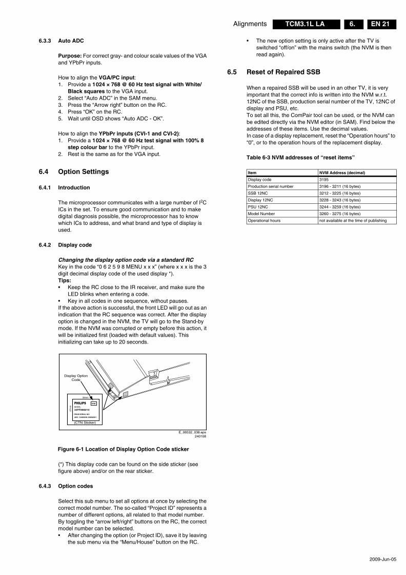
6.4.2 Display code
Changing the display option code via a standard RCKey in the code “0 6 2 5 9 8 MENU x x x” (where x x x is the 3 digit decimal display code of the used display *). Tips: • Keep the RC close to the IR receiver, and make sure the
LED blinks when entering a code.• Key in all codes in one sequence, without pauses.If the above action is successful, the front LED will go out as an indication that the RC sequence was correct. After the display option is changed in the NVM, the TV will go to the Stand-by mode. If the NVM was corrupted or empty before this action, it will be initialized first (loaded with default values). This initializing can take up to 20 seconds.
Figure 6-1 Location of Display Option Code sticker
(*) This display code can be found on the side sticker (see figure above) and/or on the rear sticker.
6.4.3 Option codes
Select this sub menu to set all options at once by selecting the correct model number. The so-called “Project ID” represents a number of different options, all related to that model number.By toggling the “arrow left/right” buttons on the RC, the correct model number can be selected.• After changing the option (or Project ID), save it by leaving
the sub menu via the “Menu/House” button on the RC.
• The new option setting is only active after the TV is switched “off/on” with the mains switch (the NVM is then read again).
6.5 Reset of Repaired SSB
When a repaired SSB will be used in an other TV, it is very important that the correct info is written into the NVM w.r.t. 12NC of the SSB, production serial number of the TV, 12NC of display and PSU, etc.To set all this, the ComPair tool can be used, or the NVM can be edited directly via the NVM editor (in SAM). Find below the addresses of these items. Use the decimal values.In case of a display replacement, reset the “Operation hours” to “0”, or to the operation hours of the replacement display.
Table 6-3 NVM addresses of “reset items”
PHILIPSMODEL:32PF9968/10
PROD.SERIAL NO:
AG 1A0620 000001
040
39mm
27m
m
(CTN Sticker)
Display OptionCode
E_06532_038.eps240108
Item NVM Address (decimal)
Display code 3195
Production serial number 3196 - 3211 (16 bytes)
SSB 12NC 3212 - 3225 (16 bytes)
Display 12NC 3228 - 3243 (16 bytes)
PSU 12NC 3244 - 3259 (16 bytes)
Model Number 3260 - 3275 (16 bytes)
Operational hours not available at the time of publishing
Circuit DescriptionsEN 22 TCM3.1L LA7.
2009-Jun-05
7. Circuit Descriptions
Index of this chapter:7.1 Introduction7.3 Power Supply7.2 Video and Audio Processing - MT822x
Notes: • Only new circuits (circuits that are not published recently)
are described. • Figures can deviate slightly from the actual situation, due
to different set executions.• For a good understanding of the following circuit
descriptions, please use the wiring, block (see chapter 9. Block Diagrams) and circuit diagrams (see chapter 10. Circuit Diagrams and PWB Layouts). Where necessary, a separate drawing for clarification is given.
7.1 Introduction
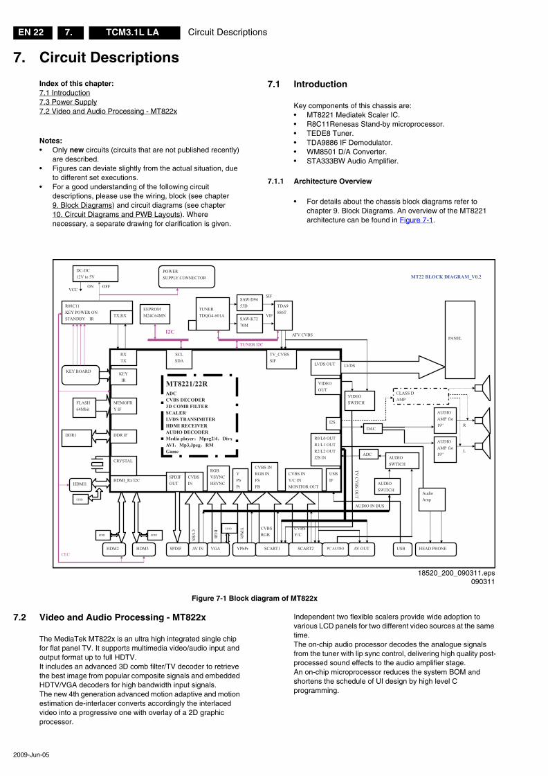
Key components of this chassis are:• MT8221 Mediatek Scaler IC.• R8C11Renesas Stand-by microprocessor.• TEDE8 Tuner.• TDA9886 IF Demodulator.• WM8501 D/A Converter.• STA333BW Audio Amplifier.
7.1.1 Architecture Overview
• For details about the chassis block diagrams refer to chapter 9. Block Diagrams. An overview of the MT8221 architecture can be found in Figure 7-1.
Figure 7-1 Block diagram of MT822x
7.2 Video and Audio Processing - MT822x
The MediaTek MT822x is an ultra high integrated single chip for flat panel TV. It supports multimedia video/audio input and output format up to full HDTV. It includes an advanced 3D comb filter/TV decoder to retrieve the best image from popular composite signals and embedded HDTV/VGA decoders for high bandwidth input signals.The new 4th generation advanced motion adaptive and motion estimation de-interlacer converts accordingly the interlaced video into a progressive one with overlay of a 2D graphic processor.
Independent two flexible scalers provide wide adoption to various LCD panels for two different video sources at the same time. The on-chip audio processor decodes the analogue signals from the tuner with lip sync control, delivering high quality post-processed sound effects to the audio amplifier stage.An on-chip microprocessor reduces the system BOM and shortens the schedule of UI design by high level C programming.
ATV CVBS
TUNER I2C
TV C
VB
S OU
T
AUDIO IN BUS
CEC
VCC
VIF
SIFSAW-D9453D
OFFON
HDMI1
HDM2
EDID
EDID
VGA
EDID
YPbPr SCART1 AV IN SPDIF
PANEL
LVDS
TUNERTDQG4-601A
SAW-K7270M
TDA9886T
FLASH64Mbit
TV_CVBSSIF
SCLSDA
I2C
R08C11 KEY POWER ON STANDBY IR
KEY BOARD KEYIR
EEPROMM24C64MN
DC-DC12V to 5V
POWER SUPPLY CONNECTOR MT22 BLOCK DIAGRAM_V0.2
SCART2
CVBSY/C
RG
B
YPbPr
CVBSRGB
HDM3
EDID
CV
BS
AV OUT PC AUDIO
VIDEOSWITCH
CVBS IN Y/C IN MONITOR OUT
CVBS IN RGB IN FSFB
YPbPr
RGBVSYNCHSYNC
CVBSIN
SPDIF OUT
HDMI_Rx I2C
R0/L0 OUT R1/L1 OUT R2/L2 OUT I2S IN
I2S
VIDEOOUT
LVDS OUT
MT8221/22RADCCVBS DECODER 3D COMB FILTER SCALER LVDS TRANSIMITER HDMI RECEIVER AUDIO DECODER Media player Mpeg2/4 DivxAVI Mp3,Jpeg RMGame
CRYSTAL
MEMOFRY IF
DDR IF
USB
USBIF
AUDIO SWITCH
AUDIO SWTICH
RXTX
TX,RX
DDR1
ADC
AUDIO AMP for 19” R
L
CLASS D AMP
AUDIO AMP for 19”
Audio Amp
DAC
HEAD PHONE
18520_200_090311.eps090311
Circuit Descriptions EN 23TCM3.1L LA 7.
2009-Jun-05
7.3 Power Supply
All power supplies used in this chassis are a “black box” for Service. When defective, a new board must be ordered and the defective one must be returned, unless the main fuse of the board is broken. Always replace a defective fuse with one with the correct specifications! This part is available in the regular market.
Consult the Service Spare Part portal for the order codes of these boards.
Below some background info on the PSUs is given, to ease the troubleshooting process in case of power supply problems
7.3.1 Diversity
The only type of power supply used in this platform is the Integrated Power Board (IPB) - incl. LCD backlight inverters.
Below find an overview of the different PSUs that are used:
Table 7-1 Supply diversity
It should be noted that for different display manufacturers, different PSUs can be used. When ordering a new PSU, always check which LCD panel is used in the set, and order the correct PSU!
7.3.2 IPL32L PSU
Block Diagram
Figure 7-2 Block diagram IPL32L PSU
Key ComponentsThe key component ICs are:• Stand-by power supply IC: FSQ510 (Fairchild).• PFC control IC: L6563 (ST).• 24V PWM control IC: FA5571N (FUJI).• Inverter high voltage control IC: OZ9976 (O2).
Control Signals
Table 7-2 Control signals
Output Characteristics
Table 7-3 Output characteristics
Fault Finding
Figure 7-3 Fault finding diagram IPL32L PSU
Supplier PSU Model Input Voltage Range
TCL
IPL32L 32" LG display
100 - 240 VacIPL42AIPL42L
42" AUO display42" LG display
Control signal Comments Output
PS-ON 3.3V >= ON >= 2.0V AC power output ON
0.7V >= OFF >= 0V AC power output OFF
BL_ON 5.0V >= ON >= 2.0V The inverter is working
1.0V >= OFF >= 0V The inverter is switched OFF
DIMP High level: 2V ~ 5.0V HD: OPC dimming, 140Hz
Low level: 0V ~ 0.7V FHD: PWM, 103.4Hz
Output Voltage Tolerance Min. current Max. current Load regulation
+3V3(STB) +/- 3% 5 mA 200 mA +/- 5%
24V +/- 5% 0.2 A 2.0 A +/- 5%
18520_211_090319.eps090319
E MCFilter circu it
B ridge rectif ier F ilter circu it
P FC C ircu itIC 1L1
P W MC ircu it
IC 2T1
3 .3V
Feedback circu it P rotection circu it
S tan dby circu it
IC 3 / T2
T4H V tran s form er
IN V E R TE R C on tro l an d drive circu it
A C IN
BL-ON
H igh Voltage A C ou tpu t
B ridge rectif ier F ilter circu it
MC U
12V R elay K 1 Optocou pler
24V
S tartup S ig na l
C ircu it
V CC
12V o p erat ing vo ltag e
PDIM
PS - ON
395V
18520_212_090319.eps090319
3.3V no rm a l?
S witch “o n”
P S _ON no rm a l?
Relay is c lo sed ?
P FC vo ltag e no rm a l?
Y
Y
Y
Y
N
N
N
N
CB 1 vo ltag e no rm a l?
P FC_V CC no rm a l?
N24V no rm a l?
Fau lt m o vem ent
Relay p o wer sup p ly p art (QB 1) f au lt
B L_ON and D IM P normal?
NFau lt m o vem ent
Check S tand b y IC, f eed b ack, trans f o rm er f a ilures , etc .
N
Y
Fuse is o p en W hether the b rid g e rec tif ier
c ircu it
P FC IC, f eed b ack, drive f a ilure, etc .
YP FC p o wer sup p ly part (QW 11) fau lt
Y
P W M IC, f eed b ack, trans f o rm er f a ilures, etc .
N
Y
A ttentio n : a lso check the P FC and P W M co ntro l,
sho rt-c ircu it in o rd er to rep lace the Fuse and
B rid g e.
Y
HV p art f a ilure (IC p ro tec tio n circuit).
such as whether the MOS
Circuit DescriptionsEN 24 TCM3.1L LA7.
2009-Jun-05
7.3.3 IPL42L PSU
Block Diagram
Figure 7-4 Block diagram IPL42L PSU
Key ComponentsThe key component ICs are:• Stand-by power supply IC: FSQ510 (Fairchild).• PFC control IC: L6562 (ST).• 24V PWM control IC: FA5571N (FUJI).• Inverter high voltage control IC: OZ9926 (O2).
Control Signals
Table 7-4 Control signals
Output Characteristics
Table 7-5 Output characteristics
Fault FindingNormal PSU working order: • Connect the 220V AC power plug.• The 3.3V Stand-by power supply (Stand-by uP U801) will
start. This is a “single-ended flyback regulator”. For a good functioning of this part, check the availability of 1.25V on U803 (TL431).
• On connector P802, signal line “PS_ON” will go “high” (3V3) and relay K801 will be activated.
• Also capacitors C811/C812 will be charged, supplying IC806 with electricity. This will start the PFC circuit and generate the +24 V control.
• Now, IC805 will start, and will generated the 24V output.• On connector P802, signal “DIM” sets the PWM dimming
status.• On connector P802, when signal “BL-ON” goes “high”, the
high voltage Inverter (IC901, OZ9926A) will start.
Control signal Comments Output
PS-ON 5.0V >= ON >= 2.0V AC power output ON
1.0V >= OFF >= 0V AC power output OFF
BL_ON 5.0V >= ON >= 2.0V The inverter is working
1.0V >= OFF >= 0V The inverter is switched OFF
Burst dimming freq. / duty 100 - 200 Hz / 10 - 100%
PWM Dimming High level: 2V ~ 5.0V
Low level: 0V ~ 0.7V
Output Voltage Tolerance Min. current Max. current Load regulation
+3V3 +/- 5% 5 mA 300 mA +/- 5%
24V +/- 5% 0.5 A 2.5 A +/- 5%
18520_214_090319.eps090319
PFC IC L6562A
(ST)
INVERTER IC OZ9926A
(O2)
+H V
-H V
PW M Power Supply IC FA5571 (FUJI)
STB Power Supply IC FSQ 510
(FAIRCHILD
3 .3V
24V
D IM
B L-ON
P S -ON
AC Inpu t
Sw itch con tro l Vo ltage D etec t
E NA B LE
PFC ou tpu t 395V
Relay
IC Data Sheets EN 25TCM3.1L LA 8.
2009-Jun-05
8. IC Data Sheets
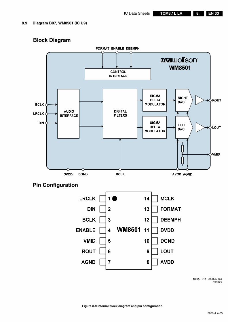
Index of this chapter:8.1 Diagram B01, LD1117 (IC U4)8.2 Diagram B01, RT8110 (IC U13)8.3 Diagram B01, MP1593 (IC U14)8.4 Diagram B01, PQ1CX41 (IC U20)8.5 Diagram B02, MX25L3205 (IC U10)8.6 Diagram B02, MT8221 (IC U11)8.7 Diagram B03, RT9199 (IC U1)8.8 Diagram B04, TDA9885 (IC U2)8.9 Diagram B07, WM8501 (IC U9)8.10 Diagram B09, RC4558 (IC U26/U37)8.11 Diagram B09, LM833D (IC U27)8.12 Diagram B10, STA333BW (IC U17)
This chapter shows the internal block diagrams and pin configurations of ICs that are drawn as “black boxes” in the electrical diagrams (with the exception of “memory” and “logic” ICs).
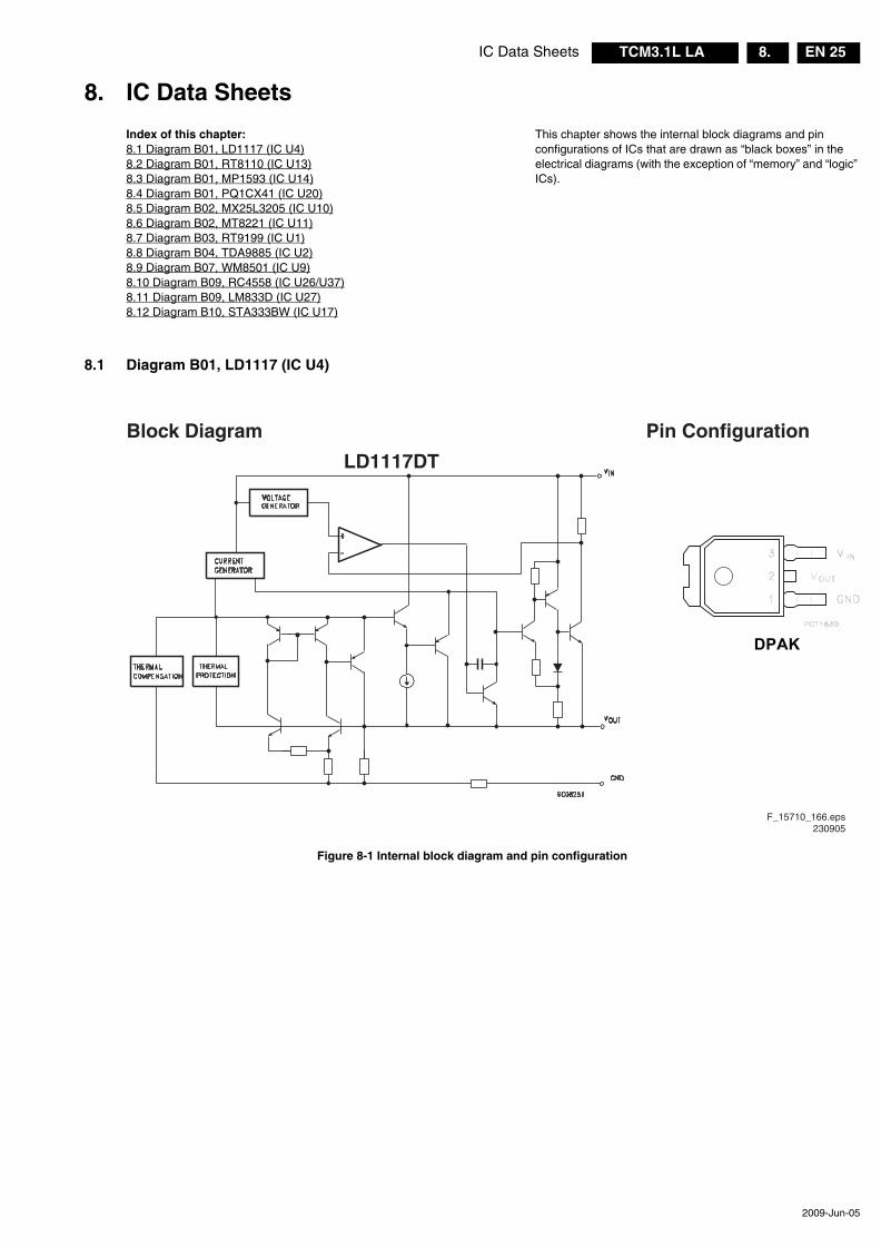
8.1 Diagram B01, LD1117 (IC U4)
Figure 8-1 Internal block diagram and pin configuration
Block Diagram Pin Configuration
F_15710_166.eps230905
LD1117DT
DPAK
IC Data SheetsEN 26 TCM3.1L LA8.
2009-Jun-05
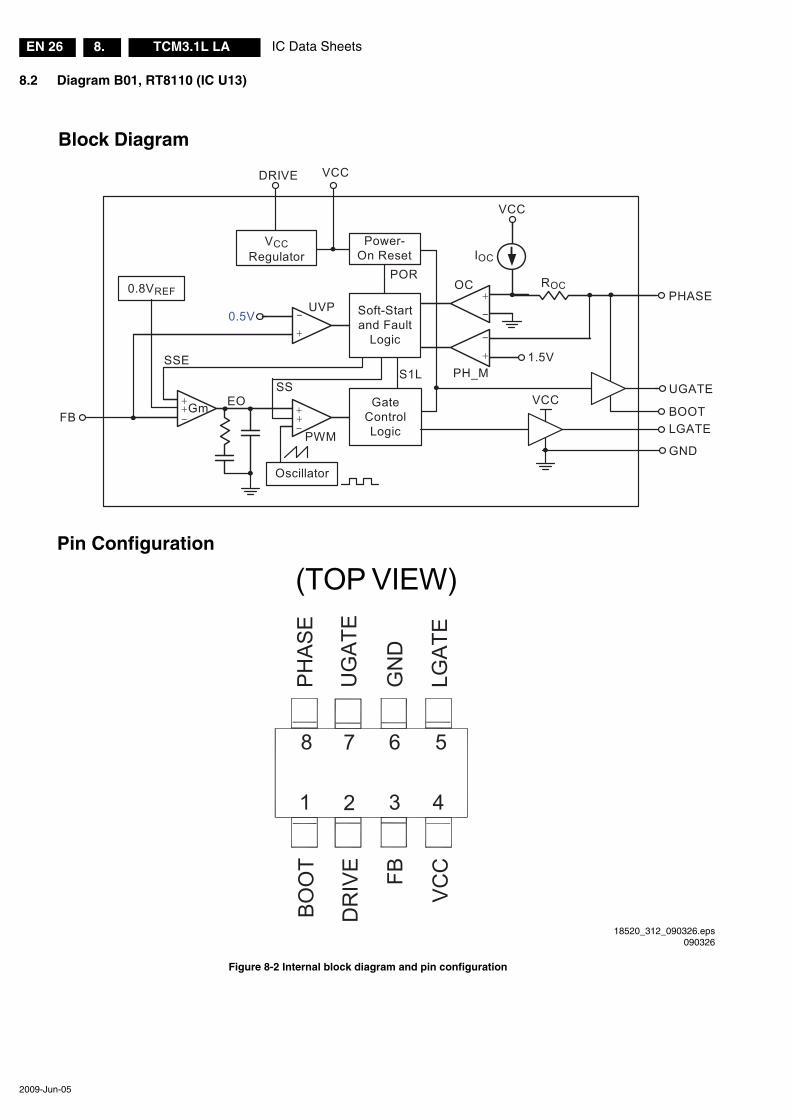
8.2 Diagram B01, RT8110 (IC U13)
Figure 8-2 Internal block diagram and pin configuration
Block Diagram
Pin Configuration
18520_312_090326.eps090326
(TOP VIEW)
BOO
T
FB
VCC
PHAS
E
GN
D
LGAT
E
DR
IVE
UG
ATE
5
3 4
68
1 2
7
Soft-Start and Fault
Logic
Gate Control Logic
+-
+-
VCC
ROC
IOC
1.5V
BOOTFB
VCC
PHASE
GND
LGATE
DRIVE
UGATEVCC
Power-On Reset
POR
+-0.5V
+-+
+-+
0.8VREF
UVP
PWM
Gm
VCCRegulator
Oscillator
S1L
OC
PH_MSSE
EOSS
IC Data Sheets EN 27TCM3.1L LA 8.
2009-Jun-05
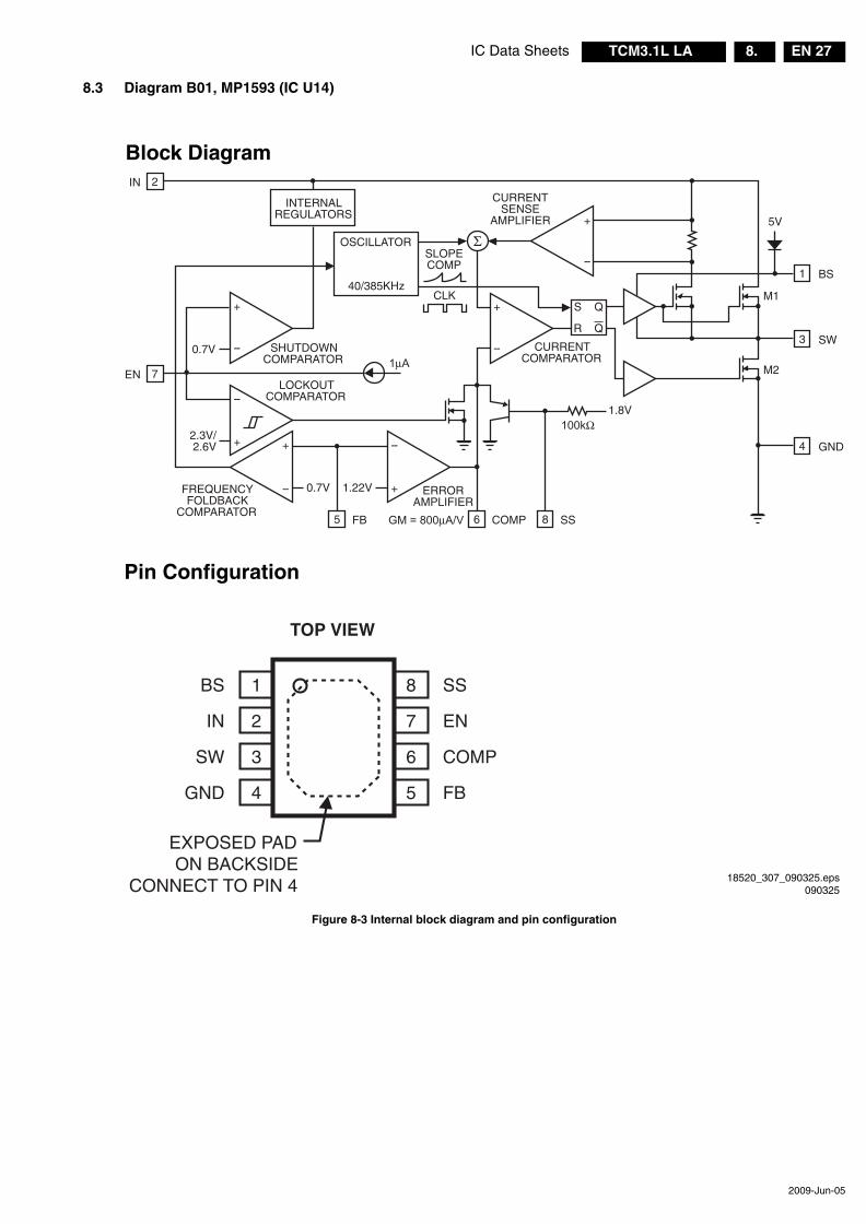
8.3 Diagram B01, MP1593 (IC U14)
Figure 8-3 Internal block diagram and pin configuration
Block Diagram
Pin Configuration
18520_307_090325.eps090325
BS
IN
SW
GND
SS
EN
COMP
FB
1
2
3
4
8
7
6
5
TOP VIEW
EXPOSED PADON BACKSIDE
CONNECT TO PIN 4
LOCKOUTCOMPARATOR
ERRORAMPLIFIER
FREQUENCYFOLDBACK
COMPARATOR
INTERNALREGULATORS
1.8V
SLOPECOMP
CLK
CURRENTCOMPARATOR
CURRENTSENSE
AMPLIFIER
SHUTDOWNCOMPARATOR
SS8COMP6
IN 2
EN 7
GND4
OSCILLATOR
40/385KHz
S
R
Q
SW3
BS
M1
M2
1
5V+
Q
0.7V
+ +
2.3V/2.6V +
1.22V0.7V +
+
FB5
--
--
--
--
--
--
IC Data SheetsEN 28 TCM3.1L LA8.
2009-Jun-05
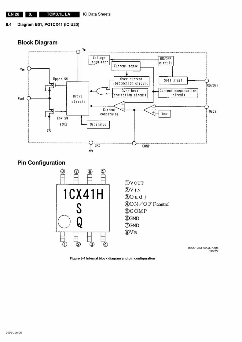
8.4 Diagram B01, PQ1CX41 (IC U20)
Figure 8-4 Internal block diagram and pin configuration
Block Diagram
Pin Configuration
18520_313_090327.eps090327
IC Data Sheets EN 29TCM3.1L LA 8.
2009-Jun-05
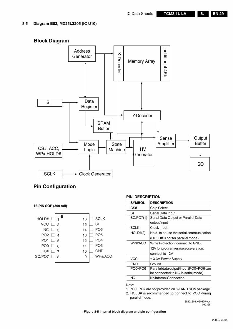
8.5 Diagram B02, MX25L3205 (IC U10)
Figure 8-5 Internal block diagram and pin configuration
Block Diagram
Pin Configuration
18520_308_090325.eps090325
SYMBOL DESCRIPTIONCS# Chip SelectSI Serial Data InputSO/PO7(1) Serial Data Output or Parallel Data
output/inputSCLK Clock InputHOLD#(2) Hold, to pause the serial communication
(HOLD# is not for parallel mode)WP#/ACC Write Protection: connect to GND;
12V for program/erase acceleration:connect to 12V
VCC + 3.3V Power SupplyGND GroundPO0~PO6 Parallel data output/input (PO0~PO6 can
be connected to NC in serial mode)NC No Internal Connection
PIN DESCRIPTION
16-PIN SOP (300 mil)
Note:1. PO0~PO7 are not provided on 8-LAND SON package.2. HOLD# is recommended to connect to VCC during
parallel mode.
1
2
3
4
5
6
7
8
HOLD#
VCC
NC
PO2
PO1
PO0
CS#
SO/PO7
16
15
14
13
12
11
10
9
SCLK
SI
PO6
PO5
PO4
PO3
GND
WP#/ACC
AddressGenerator
Memory Array
Y-DecoderX
-De
cod
er
ad
ditio
na
l 4K
b
DataRegister
SRAMBuffer
SI
CS#, ACC,WP#,HOLD#
SCLK Clock Generator
StateMachine
ModeLogic
SenseAmplifier
HVGenerator
OutputBuffer
SO
IC Data SheetsEN 30 TCM3.1L LA8.
2009-Jun-05
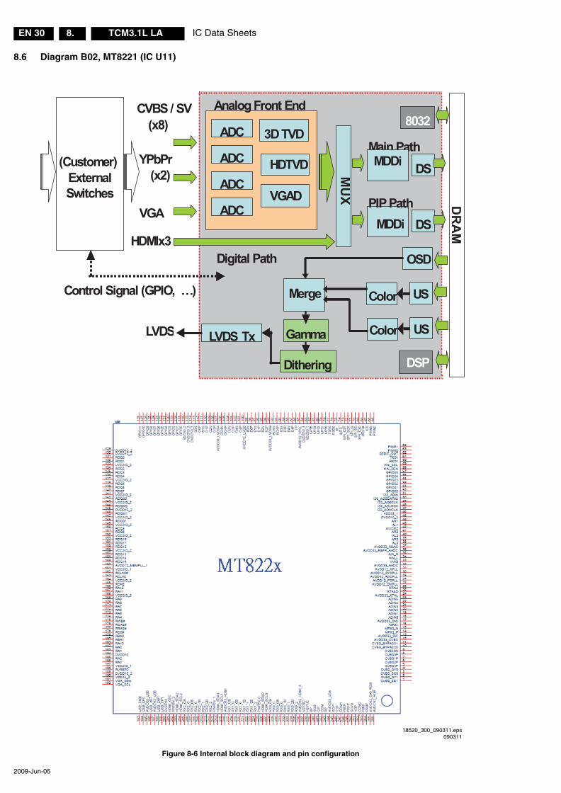
8.6 Diagram B02, MT8221 (IC U11)
Figure 8-6 Internal block diagram and pin configuration
18520_300_090311.eps090311
ADC
ADC
ADC
ADC
3D TVD
HDTVD
VGAD
DS
MDDi DS
Digital Path
Analog Front End
Main Path
PIP Path
Color
OSD
CVBS / SV
YPbPr (x2)
(Customer) ExternalSwitches
HDMIx3
VGA
(x8)
Control Signal (GPIO, …)
Gamma
Merge
Dithering
LVDS Tx
8032
DSP
MDDi
LVDS
DR
AM
MU
X
US
US
Color
IC Data Sheets EN 31TCM3.1L LA 8.
2009-Jun-05
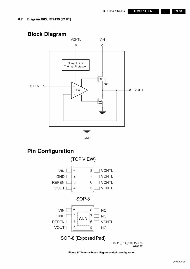
8.7 Diagram B03, RT9199 (IC U1)
Figure 8-7 Internal block diagram and pin configuration
Block Diagram
Pin Configuration
18520_314_090327.eps090327
GND
VCNTL
REFEN
Current LimitThermal Protection
VOUTEA
+
-
VIN
(TOP VIEW)
SOP-8
VINGND
REFENVOUT
VCNTL
234 5
678
VCNTL
VCNTLVCNTL
SOP-8 (Exposed Pad)
VINGND
REFENVOUT
NCNC
NCVCNTL
GND234 5
678
IC Data SheetsEN 32 TCM3.1L LA8.
2009-Jun-05
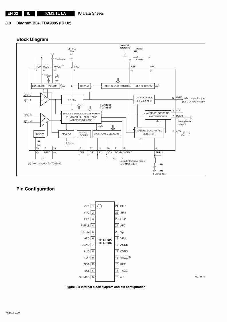
8.8 Diagram B04, TDA9885 (IC U2)
Figure 8-8 Internal block diagram and pin configuration
Block Diagram
Pin Configuration
G_16510_
TAGC
CVAGC pos
CBL
VIF-PLL
4 MHz
external
AFC
video output 2 V (p-p)[1.1 V (p-p) without trap
AUD
CAF
de-emphasisnetwork
FM-PLL filter
sound intercarrier output
CAGC
AGNDVP
VIF1
VIF-AGC RC VCO DIGITAL VCO CONTROL AFC DETECTOR
VIDEO TRAPS4.5 to 6.5 MHz
NARROW-BAND FM-PLLDETECTORI2C-BUS TRANSCEIVER
VIF-PLL
SINGLE REFERENCE QSS MIXER/INTERCARRIER MIXER AND
AM-DEMODULATOR
SIF-AGCSUPPLY
1
2
14 16 19 15 21
17
8
6
5
4127 11 101820
23
24
OUTPUTPORTS
MAD
AUDIO PROCESSINGAND SWITCHES
9
TUNER AGC
CAGC neg
3 22
crystal
and MAD select
TDA9885
n.c.
13
LLPMFDAMOISDNGDADSLCS2PO1PO
CVBS
TOP
VIF2
SIF1
SIF2 DEEM
AFD
REFVAGC VPLL
filter
TDA9886
(1)
(1) Not connected for TDA9885.
reference
or
TDA9885TDA9886
1
2
3
4
5
6
7
8
9
10
11
12
VIF1
VIF2
OP1
FMPLL
DEEM
AFD
DGND
AUD
TOP
SDA
SCL
SIOMAD
SIF2
SIF1
OP2
AFC
VP
VPLL
AGND
CVBS
VAGC(1)
REF
TAGC
n.c.
24
23
22
21
20
19
18
17
16
15
14
13
IC Data Sheets EN 33TCM3.1L LA 8.
2009-Jun-05
8.9 Diagram B07, WM8501 (IC U9)
Figure 8-9 Internal block diagram and pin configuration
Block Diagram
Pin Configuration
18520_311_090325.eps090325
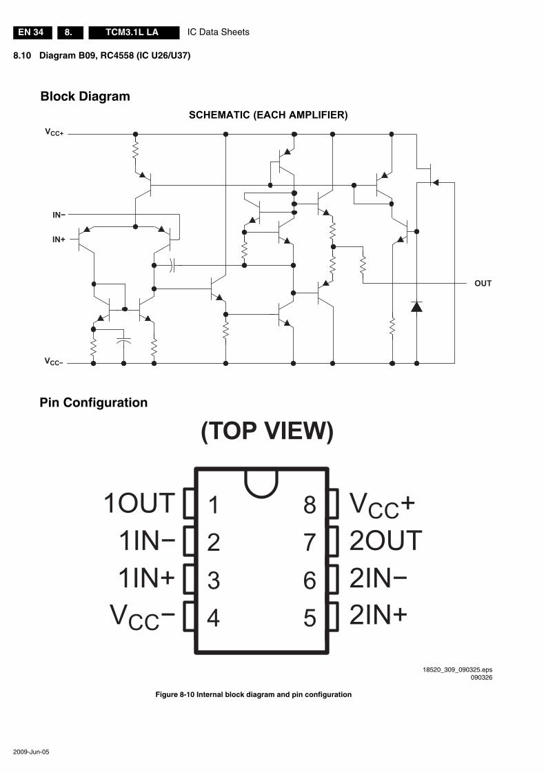
IC Data SheetsEN 34 TCM3.1L LA8.
2009-Jun-05
8.10 Diagram B09, RC4558 (IC U26/U37)
Figure 8-10 Internal block diagram and pin configuration
Block Diagram
Pin Configuration
18520_309_090325.eps090326
1234
8765
1OUT1IN−1IN+VCC−
VCC+2OUT2IN−2IN+
(TOP VIEW)
OUT
IN+
IN−
VCC−
VCC+
SCHEMATIC (EACH AMPLIFIER)
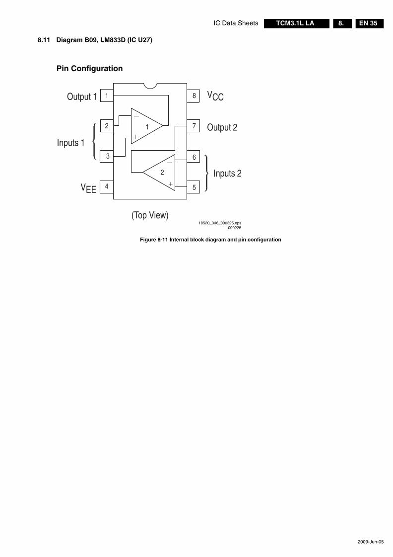
IC Data Sheets EN 35TCM3.1L LA 8.
2009-Jun-05
8.11 Diagram B09, LM833D (IC U27)
Figure 8-11 Internal block diagram and pin configuration
Pin Configuration
18520_306_090325.eps090225
2
(Top View)
1
3
4
8
7
6
5
Output 1
Inputs 1
Output 2
Inputs 2VEE
VCC
1
2
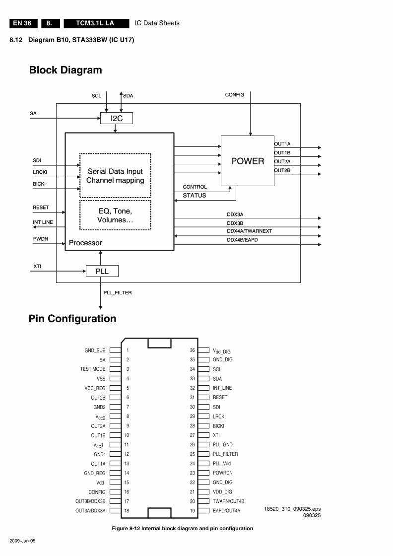
IC Data SheetsEN 36 TCM3.1L LA8.
2009-Jun-05
8.12 Diagram B10, STA333BW (IC U17)
Figure 8-12 Internal block diagram and pin configuration
Block Diagram
Pin Configuration
18520_310_090325.eps090325
Serial Data InputChannel mapping
I2C
POWER
PLL
Processor
DDX3A
DDX3B
DDX4A/TWARNEXT
DDX4B/EAPD
SCL SDA
OUT1A
OUT1B
OUT2A
OUT2BLRCKI
BICKI
RESET
SDI
XTI
PLL_FILTER
CONTROL
STATUS
INT LINE
EQ, Tone,Volumes…
SA
CONFIG
PWDN
Serial Data InputChannel mapping
I2C
POWER
PLL
Processor
DDX3A
DDX3B
DDX4A/TWARNEXT
DDX4B/EAPD
SCL SDA
OUT1A
OUT1B
OUT2A
OUT2BLRCKI
BICKI
RESET
SDI
XTI
PLL_FILTER
CONTROL
STATUS
INT LINE
EQ, Tone,Volumes…
SA
CONFIG
PWDN
GND_SUB
SA
TEST MODE
VSS
OUT1A
Vdd
GND_REG
CONFIG
B4TUO/NRAWTB3XDD/B3TUO
VDD_DIG
GND_DIG
PLL_Vdd
POWRDN
SDA
SCL
GND_DIG
Vdd_DIG
18
16
17
15
6
5
4
3
2
21
22
31
32
33
35
34
36
20
1
19 A4TUO/DPAEA3XDD/A3TUO
OUT1B
GND1
VCC1
PLL_FILTER
PLL_GND
XTI
9
8
7
28
29
30
IKCIBA2TUO
7201
VCC_REG
VCC2
GND2
LRCKI
INT_LINE
SDI
14
12
11
23
25
26
OUT2B RESET
4231
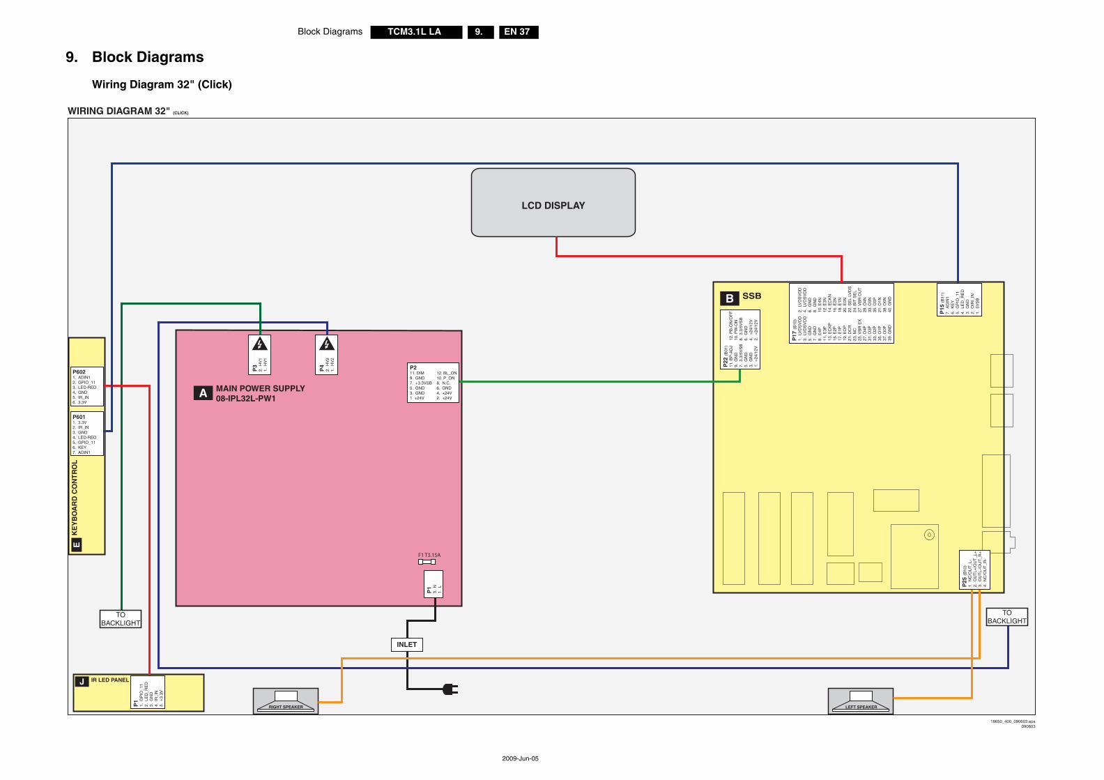
Block Diagrams EN 37TCM3.1L LA 9.
2009-Jun-05
9. Block Diagrams
Wiring Diagram 32" (Click)
P22
(B01
)11
. BP
-AD
J9.
GN
D7.
3.3
/5V
SB
5. G
ND
3. G
ND
1. +
24/1
2V
12. P
B-O
N/O
FF
10. P
W-O
N
8. 3
.3/5
VS
B6.
GN
D4.
+24
/12V
2. +
24/1
2V
P1
3. N
1. L
WIRING DIAGRAM 32" (CLICK)
SSBB
INLET
P3
2. H
V1
1. H
V1
P4
2. H
V2
1. H
V2
LCD DISPLAY
F1 T3.15A
12. BL_ON10. P_ON8. N.C.6. GND4. +24V2. +24V
P211. DIM9. GND7. +3.3VSB5. GND3. GND1 +24V
RIGHT SPEAKER LEFT SPEAKER
TOBACKLIGHT
TOBACKLIGHT
P1
1. G
PIO
_11
2. L
ED
_RE
D3.
GN
D4.
IR
_IN
5. +
3.3V
P602 1. ADIN12. GPIO_113. LED-RED4. GND5. IR_IN6. 3.3V
P601 1. 3.3V2. IR_IN3. GND4. LED-RED5. GPIO_116. KEY7. ADIN1
18650_400_090603.eps090603
IR LED PANELJ
KE
YB
OA
RD
CO
NT
RO
LE
MAIN POWER SUPPLY08-IPL32L-PW1 A
P17
(B10
)1.
LV
DS
VD
D3.
LV
DS
VD
D5.
GN
D7.
GN
D9.
E4P
11. E
3P13
. EC
KP
15. E
2P17
. E1P
19. E
OP
21. D
CR
23. N
C25
. VB
R E
X27
. O4P
31. O
3P33
. O2P
35. O
1P37
. O0P
39. G
ND
2. L
VD
SV
DD
4. L
VD
SV
DD
6. G
ND
8. G
ND
10. E
4N12
. E3N
14. E
CK
N16
. E2N
18. E
1N20
. E0N
22. S
EL
LVD
S24
. BIT
SE
L27
. VB
R O
UT
29. O
4N33
. O3N
35. O
3P21
. O1N
38. O
0N40
. GN
D
P15
(B11
)7.
AD
IN1
6. K
EY
5. G
PIO
_11
4. L
ED
_RE
D3.
GN
D2.
OIR
I_IN
1. 5
VS
B
P25
(B10
)1.
NC
/OU
T_L
-2.
OU
TL+
/OU
T_L
+3.
OU
TL-
/OU
T_R
+4.
NC
/OU
T_R
-
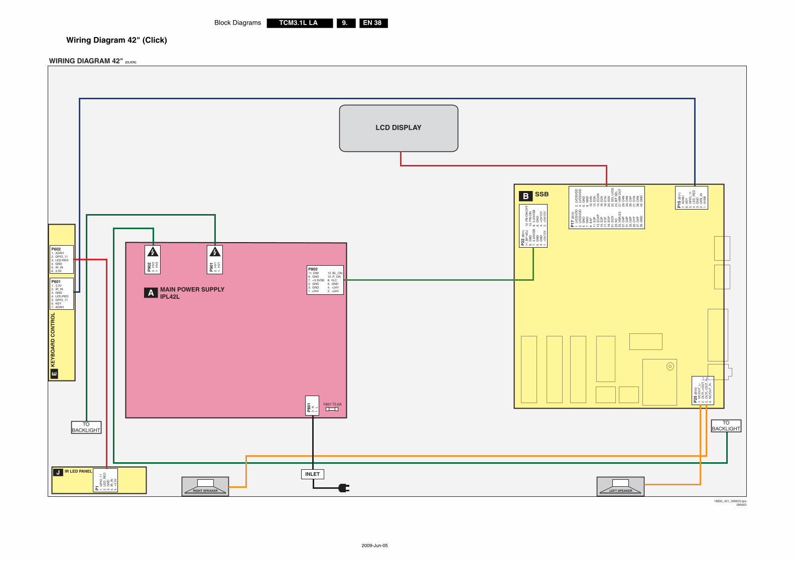
EN 38TCM3.1L LA 9.Block Diagrams
2009-Jun-05
Wiring Diagram 42" (Click)
P22
(B01
)11
. BP
-AD
J9.
GN
D7.
3.3
/5V
SB
5. G
ND
3. G
ND
1. +
24/1
2V
12. P
B-O
N/O
FF
10. P
W-O
N
8. 3
.3/5
VS
B6.
GN
D4.
+24
/12V
2. +
24/1
2V
P25
(B10
)1.
NC
/OU
T_L
-2.
OU
TL+
/OU
T_L
+3.
OU
TL-
/OU
T_R
+4.
NC
/OU
T_R
-
WIRING DIAGRAM 42" (CLICK)
SSBB
INLET
LCD DISPLAY
F801 T5.0A
12. BL_ON10. P_ON8. N.C.6. GND4. +24V2. +24V
P80211. DIM9. GND7. +3.3VSB5. GND3. GND1 +24V
RIGHT SPEAKER LEFT SPEAKER
TOBACKLIGHT
TOBACKLIGHT
P1
1. G
PIO
_11
2. L
ED
_RE
D3.
GN
D4.
IR
_IN
5. +
3.3V
P602 1. ADIN12. GPIO_113. LED-RED4. GND5. IR_IN6. 3.3V
P601 1. 3.3V2. IR_IN3. GND4. LED-RED5. GPIO_116. KEY7. ADIN1
18650_401_090603.eps090603
IR LED PANELJ
KE
YB
OA
RD
CO
NT
RO
LE
MAIN POWER SUPPLYIPL42L A
P90
22.
HV
21.
HV
2
P90
12.
HV
11.
HV
1
P80
13.
N1.
L
P17
(B10
)1.
LV
DS
VD
D3.
LV
DS
VD
D5.
GN
D7.
GN
D9.
E4P
11. E
3P13
. EC
KP
15. E
2P17
. E1P
19. E
OP
21. D
CR
23. N
C25
. VB
R E
X27
. O4P
31. O
3P33
. O2P
35. O
1P37
. O0P
39. G
ND
2. L
VD
SV
DD
4. L
VD
SV
DD
6. G
ND
8. G
ND
10. E
4N12
. E3N
14. E
CK
N16
. E2N
18. E
1N20
. E0N
22. S
EL
LVD
S24
. BIT
SE
L27
. VB
R O
UT
29. O
4N33
. O3N
35. O
3P21
. O1N
38. O
0N40
. GN
D
P15
(B11
)7.
AD
IN1
6. K
EY
5. G
PIO
_11
4. L
ED
_RE
D3.
GN
D2.
OIR
I_IN
1. 5
VS
B
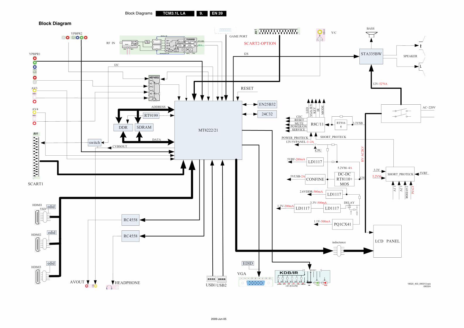
Block Diagrams EN 39TCM3.1L LA 9.
2009-Jun-05
Block Diagram
MT8222/21
STA335BW
RC4558
DDR
EN25B32
12V-52"6A
SDRAM
ADDRESS
DATA
I2S
inductance
edid
edid
edid
YPBPR1
YPBPR2
HDMI1
HDMI2
HDMI3
USB1USB2
RC4558
ESD
I2C
EDID
GAME PORT
CVBSOUT
24C32
RESET
RT9199
SCART2-OPTION
Y/CBASS
SPEAKER
12V/5VPANEL-1~2Aswitch
HEADPHONEAVOUT
RT9166
AV3
CPU
AC~220VAV4
VGA
RF IN
SCART1
DC-DCRT8110+
MOS
5.2VM- 4A
LD11175VRF-200mA
CONFINE5VUSB-2A
LD1117
LD1117
PQ1CX411.1V-500mA
LD11171.2V-200mA3.3V-500mA
2.6VDDR-500mA
DELAY
SHORT_PROTECK 5VRF
12VM
2.6VD
DR
1.2V
1.1V
3.3V
5.2VM
LCD PANEL
12V
R8C/11
CECRESETMUTE
POWER/ONSERVICE
LED
VG
A H
/VK
EY IRM
OD
E
SHORT_PROTECKPOWER_PROTECK
HV
AC
2KV
3.3VSB
18520_403_090313.eps090324
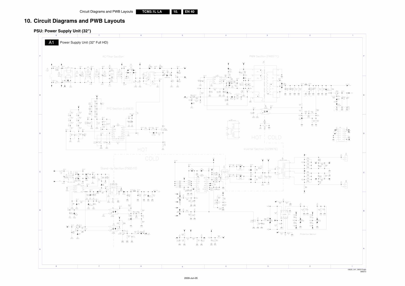
EN 40TCM3.1L LA 10.Circuit Diagrams and PWB Layouts
2009-Jun-05
10. Circuit Diagrams and PWB Layouts
PSU: Power Supply Unit (32")
A
3 2 1
F
E
D
C
B
8 7 6 5
5
4 3 2 1
F
E
D
C
B
A
4678
A1 Power Supply Unit (32" Full HD)
18520_541_090313.eps090313
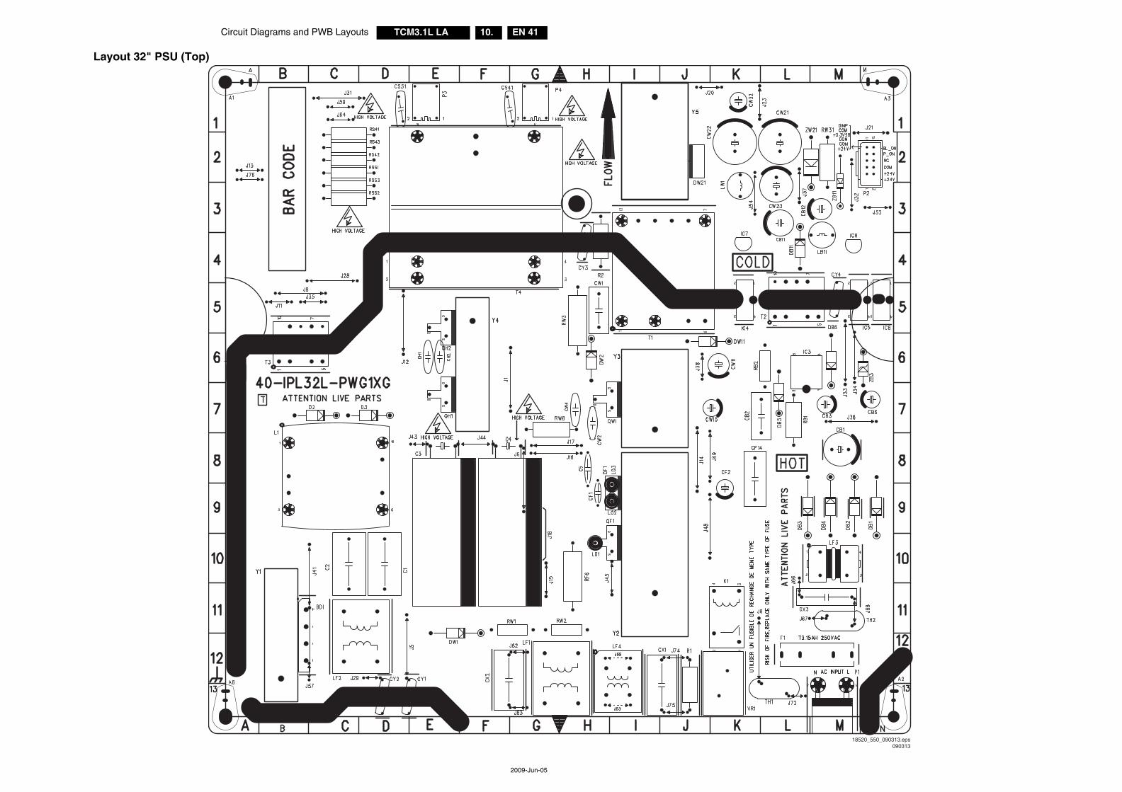
Circuit Diagrams and PWB Layouts EN 41TCM3.1L LA 10.
2009-Jun-05
Layout 32" PSU (Top)
18520_550_090313.eps090313
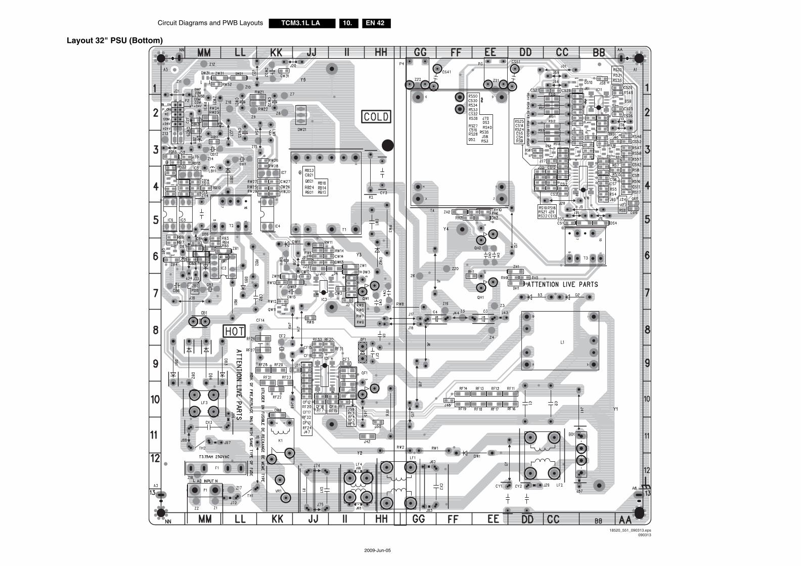
EN 42TCM3.1L LA 10.Circuit Diagrams and PWB Layouts
2009-Jun-05
Layout 32" PSU (Bottom)
18520_551_090313.eps090313
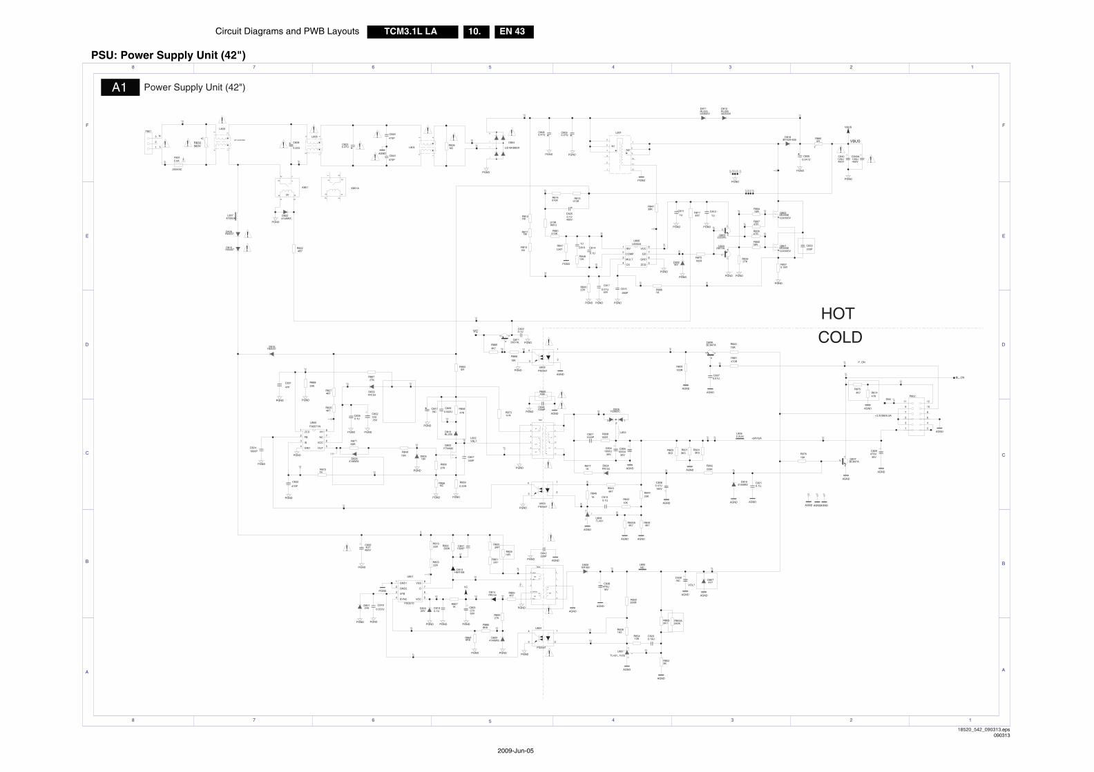
Circuit Diagrams and PWB Layouts EN 43TCM3.1L LA 10.
2009-Jun-05
PSU: Power Supply Unit (42")
A
3 2 1
F
E
D
C
B
8 7 6 5
5
4 3 2 1
F
E
D
C
B
A
4678
A1 Power Supply Unit (42")
I
I
I
I
I
I
I
I
I II
I II
I
I
I
I
I
I I
I
I
I
I
I
II
I
I
I
I
I
I
I
I
I
I
I
I
I
II
I
I
I
I
I
I
II
II
I
I
I
I
I
I
I
I
I
I
I
I I
I
!
!
!
!
!
!
PGND
PGND
NP1
NP2
ND
NS'
NS
!
+~
~-
VAL?
!
!
!
!
!
V !
OUT
VCC
NC
VH
GND
IS
FB
ZCD
!
VCC
D
VSS
SYNC
VFB
GND2
GND1
N2
N1
PGND
!!
2
34
1 2
3 4
1
VOL?
!
!
!!
!!!
T
!
!!
I
I
I
VC+
DRAIN
16V
GND
NP
ND
NS
II
I
I
I
I
I
I
I
INV
ZCD
MULT GND
CS
GDCOMP
VCC
I
N
L
3V
HOT
COLD
C8260.022U
Z130
RL255D810
D811RL2553A/600V
47K
R858
1
5
3 6
4
72
8
U806L6562A
Z12268RR871
Z67
Z109
4K7R875
Z117
R83510M
Z5
VBUS
Z41
Z7
Z22 Z21
10
3
6
7
8
9
1
2
4
5
T802
PGND
Z42
Z32
R84139K
R8861K
R80322K
Z1
R853A240K
4V7D807
D8015V6
R87447K
1
10
11 12
2
3 4
5 6
7 8
9
P802
27KR887
FR104D829
220PC833
C807330P
R80910R
R8590.33R
5RR860
C839NC
NCL805
C815
680P
R80747R
47RR806
0.1UC813
12
3
D806YG902C
C842220P
5K1R853
C8200.15U
R8381K2
470RR881
1 2
3 4
K801A
C812
1U
R80410R
10RR805
R829100R
27KR866
10RR849
R88839K47P
C801
4R7R865
R8701K
6K8R864
R8806K8
4K7R885
10K
R868
0.1UC835
1000PC824
470P
C832
0.01UC837
R84420K
R8464K74K7
R846A
0.1UC821
R8771K
R8671K
1
4 3
2
K801
F8015.0A
250VAC
20VD803
4148WSD820
PGND
10KR842
R8434K7
D814FR104
AGND
47RR873
3KR852
C811
1U
18VD802
D80518V
VBUS
12
4
1
8
10
76
3
2
5
9
11
L801
D8151N4007 4R7
R822
PGND
C80322U50V
PGND PGND
25V10UC802
PGND
4148WSD828
PGND
C8360.47U160V
C8220.1U
C8080.47U
10KR876
R802220K
35V1000UC805
5
7
8
4
3
2
1
6
U801
FSQ510
C8271000P
D824FR104
L803
C847NC
C8064U7
450V
PGND
PGND
R836NC
D818BYV29-600
L8074700UH
1
34
2
L809
LIF-JLB1359
4148WSD822
PGND
AGND
5
6
7
8
4
3
2
1
U805FA5571N
R82075R
4148WSD819
R85410K
1
23
U807
TL431_1V25
43
2
1
L804
AGND
R830560V
1N4007D816
43
2
1
L808
L8062.2UH
1
23
4U804
PS2561
4
32
1
U802PS2561
C8441000P
PGNDAGND
AGND
PGND
PGND
AGND
AGND
AGND
AGND
AGND
AGND
AGNDPGND
PGND
AGNDAGND
AGNDAGND
PGND
PGND
PGND
PGND
PGNDPGND
PGND
PGNDPGND
PGND
PGND
PGNDPGND
PGND
R808100R
NCR856
D813HER108
0.047UC830
C8230.47U
C8090.47U
C8411500P
B
CE
BC847AQ808
1
2
3
TL431U808
B
C
E
BC847AQ807
R8630R
L802
Q803P7NK80
1KR845
200RR850
R862390K
R83927K
B
C
EQ8052222AL
R861470K
1
2
3
P801
R81922K
R8264K7
R8274K7
B
E C
Q8112907AL
D809SR160
D804
US10KB80R
510KR815
22KR840
C814
0.1U
12KR848
1U
C81612K7R847
C817
0.01U50V
R872100R
R8174R7
B
E
C
Q8092907AL
510KR813
400V0.1UC825
R814510K
R85527K
0.022U
C818
0.1UC819
3K3R823 R821
3K3
1MR810
1MR811
1MR812
D812RL2553A/600V
C840120U450V
12
2
3
5
7
10
6
4
1
9
11
8
T801
C840A120U450V
1
23
4
PS2561U803
C828
0.22U
470P
C843
C845
470P
2R7R825
D8081N4007
C829470U35V
C8041000U
35V
R8370.15R
12A/500VSK3568Q802
Q801SK356812A/500V
C838470U16V
3K3R824
R8012R7
VC
PGND PGND
PGND
PGND
PGND
PGND
PGND
PGND
AGND
AGND
AGND
AGND
AGND
AGND
PGND
PGND
PGND
PGND
PGND
AGND
PGND
VC
AGND
Z25
Z105Z106
Z107
Z108
Z110
Z111
Z112
Z113
Z114
Z115
Z116
Z118
Z119
Z120 Z121
Z123 Z124
Z125
Z26
Z27
Z28
Z29
Z30
Z31 Z33
Z34
Z35
Z36
Z37
Z38
Z39
Z40
Z43
Z44
Z45
Z46
Z47
Z48
Z49 Z50
Z51
Z52
Z53
Z126
Z127
AGNDAGND
Z19Z20
P_ONZ18
BL_ONZ16
DIM Z17
Z14+24V/2A
+3.3VSB/0.2A
Z15
Z8 Z10Z9
Z11 Z12Z6
PGND
Z2
Z128
Z4
Z3
AGND
Z13
Z73
Z129
Z131
18520_542_090313.eps090313
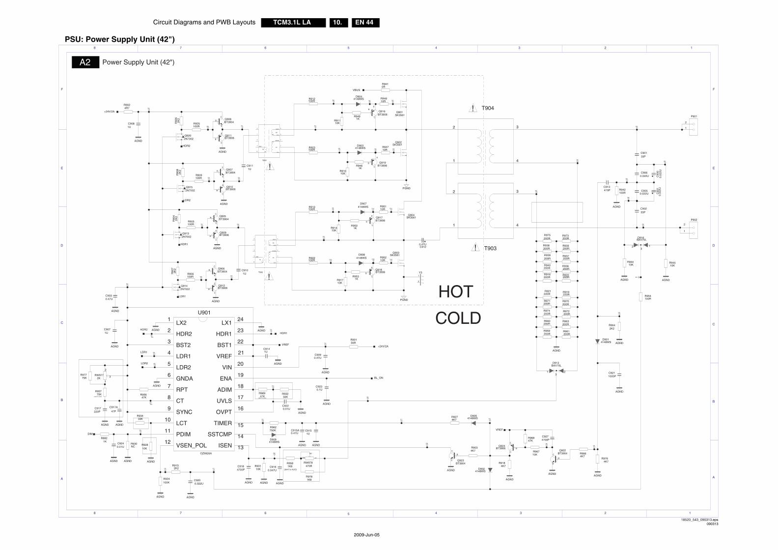
EN 44TCM3.1L LA 10.Circuit Diagrams and PWB Layouts
2009-Jun-05
PSU: Power Supply Unit (42")
A
3 2 1
F
E
D
C
B
8 7 6 5
5
4 3 2 1
F
E
D
C
B
A
4678
A2 Power Supply Unit (42")
I
I
III
II
I
I
III
I II
I
I
I
I
I
I
I
I
I
II
III
I
I
I
II
I
I
I
I
I
I
I
II
I
I
I
I
!
!
ADIM
BST1BST2
CT
ENAGNDA
HDR1HDR2
ISEN
LCT
LDR1
LDR2
LX1LX2
OVPT
PDIM
RPT
SSTCMP
SYNC
TIMER
UVLS
VIN
VREF
VSEN_POL
VCC
GND1
DRAIN
VC+
GND
ND
NP
NS
VCC
GND1
DRAIN
VC+
GND
ND
NP
NS
!
!
I
I
I
I
HOT
COLD
(39K For AUO)
(2k4 For AUO)
(56K For AUO)
R9781K8
R9581K8
R95775K
R97775K
2
1
Y3
1
3
2
RW9772K
10KR928
33KR934
NCR930
C93
10.
022U
C93
00.
022U
Z83
2
3
1470R
RW978
R96947K
C917A
47P
AGNDAGND
220PC917
AGND
321
BAV70LD913
AGND
Z84
R94810R
4148WSD903
D9044148WS
10KR967
Z68
Z64
1UC911
C9101UR906
100R
100RR905
100RR909
R925100R
BL_ON
56RR901
+24V/2A
R924100K
56KR932
C9151U
C915A0.47U
0.022UC906
B
C
E Q923BT3904
C9050.022U
1KR953
AGND
C9071U
AGND
C9141U
4148WSD909
C9200.022U
2K2R915
0.047UC916
C9274700P
R96847K
R9274K7
R9410R
R912100R
10KR911
R9491K
10RR947
1KR946
R91010K
100RR923
R913100R
10KR914
R9501K
10RR951
100RR922
R91710K
R95210R
C9220.01U
C9230.1U
0.47UC903
0.01UC924
4K7R976
C90233P
470PC913
C9211000P
2K2R964
R94410K 10K
R945
100RR954
R93110K
C9184700P
750KR962
4148WSD902
VREF
D9054148WS
R961200R
200RR963
200RR972
R970200R
220RR919
200RR959
R960200R
R974200R
200RR971
R921220R
R920200R200R
R916
R936200R200R
R940
R937200R200R
R939
200RR935R938
200R
R973200R200R
R975
R9024R7
C9090.47U
R9664K7
4K7R903
R9184K7
SK3561Q902
D9014148WS
R942100R
AGND
R8821K
2
41
3
T904
2
41
3
T903
B
C
E
Q906BT3904
10
2
6
7
8
4
5
3
1
9
T902
9
1
3
5
4
8
7
6
2
10
T901
AGND
AGND
B
C
E
Q924BT3906
E
C
B
BT3904Q922
123
D916BAV70L
C90133P
AGND
AGND
12
11
23
4
3
2
1
10
9
8
7
6
5
13
14
15
17
18
19
20
21
16
22
24U901
OZ9926A
47KR956
PGND
AGND
+24V/2A
DIM
1
2
P902
AGND
AGND
AGND AGND
AGND
E
C
B BT3906Q909
AGND
E
C
BBT3904Q907
AGNDAGND
4148WSD908
D9074148WS
AGND
AGND
AGND
AGND
AGND
AGND
AGND
AGND
PGND
R90
82K
2
R90
42K
2R
907
2K2
R92
62K
2
C9120.47U
Q903SK3561
SK3561Q904
Q901SK3561
2N7002Q913
C9081U
Q9142N7002
E
C
B
BT3906Q916
B
C
E
Q919BT3906
E
C
B BT3906Q917
B
C
EQ918BT3906
E
C
B BT3906Q910
LDR1
HDR1
LDR2
HDR2
E
C
BBT3904Q905
B
C
EQ911BT3906
B
C
E
Q908BT3904
B
C
EQ912BT3906
Q9202N7002
2
1
P901
2N7002Q915
VBUS
AGND
AGNDAGND
AGNDAGND
AGND
AGND
AGND
Z54
Z55
Z56
Z57
Z58Z59
Z60
Z61
Z62
Z63
HDR2
Z65LDR1
Z66LDR2
Z69
Z70 Z71
Z72
HDR1
Z74
Z75
Z76 Z77 Z78
Z79 Z80
Z81
Z82
Z85
Z86
Z87
Z88
Z89
Z90
Z91
Z92 Z93Z94
Z95 Z96 Z97
Z98
Z99
Z100 Z101
Z102 Z103 Z104
Z24
Z23
VREF
18520_543_090313.eps090313
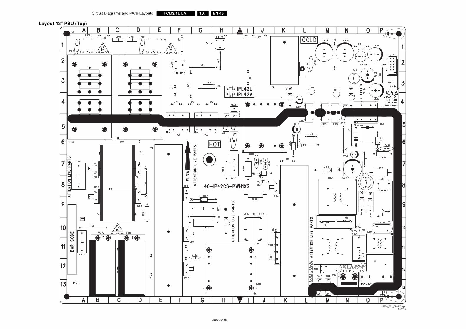
Circuit Diagrams and PWB Layouts EN 45TCM3.1L LA 10.
2009-Jun-05
Layout 42" PSU (Top)
15820_552_090313.eps090313
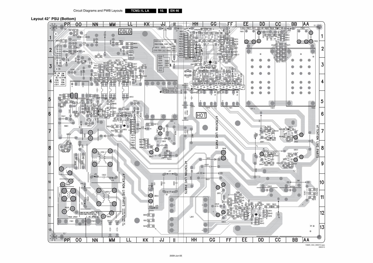
EN 46TCM3.1L LA 10.Circuit Diagrams and PWB Layouts
2009-Jun-05
Layout 42" PSU (Bottom)
15820_553_090313.eps090313
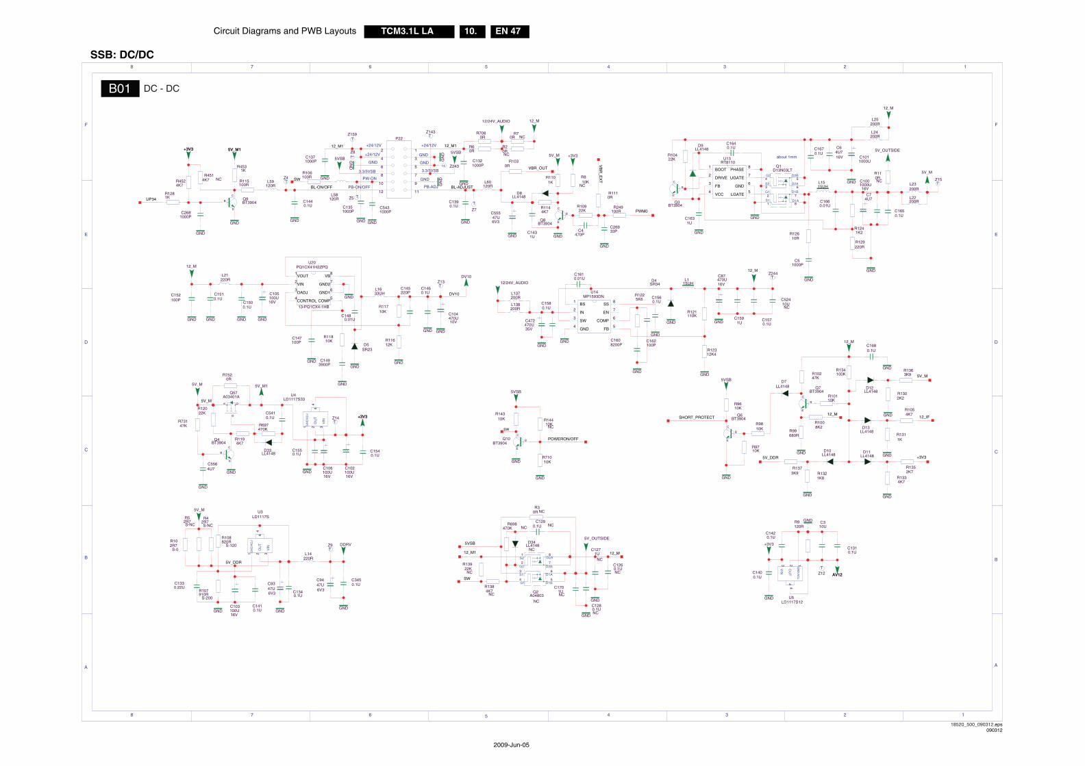
Circuit Diagrams and PWB Layouts EN 47TCM3.1L LA 10.
2009-Jun-05
SSB: DC/DC
GND
GND
GND
GND
GND
T
GND
GND
GND
GND
GND
GND
T
GND
GND
GN
D
GN
D
GNDGND
T
GND
T
GND
GND
GND
GND
GND
GND
GND GND GND GND
T
GND
GND
GND
GND
GND
GND
T
GN
D/A
DJ
OU
T
VIN
4
GND
D1B
D1A
G2
G1
S2
D2B
D2A
S1
GND
T
T
GND
GND
GND
T
GND
GND
T
GNDT
GND
T
GND
T
A
3 2 1
F
E
D
C
B
8 7 6 5
5
4 3 2 1
F
E
D
C
B
A
4678
GND
GND
GND
GND
GND
GN
D
GND
GND
GND
GND
GND
GND
GN
D/A
DJ
OU
T
VIN
4
COMP
GND1
GND2
VB
CONTROL
OADJ
VIN
VOUT
BS
IN
SW COMP
FB
SS
GND
EN
GN
D/A
DJ
OU
T
VIN
4
BOOT
DRIVE
FB GND
LGATE
PHASE
VCC
UGATE
D2B
D2A
G1
G2
S1
D1B
D1A
S2
PB-ADJ
GND
GND
PW-ON
PB-ON/OFF
about 1mmGND
GND
+24/12V+24/12V
+24/12V
3.3/5VSB3.3/5VSB
10KR143
10V470UC104
1UC163
R14410K
NC
0RR752
22KR120
47KR731
R20RNC
R70R NC
7
8
4
2
3
5
6
1
A04803Q2
NC
C1701UNC
0.1UC128
NC
0.1UC126
NC
1UC127
NC
1
2
3 6
5
8
4
7
RT8110U13
R60R
R7080R
910RR107
S-200
1 2 3
4
LD1117SU3
2R7R4
S-NC2R7R5
S-NC
2R7R10
S-0
R110RNC
D34LL4148
NC
22KR139
NC
R698470K NC
C1290.1U NC
R30R NC
1
2
3 6
5
8
4
7
U14MP1593DN
C55547U6V3
4K7R114
R1030R
LL4148D8
1UC143
R1110R
470PC4
22KR109
B
C
EBT3904Q8
R249100R
1KR110
10KR8
NC
1KR453
4K7R451
NC
4K7R452
4K7R138
NC
16V100UC106
16V100UC103
16V100UC102
220RL21
220RL14
5
6
7
8
4
3
2
1
PQ1CX41H2ZPQU20
13-PQ1CX4-1HB10UC524
NC
10RR126
L1633UH
L115UH
15UHL15
1 2 3
4
LD1117S33U4
100RR106
5V_M1
5V_M15V_M1
DV10
DV10
L24200R
200RL25
12
4
6
8
12
10
3
5
7
9
11
P22
C26933P
PWM0
120RL60
1KR128
UP34
SW
POWERON/OFF
16V1000UC100
16V1000UC101
R121110K
4U7C7
820RR108
S-120
L138200R
200RL137
1K2R124
5VSB
12_M
R12312K4
B
C
E
BT3904Q4
4U7C556
12_M
12_M112_M1
C5410.1UG
DS
A03401AQ57
1UC159
+3V3+3V3
4U7C6
B
C
E
BT3904Q3
SHORT_PROTECT
100PC162
8200PC160
0.1UC156
5VSB
5VSB
220RR129
0.1UC157C472
470U35V
16V470UC87
SR34D4
5K6R122
0.01UC161
0.1UC158
10KR710
12KR116
10KR117
100PC147
0.01UC148
0.1UC167
0.1UC165
12/24V_AUDIO
AV12AV12
L58120R
4K7R119
1000PC543
SW
5VSB
12_M
Z244
5V_DDR
DDRVZ9
0.1UC155
VBR_OUT
B
C
E
Q9BT3904
100RR115
Z4
12/24V_AUDIO
B
C
E
BT3904Q10
0.1UC140
BL-ADJUST
VB
R_E
XT
B
C
E
Q6BT3904
LL4148D12
R1321K8
R1373K9
5V_DDR
12_IF
R1311K
R1054K7
3K9R136
+3V35V_M
12_M
1000PC132
Z243
Z8
16V100UC105
12_M
0.1UC139
Z143
Z71000PC135
12_M1
100PC152
5V_OUTSIDE
R697470K
D33LL4148
7
8
4
2
3
5
6
1
D13N03LTQ1
6V347UC93
5VSB
123
4
LD1117S12U5
Z15
LL4148D13
R1352K7
R134100K
4K7R133
D11LL4148
D10LL4148
R1302K2
6V347UC94
200RL23
L22200R
0.1UC164
1000PC5
LL4148D9
0.1UC154
Z14
0.1UC151
0.1UC150
10KR118
3900PC149
0.1UC146
Z13
SR23D5
220PC145
Z12
0.1UC142
10UC3
0.1UC141
L59120R
1000PC137
0.1UC345
Z5
5V_M
0.1UC134
0.22UC133
120RR9
22KR104
R10247K
B
C
E
Q7BT3904
D7LL4148
10KR101
8K2R100
680RR99
R9810K
R9710K
R9610K
0.1UC131
5V_M
+3V3+3V3 5V_OUTSIDE
5V_M
+3V3
+3V3
12_M
SW
5V_M
Z159
12_M
0.1UC168
0.1UC144
BL-ON/OFF
C2681000P
C1660.01U
5V_M
B01 DC - DC
18520_500_090312.eps090312
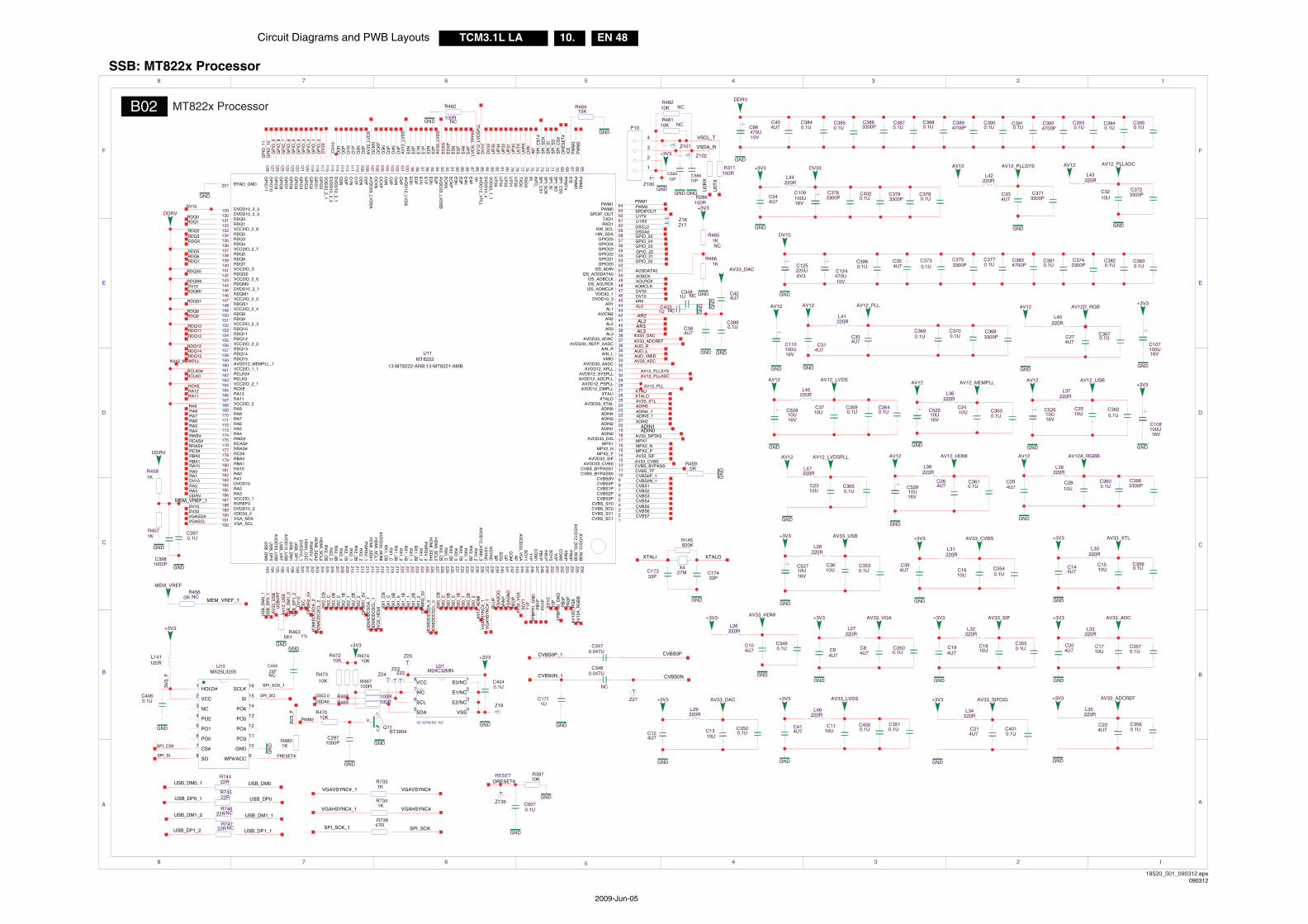
EN 48TCM3.1L LA 10.Circuit Diagrams and PWB Layouts
2009-Jun-05
SSB: MT822x Processor
GND
GND
T
GND
GND
T
GNDG
ND
GND
GNDGND
GND GND GND
GND
GNDGND
GND
GND
GND
GND
GND
GND
GND
GND
GN
D
GND
GND
GND
GND
GND
GND
GND GND GNDGND
GND
TTT
GNDGND
GND
A
3 2 1
F
E
D
C
B
8 7 6 5
5
4 3 2 1
F
E
D
C
B
A
4678
GND
GN
D
GND GND
T
SDA
SCL
WC
VCC
VSS
E2/NC
E1/NC
E0/NC
GND
GND
GND
GND
GNDGNDGND
T
T
T
T
T
GND
GN
D
CVBS_SC1CVBS_SY1CVBS_SC0CVBS_SY0
CVBS3PCVBS2PCVBS1PCVBS0PCVBS0N
CVBS_BYPASS0CVBS_BYPASS1
AVDD33_CVBSAVDD33_SIF
MPX2_PMPX2_N
MPX1AVDD33_DIG
ADIN0ADIN1ADIN2ADIN3ADIN4ADIN5
AVDD33_XTALXTALOXTALI
AVDD12_DMPLLAVDD12_PSPLL
AVDD12_ADCPLLAVDD12_SYSPLL
AVDD12_APLLAVDD33_AADC
VMIDAIN_LAIN_R
AVDD33_REFP_AADCAVDD33_ADAC
AL3AR3AL2AR2
AVICM2AL1AR1
DVDD10_3VDD33_1
I2S_AOMCLKI2S_AOLRCKI2S_AOBCLK
I2S_AOSDATA0I2S_ADIN
GPIO20GPIO21GPIO22GPIO23GPIO24GPIO25
HW_SDAHW_SCL
RXD1TXD1
SPDIF_OUTPWM0PWM1
VGA_SCLVGA_SDAVDD33_2DVDD10_2RVREF0VCC2IO_1RA3RA2DVDD10RA1RA0RA10RBA1RBA0RCS#RRAS#RCAS#RWE#RA4RA5RA6RA7RA8RA9VCC2IO_2RA11RA12RCKEVCC2IO_2_1RCLK0RCLK0#VCC2IO_1_1AVDD12_MEMPLL_1RDQ15RDQ14RDQ13VCC2IO_2_2RDQ12RDQ11RDQ10VCC2IO_2_3RDQ9RDQ8VCC2IO_2_4RDQS1VCC2IO_2_5RDQM1DVDD10_2_1RDQM0VCC2IO_2_6RDQS0VCC2IO_3RDQ7RDQ6RDQ5VCC2IO_2_7RDQ4RDQ3RDQ2VCC2IO_2_8RDQ1RDQ0DVDD10_2_2DVDD10_2_3
AV
DD
12_RG
BA
VD
D12_D
IG_R
GB
PR
0PP
B0P
CO
M0
Y0P
SO
Y0
PR
1PP
B1P
CO
M1
Y1P
SO
Y1
AV
DD
33_VG
AR
PC
OM
GP
SO
GBP
HS
YN
CV
SY
NC
AV
DD
12_HD
MI_3
RX
0_2
RX
0_1R
X0_2B
RX
0_1BR
X0_0
RX
0_CR
X0_0B
RX
0_CB
HD
MI_S
CL0
HD
MI_S
DA
0P
WR
5V_0
RX
1_2
RX
1_1R
X1_2B
RX
1_1BR
X1_0
RX
1_CR
X1_0B
RX
1_CB
AV
DD
33_HD
MI
HD
MI_S
CL1
HD
MI_S
DA
1P
WR
5V_1
RX
2_2
RX
2_1R
X2_2B
RX
2_1BR
X2_0
RX
2_CR
X2_0B
RX
2_CB
HD
MI_S
CL2
HD
MI_S
DA
2P
WR
5V_2
HD
MI_C
EC
DV
DD
10_1U
SB
_DP
1U
SB
_DM
1A
VD
D12_U
SB
US
B_V
RT
AV
DD
33_US
BU
SB
_DP
0U
SB
_DM
0
PW
M2
PW
M3
ICE
PR
ST
#S
PI_C
S0
SP
I_SO
SP
I_SI
SP
I_SC
KS
PI_C
S1
INT
0_IR
_R
XD
0T
XD
0U
P30
UP
31U
P33
UP
34U
P35
VD
D33_1_1
DV
DD
10_4A
VD
D12_V
PLL
TP
E4P
E4N
E3P
E3N
EC
KP
EC
KN
AV
DD
33_LVD
SB
E2P
E2N
E1P
E1N
E0P
E0N
AV
DD
12_LVD
SO
4PO
4NO
3PO
3NO
CK
PO
CK
NA
VD
D33_LV
DS
AO
2PO
2NO
1PO
1NO
0PO
0ND
VD
D10_3_1
DV
DD
10_3_2V
DD
33_2_1G
PIO
0G
PIO
1G
PIO
2G
PIO
3G
PIO
4G
PIO
5G
PIO
6G
PIO
7G
PIO
8G
PIO
9G
PIO
10G
PIO
11
EPAD_GND
PO2
VCC
NC
CS#
PO1
PO0
WP#/ACC
PO3
GND
PO4
PO6
PO5
SO
HOLD# SCLK
SI
T
GND
RESET
IIC ADRESS "A0"
C124470U10V
C88470U10V
XTALI XTALO
C125220U6V3
Z102
R286100R
R311100RC566
10P
C56510P
R47210K
R145820K
C17433P
C17333P
X427M
C110100U16V
C109100U16V
16V100UC108
16V100UC107
4
2
3
7
5
6
9
11
10
12
14
13
8
1 16
15
U10MX25L3205
R4635K1 1%
L141120R
12345678910111213141516171819202122232425262728293031323334353637383940414243444546474849505152535455565758596061626364
192191190189188187186185184183182181180179178177176175174173172171170169168167166165164163162161160159158157156155154153152151150149148147146145144143142141140139138137136135134133132131130129
256255254253252251250249248247246245244243242241240239238237236235
233234
232231
229230
228227226225224
222223
221220
218219
217216215214213212
210211
209208
206207
205204203202201200199198197196195194193
6566676869707172737475767778798081828384858687888990919293949596979899100101102103104105106107108109110111112113114115116117118119120121122123124125126127128
257
U11MT8222
13-MT8222-ARB;13-MT8221-AMB
22RR747
NC
22RR746
NC
USB_DP1_1
1UC348
NC
C4031U NC
USB_DP1_2
USB_DM1_2
USB_DP0_1
USB_DM0_1 USB_DM0
USB_DP0
USB_DM1_1
22RR745
22RR744
1KR733
C40533PNC
PWM2
3V3_
F
+3V3
Z27
CVBS0N
Z136
R39710K
1UC171
C3460.047U
NC
C3470.047U
CVBS0P_1 CVBS0P
VSDA_R
SPI_SCK_1
SPI_SCK_1
3V3_
F
L40220R
C3710U
SPI_SO
47RR739
SPI_SCK
1KR734
R47010K
VGAHSYNC#
VGAVSYNC#VGAVSYNC#_1
VGAHSYNC#_1
1KR480
Z101
Z100
Z16
C3981000P
U0R
X
+3V3
R4651KNC
R4661K
U0T
X
R48110K NC
R48210K NC
+3V3
C2971000P
C3970.1U
R4571K
220RL26
220RL29
R4560R NC
5
6
7
8
4
3
2
1
U21M24C32MN
Z25
C3990.1U
0.1UC358
C5070.1U
C3723300P
R47310K
R46410K
C4060.1U
+3V3
R47410K
+3V3
C4040.1U
B
C
EQ11
BT3904
R469 100RR468 100R
R467100R
Z24Z23
Z22
AV33_DAC
DDRVR462
100RNC
C4020.1U
MEM_VREF
0.1UC4010.1U
C400
C424U7
R4590R
DDRV
R4581K
C3960.1U
C3950.1U
C3940.1U
C3930.1U
C3924700P
C3910.1U
C3900.1U
C3894700P
C3880.1U
C3870.1U
C3863300P
C3850.1U
C3840.1U
+3V3
L47220R
AV33_LVDS
AV33_VGA
4U7C41
C404U7
4U7C39
DDRV
C384U7
AV33_DAC
220RL46
AV12+3V3
C3830.1U
C3820.1U
C3810.1U
AV33_ADCREF
AV33_ADC
AV33_XTL+3V3
AV33_SIFDIG+3V3
AV33_SIF
+3V3+3V3
AV33_HDMI
AV33_USB AV33_CVBS
AV12A_RGBB
AV12 AV12_USB+3V3
AV12_HDMI
AV12 AV12_MEMPLL
AV12_PLLSYS AV12_PLLADC
AV12 AV12D_RGB
AV12
AV12_LVDSPLL
AV12
AV12_LVDS
AV12_PLLAV12
+3V3
C52910U16V
DV33
DV10
L45220R
10UC36
C52810U16V
16V10UC527
L44220R
C354U7
C3804700P
C3793300P
C3780.1U
C3770.1U
C3763300P
C3753300P
C344U7
C3743300P
C3730.1U
C334U7
C3210U
L43220R
C314U7
L42220R
L41220R
C3713300P
C3700.1U
C3690.1UC30
4U7
C3683300P
C294U7
C2810U
C3670.1UC27
4U7
C3663300P
C264U7
C52610U16V
L39220R
L38220R
C2510U
C2410U
L37220R
L36220R
C2310U
C3650.1U
C3640.1U C363
0.1UC3620.1U
C3610.1U
C3600.1U
C3590.1U
4U7C22
4U7C21
4U7C20
4U7C19
10UC18
10UC17
10UC16 10U
C154U7C14
0.1UC357
0.1UC356
0.1UC355
0.1UC354
220RL35
220RL34
220RL33
220RL32
220RL31
220RL30
10UC13
4U7C12
0.1UC353
0.1UC352
220RL28
10UC11
0.1UC351
4U7C10
4U7C9
4U7C8
0.1UC3500.1U
C349
220RL27
+3V3
+3V3+3V3
AV12
AV12
AV12
+3V3
AV12
+3V3 +3V3
Z18
Z17
FRESET#SPI_SI
SPI_CS#
OSDA0OSCL0
MEM_VREF_1
16V10UC525
ORESET#
1
2
3
4
P10
VSCL_T
CVBS0N_1
GP
IO_1
1G
PIO
_10
GP
IO_9
GP
IO_8
GP
IO_7
GP
IO_6
GP
IO_5
GP
IO_4
GP
IO_3
GP
IO_2
GP
IO_1
GP
IO_0
DV
33
DV
10O
0NO
0PO
1NO
1PO
2NO
2PA
V33
_LV
DS
OC
KN
OC
KP
O3N
O3P
O4N
O4P
AV
12_L
VD
SE
0NE
0PE
1NE
1PE
2NE
2PA
V33
_LV
DS
EC
KN
EC
KP
E3N
E3P
E4N
E4P
AV
12_L
VD
SP
LLD
V10
DV
33U
P35
UP
34U
P33
UP
31U
P30
U0T
XU
0RX
OIR
IIN
TS
PI_
CS
1#S
PI_
SC
KS
PI_
SI
SP
I_S
OS
PI_
CS
#O
RE
SE
T#
PW
M3
PW
M2
US
B_D
M0_
1U
SB
_DP
0_1
AV
33_U
SB
AV
12_U
SB
US
B_D
M1_
2U
SB
_DP
1_2
DV
10C
EC
OP
WR
2_5V
HD
MID
DC
SD
A_2
HD
MID
DC
SC
L_2
RX
2_C
B
RX
2_0B
RX
2_C
RX
2_0
RX
2_1B
RX
2_2B
RX
2_1
RX
2_2
OP
WR
1_5V
HD
MID
DC
SD
A_1
HD
MID
DC
SC
L_1
AV
33_H
DM
I RX
1_C
B
RX
1_0B
RX
1_C
RX
1_0
RX
1_1B
RX
1_2B
RX
1_1
RX
1_2
OP
WR
0_5V
HD
MID
DC
SD
A_0
HD
MID
DC
SC
L_0
RX
0_C
B
RX
0_0B
RX
0_C
RX
0_0
RX
0_1B
RX
0_2B
RX
0_1
RX
0_2
AV
12_H
DM
IV
GA
VS
YN
C#_
1V
GA
HS
YN
C#_
1B
LUP
VG
AS
OG
GR
NP
VG
AG
ND
RE
DP
AV
33_V
GA
SO
Y1
Y1P
YP
BP
R1_
GN
DP
B1P
PR
1PS
OY
0Y
0PY
PB
PR
0_G
ND
PB
0PP
R0P
AV
12D
_RG
BA
V12
A_R
GB
B
DV10
RDQ0RDQ1
RDQ2RDQ3RDQ4
RDQ5RDQ6RDQ7
RDQS0
RDQM0DV10RDQM1
RDQS1
RDQ8RDQ9
RDQ10RDQ11RDQ12
RDQ13RDQ14RDQ15
AV12_MEMPLL
RCLK0#RCLK0
RCKERA12RA11
RA9RA8RA7RA6RA5RA4RWE#RCAS#RRAS#RCS#RBA0RBA1RA10RA0RA1DV10RA2RA3
DV10DV33VGASDAVGASCL
PWM1PWM0SPDIFOUT
OSCL0OSDA0GPIO_25GPIO_24GPIO_23GPIO_22GPIO_21GPIO_20
AOBCKAOLRCKAOMCLKDV33DV10
AR2AL2
AR3AL3
AV33_DACAV33_ADCREFAUD_RAUD_LAUD_VMIDAV33_ADC
AV12_PLL
AV12_PLLSYSAV12_PLLADC
XTALIXTALOAV33_XTLADIN5ADIN4_1ADIN3_1ADIN2
ADIN1ADIN0
AV33_SIFDIGMPX1MPX2_NMPX2_PAV33_SIFAV33_CVBSCVBS_BYPASS
CVBS0P_1CVBS0N_1CVBS1CVBS2CVBS3CVBS4CVBS5CVBS6CVBS7
U1TXU1RX
AOSDATA0
AR0AL0
CVBS_TP
MEM_VREF_1DDRV
US
BV
RT
ICE
LVD
S_T
PP
IN
B02 MT822x Processor
18520_501_090312.eps090312
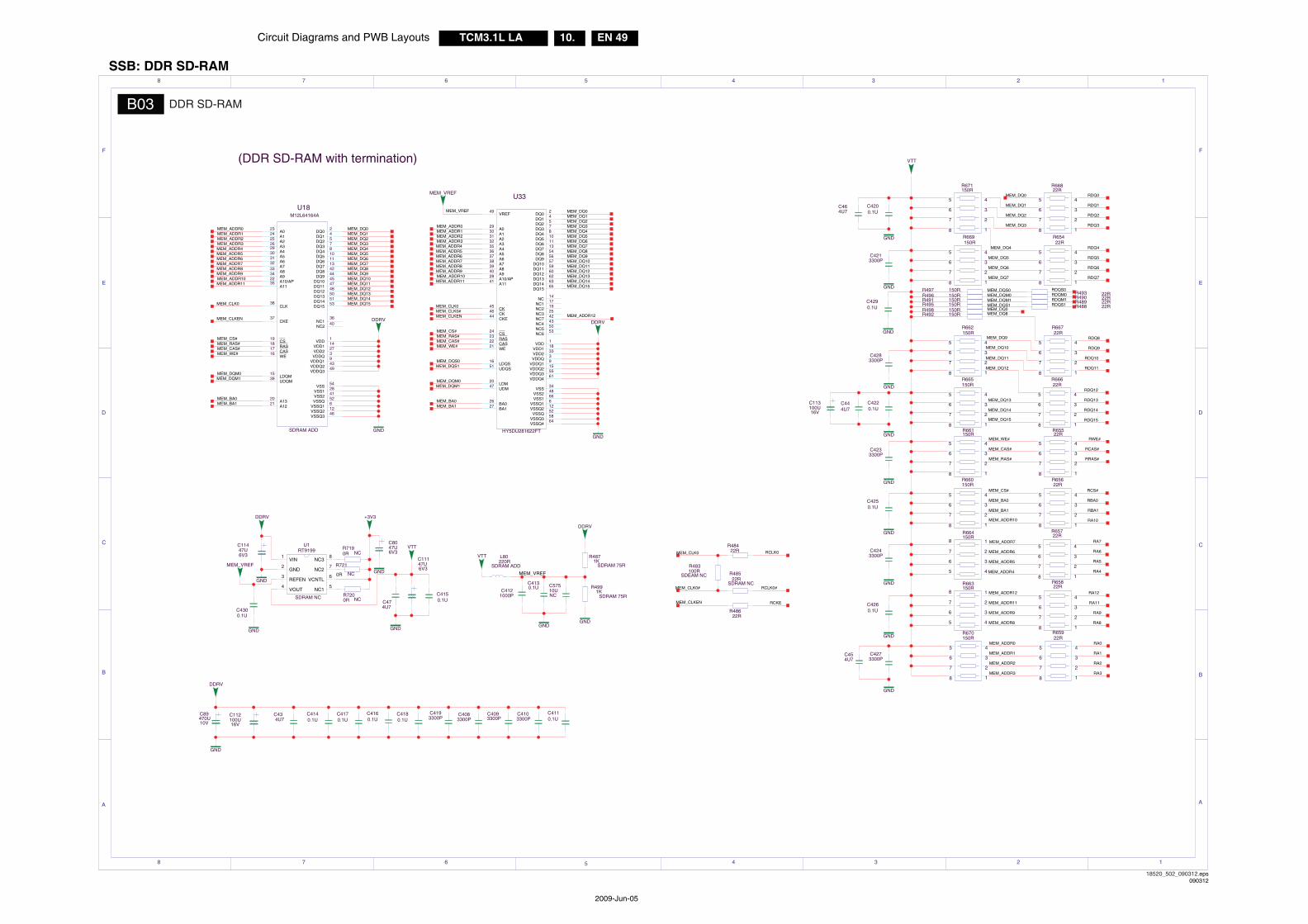
Circuit Diagrams and PWB Layouts EN 49TCM3.1L LA 10.
2009-Jun-05
SSB: DDR SD-RAM
GNDGND
GND
GND
GND
GND
GND
GND
GND
GND
GND
GND
GND
A
3 2 1
F
E
D
C
B
8 7 6 5
5
4 3 2 1
F
E
D
C
B
A
4678
GND
GND
GND
GNDGND
GND
REFEN VCNTL
NC1
NC3
VOUT
NC2
VIN
GND
A12
A0
A10/AP
A1
DQ9DQ10
DQ14
A4A5A6A7
A11
NC1CKE
CLK
UDQM
NC2
DQ0DQ1DQ2DQ3DQ4DQ5DQ6DQ7
VSS
A9
DQ12
VDD1
A3
RAS
A8
VDDQVDDQ1
LDQM
CAS
CS
A2
DQ8
DQ13
DQ15
WE
DQ11
A13
VSSQ2
VDD2
VDD
VDDQ2VDDQ3
VSSQ1VSSQ
VSS1VSS2
VSSQ3
WE
RASCAS
CS
CKE
CKCK
UDQS
A0A1A2A3A4A5A6A7A8A9A10/APA11
DQ0DQ1DQ2DQ3DQ4DQ5DQ6DQ7DQ8DQ9
DQ10DQ11DQ12DQ13DQ14DQ15
VSSQ
VSS
VSS1VSS2
NC
BA0BA1
VDDVDD1VDD2VDDQ
VDDQ1VDDQ2VDDQ3
NC1NC2NC3NC7NC4
VDDQ4
NC5NC6
LDQS
UDMLDM
VSSQ1VSSQ2
VSSQ3VSSQ4
VREF
(DDR SD-RAM with termination)
C89470U10V
C112100U16V
21
2322
24
44
4546
51
293031323536373839402841
245781011135456575960626365
52
34
6648
14
2627
11833391555
1719254243
61
5053
16
4720
612
5864
49
U33
HY5DU281622FT
C113100U16V
C11147U6V3
5 4
7 2
1
36
8
R671150R
5 4
7 2
1
36
8
R669150R
5 4
7 2
1
36
8
R662150R
5 4
7 2
1
36
8
R665150R
5 4
7 2
1
36
8
R661150R
5 4
7 2
1
36
8
R660150R
5 4
7 2
1
36
8
R664150R
5 4
7 2
1
36
8150RR663
5 4
7 2
1
36
8
R670150R
21
23
22
24
4445
51
29303132
35
3637
38
39
40
24578101113
54
34
48
14
26
18
33
39
15
17
19
25
42
50
53
16
47
20
12
27
1
4349
652
2841
46
U18M12L64164A
SDRAM ADD
R4991K
SDRAM 75R
R4871K
SDRAM 75R
VTT
C57510UNC
C434U7
C4130.1U
220RL80
SDRAM ADD2
3 6
5
8
4
7
1
U1RT9199
SDRAM NC
C8047U6V3
VTT
VTT
R48522R
SDRAM NC
R483100R
SDEAM NC
MEM_VREF
R497 150RR496 150RR491 150RR495 150RR498 150RR492 150R MEM_DQ8
MEM_DQ0
DDRV
6V347UC114
R7190R NC
R721
0R NC
R7200R NC
R48422R
R493 22R
5 4
7 2
1
36
8
R66822R
5 4
7 2
1
36
8
R66722R
5 4
7 2
1
36
8
R66622R
C4290.1U
R490 22RR489 22RR488 22R
C454U7
C444U7
C4283300P
C4273300P
C4260.1U
C4250.1U
C4243300P
C4233300P
C4220.1U
C4213300P
C4200.1U
C4193300P
C4180.1U
C4170.1U
C4160.1U
5 4
7 2
1
36
8
R65922R
5 4
7 2
1
36
8
R65822R
5 4
7 2
1
36
8
R65722R
5 4
7 2
1
36
8
R65622R
5 4
7 2
1
36
8
R65522R
5 4
7 2
1
36
8
R65422R
DDRV
C4140.1U
MEM_VREF
C4121000P
C4110.1U
DDRV
R48622R
C4103300P
C4093300P
C4083300P
DDRV
C464U7
DDRV
MEM_DQ3
MEM_DQM0MEM_DQM1
MEM_CLKEN
MEM_CLK0MEM_CLK0
MEM_CLK0
MEM_BA1MEM_BA0
MEM_DQ10
MEM_DQ11
MEM_DQ12
MEM_DQ0
MEM_DQ1
MEM_DQ2
MEM_DQ4
MEM_DQ9 RDQ8
MEM_DQ13
MEM_DQ14
MEM_DQ15
MEM_RAS#
MEM_DQ6
MEM_DQ5
MEM_VREF
MEM_DQ2MEM_DQ3
MEM_DQ6MEM_DQ7
MEM_DQ0MEM_DQ1
RWE#
MEM_ADDR10
RDQS1RDQM1
RDQS0RDQM0
MEM_DQS1MEM_DQM1MEM_DQM0MEM_DQS0
RCLK0
RCKE
MEM_CLK0#
RA5
RA6
RA7
MEM_ADDR5
MEM_ADDR6
MEM_ADDR7
MEM_CLKEN
MEM_DQS1
MEM_CLK0#
MEM_ADDR5MEM_ADDR4
MEM_ADDR6MEM_ADDR7MEM_ADDR8MEM_ADDR9
MEM_ADDR11
MEM_ADDR12
MEM_WE#MEM_CAS#MEM_RAS#MEM_CS#
MEM_ADDR10
MEM_DQ15MEM_DQ14MEM_DQ13MEM_DQ12MEM_DQ11MEM_DQ10MEM_DQ9MEM_DQ8
MEM_DQ5MEM_DQ4
MEM_ADDR3
MEM_ADDR1MEM_ADDR2
MEM_ADDR0
MEM_DQS0
RCLK0#
RDQ15
RDQ14
RDQ13
RDQ12
RRAS#
RCAS#
MEM_WE#
MEM_CAS#
RDQ9
RDQ10
RDQ11
RA8
RA9
RA11
RA12
RA3
RA2
RA1
RA0
MEM_ADDR3
MEM_ADDR2
MEM_ADDR1
MEM_ADDR0
RCS#
RBA0
RA10
MEM_BA1
MEM_BA0
MEM_CS#
RA4MEM_ADDR4
RBA1
MEM_DQ7
RDQ4
RDQ5
RDQ6
RDQ7
RDQ0
RDQ1
RDQ2
RDQ3
MEM_ADDR12
MEM_ADDR11
MEM_ADDR9
MEM_ADDR8
MEM_ADDR5MEM_ADDR4
MEM_ADDR6MEM_ADDR7MEM_ADDR8MEM_ADDR9
MEM_ADDR11MEM_ADDR10
MEM_ADDR3
MEM_ADDR1MEM_ADDR2
MEM_ADDR0
MEM_DQ2MEM_DQ3
MEM_DQ6MEM_DQ7
MEM_DQ0MEM_DQ1
MEM_DQ15MEM_DQ14MEM_DQ13MEM_DQ12MEM_DQ11MEM_DQ10MEM_DQ9MEM_DQ8
MEM_DQ5MEM_DQ4
MEM_BA1MEM_BA0
MEM_CLKEN
MEM_WE#MEM_CAS#MEM_RAS#MEM_CS#
MEM_DQM0MEM_DQM1
+3V3
C4300.1U
C474U7
C4150.1U
MEM_VREF
B03 DDR SD-RAM
18520_502_090312.eps090312
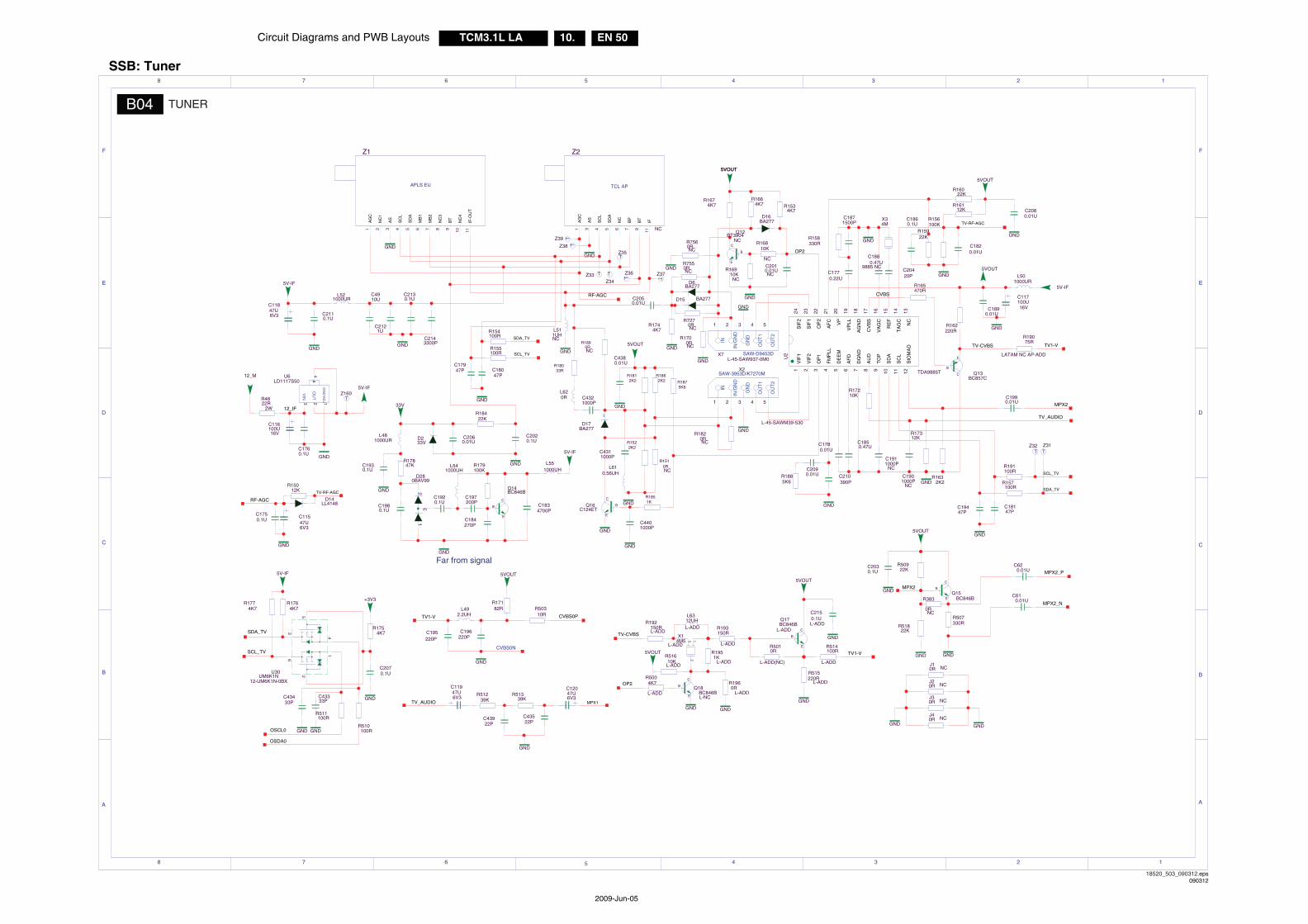
EN 50TCM3.1L LA 10.Circuit Diagrams and PWB Layouts
2009-Jun-05
SSB: Tuner
GND
GND
GND GND
GND
GND
GND
GND
GND
GND
GND
GND
GND
GND
TT
GND
GND
GND
GND
GND
GND
GND GND
GND
GND
GND
GND
A
3 2 1
F
E
D
C
B
8 7 6 5
5
4 3 2 1
F
E
D
C
B
A
4678
GND
T
GND
GN
D/A
DJ
OU
T
VIN
4
GND
GND
T
T
GND
GND GND
GND
GND GND
GND
GND
T
T T T
T
GND
AG
C
AS
SC
L
SD
A
NC
BP
BT
IFAG
C
NC
1
AS
SC
L
SD
A
MB
1
MB
2
NC
3
BT
NC
4
IF-O
UT
OU
T2
OU
T1
GN
D
IN/G
ND
IN
OU
T2
OU
T1
GN
D
IN/G
ND
IN
GND
GND
NC
TA
GC
RE
F
VA
GC
VIF
1
VIF
2
OP
1
FM
PLL
DE
EM
AF
D
DG
ND
AU
DC
VB
S
AG
ND
VP
LLVP
AF
C
SIF
1
SIF
2
OP
2
TO
P
SD
A
SC
L
SIO
MA
D
2
Far from signal
SAW-3953D/K7270M
SAW-D9453D
APLS EU TCL AP
CVBS0N
TV_AUDIO
SDA_TV
C11947U6V3
C2050.01U
D6BA277
D15 BA277
B
C
E
Q12BT3904
NC
R7550RNC
R7560RNC
6V347UC120
C1880.47U
9885 NC
13141516
1 2 3 4 5 6 7 817181920212324 22
9 10 11 12
U2
TDA9885T
R7270RNC
MPX1
R1960R
L-ADD
B
C
E
Q18BC846BL-NC
R192150RL-ADD
31 2 4 5
X7L-45-SAW937-0M0
54321
X2
L-45-SAWM39-530
3 12
X14M5
L-ADD
L6312UHL-ADD
R51610KL-ADD
R5010R
L-ADD(NC)
R514100R
L-ADD
C2010.01UNC
L610.56UH
C4311000P
R16910KNC
R16810K
NC
L511UHNC
0RR182
NC
R1744K7
R19075R
LATAM NC AP-ADD
1 2 3 4 5 6 7 8 9 10 11
Z1
1 3 4 5 6 7 9 11
Z2
NC
B
C
E
Q17BC846B
L-ADD
C1990.01U
R51339K
R51239K
X34M
C20420P
C117100U16V
C116100U16V
R5004K7
L-ADD
L551000UH
L541000UH
R383
0RNC
R158330R
R515220R
L-ADD
D16BA277
D17BA277
CVBS0P10RR503
5VOUT
5VOUT
5V-IF
82RR171
L492.2UH
220RR162
TV-CVBS
470RR165
B
C
EQ15
BC846B
TV1-V
C195220P
Z35
Z37
Z34Z33
RF-AGC
Z39
L521000UR
J10R NC
R507330R
R51822K
12_IF
C1890.01U
B
C
E
Q13BC857C
TV1-V
R50922K
Z38
Z36
C1911000P
NC
C1901000P
NC
R1510RNC
C2150.1UL-ADD
R193150R
L-ADD
R1951K
L-ADD
L620R
R1890RNC
R1700RNC
2
63
5
41
U30UM6K1N
12-UM6K1N-0BX
R1851K
B
C
E
Q14BC846B
C2060.01U
R18422K
C2020.1UD2
33V
SCL_TV
MPX2_P
MPX2_N
SDA_TV
SCL_TV
OSDA0
OSCL0
TV_AUDIO
TV1-V
CVBS
TV-RF-AGC
4
123
U6LD1117S50
0.47UC185
C2090.01U
5VOUT
C610.01U
C620.01U
C2030.1U
R4822R
2W
Z160
TV-CVBS
5VOUT
C11547U6V3
C11847U6V3
5VOUT
R191100R
5V-IF
5V-IF
5VOUT
5V-IF
C2143300P
0.1UC213
C2121U
C4910U
C2110.1U
C210390P
R1885K6
R1875K6
R1862K2
C4401000P
C43922P
33V
C2080.01U
C2070.1U
C4380.01U
R1812K2
R18033R
R179100K
R511100R
R510100R
R17847K
R1774K7
R1764K7
Z32 Z31
+3V3
R1754K7
5V-IF
R17312K
R17210K
L501000UR
5VOUT5VOUT
C1980.1U
C197200P
R1674K7
R1664K7
C196220P
5VOUT
C19447P
C1930.1U
C1920.1U
R1632K2
R16112K
R16022K
C1871500P
R15922K
C1860.1U
C184270P
C1834700P
L481000UR
R157100R
R156100K
C1820.01U
C18147P
R155100R
R154100R
C18047P
C17947P
C1780.01U
1
3
2
D280BAV99
C1770.22U
R1534K7
C43522P
C43433P 33P
C433
R1522K2
C4321000P
12_M
0.1UC176
GND
12KR150
LL4148D14
0.1UC175
OP2
MPX2
SDA_TV
SCL_TV
TV-RF-AGC
RF-AGC
OP2
B
C
E
C124ETQ16
MPX2
J20R NC
J30R NC
J40R NC
B04 TUNER
18520_503_090312.eps090312
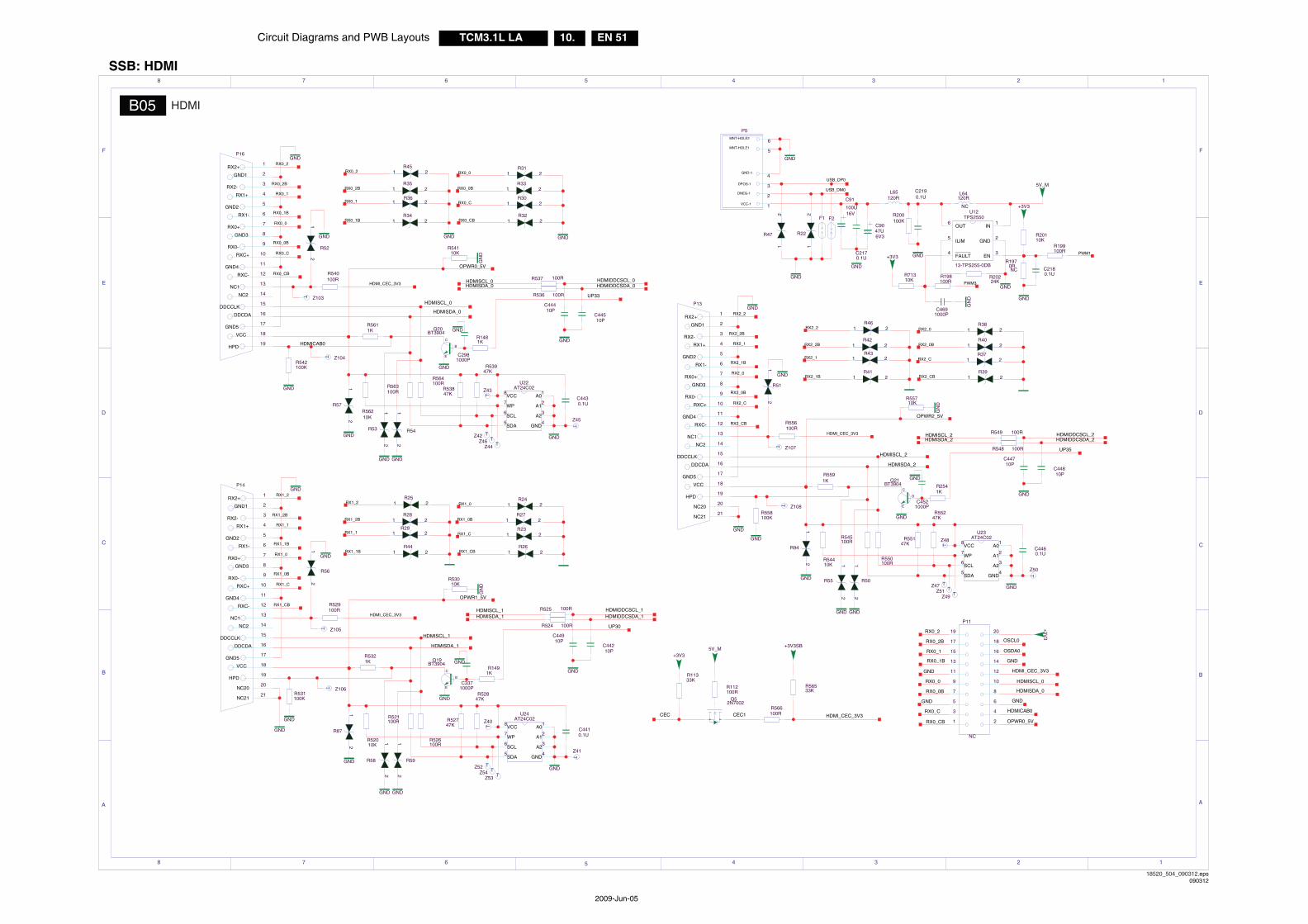
Circuit Diagrams and PWB Layouts EN 51TCM3.1L LA 10.
2009-Jun-05
SSB: HDMI
TT
T
GNDGND
GND
GND
GND
GND
GND
GND
GND
GND
T
GN
D
GND
GND
GND
GNDT
T
T
T
T
GN
D
GND
GND
GNDT
T
T
T
T
SDA
SCL
WP
VCC
GND
A2
A1
A0
GN
D
GND
GND
GND
GND
GND GND
GND
GND
GNDT
TT
SDA
SCL
WP
VCC
GND
A2
A1
A0
GNDGND
A
3 2 1
F
E
D
C
B
8 7 6 5
5
4 3 2 1
F
E
D
C
B
A
4678
GND
GND
GND
GND
GND
GND
GN
D
GND
VCC-1
DNEG-1
DPOS-1
GND-1
MNT-HOLE1
MNT-HOLE2
GND
GND
GND
GND
TT
T
GND
OUT
FAULT
ILIM
EN
GND
IN
NC21
GND1
RX2-
RX1+
GND2
RX1-
RX0+
GND3
RX0-
RXC+
GND4
RXC-
NC1
NC2
DDCCLK
DDCDA
GND5
VCC
RX2+
HPD
NC20
SDA
SCL
WP
VCC
GND
A2
A1
A0
NC21
GND1
RX2-
RX1+
GND2
RX1-
RX0+
GND3
RX0-
RXC+
GND4
RXC-
NC1
NC2
DDCCLK
DDCDA
GND5
VCC
RX2+
HPD
NC20
T
RX2+
GND1
RX2-
RX1+
GND2
RX1-
RX0+
GND3
RX0-
RXC+
GND4
RXC-
NC1
NC2
DDCCLK
DDCDA
GND5
VCC
HPD
HDMISCL_2HDMISDA_2
UP35
UP30
HDMISDA_1HDMISCL_1
UP33
HDMISCL_0HDMISDA_0
1
2
3
4
5
6
7
8
9
10
11
12
13
14
15
16
17
18
19
P16
Z40
21
2
3
4
5
6
7
8
9
10
11
12
13
14
15
16
17
18
1
19
20
P13
1 2
4
6
8
12
14
16
18
20
10
3
5
7
9
11
13
15
17
19
P11
NC
5
6
7
8
4
3
2
1
U22AT24C02
HDMIDDCSCL_0HDMIDDCSDA_0
R529100R
21
R56
21
2
3
4
5
6
7
8
9
10
11
12
13
14
15
16
17
18
1
19
20
P14
21R26
21R23
21R27
21R24
21R44
21R29
21R28
21R25
B
C
E
Q19BT3904
HDMISCL_1
HDMIDDCSCL_1HDMIDDCSDA_1
R56533K
R11333K
C9047U6V3
C91
100U16V
L65120R
L64120R
NC
6
4
5
3
2
1
U12TPS2550
13-TPS255-0DB
R20224K
R540100R
CEC1CEC
USB_DP0
Z105
Z106
Z104
R112100R
Q52N7002
C2180.1U
R199100R
R198100R
C4691000P
1KR254
C4521000P
C3371000P
C2981000P
1KR149
HDMISDA_0
B
C
E
Q20BT3904
1KR148
1
2
3
4
5
6
P5
RX0_1B 21R32
21R30
21R33
21R31
21R34
21R36
21R35
21R45
12
R22
21
R47
21R39
21R37
21R40
21R38
21R41
21R43
21R42
21R46
21
R52
PWM3
HDMISCL_0
R71310K
B
C
E
Q21BT3904
HDMIDDCSCL_2
USB_DM0
HDMI_CEC_3V3
R556100R
HDMISCL_0
HDMISDA_0
R566100R
OPWR0_5V
HDMICAB0
GND
RX0_2
RX0_2B
RX0_1
RX0_1B
GND
RX0_0
RX0_0B
GND
RX0_C
RX0_CB
+3V
3OPWR0_5V
1KR561
HDMI_CEC_3V3
HDMI_CEC_3V3
OSCL0
+3V35V_M
+3V3SB
HDMISCL_2
OPWR1_5V
21
R53
1KR532
R20110K
+3V3
5V_M
R1970RNC
PWM1
HDMISDA_2
21
R54
21
R50
21
R55
21
R59
RX1_1
RX1_2
RX1_0B
RX1_C
R558100K
21
R585
6
7
8
4
3
2
1
U24AT24C02
Z54Z53
Z52
21
R51100RR564
R563100R
R56210K
C44910P
1KR559
10KR557
5
6
7
8
4
3
2
1
U23AT24C02
R55247K
R55147K
Z51
100RR550
10PC448
C44710P
R549 100R
100RR548
Z50
Z49
R545100R
R54410K
C4460.1U
Z48
Z47
R542100K
10KR541
R53947K
R53847K
Z46
10PC445
C44410P
R537 100R
100RR536
Z45
Z44
C4430.1U
Z43
Z42
R531100K
10KR530
R52847K
R52747K
100RR526
10PC442
R525 100R
100RR524
Z41
R521100R
R52010K
C4410.1U
C2190.1U
R200100K
0.1UC217
RX2_2
RX0_2 RX0_0
RX0_1
RX0_0B
RX0_CB
RX1_2B
RX1_1B
RX1_0
RX1_CB
RX1_2B
RX1_2
RX1_1
RX1_0
RX1_0B
RX1_C
RX1_CB
HDMI_CEC_3V3
HDMISDA_1
RX1_1B
RX0_2B
RX0_C
HDMI_CEC_3V3
RX2_CB
RX2_C
RX2_0B
RX2_0
RX2_1
RX2_2
RX2_2B
RX2_CB
RX2_C
RX2_0B
RX2_1
RX2_0
RX2_1B
RX2_2B
RX2_1B
HDMIDDCSDA_2
RX0_CB
RX0_C
RX0_0B
RX0_0
RX0_1B
RX0_1
RX0_2B
RX0_2
+3V3
21
R57
21
R87
21
R94
OPWR2_5V
F1 F2
GND
OSDA0
Z103
HDMICAB0
Z107
Z108
B05 HDMI
18520_504_090312.eps090312
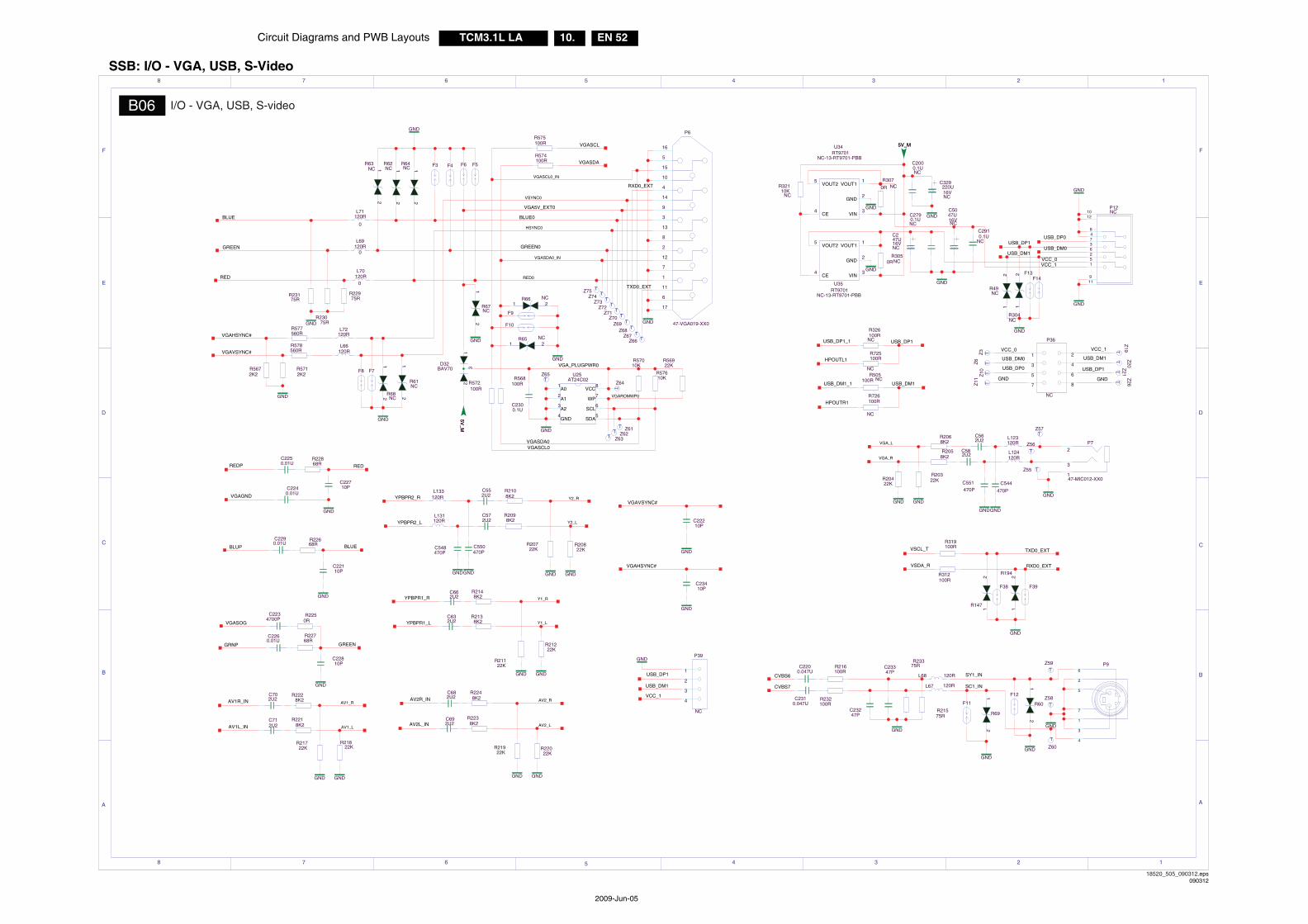
EN 52TCM3.1L LA 10.Circuit Diagrams and PWB Layouts
2009-Jun-05
SSB: I/O - VGA, USB, S-Video
GND
GNDGND
GND
GNDGND
GND
GND
GND
GND
GND
GNDGND
T
GND
T
GND GNDGNDGND
GND
GND
GND
GND
GND
GND
GNDT
TT
T
T
GND
SDA
SCL
WP
VCC
GND
A2
A1
A0
GND
TT
TT
TT
TT
TT
GND
GND
GND
GND
GND
GND
A
3 2 1
F
E
D
C
B
8 7 6 5
5
4 3 2 1
F
E
D
C
B
A
4678
T
T
T
GND
GND
GND
GND
VOUT2
CE VIN
GND
VOUT1
GNDGND
GND
T
GND
TT
TT
TT
TT
VOUT2
CE VIN
GND
VOUT1
1
2
3
4
P39
NC
4
3
1
7
5
2
6P9
3
1
2P7
47-MIC012-XX0
6
4
11
14
15
7
12
8
5
13
3
10
9
1
2
16
17
P6
47-VGA019-XX0L72
120R
L71120R
0
L70120R
0
L69120R
0
L68 120R
L67 120R
L66120R
120RL133
L131120R
L124120R
L123120R
16V
C247U
NC
NC0R
R307 C329220U16VNC
0.1UC200
NC
C2790.1UNC
5
4 3
2
1
U35RT9701
NC-13-RT9701-PBB
VCC_1
0.1UC291
NC
21R65 NC
21R66 NC
21
R61NC
21
R68NC
21
R67NC
21
R64NC
21
R62NC
21
R63NC
R3050RNC
1 2
3 4
5 6
7 8
P36
NC
R505100R NC
R326100R
NC
Z3
Z6
Z10
Z11
Z26
Z21
Z19
Z20
HPOUTR1
TXD0_EXT
TXD0_EXT
RXD0_EXT
RXD0_EXT
VSYNC0
VGASCL0_IN
F9
VGAROMWP0
R312100R
R319100R
VSDA_R
VSCL_T
R56922K
Z57
VCC_1
SC1_INR2248K2
5V_M5V_M
USB_DM1
USB_DP1
USB_DP1
VGASOG
R2068K2
R2058K2
VGA_L
R2108K2
R2098K2
R2228K2
R2218K2
R2238K2
R2138K2
R2148K2
GRNP
VGA_R
VGASDA0
C23410P
R568100RR572
100R
R57010K
R20422K
VGASCL0
VGASDA0_IN
VGASDA
R20322K
21
R49NC
12
R304NC
F13F14
8
7
5
4
3
1
62
911
1012
P12NC
47UC50
16VNC
R32110K
NC
5
4 3
2
1
U34RT9701
NC-13-RT9701-PBB
VGAHSYNC#
C22210P
VGAVSYNC#
C22810P
C22710P
C22110P
USB_DM1
R726100R
NC
R725100R
NC
BLUE
HPOUTL1
VCC_1VCC_0
USB_DM1USB_DM0
USB_DP1USB_DP0
GNDGND
USB_DP0
USB_DM0
R22668R
C2290.01U
R2250R
C2234700P
R22768R
C2260.01U
C712U2
C702U2
C2240.01U
C2250.01U
C2310.047U
C2200.047U
R216100R
F10R577560R
F5F6
RED0
C562U2
C582U2
C552U2
C572U2
AV2R_INC682U2
AV2L_INC692U2
C662U2YPBPR1_R
YPBPR1_L 2U2C63
R21122K
R21222K
R22022K
R21922K
R21822K
R21722K
AV1L_IN
AV1R_IN
12
3
D32BAV70
Z55
Z56
12
R60
Z60
USB_DP1_1
12
R69
USB_DM1_1
R578560R
R23375RC233
47P
C23247P
R232100R
R57610K
Z75Z74
Z73Z72
Z71Z70
Z69Z68
Z67Z66
1
2
3
4
6
5
8
7
U25AT24C02
R575100R
R574100R
R5712K2
R5672K2
R23175R
R23075R
R22975R
C2300.1U
Z65
Z64
Z63Z62
Z61
5V_M
5V_M
R22868R
Z59
Z58
R21575R
VGAVSYNC#
VGAHSYNC#
RED
CVBS7
Y1_R
RED
GREEN
VGA_PLUGPWR0
VGASCL
REDP
VGAGND
GREEN
BLUEBLUP
AV1_R
AV1_L
AV2_R
AV2_L
CVBS6
Y1_L
C551470P
C544
470P
R20722K
R20822K
F3 F4
BLUE0
GREEN0
VGA5V_EXT0
F7F8
HSYNC0
F11
F12
USB_DP1
USB_DM1
SY1_IN
Y2_L
Y2_R
YPBPR2_L
YPBPR2_R
470PC550
470PC548
21
R147
F38
21
R194
F39
VCC_0
B06 I/O - VGA, USB, S-video
18520_505_090312.eps090312
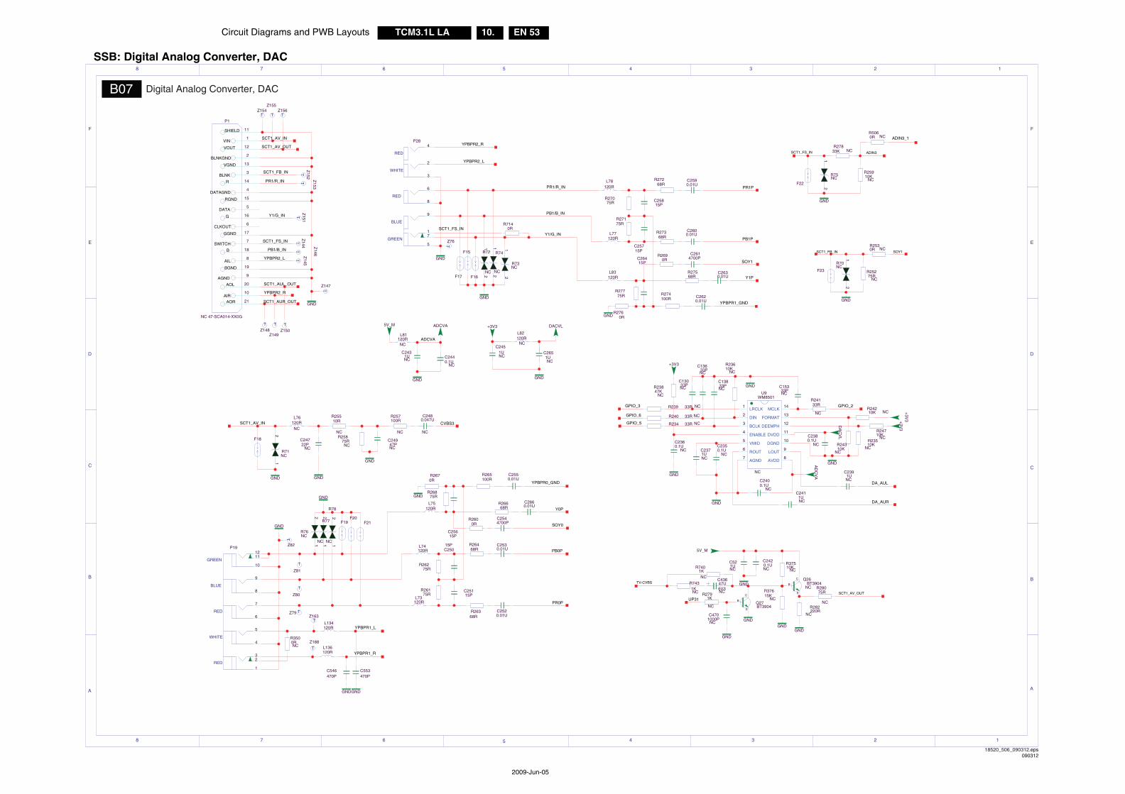
Circuit Diagrams and PWB Layouts EN 53TCM3.1L LA 10.
2009-Jun-05
SSB: Digital Analog Converter, DAC
GND
T
GND
GND
GND
GND
GND
T
GND
T
T
T
T
GND
GND
GND
GREEN
BLUE
RED
WHITE
RED
GND GND
GND
GND
GNDGND
TTT
TT
TT
TT
T
TT
GND
GND
GND
GND
GND
GND GND
LRCLK
DIN
BCLK
ENABLE
VMID
ROUT
AGND
DGND
DVDD
DEEMPH
FORMAT
MCLK
LOUT
AVDD
GND
GND
AORAIR
AOL
AGND
BGND
AIL
B
SWITCH
GGND
CLKOUT
G
DATA
RGND
DATAGND
R
BLNK
VGND
BLNKGND
VOUT
VIN
SHIELD
RED
GREEN
BLUE
WHITE
RED
A
3 2 1
F
E
D
C
B
8 7 6 5
5
4 3 2 1
F
E
D
C
B
A
4678
T
T
Z188
Z163
120RL136
B
C
E
Q26BT3904
NC
C43647U6V3NC
71
5
9
8
6
3
2
4P28
21
10
20
9
19
8
18
7
17
6
16
5
15
4
14
3
13
2
12
1
11
P1
NC 47-SCA014-XX0G
R37615K
NC
L83120R
L82120R
NC
L81120RNC
L78120R
L77120R
L76120RNC
L75120R
L74120R
L73120R
L134120R
C2480.047U
NC
R257100R
NC
C24947PNC
R25875RNC
R25510R
NC
C24722P
NC
21
R71NC
21
R76NC
21
R77
NC
21
R78
NC
21
R74
NC
21
R72
NC
21
R73NC
R28075R
NCR282220R
NCC4701000PNC
R2791K
NC
R7431KNC
R7401KNC
0.1UC242
NC
C521UNC
R24133R
NC
TV-CVBS
C2651UNC
SCT1_AV_OUT
10KR375
NC
UP31
DA_AUL
C2391UNC
AD
CV
A
C2400.1U
NC
R2600R
R24710K
NCC2380.1U
NC10KR243
NC
R23510K
NC
R24210K NC
C2411UNC
C15333PNC
1
2
3
4
5
6
7
10
11
12
13
14
9
8
U9WM8501
NC
C2350.1U
NCC2371UNC
C2360.1U
NC
R23610K
NC
C13833PNC
C13633PNC
C13033PNCR238
47KNC
R234 33R NC
R240 33R NC
R239 33R NC
C2451UNCC244
0.1UNC
C2431UNC
21
R70NC
R25275R
NC
R2530R NC
21
R75NC
R5060R NC
R25910K
NC
R27833K NC
R7140R
YPBPR0_GND
PR1P
R27568R
R2690R
R27368R
R27268R
C2590.01U
C2600.01U
C2620.01U
C2630.01U
C2614700P
R274100R
R265100R
R26368R
R26468R
R26668R
C2550.01U
F19 F21
F23
SCT1_FB_IN
F22
SCT1_FS_IN
F17 F16
F15
PR1/R_IN
PB1/B_IN
B
C
E
Q27BT3904
YPBPR1_GND
YPBPR2_L
YPBPR2_R
Z148 Z150
Z147
Z145
Z146
Z144
Z151
Z153
Z152
Z154Z155
Z156
YPBPR1_L
YPBPR1_R
PR1/R_IN
GPIO_6
GPIO_5
GPIO_3
+3V3
GPIO_2
ADIN3_1
1
23
4
5
6
7
8
9
10
1112
P19
C2660.01U
5V_M
5V_M +3V3
Z82
Z81
Z80
Z79
Z76
C26415P
R27775R
R2760R
C25815P
C25715P
R27175R
R27075R
C25615P
R26875R
R2670R
C2544700P
C2530.01U
C2520.01U
C25115P
C25015P
R26275R
R26175R
ADCVA DACVL
+3V
3+
3V3
DA
CV
L
PB0P
SCT1_FS_IN
PB1/B_IN SOY1
SCT1_FB_IN
Y1/G_IN
YPBPR2_L
PR0P
ADIN3
CVBS3
ADCVA
PB1P
SOY1
Y1P
SCT1_AV_IN
SCT1_AV_OUT
SCT1_AUR_OUT
SCT1_AUL_OUT
C553470P
C546470P
YPBPR2_R
Z149
Y0P
SOY0
SCT1_FS_INY1/G_IN
F18
SCT1_AV_IN
F20
R3500RNC
DA_AUR
B07 Digital Analog Converter, DAC
18520_506_090312.eps090312
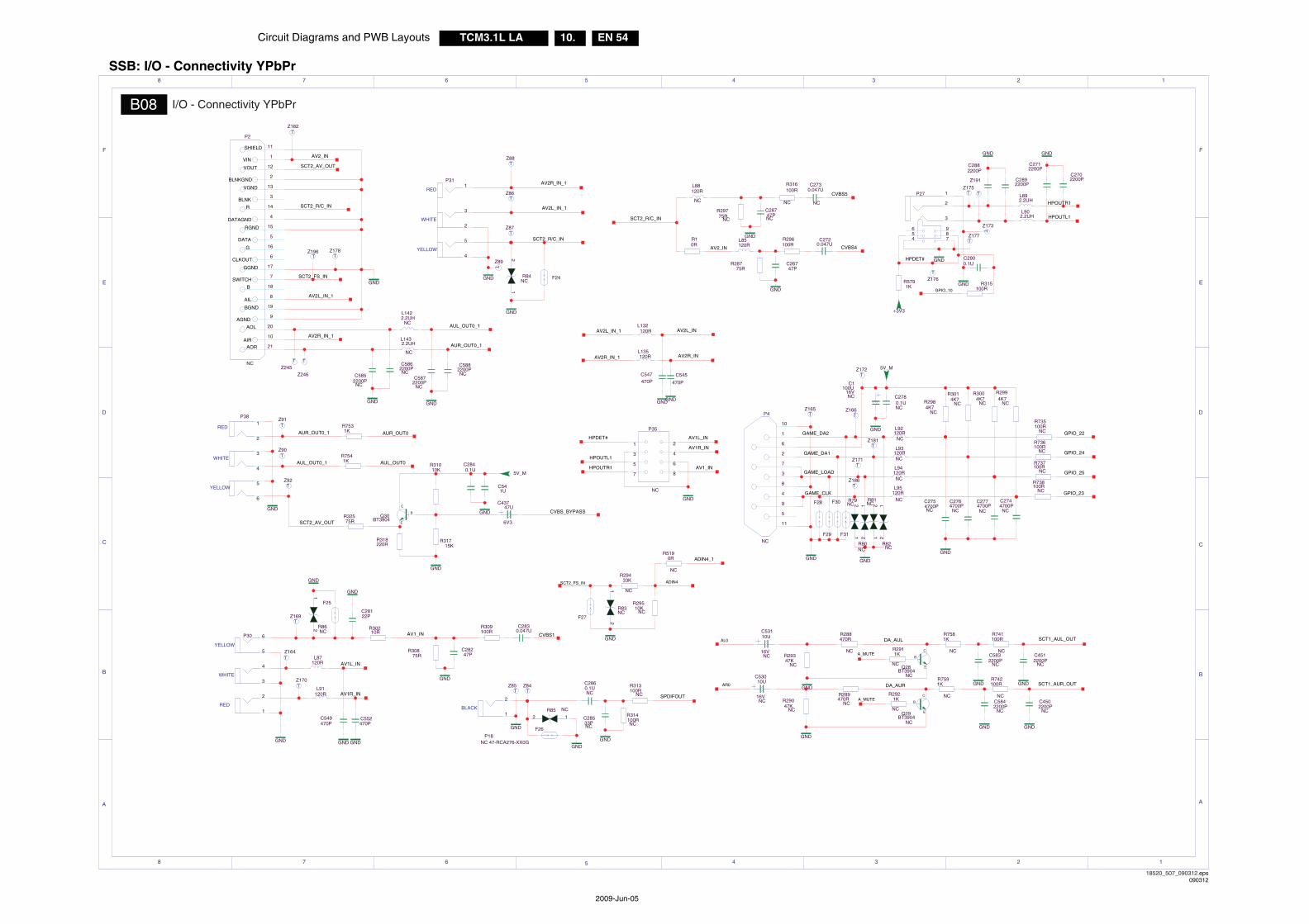
EN 54TCM3.1L LA 10.Circuit Diagrams and PWB Layouts
2009-Jun-05
SSB: I/O - Connectivity YPbPr
GND
T
T
T
T
T
T
GND
GND
GND
GND
GND
GND
GND
GND
GND
GND
TT
T
T
T
GND
T
GND
T
T
GND
GND
GND
GND
T
T
TT
T
GND
GND
GND
T
GND
T
GND
GND
T
GND
GND
GND
T
T
GND GND
GND
A
3 2 1
F
E
D
C
B
8 7 6 5
5
4 3 2 1
F
E
D
C
B
A
4678
GND
RED
WHITE
YELLOW
WHITE
RED
YELLOW
BLACK
GND
AORAIR
AOL
AGND
BGND
AIL
B
SWITCH
GGND
CLKOUT
G
DATA
RGND
DATAGND
R
BLNK
VGND
BLNKGND
VOUT
VIN
SHIELD
GND
GND
T
T
T
GND
GND
RED
WHITE
YELLOW
T
GND
GND
AV2L_IN_1
AV2R_IN_1
R7591K
NC
R7581K
NC
SCT1_AUL_OUT
C5832200P
NC
R742100R
NC
2200PC584
NC
Z245
B
C
EQ28BT3904
NC
R2911K
NC
R2921K
NC
B
C
EQ29BT3904
NC
1
4
2
5
3
6
P38
R7531K
R7541K AUL_OUT0
AUR_OUT0
AUL_OUT0_1
AUR_OUT0_1L1432.2UH
NC
L1422.2UH
NC
C5882200PNC
C5872200P
NC
C5862200PNC
C5852200PNC
R741100R
NC
2200PC450
NC
C4512200P
NC
Z92
Z246
SCT2_FS_IN
Z196
C2882200P
L892.2UH
SCT1_AUR_OUT
R32575R
21
10
20
9
19
8
18
7
17
6
16
5
15
4
14
3
13
2
12
1
11
P2
NC
R316100R
NC
R29775R
NC
C2730.047U
NC
C28747PNC
1
2
P18NC 47-RCA276-XX0G
1
4
2
5
3
P31
R10R
SCT2_R/C_IN
47PC267
C2720.047U120R
L85
75RR287
R296100R
1
4
2
5
3
6P30
R738100R
NC
R737100R
NC
R736100R
NC
R735100R
NC
C2754700PNC
C2764700PNC
C2774700PNC
C2744700PNC
R2994K7
NC
R3004K7
NC
R3014K7
NCR2984K7
NC
16V100U
C1
NC C2780.1UNC
L92120R
NC
L93120RNC
L94120RNC
L95120R
NC
21
R82NC
21
R81NC
21
R80NC
21
R79NC
6
1
7
2
3
8
9
5
4
10
11
P4
NC
L88120R
NC
21
R83NC
R29510K
NC
R29433K
NC
R5190R
NC
R289470R
NC
R288470R
NCR29347K
NC
R29047K
NC
C53010U
16VNC
C53110U
16VNC
C2860.1UNC
R313100R
NC
R314100RNC
C28533PNC
2 1R85 NC
SPDIFOUT
1 2
3 4
5 6
7 8
P35
NC
R31715K
C43747U
6V3
L91120R
120RL87
L135120R
L132120R
21
R86NC
21
R84NC
AV1L_IN
R31010K
GPIO_23
GPIO_25
GPIO_24
GPIO_22
ADIN4_1
C552470P
C549470P
AV1R_IN
Z170
CVBS_BYPASS
R318220R
Z164
7
654
89
3
1
2
P27
HPOUTL1
HPOUTR1
R315100R
C2900.1U
GAME_LOAD
HPDET#
C2892200P
AR0
AL0
C2830.047U
R309100R
F31
F30
F25
SCT2_R/C_IN
A_MUTE
F28
Z165
F26
A_MUTE
Z177
Z173
AV2R_INAV2R_IN_1
AV2L_INAV2L_IN_1
AV2R_IN_1
AV2L_IN_1SCT2_R/C_IN
5V_M
SCT2_AV_OUT
ADIN4
C545
470P
C547470P
Z178
Z175
Z191
Z186
Z182
AV2_IN
C28122P
10RR302
L902.2UH
5V_M
1KR579
+3V3
Z91
Z90
Z89
Z88
Z87
Z86
Z85 Z84
0.1UC284
C541U
B
C
E
Q30BT3904
R30875R
C28247P
C2712200P
C2702200P
GPIO_10
CVBS5
CVBS4
AV2_IN
Z169
Z166
Z172
Z181
Z171
Z176F24
F27
SCT2_FS_IN
F29
GAME_CLK
GAME_DA1
GAME_DA2HPDET#
HPOUTR1
HPOUTL1
AV1_IN
AV1R_IN
AV1L_IN
AV1_IN CVBS1
SCT2_AV_OUT
AUR_OUT0_1
AUL_OUT0_1
DA_AUR
DA_AUL
B08 I/O - Connectivity YPbPr
18520_507_090312.eps090312
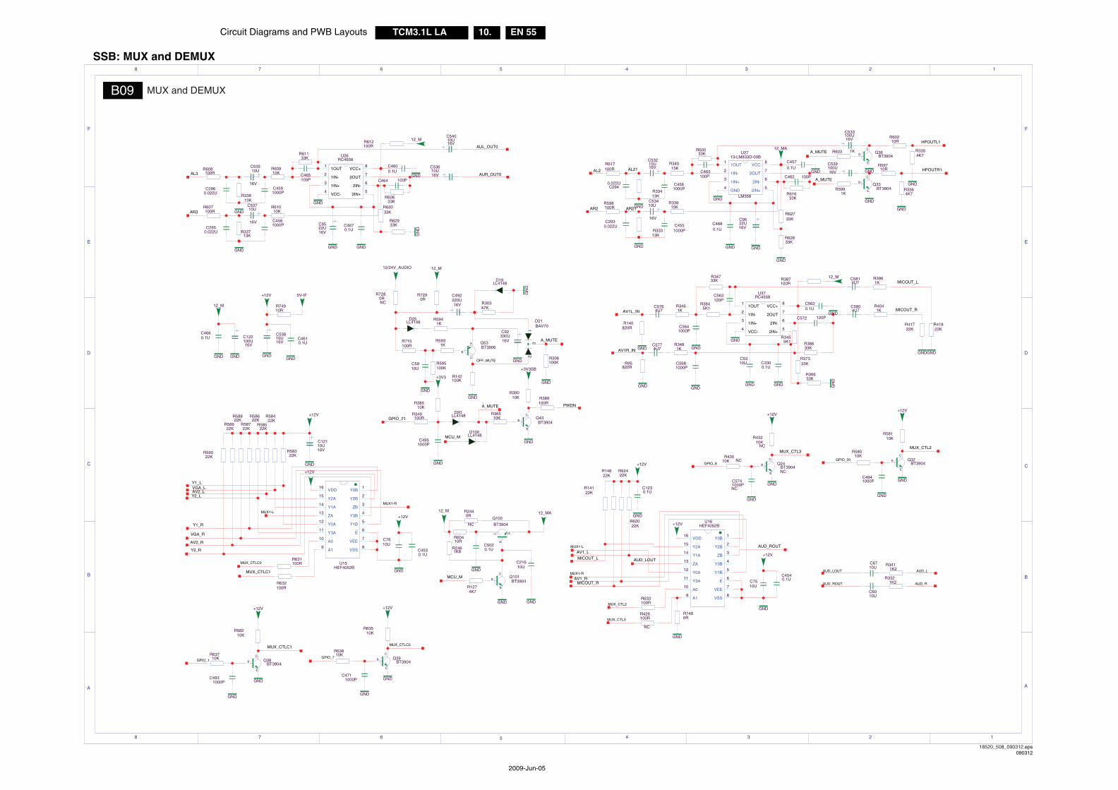
Circuit Diagrams and PWB Layouts EN 55TCM3.1L LA 10.
2009-Jun-05
SSB: MUX and DEMUX
GND
GND
GND
GND
GND
2IN+
2IN-
2OUT
VCC+
1IN+
1IN-
1OUT
VCC-
GND
GND
GN
D
GND
GND
GND
GN
D
GND
GND
GND
GND
GND
GND
GNDGND
GND
GND
GND
GND
GND
GND
GND
GND
GND
2IN+
2IN-
2OUT
VCC+
1IN+
1IN-
1OUT
VCC-
GND GND GND
GND
GNDGND
GND
GND
GND
GND
GND
GND
GND
GND
GND GND
GND
GND
GND
GND
GND
GND
GND
GNDGND
Y0B
Y2B
ZB
Y3B
Y1B
E
VEE
VSSA1
A0
Y3A
Y0A
ZA
Y1A
Y2A
VDD
GN
D
GND
A
3 2 1
F
E
D
C
B
8 7 6 5
5
4 3 2 1
F
E
D
C
B
A
4678
Y0B
Y2B
ZB
Y3B
Y1B
E
VEE
VSSA1
A0
Y3A
Y0A
ZA
Y1A
Y2A
VDD
VCC
2OUT
2IN-
GND 2IN+
1IN+
1IN-
1OUT
AUL_OUT0
AUR_OUT0
B
C E
Q100
BT3904
R60410R
C92330U16V
C492220U16V
R7290R
R7280RNC
B
C
E
Q24BT3904NC
C5741000PNC
R7480R
R426100R
NC
R43510K NC
R43210K
NC
R3461K
C5764U7
AV1R_IN
C5620.1U
C572 120P
R36633K
R38633K
R37333K
R3455K1
R41822K
R41722K
R4041K
C5804U7
R3961K
C5814U7
R387100R
R33915K
R34015K
R60033K
8
7
6
4 5
3
2
1
U2713-LM833D-00B
LM358
C53510U
16V
C53710U
16V
C53210U16V
C53410U
16V
C539100U16V
+12V
C5774U7
R95820R
R140820R C564
1000P
C1230.1U
1
2
3
4
5
6
7
89
10
11
12
13
14
15
16
U16HEF4052B
C4540.1U
12_M
R2461K8
5V-IF+12V
R74910R
MICOUT_L
MUX1-L
C9522U16V
C9622U16V
C54010U16V
AV1_L
AV1_RMICOUT_R
MUX1-R
Y1_R
Y1_L
AV2_L
AV2_R
C6710U
R3411K2
R3321K2
Y2_L
VGA_L
MUX1-L
VGA_R
12_M
PWDN
R62933K
1
2
3
4
5
6
7
89
10
11
12
13
14
15
16
U15HEF4052B
+12V
10UC216
A_MUTE
MUX_CTL3MUX_CTL2
AV1L_IN
R3481K
R34733K
C5310U
MUX_CTL2
R633100R
B
C
E
Q32BT3904
+12V
R14622K
R14122K
+12V
GPIO_21
R62422K
12_MA
C5020.1U
R2440R
NC
12_MA
MCU_M
+12V
AR21
AL21
C2930.022U
R617100R
B
C
E
Q101BT3904
R1274K7
MCU_M
AUD_LOUT
R62022K
12_M
C4610.1U
10UC59
R38510K
R36510K
B
C
E
Q43BT3904
12
3
D21BAV70
D20LL4148R349
100R
R389100R
C4941000P
R58010K
C4711000P
R63710K
R63810K
R142100K
12_M12/24V_AUDIO
R715100R
R58322K
R58422K
R58522K
R58622K
Y2_R
C4660.1U C122
100U16V
C53810U16V
R306100K
B
E
C
Q53BT3906
D19LL4148
R30347K
R5941K
D25LL4148
R5931K
R595100K
R39010K
R58210K
B
C
E
Q38BT3904
R63510K
B
C
E
Q39BT3904
MUX_CTLC1
GPIO_7GPIO_1
R632100R
R631100R
HPOUTR1
HPOUTL1
AL2
C2940.022U
C533100U16V
R3364K7
R612100R
A_MUTE
A_MUTE
R60210R
R59710R
R3354K7
R59022K
R58922K
R58822K
R58722K
AUD_ROUT
OFF_MUTE
C12110U16V
MUX_CTLC0
+3V3SB
R598100R
C2950.022U
C2960.022U
+12V
+12V
+12V
+12V+12V
C7610U
C7510U
C4680.1U
C4670.1U
R63033K
R62833K
R62733K
5
6
7
8
3
2
1
4
U26RC4558
B
C
E
Q36BT3904
C465100P C464 100P
C463100P C462 100P
R61633K
C4600.1U
R61133K
C53610U16V
R61010K
R60910K
C4591000P
R608100R
R33813K
C4581000P
R607100R
R33713K
R60633K
R603 1K
C4570.1U
B
C
E
Q33BT3904R599
1K
C4561000P
R33413K
C4551000PR333
13K
C4530.1U
R58110K
MUX_CTLC1
MUX1-R
AR2
MUX_CTLC0
C4931000P
+3V3
C4951000P
D100LL4148
A_MUTE
AR3
AL3
12_M
R3845K1
C5681000P
C563120P
C3300.1U
5
6
7
8
3
2
1
4
U37RC4558
C6010U
AUD_LOUT
AUD_R
AUD_L
AUD_ROUT
MUX_CTL3
MICOUT_R
MICOUT_L
GPIO_20GPIO_8
B09 MUX and DEMUX
18520_508_090312.eps090312
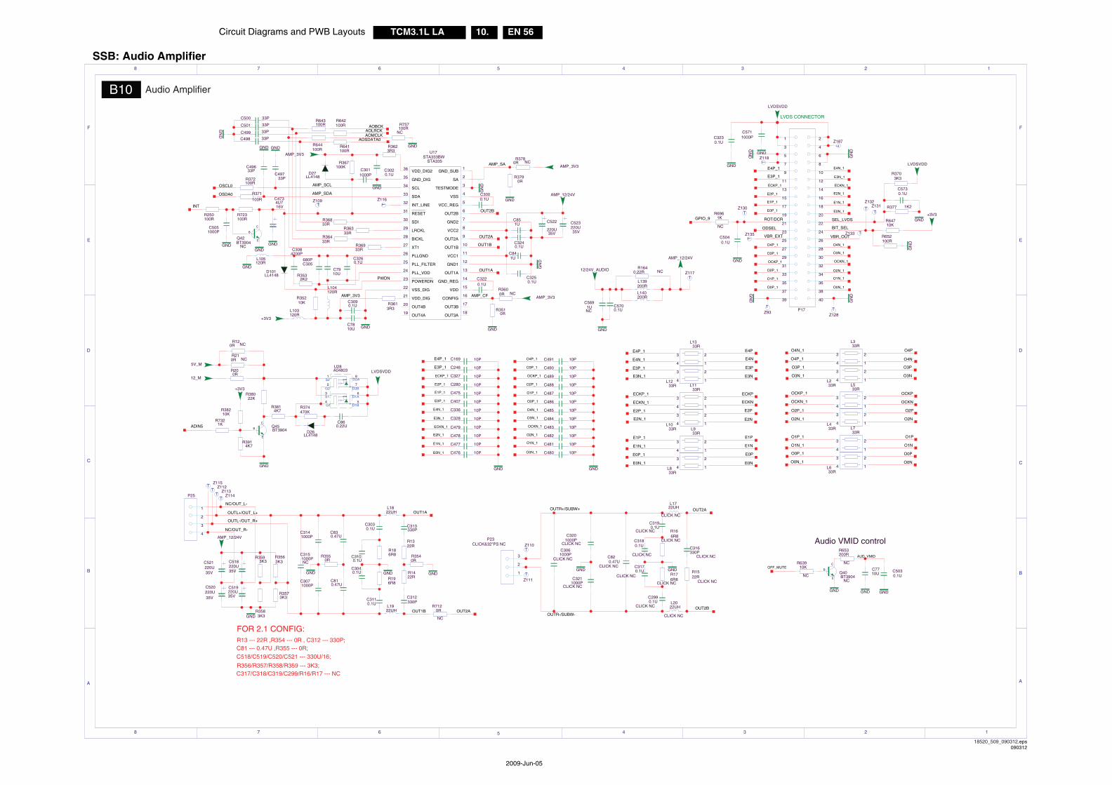
EN 56TCM3.1L LA 10.Circuit Diagrams and PWB Layouts
2009-Jun-05
SSB: Audio Amplifier
GND
T
T
TT
T
GND
GN
D
GNDGND GND
GNDGND
T
T
T
GND
GN
D
T
GND
GND
GN
D
GN
D
GND
GND
GN
D
GN
D
GN
D
T
T
GND
GND GND
GN
D
A
3 2 1
F
E
D
C
B
8 7 6 5
5
4 3 2 1
F
E
D
C
B
A
4678
GND
GND
T
TT
TT
GND
GND
GND
GND
GND
D2B
D2A
G1
G2
S1
D1B
D1A
S2
GNDGND
GND
T
GND
T
GND
VDD_DIG2
GND_DIG
SCL
SDA
INT_LINE
RESET
SDI
LRCKL
BICKL
XT1
PLLGND
PLL_FILTER
PLL_VDD
POWERDN
VSS_DIG
VDD_DIG
OUT4B
OUT3A
OUT3B
CONFIG
VDD
GND_REG
OUT1A
GND1
VCC1
OUT1B
OUT2A
VCC2
GND2
OUT2B
VCC_REG
VSS
TESTMODE
SA
GND_SUB
OUT4A
GND
LVDS CONNECTOR
FOR 2.1 CONFIG:R13 --- 22R ,R354 --- 0R , C312 --- 330P;C81 --- 0.47U ,R355 --- 0R;C518/C519/C520/C521 --- 330U/16;
R356/R357/R358/R359 --- 3K3;C317/C318/C319/C299/R16/R17 --- NC
Audio VMID control
3
4 1
2
L633R
3
4 1
2
L733R
3
4 1
2
L533R
3
4 1
2
L833R
3
4 1
2
L933R
3
4 1
2
L1033R
3
4 1
2
L1133R
3
4 1
2
L1233R
3
4 1
2
L1333R
100RR757
NC
100RR644
C520220U35V
C519220U35V
C518220U35V
C521220U35V
C523220U35V
LVDSVDD
B
C
E
Q45BT3904
R7321K
R38210K
R3914K7
E0N_1
NC/OUT_R-
C522
220U35V
1000PC315
NC
C5040.1U
R653200R
NCR63910K
NC
B
C
E
Q40BT3904
NC
36
35
34
33
32
31
30
29
28
27
26
25
24
23
22
21
20
18
17
16
15
14
13
12
11
10
9
8
7
6
5
4
3
2
1
19
U17STA333BW
STA335
R200R
R210R NC
R120R NC
R6961K
NC
1
10
11 12
13 14
15 16
17 18
19
2
20
21 22
23 24
25 26
27 28
29
3
30
31 32
33 34
35 36
37 38
39
4
40
5 6
7 8
9
P17
C480 10P
C481 10P
C482 10P
C483 10P
C484 10P
C485 10P
C486 10P
C487 10P
C488 10P
C489 10P
C490 10P
C491 10P
L2022UH
CLICK NC
C2990.1U
CLICK NC
C3170.1U
CLICK NC R176R8
CLICK NC
R1522R
CLICK NC
C316330P
CLICK NC
L1722UH
CLICK NC
0.1UC319
CLICK NC R166R8
CLICK NCC3180.1U
CLICK NC
1000PC321
CLICK NC
C820.47U
CLICK NC
C3201000P
CLICK NC
1000PC306
CLICK NC
1
2
3
P23CLICK&32"PS NC
R7120R
NC
R723100R
D101LL4148
PWDN
B
C
EQ42BT3904
NC
C3230.1U
R652100R
R64710K
R377 1K2
C5730.1U
R3703K3
ROT/DCR
Z130
1UC569
NC
3K3R358
R3573K3
3K3R356R359
3K3
NC/OUT_L-
C5700.1U
R1640.22R NC
120RL103
L140200R
200RL139
OUTR-/SUBW-
OUTR+/SUBW+OUTL+/OUT_L+
OUTL-/OUT_R+
1
2
3
4
P25
ODSEL
R3814K7
C860.22U
LVDSVDDC3011000P
C3020.1U
AMP_12/24V
AMP_12/24V
Z11712/24V_AUDIO
AMP_12/24V
C3084700P
D27LL4148
R367100K
C4734U716VINT
R250100R
C5051000P
GPIO_9
OSCL0
330PC312
0RR354
R1322R
C810.47U
R3550R
R3780R NC
7
8
4
2
3
5
6
1
A04803U28
0RR360
NC
22RR14
+3V3
ADIN5
R38022K
C851U
C841U
12_M
5V_M
L1922UH
L1822UH
0RR379
R371100R
OCKPECKP
O1N_1
O1P_1
E0N_1
C475 10P
C328 10P
C479 10P
C478 10P
E1N_1
C407 10P
E2P_1
R196R8
R35210K
LVDSVDD
VBR_OUTVBR_EXT
+3V3
C3090.1U
OSDA0
C169 10P
C246 10P
C327 10P
C280 10P
C830.47U
OUT2A
OUT2A
OUT1BOUT2B
Z115Z112
Z114Z113
Z118
C500 33P
R374470K
C3250.1U
C3240.1U
L105120R
+3V3
AMP_3V3
33PC501
C499 33P
33PC498
C49733P
33PC496 AMP_3V3
C3260.1U
R372100R
AMP_3V3
33RR369
33RR368
R643100R
R642100R
R641100R
Z128
Z116
R186R8
33RR364
33RR363
C3220.1U
C3141000P
C313330P
C3110.1U
C3100.1U
R3532K2
1000PC307
C305680P
C3040.1U
0.1UC303
C7910U
10UC78
R3510R
L104120R
C3000.1UZ109
Z93
D26LL4148
AMP_SAE4P_1
E3P_1
ECKP_1
O0P_1 O0N_1
O1N_1
O2N_1
OCKN_1
O3N_1
O4N_1
O1P_1
O2P_1
OCKP_1
O3P_1
O4P_1
E0N_1
E1N_1
E2N_1
ECKN_1
E3N_1
E4N_1
E0P_1
E1P_1
E2P_1
AOSDATA0AOMCLKAOLRCK
AOBCK
OUT1A
OUT1A
OUT2B
OUT1B
OUT2A
AMP_CF
AMP_SDA
AMP_SCL
Z111
Z110
E4P
E3P_1 E3P
E3N
E4NE4N_1
E3N_1
O0N_1 O0N
O0P_1 O0P
O1N
O1PO1P_1
O1N_1
O2N
O2P
ECKN
E2P
E2N
E1P
E1N
E0P
E0N
ECKN_1
E2P_1
E1P_1
E1N_1
OCKN
O2N_1
O2P_1
OCKN_1
OCKP_1
O4N_1
O4P_1
O3P_1
O3N_1 O3N
O3P
O4N
O4P
ECKP_1
E2N_1
E0P_1
E4P_1
O4P_1
O3P_1
OCKP_1
O2P_1
O0P_1
E4N_1
E3N_1
ECKN_1
E2N_1
E4P_1
ECKP_1
E1P_1
E0P_1
O0N_1
O3N_1
O4N_1
OCKN_1
O2N_1
E3P_1
C336 10P
C477 10P
C476 10P
C7710U 0.1U
C503
AUD_VMID
OFF_MUTE
C5711000P
Z187
BIT_SEL
SEL_LVDS
Z131Z132
Z133Z135
AMP_3V3
3R3R361
3R3R362
3
4 1
2
L433R
3
4 1
2
L233R
3
4 1
2
L333R
B10 Audio Amplifier
18520_509_090312.eps090312
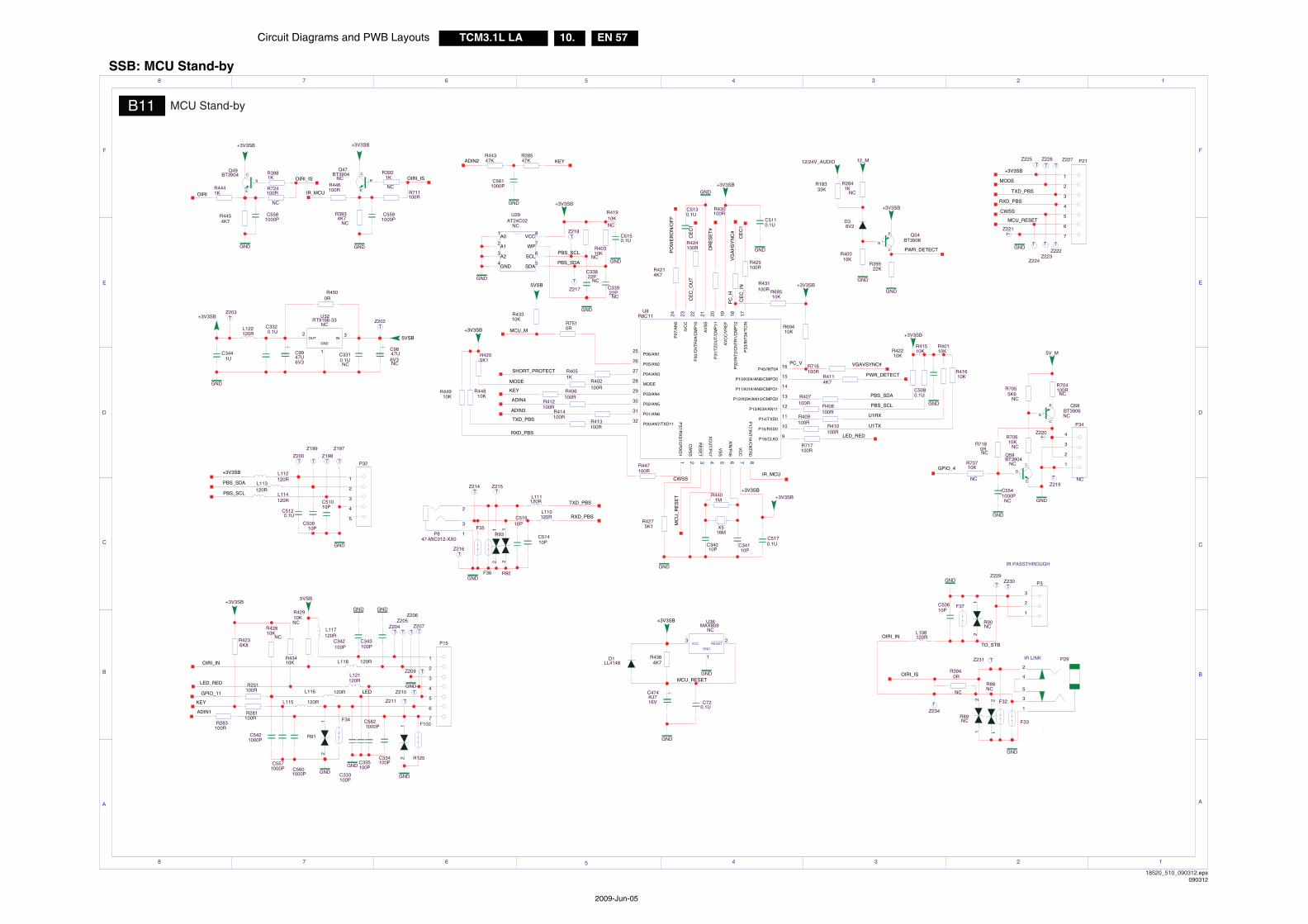
Circuit Diagrams and PWB Layouts EN 57TCM3.1L LA 10.
2009-Jun-05
SSB: MCU Stand-by
GND
GND
GND
T
GND
GND
GND
GND
GND
GND GND
GND
GND
GND
T
GND
T
T
GND
T T
GND
T
GND
GND
GND
GND
T
GND
SDA
SCL
WP
VCC
GND
A2
A1
A0
T
T
T T T
TTT
T
TTTT
TTTT
T
GND
RESETVCC
GND
GND
T
T
T
GND
GND
GND
GND
T
GND
T
INOUT
GND
P00/AN7/TXD11
P01/AN6
P02/AN5
P03/AN4
MODE
P04/AN3
P05/AN2
P06/AN1
P07
/AN
0
IVC
C
P30
/CN
TR
0#/C
MP
10
AV
SS
P31
/TZ
OU
T/C
MP
11
AV
CC
/VR
EF
P32
/INT
2/C
NT
R1/
CM
P12
P33
/INT
3#/T
CIN
P45/INT0#
P10/KI0#/AN8/CMPO0
P11/KI1#/AN9/CMPO1
P12/KI2#/AN10/CMPO2
P13/KI3#/AN11
P14/TXD0
P16/CLK0
P17/IN
T1#/C
NT
R0
VC
C
XIN
/P46
VS
S
XO
UT
/P47
RE
SE
T
CW
SS
P37/R
XD
10/RX
D1
P15/RXD0
A
3 2 1
F
E
D
C
B
8 7 6 5
5
4 3 2 1
F
E
D
C
B
A
4678
IR PASSTHROUGH
IR LINK
1
2
3
4
5
6
7
P21
1
2
3
P3
MCU_M
D38V2
R18333K
R40010K
C5821000P
C5601000P
100RR281
100RR283
1
3
5
2
4
P29
R2841K
NC
R7510R
RXD_PBS
R4236K8
R4214K7
32
31
30
29
28
27
26
25
24 23 22 21 20 19 18 17
16
15
14
13
12
11
9
87654321
10
U8R8C11
10KR433
MODE
SHORT_PROTECT
5VSB
1
2
3
4
5
P32
C51010P
C50910P
C5120.1U
L114120R
L113120R
L112120R
3
1
2
P847-MIC012-XX0 C514
10P
C51610P
12
R93
12
R92
R3940R
NC
21
R89NC
21
R88NC
C50610P
21
R90NC
L108120R
OIRI_IS
OIRI_IN
F37
R42810K
NC
R4441K
R40310K
NC
R41910KNC
R39922K
100RR251
C34110P
C34010P
X516M
R4275K1
C9847U6V3NC
C33822P
NC
C33922PNC
L121120R
L118 120R
L117120R
L116 120R
L115 120R
C9947U6V3
L111120R
L110120R
16V4U7C474
32
1
U32RT9166-33
NC
Z219
R70610K
NC
C5541000PNC
R70710K
NC
B
C
E
Q59BT3904
NC 1
2
3
4
P34
NC
B
E
C
Q58BT3906NC
R704100RNC
R7055K6
NC
C5611000P
R430100R
+3V3SB
TXD_PBS
1
2
3
4
5
6
7
P15
RXD_PBS
5VSB
Z202
R402100R
R4051K
R28547K
R44347K KEY
ADIN1
F34
21
R91
LED
Z209
Z210
Z211
C5421000P
C5571000P
KEY
C335100P
C5591000P
R446100R
C5581000P
IR_MCUR724100R
NC
R711100ROIRI
R3921K
NC
GPIO_11
LED_RED
OIRI_IN
R42910KNC
R69410K
0RR450
+3V3SB
+3V3SB
C720.1U
23
1
U36
NCMAX809
C3441U
C3310.1UNC
B
C
E
Q47BT3904
NC
4K7R393
NC
B
C
E
Q49BT3904
4K7R445
R3981K
OR
ES
ET
#
R43410K
MC
U_R
ES
ET
D1LL4148
MCU_RESET
F33
Z203
L122120R
C3320.1U
C5110.1U
C5130.1U
R424100R
R431100R
R425100R
R69510K
R44910K
R44810K
R4205K1
R406100R
R412100R
R414100R
R413100R
R447100R
R4401M
C5170.1U
R41610K
R40110K
C5080.1U
R41510KR422
10K
R716100R
R4114K7
R407100R
R408100R
R409100R
R410100R
R717100R
C334100P
C333100P
C342100P
C343100P
Z204Z205
Z206
Z207
Z200
Z199
Z198
Z197
Z221
Z224Z223
Z222
Z227Z226Z225
C5150.1U
Z218
Z217
5
6
7
8
4
3
2
1
U29AT24C02
NC
VGAVSYNC#
PWR_DETECT
TXD_PBS
F32
PWR_DETECT
U1TX
PBS_SCL
+3V3SB
VG
AH
SY
NC
#
5VSB
+3V3SB
PBS_SDA
ADIN2
LED_RED
GPIO_4
PBS_SDA
+3V3SB
Z215
IR_MCUCWSS
CE
C_O
UT
CE
C1
ADIN3
KEY
F35
+3V3SB
U1RX
R7180RNC
5V_M
CE
C1
Z214
+3V3SB
B
E
C
Q54BT3906
+3V3SB
12/24V_AUDIO 12_M
4K7R438
Z230Z229
OIRI_IS
TXD_PBS
+3V3SB
MODE
PBS_SDA
PBS_SCL
Z234
Z231
+3V3SB
Z220
+3V3SB+3V3SB
+3V3SB
+3V3SB
PO
WE
RO
N/O
FF
CE
C_I
N
ADIN4
PBS_SCL
Z216
MCU_RESET
CWSS
RXD_PBS
F36
PC
_H
PC_V
TO_STB
OIRI_IS
F100
21
R125
B11 MCU Stand-by
18520_510_090312.eps090312
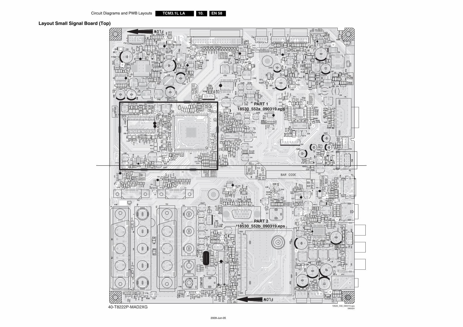
EN 58TCM3.1L LA 10.Circuit Diagrams and PWB Layouts
2009-Jun-05
Layout Small Signal Board (Top)
40-T8222P-MAD2XG 18520_556_090319.eps090324
PART 118530_552a_090319.eps
PART 218530_552b_090319.eps
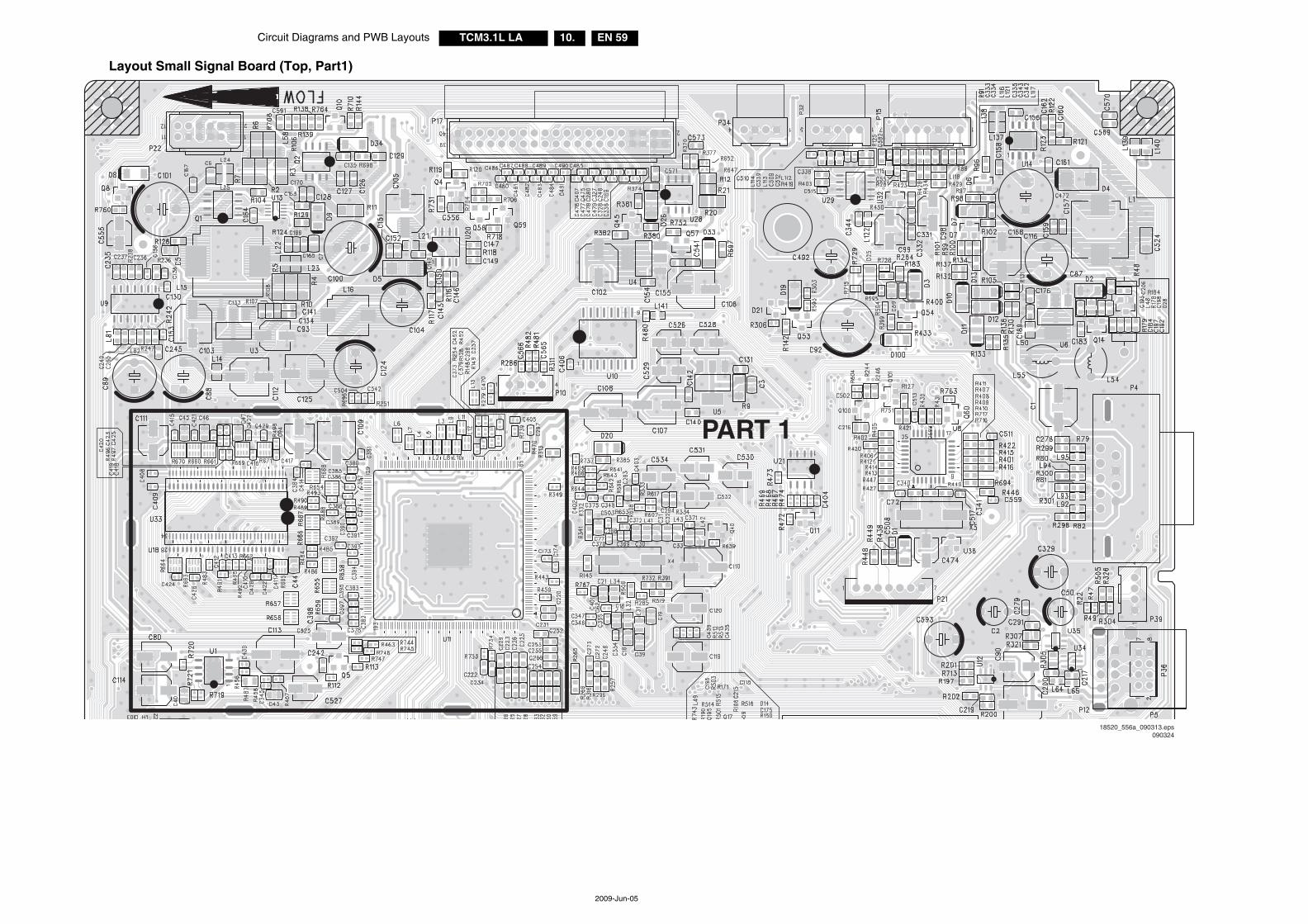
Circuit Diagrams and PWB Layouts EN 59TCM3.1L LA 10.
2009-Jun-05
Layout Small Signal Board (Top, Part1)
18520_556a_090313.eps090324
PART 1
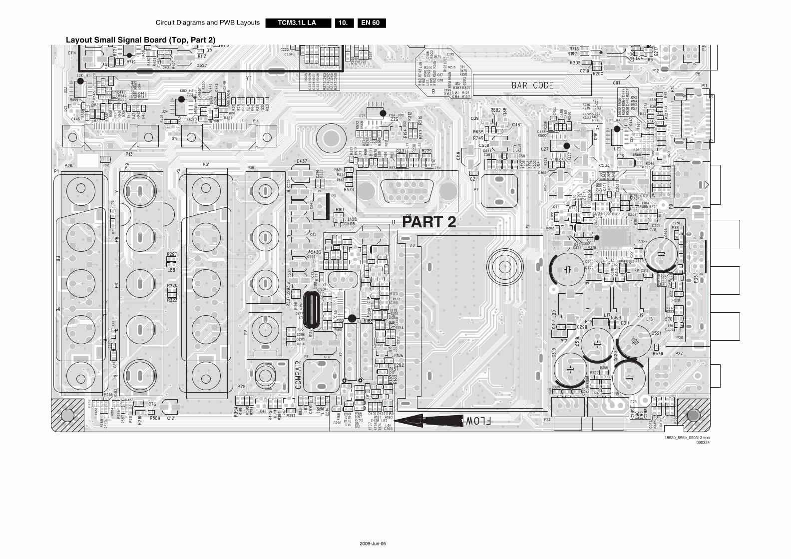
EN 60TCM3.1L LA 10.Circuit Diagrams and PWB Layouts
2009-Jun-05
Layout Small Signal Board (Top, Part 2)
18520_556b_090313.eps090324
PART 2
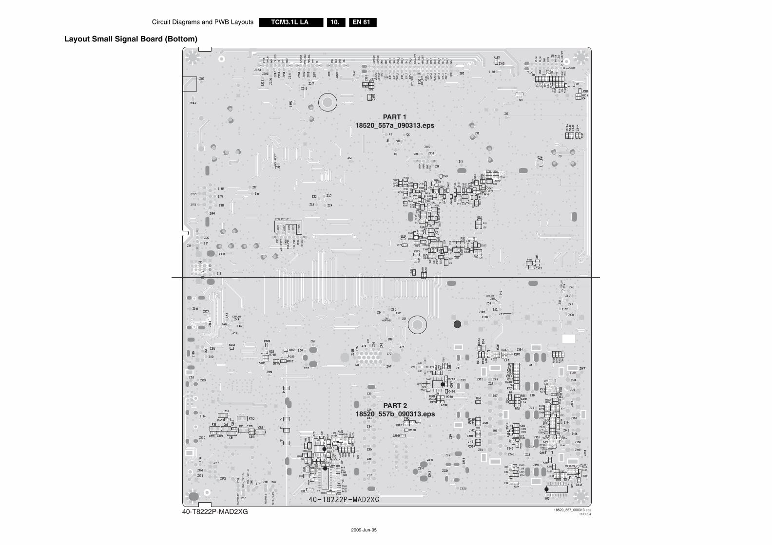
Circuit Diagrams and PWB Layouts EN 61TCM3.1L LA 10.
2009-Jun-05
Layout Small Signal Board (Bottom)
40-T8222P-MAD2XG 18520_557_090313.eps090324
PART 118520_557a_090313.eps
PART 218520_557b_090313.eps
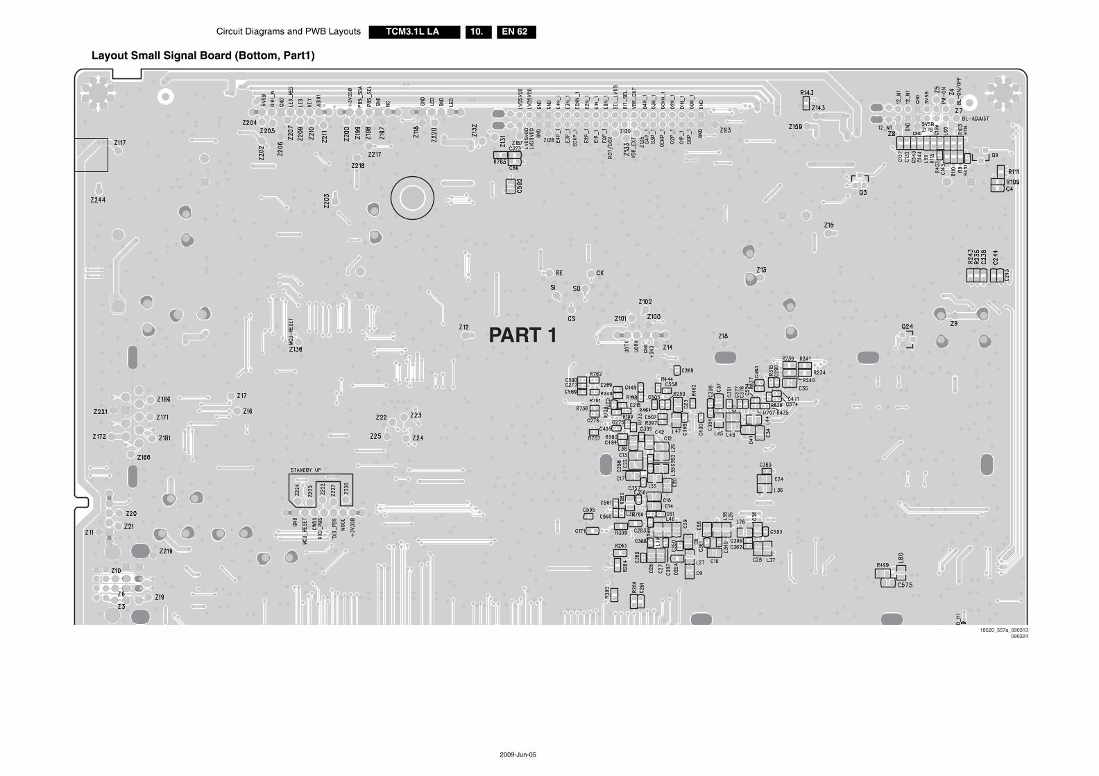
EN 62TCM3.1L LA 10.Circuit Diagrams and PWB Layouts
2009-Jun-05
Layout Small Signal Board (Bottom, Part1)
PART 1
18520_557a_090313090324
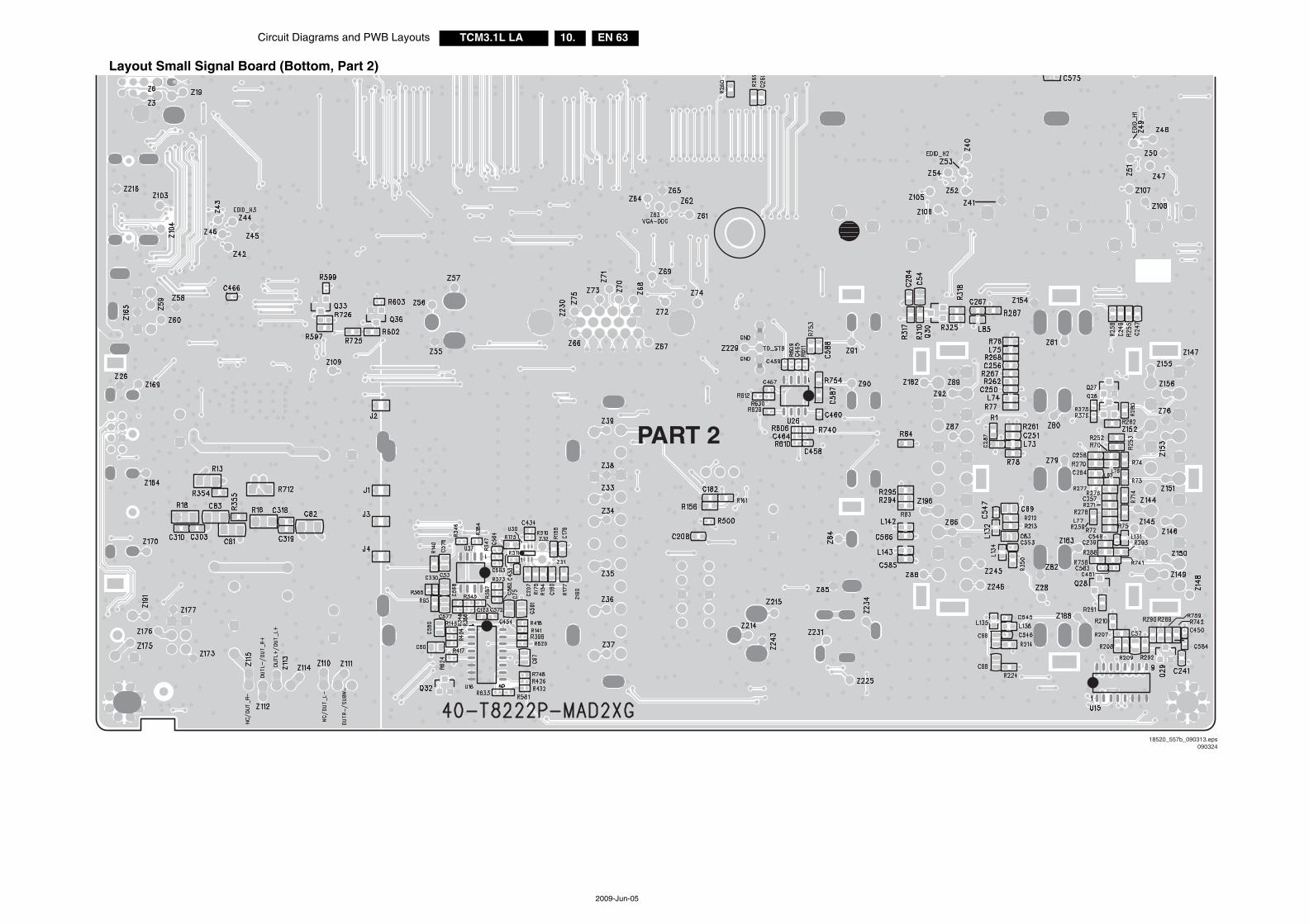
Circuit Diagrams and PWB Layouts EN 63TCM3.1L LA 10.
2009-Jun-05
Layout Small Signal Board (Bottom, Part 2)
18520_557b_090313.eps090324
PART 2
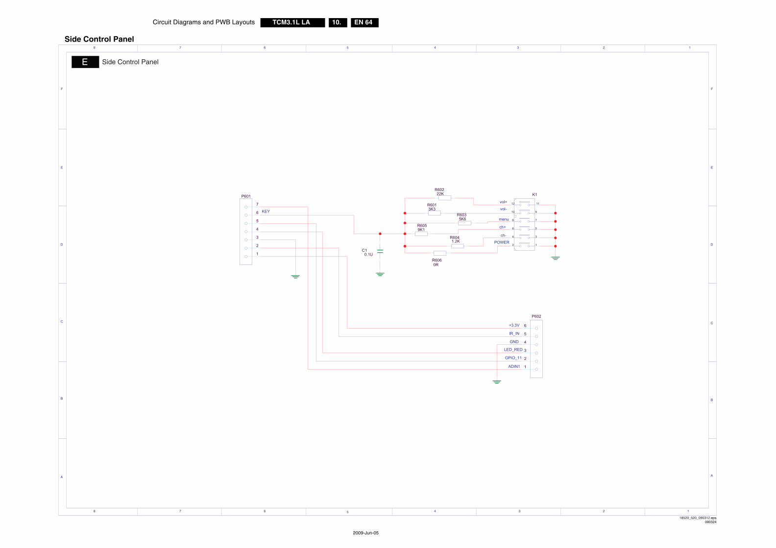
EN 64TCM3.1L LA 10.Circuit Diagrams and PWB Layouts
2009-Jun-05
Side Control Panel
A
3 2 1
F
E
D
C
B
8 7 6 5
5
4 3 2 1
F
E
D
C
B
A
4678
E Side Control Panel
KEY
GND
IR_IN
+3.3V
GPIO_11
LED_RED
ch+
ch-
menu
vol-
vol+
POWER
ADIN1
R6060R
R60222K
R6041.2K
R6013K3
1
2
3
4
5
6
P602
R6059K1
C10.1U
R6035K6
1
2
3
4
5
6
7
P601
3
5
7
9
12
4
6
8
10
12 11
K1
18520_520_090312.eps090324
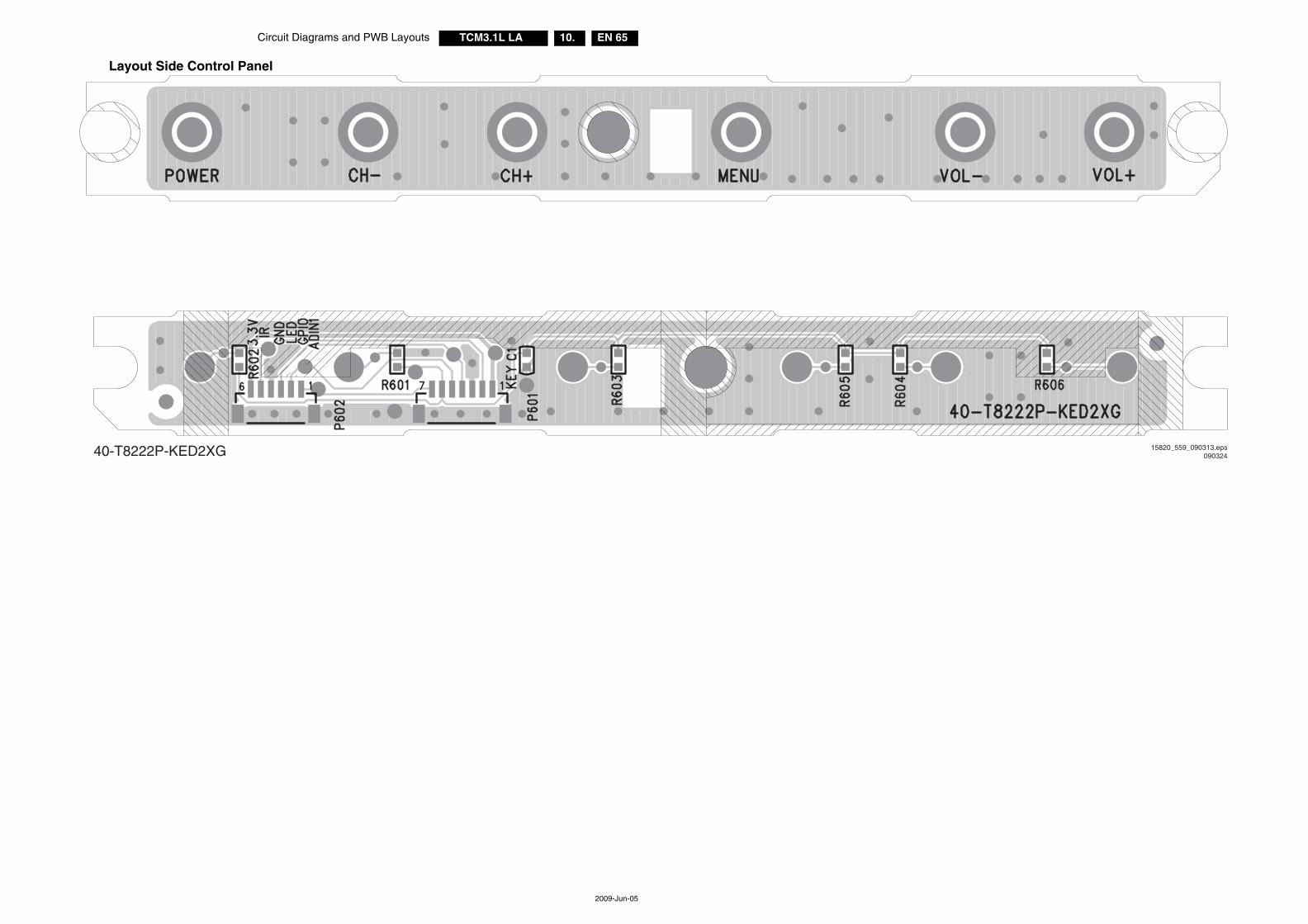
Circuit Diagrams and PWB Layouts EN 65TCM3.1L LA 10.
2009-Jun-05
Layout Side Control Panel
40-T8222P-KED2XG 15820_559_090313.eps090324
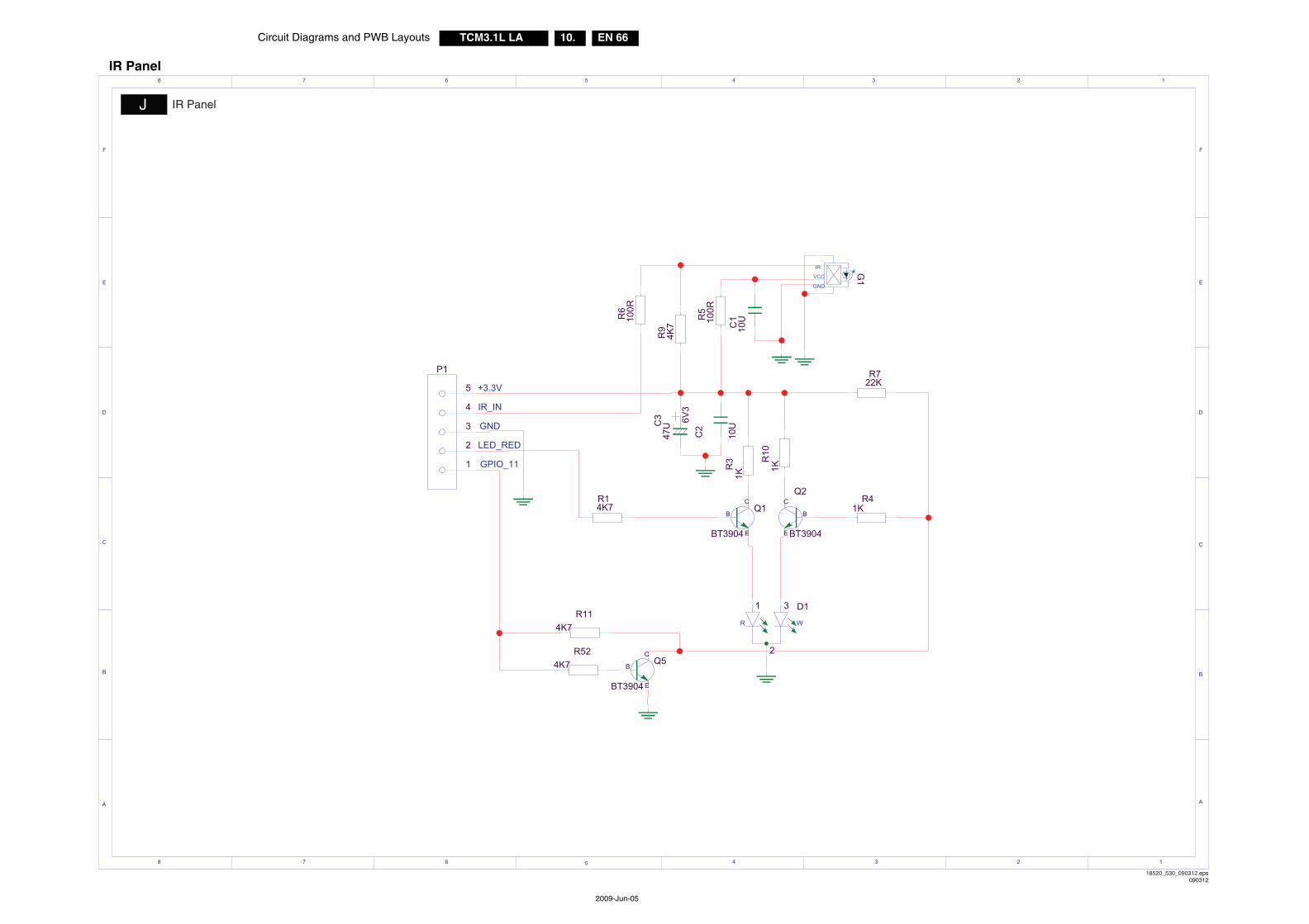
EN 66TCM3.1L LA 10.Circuit Diagrams and PWB Layouts
2009-Jun-05
IR Panel
A
3 2 1
F
E
D
C
B
8 7 6 5
5
4 3 2 1
F
E
D
C
B
A
4678
J IR Panel
VCC
IR
GND
R W
GND
IR_IN
+3.3V
LED_RED
GPIO_11
R524K7
2
1 3 D1
R41K
22KR7
B
C
E
Q2
BT3904
4K7R1
1KR
31
2
3
4
5
P1
E
C
B
BT3904
Q5
B
C
E
Q1
BT3904
G1
100R
R5
R9
4K7
R6
100R
6V3
47UC
3
10U
C2
C1
10U
1KR
10
R114K7
18520_530_090312.eps090312
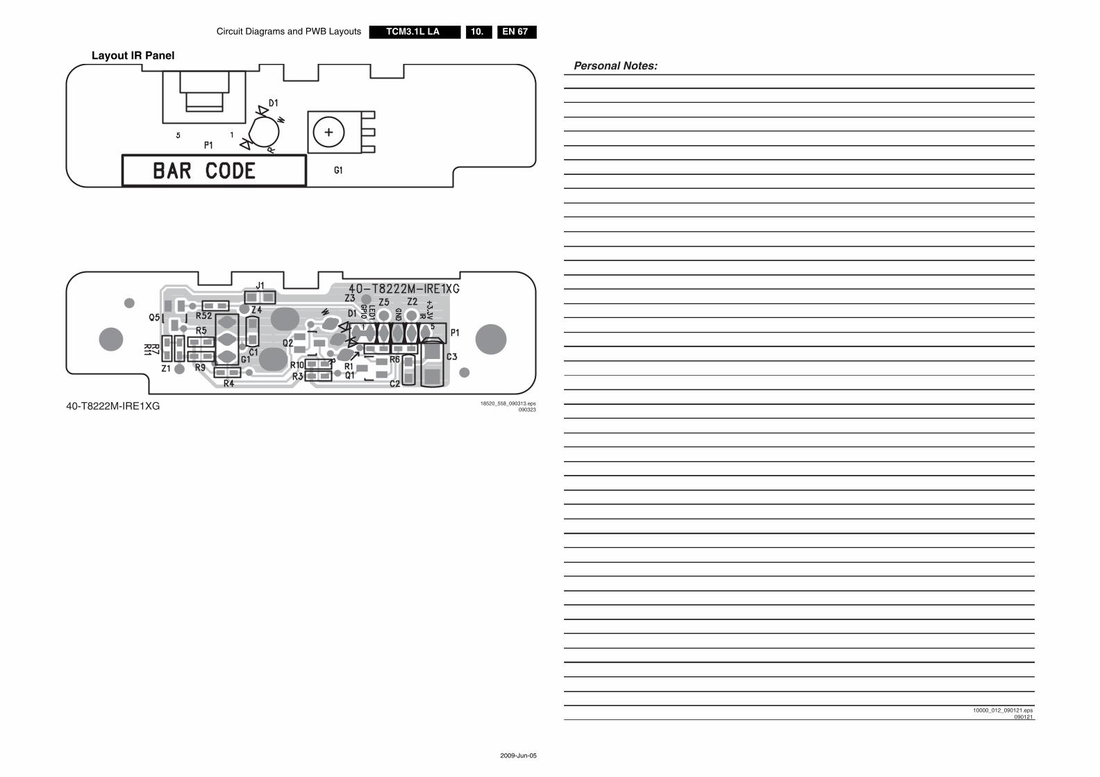
Circuit Diagrams and PWB Layouts EN 67TCM3.1L LA 10.
2009-Jun-05
Layout IR Panel
40-T8222M-IRE1XG 18520_558_090313.eps090323
Personal Notes:
10000_012_090121.eps090121


![Philips q548.1e La Chassis Lcd [ET]](https://img.dokumen.tips/doc/110x75/54a14f19ac7959027f8b4670/philips-q5481e-la-chassis-lcd-et.jpg)