Embed Size (px)
Citation preview

Comparison of Three Phase Current Source Inverters and Voltage Source Inverters Linked with DC to DC Boost Converters for Fuel Cell Generation Systems
Comparison of Three Phase Current Source Inverters and Voltage SourceInverters Linked with DC to DC Boost Converters for Fuel Cell Generation
Systems
Malte Mohr', Friedrich W. Fuchs2Christian-Albrechts-University of Kiel
Kaiserstr. 2, 24143 Kiel, GermanyTel.: +49 - 431 8806104 / Fax: +49 - 431 8806103
'mam(ktf.uni-kiel.de 2fwf(,tf.uni-kiel.de
KeywordsFuel cells system, Renewable energy systems, Current Source Inverter (CSI), Voltage Source Inverters(VSI), Distributed power, Design
AbstractThree phase current source inverters (CSI) and voltage source inverters linked with a dc to dc boostconverter (VSI+BC) are appropriate solutions to convert electrical energy for distributed fuel cellgeneration systems. The performance of CSI's and VSI+BC's in this application is shown and bothtopologies are compared to each other concerning their power semiconductor design rating and theirsemiconductor power losses.
I. IntroductionFuel cells can be an important component of future energy systems, enabling electricity and heatgeneration from hydrogen or similar substances with zero or nearly zero emission. Their introduction is inthe stage ofbeginning as their development has not yet been finished.
Fuel cells provide a variable dc current at variable fuel cell voltage. They have to be connected to the ac
mains by means of inverters. Because of the comparatively low voltage of a fuel cell stack for low andmedium power, the fuel cell voltage is usually lower than the line voltage, the inverter has to increase thevoltage when feeding into the mains [1].
Apart from the requirements of dc current control capability, adaption of the voltage level and operationwith high efficiency, the inverter has to draw a well smoothed dc current from the fuel cell for a highlifetime of the cell [2]. In addition, it has to deliver low current harmonics to the mains with respect to thestandards. Moreover, the inverter ideally provides a unity power factor in the mains, however, a variationof the power factor cos((p) from 0.95 to 1 for example is desirable.
The usual solution is a voltage source inverter in series with a dc/dc converter [3] [4]. The dc link voltageof the voltage source inverter has to be greater than the maximum value of the phase to phase voltage ofthe line. Up to a ratio between fuel cell voltage Vf, and the dc link voltage VIink of Vlinl/Vf, = 3 the boostconverter is an appropriate solution to achieve these requirements [4].
The current source inverter promises to be another interesting solution [5] [6]. The main advantage of thecurrent source inverter is that it increases the voltage towards the mains itself, so an additional dc/dcconverter may not be necessary. This results in less complexity of the system and its control. Apart from[6], investigations of the current source inverter connected to fuel cells have not been found in theliterature.
EPE 2005 DresdenP.1
FUCHS Friedrich-Wilhelm
EPE 2005 - Dresden ISBN: 90-75815-08-5 P.1

Comparison of Three Phase Current Source Inverters and Voltage Source Inverters Linked with DC to DC Boost Converters for Fuel Cell Generation Systems
In this paper, both converter systems, applied to a fuel cell and feeding into the mains, are compared byanalytical analysis concerning their semiconductor design rating and their semiconductor power losses. Inchapter II, the basic performance of the fuel cell and of both inverter systems is introduced. In chapter III,
the power losses of the power semiconductors are shown. Chapter IV shows the power semiconductordesign rating and its results. Chapter V shows the results of the power loss calculation. The two chapterslast mentioned include a comparison of the two systems. Chapter VI provides a short prospect of CSIswith reverse blocking IGBT and chapter VII presents the conclusion.
TI. Basic system performance
A Fuel cell characteristicsFigure 1 shows an example of the characteristic curve, fuel cell voltage Vf, vs. current density J, of a
single fuel cell [1]. Recommended operation of the cell is in the ohmic region (about a current density of0.2 to 1 A/cm2 in the curve below). On the one hand operation in the concentration region (decliningsection at about a current density of 1.1 to 1.2 A/cm2 in the characteristic curve) of the fuel cell yields to a
bad efficiency of the fuel cell and on the other hand it may damage the fuel cell and has to be avoided [2].
VfC [V];1,IV]
operating point
0 V at no load operating point at
0,8 - ~ nominal load
0,7~~~~~~~~~~~~~'
0ne- --- ---------------
0,4 - _
0,3 -
t PpR 0)2 0,4 016 ot8 1 1,'2 1,4
j [Acm'
Fig. 1: Example of a characteristic curve of a single fuel cell
The fuel cell voltage typically specified in fig. 1 refers to one single fuel cell with typical current density J.There are characteristic curves that show other or lower voltage at nominal load. The current, delivered bythe fuel cell, depends on its cell area, higher system voltages can be obtained by connecting several fuelcells in series (fuel cell stacks).
B Voltage source inverter linked with boost converterIf a voltage source inverter is used for mains feed in, the dc link voltage has to be greater than the rectifiedline to line voltage [7]. So the low level fuel cell dc voltage has to be increased towards the dc linkvoltage. This can be achieved by using an additional boost converter, the whole system is shown in fig. 2.The dc link capacitor decouples the voltage source inverter and the boost converter and keeps the dc linkvoltage ripple to an adequate level. A feasible power flow control method could be to keep the dc linkvoltage constant via the boost converter.
C Current source inverterThe current source inverter, whose topology is shown in fig. 3, increases the voltage towards the mains byitself, so the voltage of the fuel cell must be lower than the lowest rectified line to line voltage [5] if thefuel cell is directly connected to the CSI. At the CSI, similar to the VSI+BC system, the dc link inductorLd at the fuel cell side yields to an appropriate dc current ripple. The switches of the current source
inverter have to be reverse blocking. If IGBTs are used for the current source inverter, the reverse
EPE 2005 DresdenP.2
FUCHS Friedrich-Wilhelm
EPE 2005 - Dresden ISBN: 90-75815-08-5 P.2

Comparison of Three Phase Current Source Inverters and Voltage Source Inverters Linked with DC to DC Boost Converters for Fuel Cell Generation Systems
blocking capability can at present only be achieved with diodes connected in series to the IGBTs. Thisyields to relatively high semiconductor conduction losses. Another interesting semiconductor is thereverse blocking IGBT (RBIGBT). The development of RBIGBT is in progress [8] so it can be supposedthat they will be available in the foreseeable future also for the CSI.
Ld.
systemLl L
| | V2 I X @d iL12 L
It )~ -F':'--S " 'l''[ w w 1w l''
Fig. 2: Circuit diagram of a voltage source Fig. 3: Circuit diagram of a current source inverterinverter linked with a boost converter for a fuel for a fuel cell generation system.cell generation system.
III. Power Semiconductor power losses
A Semiconductor conduction and switching lossesAnalytical derivation of semiconductor losses for the current source inverter (CSI) and for the voltagesource inverter has been carried out in [9]. In the following the forward characteristics of thesemiconductors have been linearised [9]. So forward or conduction losses Pc of the semiconductors havebeen calculated using (1). VCEO and VFO constitute the IGBT's and diode's threshold voltages, rCE and rFconstitute their differential ohmic resistance.
PJGT = V iv + rC iv; PDiode V iv + r (1)
The switching losses depend on switching voltage and current. The switching loss energies Es of theIGBTs (EON, ,, EOFF, 1) and of the diodes (Erec) have been linearised according to (2). Here ESR is the ratedswitching loss energy given from the datasheet for a reference commutation voltage Vref and a referencecurrent Iref while Vv and Iv are the actual commutation voltage and current of the valve [9].
E E VV Iv (2)SSRV I()
ref refThe proposed modulation schemes used here are standard ones as Half Wave Symmetrical Modulation(HSM) for the CSI [10] and so called Suboptimal Space Vector Pulse Width Modulation (SVPWM) forthe VSI [9]. Sinusoidal line current and line voltages are assumed as well as a power factor of cos(p) = 1.In the following Vline is the line to line voltage of the line and iL is the line current. Vf, characterises thefuel cell or input dc voltage of the respective inverter, Idl is the input dc current of the inverter and Vd,denotes the dc link voltage of the voltage source inverter.
Equations (3) and (4) show the conducting losses for the current source inverter for one IGBT and one
diode, equations (5) and (6) show their switching losses [9].
PCJIGBT =- [dl (VCE,O)+ Id * ()] (3)
PCDiode = dl * (VF,O)+ Idl (rE)] (4)
PSCIGBT fs - (EONI + EOFF,I) i) ie (5)SJGBT 6;r ONJ OFJ IeI, V ef
EPE 2005 DresdenP.3
FUCHS Friedrich-Wilhelm
EPE 2005 - Dresden ISBN: 90-75815-08-5 P.3

Comparison of Three Phase Current Source Inverters and Voltage Source Inverters Linked with DC to DC Boost Converters for Fuel Cell Generation Systems
PsDiode 6r= rec Ir
J (6)
Equations (7) and (8) show the conducting losses, (9) and (10) the switching losses of the voltage source
inverter (VSI) for each semiconductor as derived in [9]. M is the modulation index of the voltage source
inverter; it describes the ratio between line to line voltage Viine and dc link voltage Vd,.
pCJGBT = VL() i+ cos()j+ +M cos()j (7)
Esl = VF L 4 co ( )) Lyco(4(3s))4 (8)
PS,IGBT 1S (EONI + EOFFI) Vdc (9)
S,Diode zErec) Vdc (10)
Ke ref-
Conducting losses for the boost converter (BC) can be easily derived as follows: depending on themodulation index of the boost converter (neglecting voltage sags due to losses)
a=TON VIC (11)
TS VdCthe IGBT VI (see also fig. 2) is turned on for the time TON. It carries the input current Idl. This yields to itsconduction losses
CJIGBT dl (VCEO + rCE .Idl)a (12)
The Diode V2 is conducting during TON-Ts or (1-a). It carries also Idl while it is turned on, so the diode'sconducting losses are
PC,Diode 1dl(VFO +rF Idl) (l-a); note: Id, d2
The commutaion voltage of the IGBT and the Diode is the dc link voltage Vd,. During their conductiontime, the semiconductors carry the current Id1 so the switching losses of IGBT and diode in the boostconverter are as described in (14) and (15).
PS,IGBT fsfS(EON + EOFF ) V (14)
'eli~V ej 'ejpBC -E 'f Vdc Idl (15)S,Diode rec SVf (1)
ref 7ref
Assuming that the inverter supplies constant power to the line at constant line voltage, it can be seen from(7) - (10) that VSI's semiconductor losses for constant dc link voltage, equal to a constant modulationindex, are constant. Losses for BC (12) - (15) and CSI (3) - (6) depend on their input dc voltage due to thefact that dc current increases at constant power at decreasing dc voltage. Thus the power losses andsimilarly the installed power of BC and CSI is increasing for decreasing voltages at a given constantpower.
IV. Power Semiconductor ratingA Definition of installed semiconductor power
Semiconductor costs for similar voltages and similar loss performance of the semiconductor are nearlylinear to their current carrying capability. To compare CSI and VSI+BC to each other concerning their
EPE 2005 DresdenP.4
FUCHS Friedrich-Wilhelm
EPE 2005 - Dresden ISBN: 90-75815-08-5 P.4
Comparison of Three Phase Current Source Inverters and Voltage Source Inverters Linked with DC to DC Boost Converters for Fuel Cell Generation Systems
required semiconductor power, an installed semiconductor power, here also called rated semiconductorpower has been established. It is defined as
PSC,IGBT = VCES IC (16)for the IGBTs with maximum dc collector current Ic and
PSC,Diode = VCES IF (17)for the diodes with maximum dc forward current IF and maximum blocking voltages VCES. Total ratedsemiconductor power for one inverter is here defined as the sum of the separate rated powers for allrequired semiconductors.
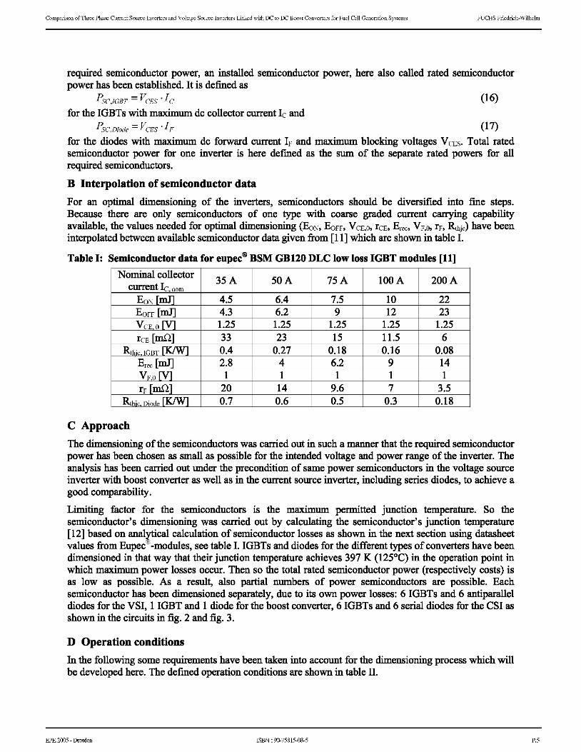
B Interpolation of semiconductor dataFor an optimal dimensioning of the inverters, semiconductors should be diversified into fine steps.Because there are only semiconductors of one type with coarse graded current carrying capabilityavailable, the values needed for optimal dimensioning (EON, EOFF, VCE,O, rCE, Erec, VF,O, rF, R1hj) have beeninterpolated between available semiconductor data given from [11 ] which are shown in table I.
Table I: Semiconductor data for eupec® BSM GB120 DLC low loss IGBT modules [11]Nominal collector 35A 50A 75A 100A 200A
currentIC nomEON [mJ] 4.5 6.4 7.5 10 22
EOFF [mJ] 4.3 6.2 9 12 23VCE, o [V] 1.25 1.25 1.25 1.25 1.25rCE [mM] 33 23 15 11.5 6
Rthic IGBT [K1W] 0.4 0.27 0.18 0.16 0.08Erec [mJ] 2.8 4 6.2 9 14VFO [V] 1 1 1 1 1rF [mQ] 20 14 9.6 7 3.5
Rthic, Diode [K/W] 0.7 0.6 0.5 0.3 0.18
C ApproachThe dimensioning of the semiconductors was carried out in such a manner that the required semiconductorpower has been chosen as small as possible for the intended voltage and power range of the inverter. Theanalysis has been carried out under the precondition of same power semiconductors in the voltage source
inverter with boost converter as well as in the current source inverter, including series diodes, to achieve a
good comparability.
Limiting factor for the semiconductors is the maximum permitted junction temperature. So thesemiconductor's dimensioning was carried out by calculating the semiconductor's junction temperature[12] based on analytical calculation of semiconductor losses as shown in the next section using datasheetvalues from Eupec`-modules, see table I. IGBTs and diodes for the different types of converters have beendimensioned in that way that their junction temperature achieves 397 K (1250C) in the operation point inwhich maximum power losses occur. Then so the total rated semiconductor power (respectively costs) isas low as possible. As a result, also partial numbers of power semiconductors are possible. Eachsemiconductor has been dimensioned separately, due to its own power losses: 6 IGBTs and 6 antiparalleldiodes for the VSI, 1 IGBT and 1 diode for the boost converter, 6 IGBTs and 6 serial diodes for the CSI asshown in the circuits in fig. 2 and fig. 3.
D Operation conditions
In the following some requirements have been taken into account for the dimensioning process which willbe developed here. The defined operation conditions are shown in table II.
EPE 2005 DresdenP.5
FUCHS Friedrich-Wilhelm
EPE 2005 - Dresden ISBN: 90-75815-08-5 P.5

Comparison of Three Phase Current Source Inverters and Voltage Source Inverters Linked with DC to DC Boost Converters for Fuel Cell Generation Systems
Table II: Defined operation conditionsFuel cell Nominal inverter power Mains line to line voltage Mains power factor
Vf, / J see fig. 1 Pinv= 27 kW Vline= 400 V +10% / - 15% Cos ((p) = 1
Due to the line voltage ofVie = 400 V the blocking voltage of the power semiconductors has been chosento VRSM = VCES = 1200 V for all semiconductors. This is not an optimal rating for both systems of thesemiconductor's blocking voltage. It has been done due to available semiconductors on the market.(Semiconductor's commutation voltage is different for both inverter topologies: at VSI and BC it is the dclink voltage Vd,, CSI's commutation voltage is the peak value of the line to line voltage Vhine.) A constantpower module case temperature of 363 K (90°C) was supposed, so only the thermal resistance Rthj,between junction and case has been taken into consideration.Some further constraints concerning operation at the mains have to be taken into consideration: accordingto standards, the fuel cell inverter system should operate at a mains voltage range of +10% / -15% fromnominal line voltage Vline. Moreover the aim is to keep the fuel cell at its operating point (constant current,constant voltage) during mains voltage fluctuations while the inverter system is operating. The chosencontrol method for the system VSI+BC is to keep the dc link voltage constant, so the VSI has tocompensate the mains voltage fluctuations while the BC adapts the fuel cell voltage fluctuations.For the VSI, the power semiconductor losses at constant power have their maximum at lowest mainsvoltage due to larger mains currents. Therefore, installed semiconductor power has to be estimated formaximum power at the lowest mains voltage. The dc link voltage has to be greater than rectifiedmaximum line to line voltage V, ioe 1. V .400 V [7]. Setting the dc link voltage to a maximumallowable value of Vjj{iax =750 V in respect of maximum capacitor voltages and semiconductor blockingvoltages, there is on the one hand an sufficient overshoot capability for inverter control and on the otherhand the input voltage range in combination with a boost converter is as wide as possible. This maximumvoltage should not be exceeded to avoid damage of semiconductors or dc link capacitors due toovervoltages for example.The CSI doesn't have a second decoupling energy storage like the dc link capacitor at the VSI+BCsystem. The mains voltage fluctuations as well as the fuel cell fluctuations will therefore be compensatedby the CSI, adjusting the modulation index. For the CSI, the power semiconductor losses at constantpower have their maximum at lowest dc input or fuel cell voltage due to a larger input current. Therefore,installed semiconductor power depends on input dc voltage and has to be estimated for maximum powerat the lowest impressed fuel cell voltage. For the current source inverter, there is a maximum allowedinput dc voltage it can work with. Assuming sinusoidal line currents, this voltage value is about
VCS]dc,max Vline (18)
and depends among other things on the mains power factor and the CSI filter design [5]. Considering thevoltage fluctuation and taking into account that there should be a supposed overshoot capability of about5% of the line to line voltage to control the dc current at lowest mains voltage, the maximum dc inputvoltage for the CSI is
vcYax = 0.85*095 400 V = 396V (19)
For an appropriate choice of filter elements, as shown in [5], the effect of filter components can hereby beneglected.Regarding the characteristic curve of a fuel cell (fig. 1), it becomes obvious that the input dc voltage rangeof an fuel cell inverter has to be from about 60 to 100 percent of the fuel cell no load voltage, assumingoperation over the entire power range. This results in an optimal fuel cell voltage from Vf, = 450...750 Vfor the VSI+BC and from Vf, = 238...396 V for the CSI (fuel cell voltage at nominal load and fuel cellvoltage at no load).
EPE 2005 DresdenP.6
FUCHS Friedrich-Wilhelm
EPE 2005 - Dresden ISBN: 90-75815-08-5 P.6

Comparison of Three Phase Current Source Inverters and Voltage Source Inverters Linked with DC to DC Boost Converters for Fuel Cell Generation Systems
E Installed / rated semiconductor powerThe standardised rated semiconductor power PsC, total / PINV has been calculated according to the concept as
shown in the previous section. Figure 4 illustrates the results. It shows the total rated semiconductor powerof VSI, BC, CSI and VSI+BC which are rated for different minimum dc input voltages Vf1, min at constantpower PINV 27 kW based on table III.
100
---___ CSI (red dashed line)80 optimal VSI+BC (black solid line)
(entire fuel cell load range) VSI (green chain dotted line)
% ..........lll__=======BC (blue dotted line)60 - optimal rating for VSI
(entire fuel cell load range)X 40 _lSi)~~~~~~~X
w 20 -
100 200 238 3O 400 450 500 600 700
minimum inverter dc input voltage Vf0, min
Fig. 4: Rated semiconductor power PSC. total /PINV ofBC+VSI and CSI. Operating conditions see table II.
The VSI+BC can be operated in the range below its highest dc voltage of Vdc, max = 750 V. Its ratedsemiconductor power is low and rises moderately with lower minimum inverter dc input voltage. Theconstant VSI semiconductor power is a result of its constant dc link voltage. The BC's semiconductorpower rises with lower minimum dc input voltage according to the voltage boost function and highersemiconductor current (see eq. (13)); Idl gets higher while Id2 is constant due to constant power PINV andconstant dc link voltage Vd,.The CSI can be operated at dc voltages Vfi lower than 396 V (at Viine= 0.85 400 V). With high "mini-mum dc inverter voltage", it shows low rated semiconductor power. When reducing the minimum dc inputvoltage of the CSI, the semiconductor power which has to be installed, rises significantly. This is due tothe fact that lower voltages cause higher currents at constant power and in addition the boost function ofthe CSI, equal to input short circuit, is done with four power semiconductors in series (see fig. 3).
For fuel cell application the "minimum dc input voltage" can be taken as the fuel cell voltage at itsoperating point at nominal load as shown in fig. 1 (high current at low voltage). Assuming the voltagerange shown in chapter IV, section D, there are optimal ratings for the two inverters for operation over theentire load range. The CSI then has to be rated for a fuel cell nominal load input voltage of 238 V (max.voltage 396 V), the VSI+BC has its fuel cell nominal load voltage at 450 V (max. voltage 750 V). Theresulting optimal rating of both inverters for the entire voltage range of the fuel cell is shown in fig. 4showing small to high advantages for the VSI+BC. For a given fuel cell stack the inverter's input voltageis given by the nominal voltage of the stack. For an nominal voltage of Vfi, min= 200 V for example, therated semiconductor power of the CSI is about 1.6 times larger than the VSI+BC's rated semiconductorpower. Limiting the voltage range for the current source inverter yields to less rated semiconductor powerwhich is shown in [4]. The CSI needs lower total rated semiconductor power for a narrow input voltagerange at input dc voltages near to its maximum input voltage value of VDC, max = 396 V. Extending thevoltage range or applying fuel cells with lower voltage leads to an even higher dimensioning of the CSIcompared to the VSI+BC.
EPE 2005 DresdenP.7
FUCHS Friedrich-Wilhelm
EPE 2005 - Dresden ISBN: 90-75815-08-5 P.7

Comparison of Three Phase Current Source Inverters and Voltage Source Inverters Linked with DC to DC Boost Converters for Fuel Cell Generation Systems
Table III gives the detailed analysis of the rated semiconductor power. It can be seen that for the CSI thecontent of diode's rated semiconductor power is only a little greater than IGBT's rated semiconductorpower. It has to be mentioned, that the semiconductor rating for the diodes especially in the CSI isaffected due to the comparative high thermal resistances Rthj,, Diode of the diodes. For the VSI maincontribution comes from the IGBT (9.4 compared to 4 for the diode).
Table III: Standardised rated semiconductor power for BC+VSI and CSI components (operationconditions see tab. II)
Inverter BC VSI BC+VSI CSI CSIType: IGBT diode IGBT diode IGBT diode overall IGBT diode overalllowest pBBC BpC S BC+VSC BC+VSI pBC+S p CS]input SCGBTrSC.Diode PSj1gfBT pSC.Diode SC,IGBT SC Diode SCSC'Dok;/ Cs] ,,Diod e
voltage inv inv inv inv inv inv iNVSlnNn iinVv100 V 14.5 8.9 9.4 4 23.9 12.9 36.8 40 53.4 93.4200 V 7.8 5.6 9.4 4 17.2 9.6 26.8 18.7 24.0 42.7300 V 5.1 4.5 9.4 4 14.5 8.5 23.0 13.4 16 29.4400 V 3.1 4 9.4 4 12.5 8.0 20.5 9.4 10.7 20.1500 V 2.2 3.6 9.4 4 11.6 7.6 19.2 - - -
600 V 1.6 3.3 9.4 4 11.0 7.3 18.3700 V 1.3 3.3 9.4 4 10.7 7.3 18.0
From table III and fig. 4 a fact becomes obvious: the VSI+BC needs remarkably less total ratedsemiconductor power in fuel cell application (about 1.8 times less than in the example shown at optimalrating for the inverter) and is therefore the favourable system. For fuel cells with lower nominal voltagethan shown in fig. 1 this effect increases. The reason is obvious: the step up or boost function to increasethe low fuel cell voltage to the mains voltage level is done in the VSI+BC by one power semiconductorconductiong at a time, IGBT or diode. For the CSI four power semiconductors, two IGBT and two diodescarry the high fuel cell current and have to be dimensioned according to the high fuel cell current.
Here, in general semiconductor power of IGBTs and diodes have been weighted equally. When regardingthe results with lower weighting for the diodes because of their lower costs, the CSI would appear more
favourable, but still worse than the VSI+BC.
V. Semiconductor lossesA Losses depending on input dc voltage and line current
In the following, semiconductor switching losses and conducting losses for the VSI and the CSI are
calculated as described above. As mentioned before, semiconductor losses of the CSI and VSI+BC forlower input dc voltages are relatively high. For a given inverter system, power losses decrease at risinginput dc voltages.
B Losses including fuel cell characteristic curve
As a result of increasing efficiency at higher input dc voltages and lower dc input currents it is of interestto take a closer look at semiconductor losses at partial fuel cell loads due to the fact that fuel cell voltagesincrease at lower fuel cell currents.
To compare losses of CSI and VSI+BC for operation at fuel cells the fuel cell characteristic curve, givenin fig. 1, has been taken into consideration. In the following, CSI and VSI+BC of differentdimensioning/rating for different minimum voltages as described in the section before have beencompared. At the nominal respectively minimal fuel cell/converter input voltage level their rated powerhas been chosen to Pmax = 27 kW. The fuel cell stack has been dimensioned and modelled in that way that
EPE 2005 DresdenP.8
FUCHS Friedrich-Wilhelm
EPE 2005 - Dresden ISBN: 90-75815-08-5 P.8

Comparison of Three Phase Current Source Inverters and Voltage Source Inverters Linked with DC to DC Boost Converters for Fuel Cell Generation Systems
its current level has been adapted by scaling the cell area, stack voltage has been achieved by connectingfuel cells in series, using data given from the characteristic curve (fig. 1).
Figure 5 shows power losses of different but adequate rated inverters of both topologies, connected to thefuel cell. Higher fuel cell stack voltage yields to lower fuel cell current and therefore decreasing power as
can be seen from the characteristic curve of a fuel cell (fig. 1). It can be seen that in general the CSI causes
greater losses at its nominal load at minimum input voltage compared to an VSI+BC. This correspondes tothe necessarily higher installed and fully exploited semiconductor power (fig. 4) of the CSI. In the partialload range at higher fuel cell voltages CSI's semiconductor losses reach the VSI+BC losses. In a mediumvoltage range at about 300 to 396 V CSI's semiconductor losses fall minor below VSI+BC losses. Butnote that the CSI is overdimensioned concerning power semiconductors (see chapter IV) and that thevoltage range of the CSI is limited due to its maximum permitted input dc voltage. At higher voltages theVSI+BC shows lower total losses due to decreasing losses in the boost converter.
3000 -_
2500 CSI: thick red line
_____VSI ±B : thin black line2000-
050
50
100 200 300 400 500 600 700 800
fuel cell voltage Vfr
Fig. 5: Semiconductor power losses of VSI+BC and CSI connected to fuel cell stacks (operatingconditions see tab. II; nominal fuel cell voltage Vfc, nom= 100, 200, 300, 400, 500, 600, 700 V; fuel cellcurve from fig. I)
VI. Future prospects
A Reverse blocking IGBTs for the current source inverterIn the context of matrix converter research the development of reverse blocking IGBTs (RBIGBT) is inprogress [8]. These devices could also be used in a current source inverter. Due to the lack of separateseries diodes the conducting losses of the CSI could be reduced.
For matrix converter operation it is shown in [8] that a reduction of approximately 20 % of totalsemiconductor losses can be achieved by using RBIGBT compared to conventional IGBTs and diodes inseries at a switching frequency of 15 kHz. Due to high switching losses of RBIGBT compared toconventional IGBT with series diode [8], a total semiconductor loss reduction of about 40 % can beestimated for a switching frequency of 3 kHz.
Relating to the the CSI this estimation shows that RBIGBT would significantly improve CSI's efficiencyand rated power in the fuel cell application because of the abolition of conducting losses in the seriesdiodes.
EPE 2005 DresdenP.9
FUCHS Friedrich-Wilhelm
EPE 2005 - Dresden ISBN: 90-75815-08-5 P.9

Comparison of Three Phase Current Source Inverters and Voltage Source Inverters Linked with DC to DC Boost Converters for Fuel Cell Generation Systems
VII. ConclusionTwo topologies of converters, the voltage source inverter linked with boost converter (VSJ+BC) and thecurrent source inverter (CSI) can be applied for the power feed in from fuel cells to the three phase mains.Both converters have been analyzed and compared to each other with regard to power semiconductordesign rating and power losses when feeding in power from fuel cells to the mains. The analysis has beendone by analytical calculation in steady state by average models. The comparison is based on a systemwith a power of 27 kW at a line to line voltage of 400 V, with fuel cell stacks of different nominalvoltages. Nevertheless, the results should be valid in a great power range. The converter is equipped withpower semiconductors designed to the fuel cell power.The analysis shows that for this application, the CSI always has to be equipped with a remarkably higherinstalled semiconductor power, compared to the VSI+BC. This is due to the fact that a high voltage rangehas to be covered and the CSI needs four power semiconductors to carry out the boost function at low fuelcell nominal voltage with high dc current. The boost converter in the VSI+BC system needs only one
power semiconductor which carries the current during boost operation. This yields necessarily to a muchhigher installed semiconductor power in the CSI.The comparison of the losses for both systems shows moderate to high advantages for the VSI, mainly forfuel cells with low nominal voltage and for operation in the full fuel cell voltage range. Evaluating this,one has to keep in mind that the CSI's power semiconductors are necessarily higher dimensionedcompared to the VSI.Finally it can be concluded that under the given circumstances and available IGBTs, regarding power
semiconductor design rating and losses, there is no need today to use CSIs to connect fuel cells to themains in spite of the CSI's interesting inherent voltage boost function. For fuel cells or other powersources with a more stiff dc link voltage the result would be more positive for the CSI in this application.Future reverse blocking IGBTs could moreover modify the result of this evaluation if RBIGBT showremarkable lower power losses than IGBTs with diodes in series.
References[1] Ledjeff-Hey, K. et. al.: Brennstoffzellen: Entwicklung, Technologie, Anwendung, edition 2, 2001, Muller
Verlag, Heidelberg[2] Gemmen, R.: Analysis for the effect of inverter ripple current on fuel cell operating condition; Journal of
fluids engineering, Vol.125 (2003), 3, pp. 576-585[3] Yaosuo X.; Liuchen C.; Kjaer, S.-B.; Bordonau, J.; Shimizu, T.: Topologies of single-phase inverters for small
distributed power generators: an overview, IEEE-Trans.-on-Power-Electronics; 2004; 19(5): 1305-1314[4] Solmecke, H.: Optimierte Stromrichter fir Brennstoffzellenanlagen (Optimized power converter for fuel cell
plants), phd-thesis, 1998, Fernuniversitat-Gesamthochschule Hagen; in German[5] Mohr, M.; Bierhoffg M.H.; Fuchs, F.W.: Dimensioning of a Current Source Inverter for the Feed-in of
Electrical Energy from Fuel Cells to the Mains, Proceedings of the Nordic Workshop on Power and IndustrialElectronics NORPIE 2004, Trondheim
[6] Rivas, C.; Rufer, A.: P.W.M. Current converter for electric energy production system from fuel-cells,Proceedings of the European Conference on Power Electronics and Applications EPE 2001, Graz
[7] Kazmierkowski, M. P.; Krishnan, R.; Blaabjerg, F.: Control in Power Electronics, Selected Problems; 2002;Academic Press, London
[8] Naito, T.; Takei, M. ; Nemoto, M.; Hayashi, T.; Ueno, K.: 1200 V Reverse Blocking IGBT with low loss forMatrix Converter, Proc. of Int. Symposium on Power Semiconductor Devices & ICs 2004, Kitakyushu
[9] Bierhoff, M.H.; Fuchs, F.W.: Power Semiconductor Losses in Voltage Source and Current Source IGBTConverters based on Complete Analytical Derivation, Proceedings of the PESC 2004, Aachen
[10] Halkosaari, T.; Tuusa, H.: Optimal Vector Modulation of a PWM Current Source Converter According toMinimal Switching Losses; Proceedings of the International Power Electronics Conference IPEC 2000, Tokyo
[11] datasheets of Eupec1 BSM GB12ODLC IGBT-Modules, 2004, Warstein[12] Konrad, S: Ein Beitrag zur Auslegung und Integration spannungsgespeister IGBT-Wechselrichter (A
contribution for the dimensioning and integration of voltage source IGBT inverters); phd-thesis; 1997, ISLE-Verlag, Ilmenau; in German
EPE 2005 DresdenP.10
FUCHS Friedrich-Wilhelm
EPE 2005 - Dresden ISBN: 90-75815-08-5 P.10