Embed Size (px)
Citation preview
Making Visible the Thermal Behaviour of Embedded Microprocessors on FPGAs. A Progress Report
Sergio Lopez-Buedo and Eduardo Boemo Computer Engineering Department
School of Engineering Universidad Autonoma de Madrid, Spain
{sergio.lopez-buedo, eduardo.boemo}@uam.es
ABSTRACT This paper shows a method to verifying the thermal status of complex FPGA-based circuits like microprocessors. Thus, the designer can evaluate if a particular block is working beyond specifications. The idea is to extract the output frequencies of an array of ring-oscillators previously distributed in the die, taking full advantage of the configuration port capabilities in Xilinx technology. As a result, it is shown that the FPGA technology offers the designers of embedded systems the possibility of viewing a detailed thermal map of a circuit at a minimum cost. The verification can be done in actual working conditions; for example with heat sinks and fans attached to the chip, inside the system case, or even in an on-board satellite application. The main results of the work are unthinkable using other alternatives like IR cameras, external sensors, or embedded diodes.
Categories and Subject Descriptors B.8.1 [Hardware]: Performance and Reliability – reliability, testing. B.6.1 [Hardware]: Logic design – logic arrays. C.3 [Computer Systems Organization]: Special-Purpose and Application-Based Systems – embedded systems
General Terms Measurement, Design, Reliability, Verification
Keywords FPGA, Embedded Processors, Temperature Measurement, Ring-Oscillator, Run-Time Reconfiguration, JBits.
1. INTRODUCTION Even considering that the quantitative effects of heat on electronic systems needs a carefully revision, it is accepted that high temperature and especially thermal gradients or stresses reduces both reliability and chip life [4]. In the FPGA arena, current technologies limit maximum temperature to 125 centigrade degrees. For an actual application,
the verification of this restriction is not an easy task. The designer should take into account aspects like the peak power, the effect of heat sinks and fans, board position, room temperature, or the influence of hot devices situated near the chip. The well-known formula:
DJAAJ PTT θ+= [1]
Is appropriated to characterize a chip packaging [1][9], but is a coarse model for any practical application. Current solutions, like the embedded diode available in Xilinx Virtex and Altera Statrix FPGAs, or the use of infrared cameras only solve partially the problem. In the first option, the temperature is measured in only one point of the die, so this information is only useful to know that there is a problem, but not to identifying it. On the other hand, infrared cameras require the direct vision of the silicon, and thus, they can not be employed in actual working conditions. The technique to verify die temperature proposed in this paper makes a novel use of the well-known readback and configuration port capabilities present in Xilinx FPGAs. The idea is simple but effective. The actual configuration, for example an embedded processor, is mixed with an array of ring-oscillators and counters. The output frequency of each ring is a function of the die temperature, which it is captured with an associated counter. New logic to operate these circuits is not required, as the measurement can be started by a simple reconfiguration of a LUT. Moreover, it is not necessary to use any new resources or dedicated I/O pads to read the temperature: the value in the counters can be obtained via readback, through the configuration port. The method is also compatible with dynamic reconfiguration, as the sensor (ring oscillator plus its associated counters) could be on-the-fly inserted. Two scenarios are possible: a full reconfiguration, where two hardware contexts are used: First, the application to be tested; and second, the array of sensors. At any moment, the main application can be stopped and a new bitstream with the second configuration can be loaded and activated. Then, the output frequencies are read back and the original bitstream is reloaded. For the smaller devices, the test can take only few milliseconds, a time much lower than the thermal constants of the system (the dominant constant has been measured to be around 150 ms [5]). The other alternative is to use run-time reconfiguration, where the sensors are dynamically inserted in the circuit when they are needed. As they are completely stand-alone (their only interface to the rest of the FPGA is the clock node), and all its operation is performed via the configuration port, these circuits are very suitable to be used with run time reconfiguration.
Permission to make digital or hard copies of all or part of this work for personal or classroom use is granted without fee provided that copies are not made or distributed for profit or commercial advantage and that copies bear this notice and the full citation on the first page. To copy otherwise, or republish, to post on servers or to redistribute to lists, requires prior specific permission and/or a fee. FPGA’04, February 22–24, 2004, Monterey, California, USA Copyright 2004 ACM 1-58113-829-6/04/0002…$5.00.
79
This possibility was also explored in this paper, by using JBits [2]. In any case, the main advantages of the technique proposed in this paper are that it uses a minimum chip area, no I/O pins, and the sensors can be placed in any point of the chip. They can be remotely operated, being suitable for application that requires high reliability like avionics or on-board satellite circuits. Detailed information of the thermal response and calibration techniques of the sensors has been presented in two previous works [6][7]. In this paper, the experiments are extended to demonstrate that the technique is sensitive enough to make visible points of high activity and temperature gradients in complex circuits like FPGA-embedded microprocessors. In the next section, the main alternatives to create an array of sensor are analyzed. After that, the features of the circuit to be tested, composed of two twin MIPS-I compatible processors, is summarized. Finally, main experimental results are shown in section 4.
2. AN ARRAY OF SENSORS In the experiments, an array of 4 by 8 sensors was placed in the FPGA. Two alternatives where explored to design these sensors. First, a sensor compatible with run-time reconfiguration was implemented using JBits. This technology was also utilized to control the circuits and readback the results. Being designed the sensor as an RTPCore (run-time parameterizable core using the CoreTemplate API) the array can be constructed by simply instantiating a sensor as many times as necessary: for (i=0; i<numOfSensors; i++) { sensor[i] = new TemperatureSensor("Sensor", clk); } for (i=0; i<numOfSensors; i++) { sensorOffset[i] = sensor[i].getRelativeOffset(); sensorOffset[i].setHorOffset(Gran.CLB, sensorXPos[i]); sensorOffset[i].setVerOffset(Gran.CLB, sensorYPos[i]); } for (i=0; i<numOfSensors; i++) { sensor[i].implement(TimeEnable,RingEnable,CountEnable); } Bitstream.connect(clk);
Each sensor makes use of 8 by 2 CLBs. Details about its design can be found in [5][6]. The space among them for the selected FPGA (XCV800) is 8 CLBs in the vertical direction and 7 CLBs in the horizontal one. The other alternative to implement the temperature sensors is to use a physical macro. It allows the designer to create a circuit equivalent to the JBits one, but using the conventional tools. The possibility of adding or eliminating the sensor at run-time operation is lost, but the sensor still can be controlled using partial reconfiguration, and accessed via readback. Thus, the array of sensors can be managed through the configuration port, without using additional pins. Other advantage of macros is the control of the placement and routing, two important parameters to simplify the calibration. It is also easy to create an array of sensors in this case, because the macro can be instantiated from VHDL: s00 : TempSensor port map (clk => buf_clk_sens); s01 : TempSensor port map (clk => buf_clk_sens); ...
Finally, since the macro is equivalent to the original sensor, the previous JBits code can be used to control and readback it. An important point to keep in mind is to use of the absolute location directive (LOC) to fix the position of the macro inside the FPGA. The macro sensors are not the only valid alternative in conventional (VHDL) designs. JBits introduced the idea of “anticores” as a means to make compatible these two worlds. Basically, anticores allow the designer to create holes in the circuit, to be later filled with logic described in JBits. Thus, to use a JBits core in a conventional design, its corresponding anticore must be first generated. Then, the original circuit can be compiled using the classical design tools. Later, JBits can read the bitstream and fills the holes with the actual core. At first, it should be simple to apply the anticore technique to the temperature sensors. Because their outputs are accessed using readback, they don't have external connections. So, it is not necessary to worry about interfaces. To evaluate this strategy, a new core was created with the same size that the sensor (8x2 CLBs). This step was necessary because an anticore cannot be generated starting from the original sensor. For a limitation of JBits, the cores that access directly to the FPGA configuration (with jbits.set) can not be utilized to create anticores. It is only possible if they are described using instances to ULPrimitives (basic elements as LUTs, flip-flops, internal multiplexers of the slice, etc.). Once created this equivalent core, the standard process was continued. However, when the complete bitstream was loaded into the FPGA, it was observed that the original design (the one implemented with the conventional tools) did not work correctly. A posterior analysis of the problem show that JBits modified some routing of the original design, even considering that it has a mechanism, called ResourceFactory, to avoid this problem.
3. BENCHMARK CIRCUIT In order to verify the technique, a real, large, and complex circuit was utilized as a case-study: two 32-bit PLASMA microprocessors, compatible with MIPS-I [8]. The VHDL code was obtained from the opencores.org initiative. The two cores are placed in a XCV800HQ240-4C Virtex FPGA. Using the LOC directive, the position of the first processor is restricted to the first 32 left columns; meanwhile the second one is situated in the other 32 right columns. Each processor has 4 KB available, implemented in BlockRAM (BRAM). The first processor uses the left-side BRAM and the second the right ones. This memory is initialized with the programs to be executed by each CPU. These programs were changed by directly modifying the contents of the memories at the bitstream level, using the DATA2BRAM tool [11]. In free zones previously reserved in the processor layout, the array of 32 sensors is added. As it was commented in the previous section, the sensors used are the ones described as physical macros, not the JBits description. It was impossible to avoid the interference of the JBits version of the array with the routing of the processors already situated in the bitstream. To implement this circuit, the ISE 5.1i and XST synthesizer [11] was utilized. In Table 1, the main characteristics of the processor to be utilized as benchmark circuit are shown.
80
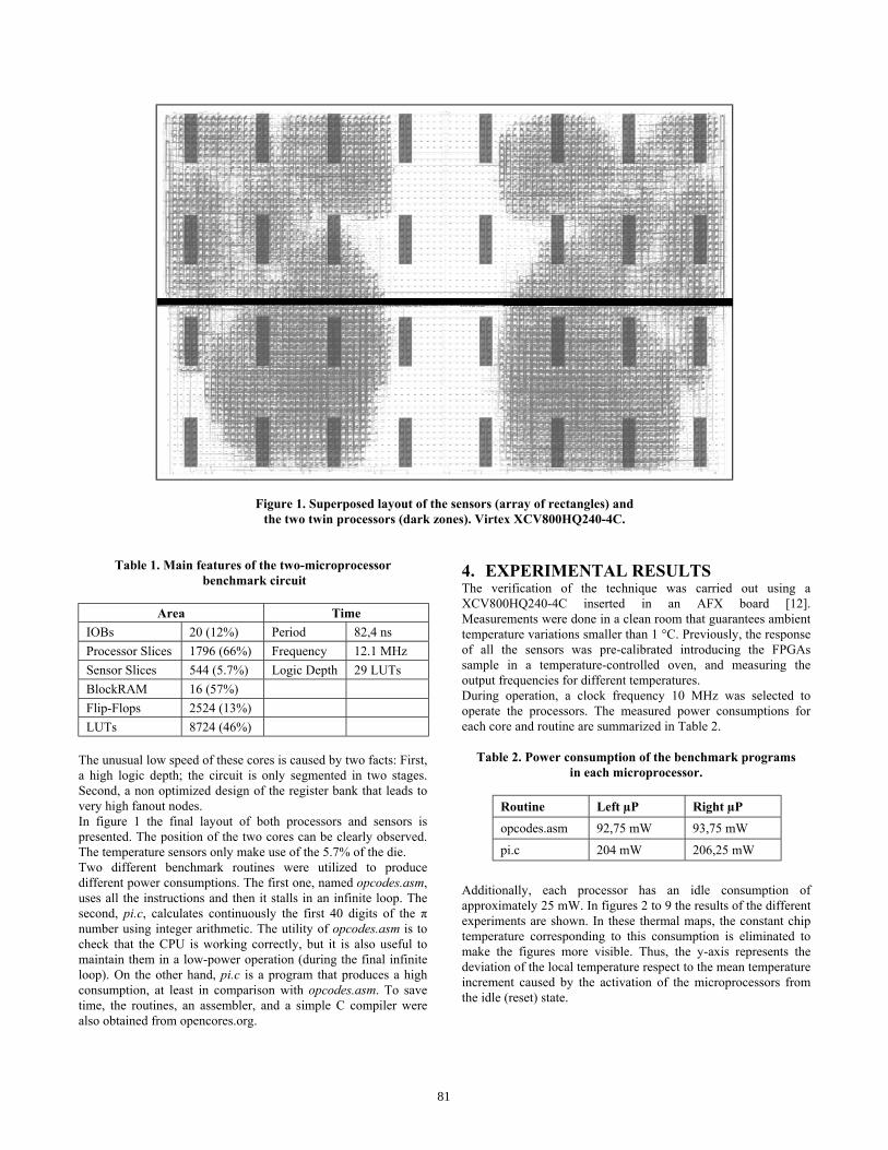
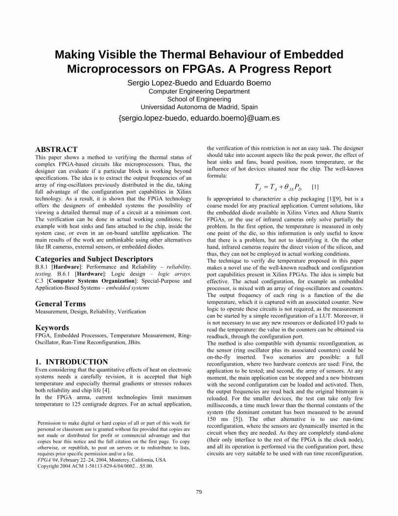
Figure 1. Superposed layout of the sensors (array of rectangles) and the two twin processors (dark zones). Virtex XCV800HQ240-4C.
Table 1. Main features of the two-microprocessor benchmark circuit
Area Time
IOBs 20 (12%) Period 82,4 ns Processor Slices 1796 (66%) Frequency 12.1 MHz Sensor Slices 544 (5.7%) Logic Depth 29 LUTs BlockRAM 16 (57%) Flip-Flops 2524 (13%) LUTs 8724 (46%)
The unusual low speed of these cores is caused by two facts: First, a high logic depth; the circuit is only segmented in two stages. Second, a non optimized design of the register bank that leads to very high fanout nodes. In figure 1 the final layout of both processors and sensors is presented. The position of the two cores can be clearly observed. The temperature sensors only make use of the 5.7% of the die. Two different benchmark routines were utilized to produce different power consumptions. The first one, named opcodes.asm, uses all the instructions and then it stalls in an infinite loop. The second, pi.c, calculates continuously the first 40 digits of the π number using integer arithmetic. The utility of opcodes.asm is to check that the CPU is working correctly, but it is also useful to maintain them in a low-power operation (during the final infinite loop). On the other hand, pi.c is a program that produces a high consumption, at least in comparison with opcodes.asm. To save time, the routines, an assembler, and a simple C compiler were also obtained from opencores.org.
4. EXPERIMENTAL RESULTS The verification of the technique was carried out using a XCV800HQ240-4C inserted in an AFX board [12]. Measurements were done in a clean room that guarantees ambient temperature variations smaller than 1 °C. Previously, the response of all the sensors was pre-calibrated introducing the FPGAs sample in a temperature-controlled oven, and measuring the output frequencies for different temperatures. During operation, a clock frequency 10 MHz was selected to operate the processors. The measured power consumptions for each core and routine are summarized in Table 2.
Table 2. Power consumption of the benchmark programs in each microprocessor.
Routine Left µP Right µP
opcodes.asm 92,75 mW 93,75 mW
pi.c 204 mW 206,25 mW Additionally, each processor has an idle consumption of approximately 25 mW. In figures 2 to 9 the results of the different experiments are shown. In these thermal maps, the constant chip temperature corresponding to this consumption is eliminated to make the figures more visible. Thus, the y-axis represents the deviation of the local temperature respect to the mean temperature increment caused by the activation of the microprocessors from the idle (reset) state.
81
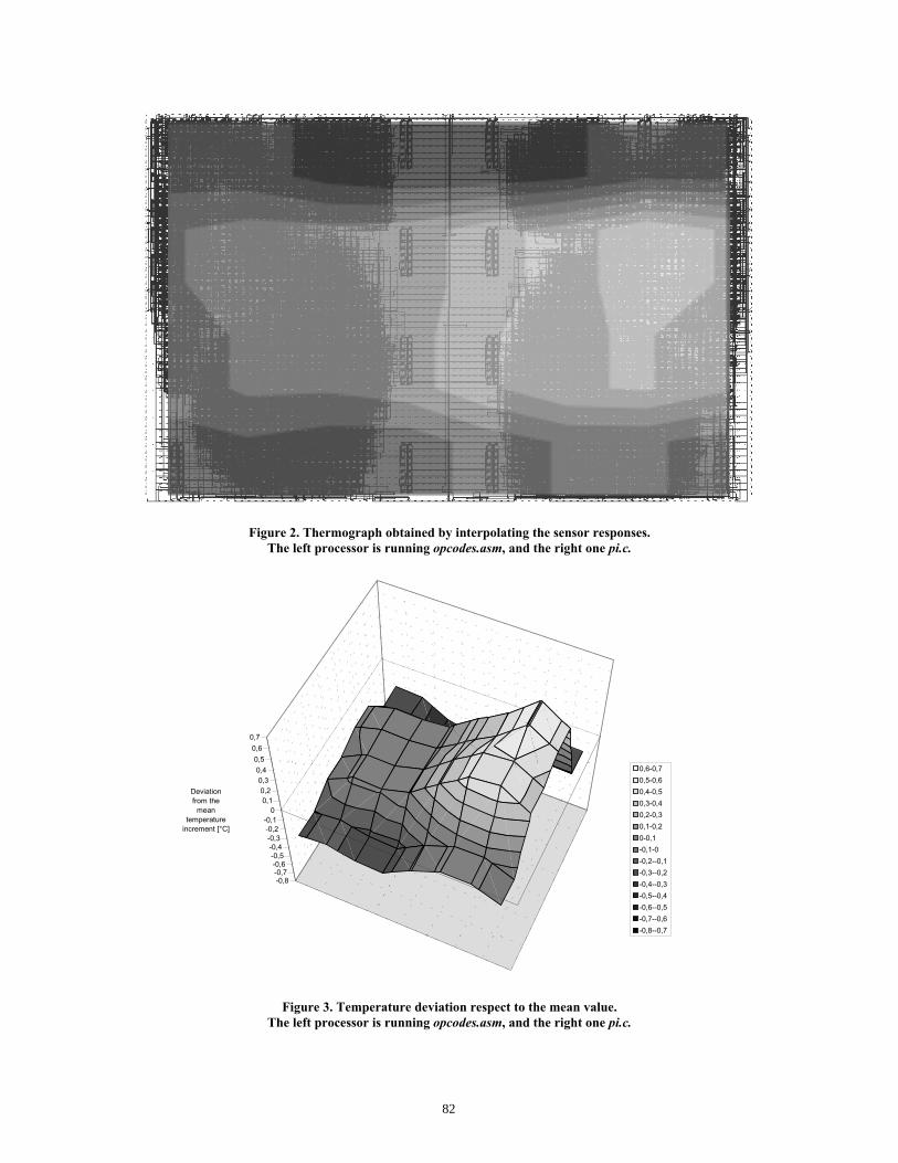
Figure 2. Thermograph obtained by interpolating the sensor responses. The left processor is running opcodes.asm, and the right one pi.c.
-0,8-0,7-0,6-0,5-0,4-0,3-0,2-0,1
00,10,2
0,30,4
0,50,6
0,7
0,6-0,70,5-0,60,4-0,50,3-0,40,2-0,30,1-0,20-0,1-0,1-0-0,2--0,1-0,3--0,2-0,4--0,3-0,5--0,4-0,6--0,5-0,7--0,6-0,8--0,7
Deviation from the
mean temperature
increment [°C]
Figure 3. Temperature deviation respect to the mean value. The left processor is running opcodes.asm, and the right one pi.c.
82

Figure 4. Thermograph obtained by interpolating the sensor responses. The left processor is running pi.c, and the right one opcodes.asm.
-0,8-0,7-0,6-0,5-0,4-0,3-0,2-0,1
00,10,20,3
0,40,5
0,60,7
0,6-0,70,5-0,60,4-0,50,3-0,40,2-0,30,1-0,20-0,1-0,1-0-0,2--0,1-0,3--0,2-0,4--0,3-0,5--0,4-0,6--0,5-0,7--0,6-0,8--0,7
Deviation from the
mean temperature
increment [°C]
Figure 5. Temperature deviation respect to the mean value. The left processor is running pi.c, and the right one opcodes.asm.
83
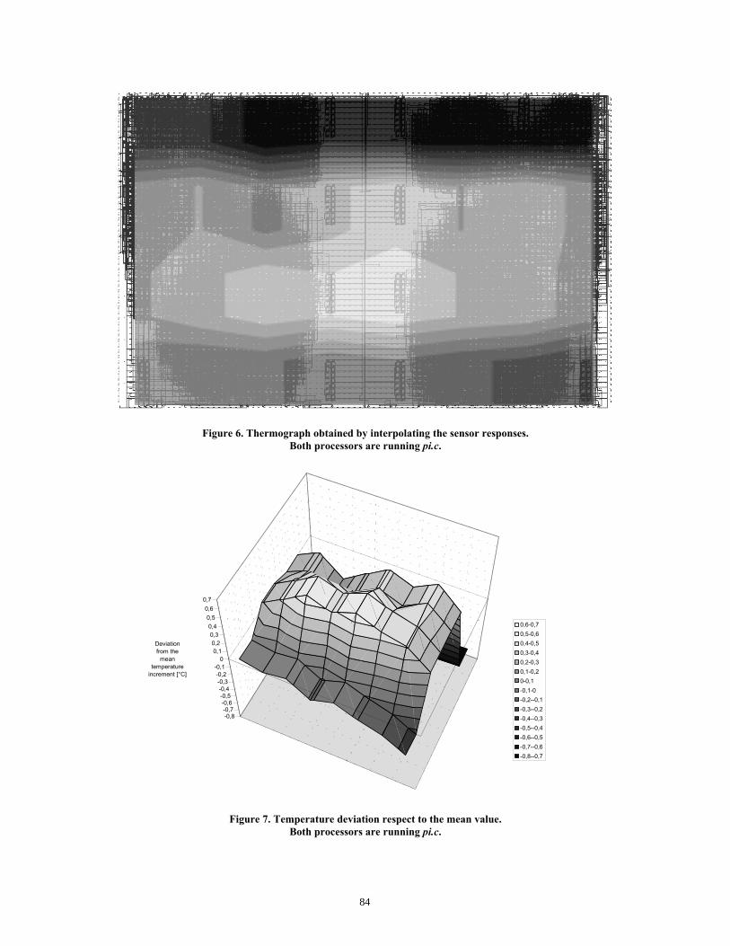
Figure 6. Thermograph obtained by interpolating the sensor responses. Both processors are running pi.c.
-0,8-0,7-0,6-0,5-0,4-0,3-0,2-0,1
00,10,20,30,4
0,50,6
0,7
0,6-0,70,5-0,60,4-0,50,3-0,40,2-0,30,1-0,20-0,1-0,1-0-0,2--0,1-0,3--0,2-0,4--0,3-0,5--0,4-0,6--0,5-0,7--0,6-0,8--0,7
Deviation from the
mean temperature
increment [°C]
Figure 7. Temperature deviation respect to the mean value. Both processors are running pi.c.
84
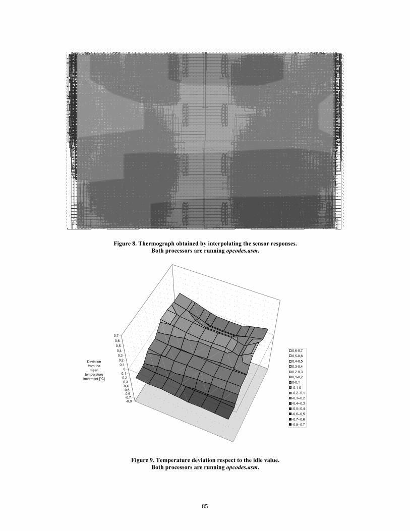
Figure 8. Thermograph obtained by interpolating the sensor responses. Both processors are running opcodes.asm.
-0,8-0,7-0,6-0,5-0,4-0,3-0,2-0,1
00,10,20,3
0,40,5
0,60,7
0,6-0,70,5-0,60,4-0,50,3-0,40,2-0,30,1-0,20-0,1-0,1-0-0,2--0,1-0,3--0,2-0,4--0,3-0,5--0,4-0,6--0,5-0,7--0,6-0,8--0,7
Deviation from the
mean temperature
increment [°C]
Figure 9. Temperature deviation respect to the idle value. Both processors are running opcodes.asm.
85

The figures show that the technique is sensitive enough, even considering the small consumptions involved in the experiments. Is significant the case where a processor runs the heavy program meanwhile the other is hung (figures 2 to 5), because the temperature gradients can be clearly detected. Unfortunately, the processor descriptions utilized in the experiments have no indication of placement. So, the thermal status of the different functional units can not be determined. This information would be useful to redesign the blocks that are producing hot spots. As only exception, a little difference can be observed in the BlockRAM area in Figs. 8 and 9 (where both microprocessors are hung). A small activity is observed, caused by the access to two memory positions that return the JMP and NOP instruction codes.
5. CONCLUSIONS AND FUTURE WORK A new technique, useful to detect hot spots or thermal gradients in FPGA-based circuits, has been presented. Some thermographs have been obtained from a real, complex system utilized as a case-study. The effects of different routines on the thermal status of the chip have been clearly evidenced. As a future work, the effects of the possible voltage drops have to be identified and compensated. This can be done by using two ring oscillators per sensor, with different sensitivities, as outlined in [5], where it is shown that it is possible to simultaneously obtain the temperature and voltage values with errors less than ±1°C and ±5mV. The work opens the door to the design of future EDA tools, which could on-the-fly analyze the activity of the different blocks of a complex circuit implemented on FPGAs. This could be useful for the designer of low-power electronics. He or she could know which block is consuming more power, and thus has to be redesigned, instead of applying a global strategy to reduce power (for example, lowering the clock frequency). The technique is also useful to know, point-to-point of the die, the safety margins respect to the maximum nominal temperature, nowadays situated near 125 ºC. In those applications were thermal deration [3] is still a requirement, this kind of information can save hundred of hours of redesign. Finally, this technique helps to solve one of the peculiarities of FPGA technology, clearly expressed in [10]: “…unlike the power needs of a typical industry Application Specific Integrated Circuit (ASIC) gate array, the Field Programmable device’s power requirement is not determined as the device leaves the factory. Customers' designs can vary in power as well as physical needs. Therein lies the challenge in predicting the FPGA thermal management needs”.
6. ACKNOWLEDGEMENTS This research is supported by project number 07T/0052/2003-3 of the Consejería de Educación de la Comunidad Autónoma de Madrid, Spain.
7. REFERENCES [1] Electronic Industries Association. Integrated Circuits
Thermal Test Method Environmental Conditions - Natural Convection (Still Air). EIA/JEDEC Standard JESD51-2, December 1995.
[2] Guccione S. A. and Levi D. JBits: A Java-based Interface to FPGA Hardware. Xilinx Inc, San Jose, CA, 1998.
[3] Jackson M., Lall P. and Das D. Thermal Deration - A Factor of Safety or Ingnorance. IEEE Trans. on Components, Packaging and Manufacturing Technology, Part A, 20, 1(Mar. 1997), 83-85.
[4] Lall P. Tutorial: Temperature as an Input to Microelectronics-Reliability Models. IEEE Trans. on Reliability, 45, 1(Mar. 1996), 3-9.
[5] Lopez-Buedo S. Tecnicas de verificacion termica para arquitecturas dinamicamente reconfigurables. Ph.D. thesis, in Spanish. Universidad Autonoma de Madrid, Spain. Available at http://www.ii.uam.es/~sergio/tesis.pdf.
[6] Lopez-Buedo S., Garrido J., and Boemo E. Dynamically Inserting, Operating, and Eliminating Thermal Sensors of FPGA-based Systems. IEEE Transactions on Components and Packaging Technologies (CPM), 25, 4(Dec. 2002), 561-566.
[7] Lopez-Buedo S., Garrido J. and Boemo E. Thermal Testing on Reconfigurable Computers. IEEE Design & Test of Computers, 17, 1(Jan.-Mar.) 2000, 84-90.
[8] Rhoads S. The Plasma CPU Core. Available at http://www.opencores.org. September 2001.
[9] Texas Instruments Inc. Package Thermal Characterization Methodologies (Application Report). March 1999.
[10] Xilinx Inc. Packaging Thermal Management. Application Note, July 2002.
[11] Xilinx Inc. Development System Reference Guide – ISE 5. 2002.
[12] Xilinx Inc. Xilinx Prototype Platforms User Guide for Virtex and Virtex-E Series FPGAs. Application Note, December 1999.
86