Embed Size (px)
Citation preview
Magnetron sputtered Gadolina-doped Ceria
Diffusion Barriers for Metal-supported Solid
Oxide Fuel Cells
Steffen Sønderby, Trine Klemensø, Bjarke H. Christensen, Klaus P. Almtoft, Jun Lu, Lars P.
Nielsen and Per Eklund
Linköping University Post Print
N.B.: When citing this work, cite the original article.
Original Publication:
Steffen Sønderby, Trine Klemensø, Bjarke H. Christensen, Klaus P. Almtoft, Jun Lu, Lars P.
Nielsen and Per Eklund, Magnetron sputtered Gadolina-doped Ceria Diffusion Barriers for
Metal-supported Solid Oxide Fuel Cells, 2014, Journal of Power Sources, (267), 452-458.
http://dx.doi.org/10.1016/j.jpowsour.2014.05.101
Copyright: Elsevier
http://www.elsevier.com/
Postprint available at: Linköping University Electronic Press
http://urn.kb.se/resolve?urn=urn:nbn:se:liu:diva-102517
Accepted Manuscript
Magnetron sputtered Gadolinia-doped Ceria Diffusion Barriers for Metal-supportedSolid Oxide Fuel Cells
Steffen Sønderby , Trine Klemensø , Bjarke H. Christensen , Klaus P. Almtoft , JunLu , Lars P. Nielsen , Per Eklund
PII: S0378-7753(14)00794-0
DOI: 10.1016/j.jpowsour.2014.05.101
Reference: POWER 19184
To appear in: Journal of Power Sources
Received Date: 11 November 2013
Revised Date: 6 May 2014
Accepted Date: 20 May 2014
Please cite this article as: S. Sønderby, T. Klemensø, B.H. Christensen, K.P. Almtoft, J. Lu, L.P. Nielsen,P. Eklund, Magnetron sputtered Gadolinia-doped Ceria Diffusion Barriers for Metal-supported SolidOxide Fuel Cells, Journal of Power Sources (2014), doi: 10.1016/j.jpowsour.2014.05.101.
This is a PDF file of an unedited manuscript that has been accepted for publication. As a service toour customers we are providing this early version of the manuscript. The manuscript will undergocopyediting, typesetting, and review of the resulting proof before it is published in its final form. Pleasenote that during the production process errors may be discovered which could affect the content, and alllegal disclaimers that apply to the journal pertain.
MANUSCRIP
T
ACCEPTED
ACCEPTED MANUSCRIPT
1
Magnetron sputtered Gadolinia-doped Ceria Diffusion Barriers for Metal-supported
Solid Oxide Fuel Cells
Steffen Sønderbya,b,*, Trine Klemensøc, Bjarke H. Christensenb, Klaus P. Almtoftb, Jun Lua, Lars P.
Nielsenb, and Per Eklunda
aThin Film Division, Department of Physics, Chemistry and Biology, IFM, Linköping University,
SE-581 83 Linköping, Sweden
bDanish Technological Institute, Tribology Centre, Teknologiparken, Kongsvang Allé 29, DK-8000
Aarhus C, Denmark
cDepartment of Energy Conversion and Storage, Technical University of Denmark,
Frederiksborgvej 399, DK-4000 Roskilde, Denmark
*Corresponding author. Tel: +45-7220 2795; Fax: +45-7220 1550; E-mail: [email protected]
Keywords: Physical Vapor deposition (PVD); Solid Oxide Fuel Cell (SOFC); GDC; CGO
MANUSCRIP
T
ACCEPTED
ACCEPTED MANUSCRIPT
2
Abstract
Gadolinia-doped ceria (GDC) thin films are deposited by reactive magnetron sputtering in an
industrial-scale setup and implemented as barrier layers between the cathode and electrolyte in
metal-based solid oxide fuel cells consisting of a metal support, an electrolyte of ZrO2 co-doped
with Sc2O3 and Y2O3 (ScYSZ) and a Sr-doped lanthanum cobalt oxide cathode. In order to optimize
the deposition of GDC to obtain high electrochemical performance of the cells, the influence of film
thickness and adatom mobility is studied. The adatom mobility is varied by tuning the deposition
temperature and substrate bias voltage.
A GDC layer thickness of 0.6 µm is found to effectively block Sr diffusion when bias voltage and
deposition temperature is tuned to promote dense coatings. The adatom mobility has a large
influence on the film density. Low temperature and bias voltage result in underdense column
boundaries which function as channels for Sr to diffuse to the GDC-ScYSZ interface. By tuning
deposition temperature, bias voltage and film thickness area specific resistances down to 0.34 Ωcm2
are achieved at cell tests performed at an operating temperature of 650 °C.
.
MANUSCRIP
T
ACCEPTED
ACCEPTED MANUSCRIPT
3
1. Introduction
At intermediate temperatures, metal-supported solid oxide fuel cells (SOFCs) designs are of interest
as an alternative to ceramic supported cells in view of their low materials cost and high robustness,
which is advantageous both in the production line and in applications such as auxiliary power units
[1]. During fabrication of metal-supported cells, care must be taken to avoid corrosion of the steel
components. This involves processing at lower temperatures or in reducing atmospheres. Therefore
traditional cathodes developed for ceramic cells, such as (La,Sr)MnO3−δ (LSM) and
(La,Sr)(Co,Fe)O3−δ (LSCF)), cannot be transferred directly to metal-supported cells, as these
cathodes requires sintering in air at 1000–1200 °C to achieve good adhesion of the cathode [1].
(La,Sr)CoO3−δ (LSC) is another cathode material which has been found to be suitable for metal-
supported cells as it sinters readily at temperatures below 900 °C and has a good electrochemical
performance at intermediate temperatures [2, 3]. However, LSC is incompatible with yttria-
stabilized zirconia (YSZ) traditionally used for SOFC electrolytes, as strontium from the cathode
reacts with zirconium from the electrolyte to form SrZrO3 which has a low ionic conductivity [4, 5,
6] and therefore a detrimental effect on cell performance. This reaction is known to take place
during sintering at temperatures above 1000 °C [7] but has also been observed at intermediate
temperatures down to 650 °C [5, 8]. To avoid this reaction a gadolinia-doped ceria (GDC) barrier
can be applied between electrolyte and cathode. Several studies have shown the suitability of GDC
as a barrier for Sr diffusion [3, 9, 10, 11]. GDC can be applied by screen printing, spraying, or tape
casting followed by sintering at temperatures above 1200 °C. In itself GDC is an excellent ionic
conductor but at these temperatures a solid solution of YSZ and GDC is formed which has
significantly lower oxide ion conductivity than the pure form of both compounds [7,12,13].
Alternatively the GDC barrier can be applied by physical vapor deposition (PVD) techniques such
as pulsed laser ablation [7], electron beam evaporation [14], or magnetron sputtering [3, 11, 15, 16].
MANUSCRIP
T
ACCEPTED
ACCEPTED MANUSCRIPT
4
GDC barriers prepared by PVD techniques stops Sr diffusion better than barriers prepared by wet
ceramic techniques. This may be due to higher density of such layers [3, 11], which can be achieved
at lower temperatures. Low-temperature deposition is particularly important for metal-supported
cells, which cannot withstand as high temperatures as ceramic cells. When depositing on metal-
supported cells it is reasonable to set 400 °C as the upper limit deposition temperature as the oxygen
present for the reactive deposition process may oxidize the metal-support at elevated temperateres
which reduces cell performance. When synthesizing GDC coatings for ceramic SOFCs high
deposition temperatures are often used to grow coatings sufficiently dense to prevent Sr diffusion
[11, 17]. In a recent study, we showed using a model system that the main route for Sr diffusion in
sputtered GDC films are along underdense column boundaries which can be densified and/or
limited by increasing the adatom mobility[18]. Besides the deposition temperature, other ways to
increase adatom mobility includes increasing the ionization degree of the plasma and applying a
substrate bias. Especially the combination of elevated temperatures and the application of substrate
bias has been found to be an effective method to tune the microstructure when depositing GDC for
ceramic-supported SOFC [16].
In this work, the influence of substrate bias voltage, film thickness, and deposition temperature on
reactively sputtered GDC barriers for metal-supported cells are investigated. The purpose of the
study is twofold. First, we demonstrate how deposition of GDC can be tuned to form effective
diffusion barriers to metal-supported cells. Furthermore, we prove the Sr diffusion mechanism to be
as previously demonstrated in a model system [18].
2. Experimental details
GDC (Ce0.9Gd0.1O2−δ) coatings were deposited by reactive pulsed magnetron sputtering using a
CC800/9 SinOx industrial batch coater from CemeCon AG. Two metallic Ce–Gd targets (90:10
at.%) with purity 99.9 % and size 88×500 mm2 were sputtered in mixed Ar/O2 atmosphere. The
MANUSCRIP
T
ACCEPTED
ACCEPTED MANUSCRIPT
5
purity of the applied gasses were 99.999 %. The coatings were grown on 20×20 mm2 metal-
supported half cells mounted on a stage carrying out a two-fold planetary rotation during
deposition. The half cells consisted of a metal support and a ScYSZ (ZrO2 co-doped with Sc2O3 and
Y2O3) electrolyte. Before starting the deposition the chamber was pumped down to a base pressure
below 1 mPa and the substrates were heated to a temperature slightly higher than the deposition
temperature of either 300 °C or 400 °C. The total pressure was 0.4 Pa during deposition. A pulsed
DC power supply (Advanced Energy, Pinnacle II) delivered 2 kW to each sputtering target with a
repetition frequency of 50 kHz and a duty cycle of 50 %. Before the deposition series, the voltage
hysteresis loop for the system was determined. The films were deposited operating in the transition
region between the metallic and poisoned state of the targets in order to obtain both high deposition
rate and stoichiometric films. In order to run the system in the transition region, the cathode current
was used as an oxygen partial-pressure feedback signal for controlling the reactive sputtering
process. A pulsed DC bias with a frequency of 350 kHz and a reverse time of 1 µs was applied to
the mounting stage/samples and used to vary the kinetic energy of ions bombarding the growing
film. In order to study the influence of deposition parameters on the ability of the GDC barrier
coatings to prevent Sr diffusion, three sets of depositions were performed where the substrate bias
voltage, deposition temperature, and film thickness were varied, respectively.
The metal-supported half cells used in this work were fabricated by tape casting of the metal-
support (a 22% Cr-based stainless steel alloy), the cermet backbone and the ScYSZ electrolyte
followed by co-sintering in a reducing H2/Ar atmosphere under proprietary conditions above 1000
°C. The active fuel cell anode was formed by infiltrating the porous metal-support and cermet with
the electrocatalytic active Ce0.8Gd0.2O1.9 and Ni. The fabrication procedure and infiltration route of
the metal-supported half-cells is described in detail elsewhere [19]. After deposition of the GDC
barrier coating on the ScYSZ electrolyte layer, cathodes with a composition of 50 vol.% GDC -
MANUSCRIP
T
ACCEPTED
ACCEPTED MANUSCRIPT
6
50vol.% LSC (La0.6Sr0.4)0.99CoO3-δ) were printed with an area of 0.5 cm2. The cathode layer was
fired in situ in air flow during the cell test start-up at a maximum temperature of 800 °C.
The cells were tested in a set-up also described in [3]. Platinum meshes placed in parallel with the
cell were used to contact the cell to the set-up, and the fuel and oxidant gas was supplied to the cell
via alumina tubes perpendicular to the cell active area. Polarization curves were collected at 650 °C,
with fuel consisting of 4 vol.% H2O-96 vol.% H2 on the anode side, and air or O2 on the cathode
side, and using flows of 100 ml/min (equivalent to 6 L/h).
Scanning electron microscopy (SEM, Nova 600 nanoSEM from FEI) was performed on cross-
sections of the samples in order to determine the thickness and morphology of the GDC barrier. In
order to prepare the samples for SEM they were either vacuum embedded in Epofix (Struers,
Denmark), and polished to 1 µm or simply broken into two pieces. Scanning transmission electron
microscopy (STEM) and energy dispersive X-ray spectroscopy (EDX) were performed on film
cross-sections using a Tecnai G2 TF 20 U-Twin 200 kV FEGTEM from FEI. Cross-section samples
were prepared by mechanically polishing down to a thickness of approximately 55 µm followed by
ion milling using Precision Ion Polishing System (PIPS; Gatan) operated at 5 keV and 5 ° incident
angle with argon ions and a final polishing step at 2 keV for 10 min. X-ray diffraction (XRD)
measurements in the θ–2θ geometry were carried out with a Bruker D8 Discover diffractometer
using CuKα radiation. Single-line profile analysis was performed with the TOPAS 2.1 [20] software
using a pseudo-Voigt peak profile [21]. The size of the coherently diffracting domains, which was
used as a measure for the average grain size, and the microstrain were determined from the integral
breadths of the Lorentzian and Gaussian constituents of the pseudo-Voigt function, respectively.
A few as-deposited GDC barriers were annealed in a tube furnace (Heraeus, Ro 4/25) in an Ar
atmosphere in order to study effect of elevated temperatures on the film microstructure.
3. Results and discussion
MANUSCRIP
T
ACCEPTED
ACCEPTED MANUSCRIPT
7
3.1 Influence of adatom mobility on the GDC barrier
In order to study the effect of adatom mobility on the ability of the GDC barrier to prevent Sr
diffusion, two series of depositions were carried out where either the substrate bias or the deposition
temperature was varied. The application of elevated deposition temperatures or bias voltages are
two different ways of providing energy to the growing film. For the study of the effect of bias
voltage, films with a thickness of approximately 600 nm were deposited at 400 °C with applied
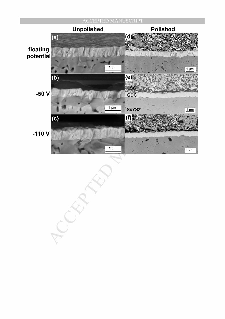
substrate bias voltage of -110 V, - 50V, and at floating potential. Figure 1 shows SEM images from
unpolished cross-sections of the as-deposited films (left) and from polished cross-sections of tested
cells containing these films (right). From the unpolished fracture cross-sections it is seen that all
films are columnar. When looking at the polished cross-sections the columnar structure is not
visible in the GDC barriers deposited at -110 V and -50 V while it is clearly seen in the coating
deposited at floating potential. In fact the columnar structure is present in all films (verified by
TEM) but cannot be distinguished in polished cross-section of films deposited with applied bias.
This reveals that the film deposited at floating potential is less dense than films deposited while
applying a bias voltage. The open structure observed at floating potential is due to low adatom
mobility during film growth, whereas the films grown under the influence of applied substrate bias
becomes denser as energetic gas ions bombard the growing film and increase adatom mobility
resulting in better closing of voids [22].
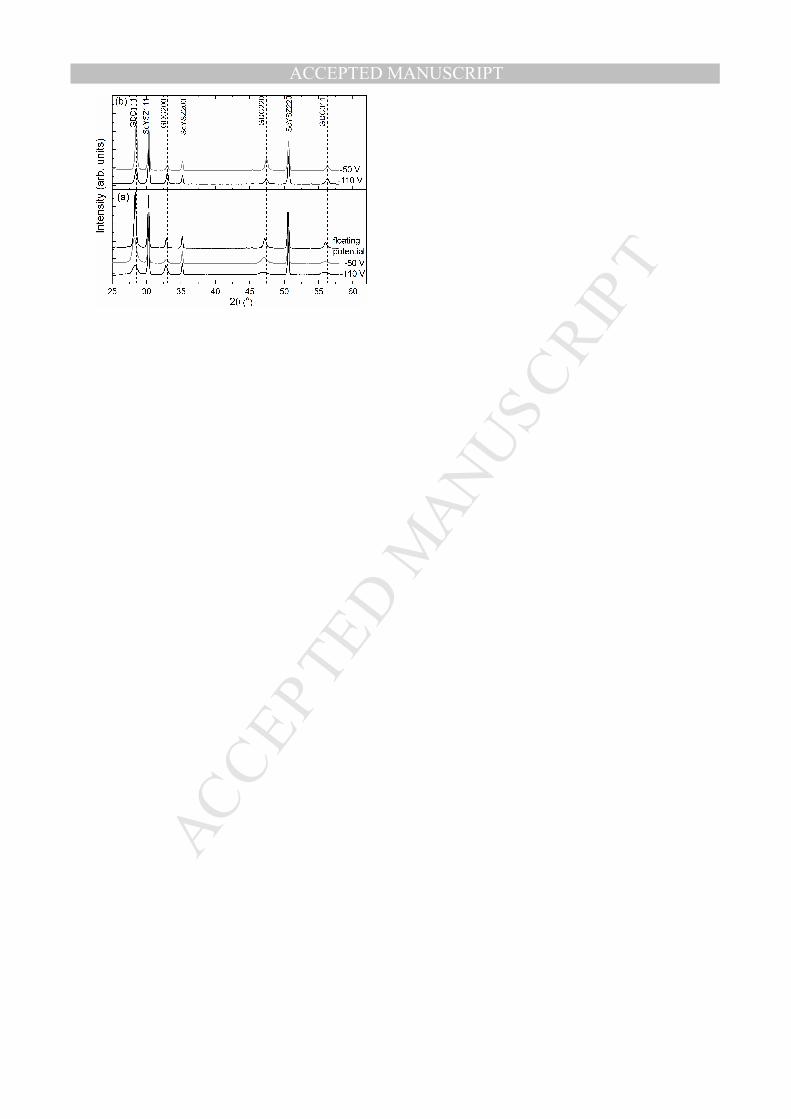
Figure 2.a shows X-ray diffractograms of the films deposited at different bias voltages. Peaks from
both the deposited GDC layer and the ScYSZ electrolyte are seen. From the X-ray diffractogram the
ScYSZ electrolyte can be seen to consist of randomly oriented grains as all peaks for cubic ScYSZ
are seen. All peaks for cubic GDC (ICDD JCP2 No. 75-161) are also present revealing that the
GDC is not textured as well. The peak positions from the database are marked by dotted lines. It is
seen that all peaks of the as-deposited films are found at slightly lower angles than the reference
MANUSCRIP
T
ACCEPTED
ACCEPTED MANUSCRIPT
8
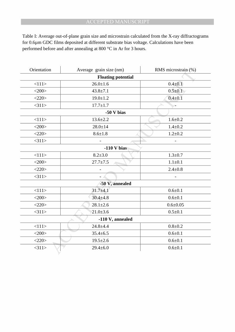
from the database. This reveals the films are compressively stressed. Table I shows average out-of-
plane grain sizes and microstrains, as calculated in the single-line profile analysis. The average in
grain size is dependent on the grain orientation; however, in general a decreasing grain size is
obtained with increasing negative bias voltage. In contrast, the microstrain is seen to increase from
~0.5 % at floating potential to above 1 % at -50 V and -110 V. This relation is generally seen when
preparing films by sputtering using high bias voltages since the energetic ion flux inhibits grain
growth and induces defects (microstrain) and compressive stress [22]. It has previously been found
that grain size, film stress and microstrain affect the ionic conductivity of GDC and other ionic
conductors [23,24,25,26]. Investigations have shown the grain size to influence the ionic conduction
as grain boundary conductivity was higher than bulk conductivity [27,28] and has therefore been
studied as a way of increasing the overall ionic conductivity of SOFC electrolytes [29]. However,
the effect of grain size is still debated due to a large scatter in reported results and it has been
proposed that other parameters such as lattice strain needs to be considered as well [24]. Studies of
stress effects on the ionic conductivity of fluorite structures have shown that a small tensile stress
could increase the conductivity [30], while a decrease in conductivity by compressive stress was
observed [26]. Elevated temperatures, as the ones the cells are exposed to during cathode sintering
and operation, are known to cause stress release and grain growth. Therefore, films deposited at -50
V and -110 V bias were annealed at 800 °C for 3 hours. Fig. 2.b shows X-ray diffractograms of
annealed samples. Compared to as-deposited samples (fig.2.a) the GDC peak positions have moved
to higher angles and are now found at the same angles as the powder reference. This shows the
compressive stresses in the films have been released. As seen in Table I this treatment also results in
grain coarsening and a reduction in microstrain compared to the respective as-deposited samples.
After annealing the average grain sizes of the films are comparable which was not the case prior to
annealing. The same is seen for the microstrain. As these differences are equalized in the annealing
MANUSCRIP
T
ACCEPTED
ACCEPTED MANUSCRIPT
9
experiment it is reasonable to believe that the same would happen during cathode sintering.
Therefore, the deposition-related differences in film stress, grain size, and microstrain are not
thought to affect the ionic conductivity in this case.
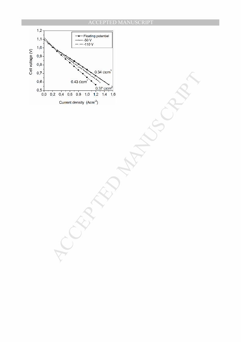
Polarization curves recorded at 650 °C for button cells with 0.6 µm thick GDC barriers deposited at
different substrate bias voltage is shown in Figure 3. The initial OCV (open circuit voltages)
indicated a leak-tight set-up, with an OCV of 1.12 V for floating and -110 V, and 1.10 V for -50 V.
For comparison, the theoretical OCV at 650 °C with 4 vol% H2O-96 vol% H2 as fuel and air as
oxidant is 1.11 V, and the observed differences to this value is believed to be due to minor
variations in the steam content which is known to affect OCV significantly. The cell containing the
GDC barrier deposited at floating potential has the highest area-specific resistance (ASR) of 0.43
Ωcm2 whereas the ASR values of the cells with GDC barriers deposited at -50 V and -110 V bias
are 0.34 Ωcm2 and 0.37 Ωcm2, respectively. Comparing the measured ASR to the microstructure of
GDC thin films (Fig. 1) it is seen that the film deposited at floating potential has the most open
microstructure while films deposited at an applied bias are denser and do not display any significant
difference which is replicated in the ASR values. To study the relationship between ASR and
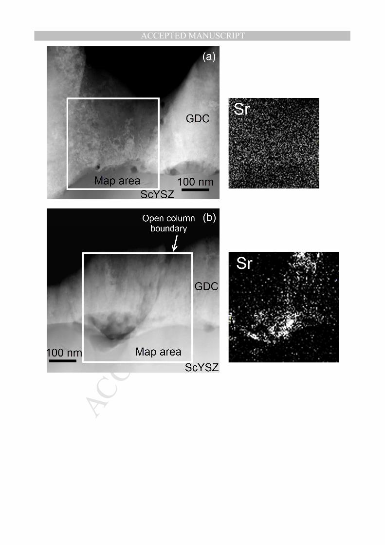
microstructure in detail STEM micrographs and EDX mappings of the GDC-ScYSZ interface from
samples deposited at floating potential and -50 V substrate bias were obtained, see Figure 4. Fig. 4a
shows STEM/EDX mapping of a cross-section of the film grown at -50 V which displays a dense
microstructure. The columnar structure of the film is seen and there are no voids between the
columns. Furthermore, the EDX mapping shows that no Sr diffusion has taken place. Fig. 4b shows
a cross-section of a sample deposited at floating potential which has a more open microstructure.
The micrograph has been acquired at a position of an open column boundary that may be
comparable to the ones observed in Fig. 1d. The EDX mapping shows Sr diffusion has taken place
at this position. Therefore, the high ASR obtained with a barrier deposited at floating potential can
MANUSCRIP
T
ACCEPTED
ACCEPTED MANUSCRIPT
10
be related to the formation of SrZrO3 at the GDC-YSZ interface as the open microstructure fails to
stop Sr diffusion along the column boundaries in sputtered GDC films. This is in accordance with
the results seen in our previous study of Sr diffusion in a model system imitating a SOFC setup
[18].
The difference in ASR between the films deposited at -50 V and -110 V is 0.03 Ωcm2 which is too
small to attribute it to differences in the GDC layer with certainty, and 0.03 Ωcm2 is within the
uncertainty that can be related to other cell components such as small deviations in the anode and
cathode performance. For comparison, it should be noted that a cell with a spin-coated GDC barrier
under similar condition has an ASR of 0.50 Ωcm2 meaning the sputtered barriers provide a
considerable improvement as previously reported [3].
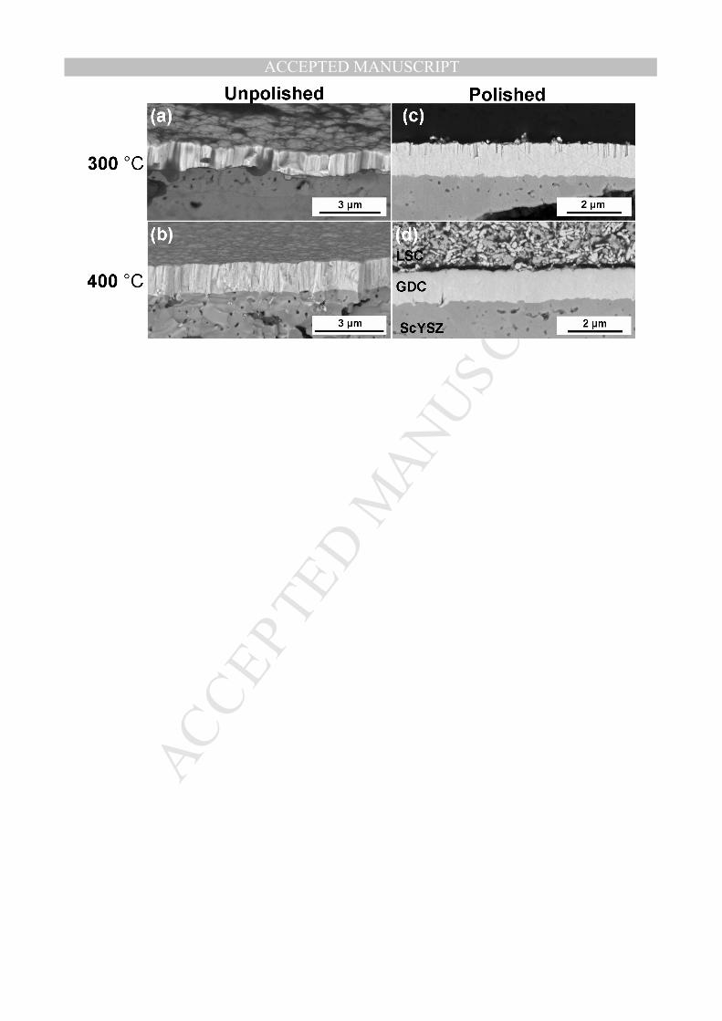
Approximately 1.2 µm thick films were deposited at -50 V substrate bias and 300 °C and 400 °C in
order to study the temperature effect on adatom mobilty and the film densification it provides. -50
V bias was chosen, as this bias voltage had shown good results in cell tests as seen in Fig. 3. The
film thickness was doubled in comparison to the study on the effect of bias voltage to gain
information on the influence of film thickness as well. Figure 5 displays cross-sectional SEM
images of deposited GDC coatings. In both cases the unpolished cross-sections (Fig. 5.a and 5.b)
show the deposited films are coloumnar but the columns of the film deposited at 300 °C are more
easily distinguished. In the polished cross sections (Fig. 5.c and 5.d) the columnar structure is still
visible in the the film deposited at 300 °C whereas it is not observed in the film deposited at 400 °C
which shows the film deposited at 300 °C to be less dense.
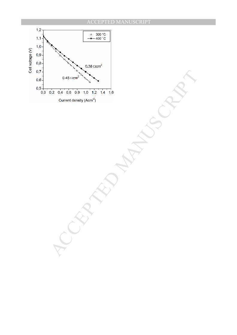
Polarization curves for cells with GDC barriers deposited at 300 °C and 400 °C, respectively, is
seen in Figure 6. The cell having a GDC barrier deposited at 300 °C is seen to have the highest ASR
of 0.45 Ωcm2 compared to 0.38 Ωcm2 for the cell with the GDC barrier deposited at 400 °C. The
high ASR of the first mentioned cell is comparable to the ASR of the cell with a GDC barrier
MANUSCRIP
T
ACCEPTED
ACCEPTED MANUSCRIPT
11
deposited at 400 °C but without the application of substate bias (0.43 Ωcm2, see Fig. 3). A columnar
structure of the GDC barriers is also visible in the polished SEM cross-sections for both of these
cells (fig. 1.d and 5.c). Therefore, it is reasonable to believe the same mechanism of Sr diffusion to
the YSZ-GDC interface along column boundaries in the underdense film causes the high ASR.
In this study, the use of metal-supported cells sets 400 °C as the upper limit for the deposition
temperature as the oxygen present for the reactive deposition process may oxidize the metal-support
at elevated temperatures which will reduce cell performance. Therefore, it is irrelevant for the
present study if higher temperatures can further densify the barrier.
3.3 Influence of film thickness on the GDC barrier
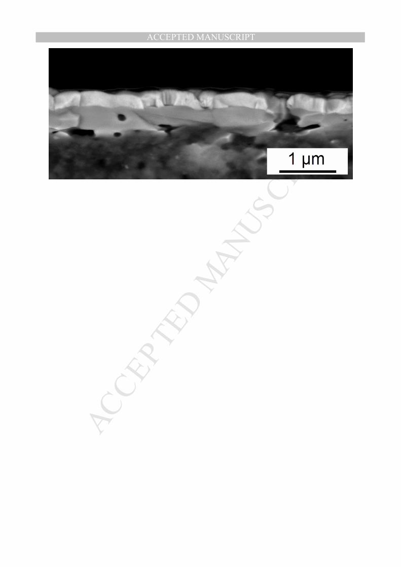
The influence of GDC film thickness was investigated by depositing films with different
thicknesses at -50 V substrate bias and 400 °C. Figure 7 shows an unpolished SEM cross section of
a 0.3 µm thick GDC coating. Comparable films at other thicknesses are seen in Fig. 1.b (0.6 µm)
and Fig 5.b (1.2 µm). A columnar structure is clearly visible at for the 0.6 µm and 1.2 µm thick
films while it is less visible for the 0.3 µm thick film. All polished cross-sections (not shown for the
0.3 µm thick film) appear featureless. In contrast to the thicker films, the 0.3 µm film shown in Fig.
7 is not dense as it is too thin to provide an adequate coverage of surface defects in the substrate.
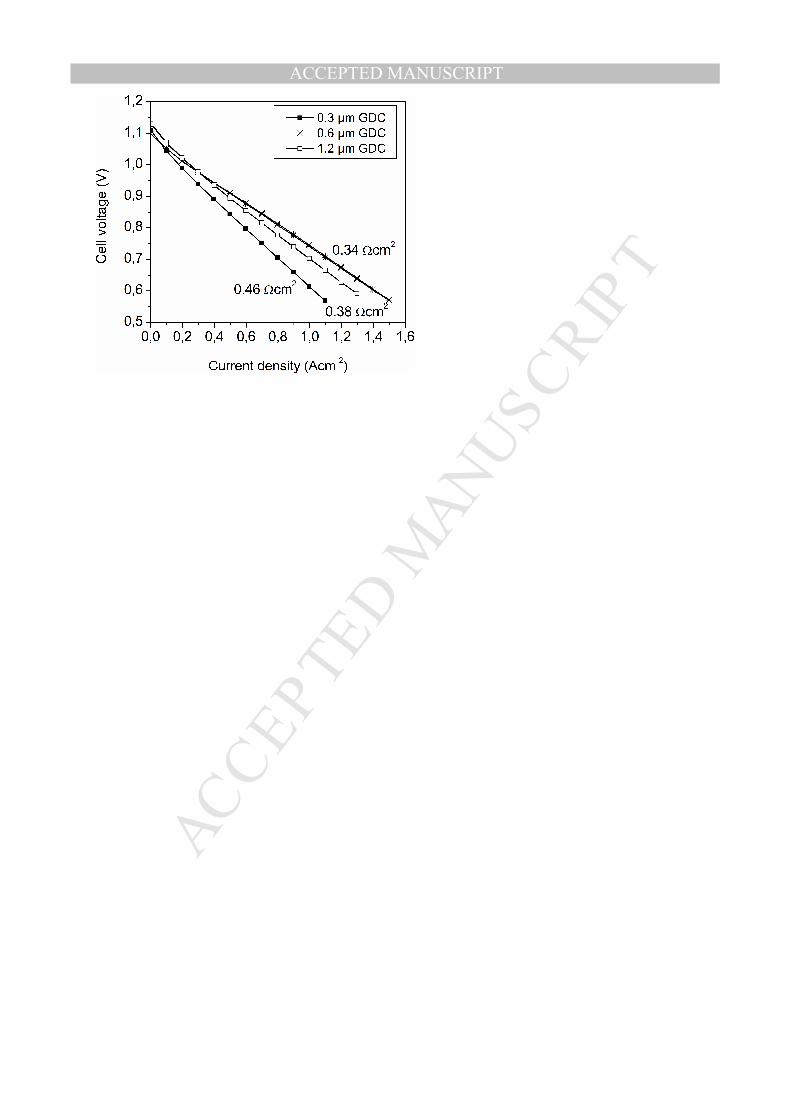
Figure 8 shows polarization curves for cells containing GDC barriers of different thicknesses. The
cell having a 0.3 µm thick GDC barrier has the highest ASR of 0.46 Ωcm2 while the ASR of the
other cells were 0.38 Ωcm2 (1.2 µm GDC barrier) and 0.34 Ωcm2 (0.6 µm GDC barrier). The high
ASR measured for the cell with 0.3 µm GDC can be related to the incomplete coverage of this
barrier which allows Sr diffusion and zirconate formation. The increase in ASR as the thickness is
doubled from 0.6 µm to 1.2 µm cannot be ascribed the increased ohmic resistance of the thicker
GDC layer. In literature the conductivity of GDC in generally stated to be around 0.03 Scm-1 at 650
MANUSCRIP
T
ACCEPTED
ACCEPTED MANUSCRIPT
12
°C [31,32] which means a thickness increase of 600 nm would result in an ASR increase in the
range of 0.002 Ωcm2 meaning most of the difference of 0.04 Ωcm2 is related to other cell
components. Based on these observations it seems that while 0.3 µm GDC is too thin to effectively
avert Sr diffusion, 0.6 µm GDC prevents the diffusion. Any further increase in GDC thickness does
not improve performance as the 0.6 µm thick layer has effectively prevented Sr diffusion. This is of
interest from a production point of view as unnecessary materials use and process time can be
reduced.
4. Conclusion
GDC thin films have been deposited onto ScYSZ electrolytes and implemented into metal-
supported SOFCs. In order to optimize the electrochemical performance of the cells the influence of
bias voltage, deposition temperature and GDC layer thickness was studied.
Films grown at floating potential were found to have an open microstructure in contrast to films
deposited with an applied bias that could activate adatom diffusion and produce denser films. As a
result, an area specific resistance (ASR) of 0.43 Ωcm2 was measured in cell test for a film deposited
at floating potential whereas a film deposited at -50 V bias gave an ASR of 0.34 Ωcm2. STEM/EDX
investigations showed Sr diffusion to occur along the open column boundaries which is in
accordance with results of our previous study of Sr diffusion in a model system. Besides densifying
the films bias voltage also resulted in smaller grain sizes and induced microstrain and compressive
stress in the film. However, heat treatment of the samples resulted in stress release, grain coarsening
and reduction of defects (microstrain) which made the microstructure of the films comparable
meaning that these as-deposited film differences had no effect after cathode sintering.
Deposition temperature was seen to have a large impact on the adatom mobility and subsequently
film density. Films deposited as 300 °C and 400 °C had ASR values of 0.45 Ωcm2 and 0.38 Ωcm2,
MANUSCRIP
T
ACCEPTED
ACCEPTED MANUSCRIPT
13
respectively and SEM images showed the microstructure of the film deposited at 300 °C to be less
dense. Temperatures above 400 °C were not investigated as it was not desired to go to higher
temperatures in order to prevent oxidation damages to the metal-support during the deposition
process.
It was found that 0.6 µm of GDC effectively blocked Sr diffusion when depositions were carried
out at 400 °C and with the application of bias. 0.3 µm of GDC was not enough to properly cover the
substrate due to surface roughness and resulted in a high ASR. For films thicker than 0.6 µm no
further improvement of the electrochemical performance was seen as the Sr diffusion was already
stopped by the initial 0.6 µm of GDC.
Acknowledgments
Financial support from Nordforsk ref. no. 9046 (ThinSOFT), Nordic Innovation Centre ref. no.
09046 (Thin-SOFC), the Swedish Foundation for Strategic Research (Ingvar Carlsson Award 3 and
Future Research Leaders 5), Topsoe Fuel Cell A/S and the Danish National Advanced Technology
Foundation is acknowledged.
References:
[1] M. C. Tucker, J. Power Sources 195 (2010) 4570–4582 [2] R. Maric, R. Neagu, Y. Zhang-Steenwinkel, F. P.F. van Berkel, B. Rietveld, J. Power Sources 195 (2010) 8198–8201. [3] T. Klemensø, J. Nielsen, P. Blennow, Å. H. Persson, T. Stegk, B. H. Christensen, S. Sønderby, J. Power Sources 196 (2011) 9459–9466. [4] F. W. Poulsen, N. van der Puil, Solid State Ionics 53-56 (1992) 777–783. [5] M. Sase, D. Ueno, K. Yashiro, A. Kaimai, T. Kawada, J. Mizusaki, J. Phys. Chem. Solids 66 (2005) 343–348.
MANUSCRIP
T
ACCEPTED
ACCEPTED MANUSCRIPT
14
[6] Andre Heel, Peter Holtappels, Thomas Graule, J. Power Sources 195 (2010) 6709–6718. [7] R. Knibbe, J. Hjelm, M. Menon, N. Pryds, M. Søgaard, H.J. Wang, K. Neufeld, J.Am. Ceram. Soc. 93 (9) (2010) 2877–2883. [8] H.-S. Noh, J.-W. Son, H. Lee, J.-S. Park, H.-W. Lee, J.-H. Lee, Fuel Cells 10 (2010) 1057–1065. [9] S. Uhlenbruck, N. Jordan, J.M. Serra, H.P. Buchkremer, D. Stöver, Solid State Ionics 181 (2010) 447–452. [10] P. Plonczak, M. Joost, J. Hjelm, M. Søgaard, M. Lundberg, P. V. Hendriksen, J. Power Sources 196 (2011) 1156–1162. [11] N. Jordan, W. Assenmacher, S. Uhlenbrucka, V.A.C. Haanappel, H.P. Buchkremer, D. Stöver, W. Mader, Solid State Ionics 179 (2008) 919–923. [12] A. Tsoga, A. Gupta, A. Naoumidis, P. Nikolopoulos, Acta Mater. 2000, 48, 4709–4714. [13] A. Tsoga, A. Naoumidis, D Stöver, Solid State Ionics 2000, 135, 403–409. [14] Y.S. Hong, S.H. Kim, W.J. Kim, H.H. Yoon, Curr. Appl Phys. 11 (2011) S163–S168. [15] Y.-L. Kuo, C. Lee, Y.-S. Chen, H. Liang, Solid State Ionics 180 (2009) 1421–1428. [16] F. C. Fonseca, S. Uhlenbruck, R. Nédélec, D. Sebold, H. P. Buchkremer, J. Electrochem. Soc. 157 (2010) B1515-B1519. [17] S. Uhlenbruck , N. Jordan, D. Sebold, H.P. Buchkremer, V.A.C. Haanappel, D. Stöver, Thin Solid Films 515 (2007) 4053–4060
[18] S. Sønderby, P. Lunca Popa, J. Lu, B. H. Christensen, K. P. Almtoft, L. P. Nielsen, and P. Eklund Adv. Energy Mater. 3 (2013) 923–929. [19] P. Blennow, J. Hjelm, T. Klemensø, S. Ramousse, A. Kromp, A. Leonide, A. Weber, J. Power Sources 196 (2011) 7117-7125. [20] Diffracplus TOPAS P 2.1, Bruker AXS GmbH D-76187 Karlsruhe, Germany, 2003. [21] Th. H. de Keijser, J. I. Langford, E. J. Mittemeijer, and A. B. P. Vogels, J. Appl. Crystallogr. 15 (1982) 308–314. [22] I. Petrov, P.B. Barna, L. Hultman, J.E. Greene, J. Vac. Sci. Technol., A 21 (2003) S117–128. [23] M. Swanson, N. Tangtrakarn, M. Sunder, P.D. Moran, Solid State Ionics 181 (2010) 379–385.

MANUSCRIP
T
ACCEPTED
ACCEPTED MANUSCRIPT
15
[24] J. L. M. Rupp,Solid State Ionics 207 (2012) 1–13. [25] J. L. M. Rupp, L. J. Gauckler, Solid State Ionics 177 (2006) 2513–2518. [26] N. Schichtel, C. Korte, D. Hesse and J. Janek, Phys. Chem. Chem. Phys. 11 (2009) 3043–3048. [27] G. Knöner, K. Reimann, R. Röwer, U. Södervall, H.-E. Schaefer, Proc. Natl. Acad. Sci. U.S.A. 100 (2003) 3870-3873. [28] W. Jung, J. L. Hertz, and H. Tuller, Acta Mater. 57, (2009) 1399 -1404. [29] J. Maier, Nature Mater. 4 (2005) 805-815. [30] W. Araki, Y. Imai, T. Adachi, J. Eur. Ceram. Soc. 29 (2009) 2275–2279. [31] H. Inaba, H. Tagawa, Solid State Ionics 83 (1996) 1–16. [32] D.W. Jung, K. L. Duncan, E. D. Wachsman, Acta Mater. 58 (2010) 355–363.
MANUSCRIP
T
ACCEPTED
ACCEPTED MANUSCRIPT
16
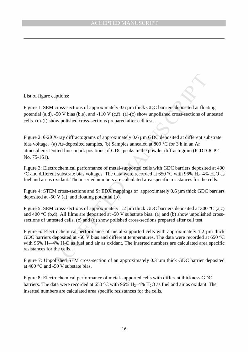
List of figure captions: Figure 1: SEM cross-sections of approximately 0.6 µm thick GDC barriers deposited at floating potential (a,d), -50 V bias (b,e), and -110 V (c,f). (a)-(c) show unpolished cross-sections of untested cells. (c)-(f) show polished cross-sections prepared after cell test.
Figure 2: θ-2θ X-ray diffractograms of approximately 0.6 µm GDC deposited at different substrate bias voltage. (a) As-deposited samples, (b) Samples annealed at 800 °C for 3 h in an Ar atmosphere. Dotted lines mark positions of GDC peaks in the powder diffractogram (ICDD JCP2 No. 75-161).
Figure 3: Electrochemical performance of metal-supported cells with GDC barriers deposited at 400 °C and different substrate bias voltages. The data were recorded at 650 °C with 96% H2–4% H2O as fuel and air as oxidant. The inserted numbers are calculated area specific resistances for the cells. Figure 4: STEM cross-sections and Sr EDX mappings of approximately 0.6 µm thick GDC barriers deposited at -50 V (a) and floating potential (b). Figure 5: SEM cross-sections of approximately 1.2 µm thick GDC barriers deposited at 300 °C (a,c) and 400 °C (b,d). All films are deposited at -50 V substrate bias. (a) and (b) show unpolished cross-sections of untested cells. (c) and (d) show polished cross-sections prepared after cell test. Figure 6: Electrochemical performance of metal-supported cells with approximately 1.2 µm thick GDC barriers deposited at -50 V bias and different temperatures. The data were recorded at 650 °C with 96% H2–4% H2O as fuel and air as oxidant. The inserted numbers are calculated area specific resistances for the cells. Figure 7: Unpolished SEM cross-section of an approximately 0.3 µm thick GDC barrier deposited at 400 °C and -50 V substate bias. Figure 8: Electrochemical performance of metal-supported cells with different thickness GDC barriers. The data were recorded at 650 °C with 96% H2–4% H2O as fuel and air as oxidant. The inserted numbers are calculated area specific resistances for the cells.
MANUSCRIP
T
ACCEPTED
ACCEPTED MANUSCRIPT
Table I: Average out-of-plane grain size and microstrain calculated from the X-ray diffractograms for 0.6µm GDC films deposited at different substrate bias voltage. Calculations have been performed before and after annealing at 800 °C in Ar for 3 hours.
Orientation Average grain size (nm) RMS microstrain (%)
Floating potential
<111> 26.0±1.6 0.4±0.1
<200> 43.8±7.1 0.5±0.1
<220> 19.0±1.2 0.4±0.1
<311> 17.7±1.7 -
-50 V bias
<111> 13.6±2.2 1.6±0.2
<200> 28.0±14 1.4±0.2
<220> 8.6±1.8 1.2±0.2
<311> - -
-110 V bias
<111> 8.2±3.0 1.3±0.7
<200> 27.7±7.5 1.1±0.1
<220> - 2.4±0.8
<311> - -
-50 V, annealed
<111> 31.7±4.1 0.6±0.1
<200> 30.4±4.8 0.6±0.1
<220> 28.1±2.6 0.6±0.05
<311> 21.0±3.6 0.5±0.1
-110 V, annealed
<111> 24.8±4.4 0.8±0.2
<200> 35.4±6.5 0.6±0.1
<220> 19.5±2.6 0.6±0.1
<311> 29.4±6.0 0.6±0.1
MANUSCRIP
T
ACCEPTED
ACCEPTED MANUSCRIPT
MANUSCRIP
T
ACCEPTED
ACCEPTED MANUSCRIPT
MANUSCRIP
T
ACCEPTED
ACCEPTED MANUSCRIPT
MANUSCRIP
T
ACCEPTED
ACCEPTED MANUSCRIPT
MANUSCRIP
T
ACCEPTED
ACCEPTED MANUSCRIPT
MANUSCRIP
T
ACCEPTED
ACCEPTED MANUSCRIPT
MANUSCRIP
T
ACCEPTED
ACCEPTED MANUSCRIPT
MANUSCRIP
T
ACCEPTED
ACCEPTED MANUSCRIPT
MANUSCRIP
T
ACCEPTED
ACCEPTED MANUSCRIPT
• Sputtered gadolinia-doped ceria barriers implemented in metal-based SOFCs. • Sr diffusion along column boundaries in the barrier layer is observed.
• Tuning deposition parameters makes 0.6 µm GDC effectively stop Sr diffusion. • Area specific resistance of 0.34 Ωcm2 is achieved for cells operating at 650 °C.


![Phase stability of AlYB14 sputtered thin filmshenkelmanlab.org/pubs/kolpin09_355006.pdf · AlxYyB14 samples were synthesized by magnetron sputtering within a combinatorial setup [12]](https://img.dokumen.tips/doc/110x75/5e4bb86a8d90841bf1702312/phase-stability-of-alyb14-sputtered-thin-alxyyb14-samples-were-synthesized-by-magnetron.jpg)