Embed Size (px)
Citation preview
May 20, 2004 10:26 WSPC/140-IJMPB 02467
International Journal of Modern Physics BVol. 18, No. 8 (2004) 1083–1118c© World Scientific Publishing Company
MAGNETO-TRANSPORT AND MAGNETO-OPTICAL
PROPERTIES OF FERROMAGNETIC (III,Mn)V
SEMICONDUCTORS: A REVIEW
JAIRO SINOVA∗
Texas A&M University, Physics Department, 4242 TAMU,
College Station, TX 77943-4242, USA
T. JUNGWIRTH
University of Texas at Austin, Physics Department, 1 University Station C1600,
Austin TX 78712-0264, USA
and Institute of Physics ASCR, Cukrovarnicka 10, 162 53
Praha 6, Czech Republic
JOHN CERNE
Depatment of Physics, University at Buffalo, SUNY,
Buffalo, New York 14260, USA
Received 23 February 2003
Rapid developments in material research of metallic ferromagnetic (III,Mn)V semicon-ductors over the past few years have brought a much better understanding of thesecomplex materials. We review here some of the main developments and current under-standing of the bulk properties of these systems within the metallic regime, focusingprincipally on the magneto-transport and magneto-optical properties. Although severaltheoretical approaches are reviewed, the bulk of the review uses the effective Hamilto-nian approach, which has proven useful in describing many of these properties namely in(Ga,Mn)As and (In,Mn)As. The model assumes a ferromagnetic coupling between Mnd-shell local moments mediated by holes in the semiconductor valence band.
Keywords: Diluted magnetic semiconductors; ferromagnetism; magneto-optics; andmagneto-transport.
1. Introduction
The artificial marriage of ferromagnetic and semiconducting properties is one of
the main motivations behind the creation and study of diluted magnetic semicond-
cutors (DMS) focused on (III,Mn)V materials. This effort is being fueled, in large
∗Corresponding author.
1083
May 20, 2004 10:26 WSPC/140-IJMPB 02467
1084 J. Sinova, T. Jungwirth & J. Cerne
part, by the endless demand for technological advances in our society whose global
interdependence in communications and technology is evident throughout our daily
activities. Moore’s law, predicting an exponential growth of computational ability,
is now believed to be in peril and there is a need for a new technological revolution
if the fast pace of technology is to be mantained.
Such a technological revolution will take place if three major goals can be
achieved in the development of ferromagnetic (III,Mn)V materials: (i) room tem-
perature ferromagnetism, (ii) dependence of transport and optical properties on the
magnetic state, and (iii) that the materials mantain their fundamental semiconduct-
ing characteristics, i.e. strong sensitivity to doping, external fields, and light, and
are compatible and integrable with conventional (non-magnetic) micro- and opto-
electronic semiconductor technologies. Since the first observation of ferromagnetism
at low temperatures in the (III,Mn)V semicondcutors in the early nineties,1 steady
progress has been taking place in each of these major fronts. More importantly, over
the last five years, jumpstarted by the discovery of ferromagnetism in (Ga,Mn)As
with ferromagnetic temperatures in excess of 100 K,2 the efforts in this field have
increased dramatically in several coordinated fronts, both experimental and the-
oretical. This rapid research has yielded many advances, prompting the need for
an overall review of at least several fast evolving parts of this scientific effort. In
this article we discuss transport and magento-optical properties of these materials
focusing on the metallic regime and on theoretical approaches based on the effective
Hamiltonian model which have been succesful in obtaining qualitative and quan-
titative understanding of various transport characteristics of these systems. Other
important areas, such as the insulating low-doping regime have been covered by
other reviews.3,4 Furthermore, we will narrow our focus on the most widely studied
and well understood materials, (Ga,Mn)As and (In,Mn)As, only mentioning briefly
some of the current prevailing ideas in regards to the much lesser understood ones
such as the Mn-doped nitrides or phosphides.
As in any review, a preference must be given to the more relevant publications
containing the most recent developments and the ones which have had the largest
impact in understanding these complex materials. Unless the reference section is
equal in length to the actual review, it is impossible to cite every contribution to
this field. To remedy omissions that may have partly originated from the authors’
own work perspective, we refer to a more extended and precise database of pub-
lished and pre-print works maintained within the “Ferromagnetic Semiconductors
Web Project” at http://unix12.fzu.cz/ms. This web page contains a large body of
theoretical and experimental results (that can be obtained in several formats), as
well as the most extended bibliography database linked to diluted magnetic (III,V)
semicondcutors that we are aware of. We encourage the reader in need of a more
detailed bibliography to use this resource.
We also note that a few review articles on other aspects of the physics of DMS,
which we will not discuss extensivelly in this review, have appeared over the past
few years and may help the reader who wants to extend the narrow scope of this

May 20, 2004 10:26 WSPC/140-IJMPB 02467
Magneto-Transport and Magneto-Optical Properties 1085
article. Given however the rapid developments over the past two years alone, the
reader should be warned that these reviews, although excellent, may not suffice
to give the most current experimental developments and theoretical understanding
and justifications. Several extended papers on the physics of ferromagnetism and
proposed mechanisms, some of which we briefly review here, are shown in Refs. 2,
5, 6 and 7. A theoretical review of the widely used phenomenological Zener mean
field model, highly successful in (Ga,Mn)As and (In,Mn)As studies, is presented in
Refs. 8 and 9. A large body of work up to 2001 in density functional first princi-
ples calculations in (III,V) DMS is also available in Ref. 10. Another theoretical
approach based on lattice models and dynamical mean field treatment of disorder,
most successful in the low-doping regime, is reviewed in Ref. 3. The ever important
effects of disorder, omnipresent in these materials, is reviewed in Ref. 4. A gen-
eral discussion behind the technological motivation for DMS has been presented in
Refs. 11, 12, 13, and 14, where optical insulators and magnetoresistance elements
are explored.
We organize the rest of this article as follows: In Section 1.1 we present a short
general overview of DMS from the experimental facts point of view. In Section 2 we
briefly discuss the theoretical model used and its experimental basis to describe the
metallic regime. Section 3 reviews the transport properties of DMS such as diago-
nal resistivity, magneto-resistance anisotropy, and anomalous Hall effect. Section 4
covers the different optical and magneto-optical properties of the systems such as
optical absorption, magnetic-circular diachroism, Raman scattering, and cyclotron
resonance. A short summary and outlook with different open questions is given in
Section 5.
1.1. The basic picture of DMS
The basic idea behind creating these novel ferromagnetic materials is simple: based
on the lower valence of Mn, substituing Mn in a (III,V) semiconductor for the
cations can dope the system with holes; beyond a concentration of 1% there
are enough induced holes to mediate a ferromagnetic coupling between the local
S = 5/2 magnetic moments provided by the strongly localized 3d5 electrons of Mn
and a ferromagnetic ordered state can ensue. This rudamentary but generally cor-
rect picture of ferromagnetism in many (III,Mn)V materials is of course acquired by
piecing together the different experimental results obtained through different char-
acterization techniques of the materials. The simplicity of the model hides within it
a cornucopia of physical effects present in these materials such as metal–insulator
transitions, carrier mediated ferromagnetism, disorder physics, magneto-resistance
effects, magneto-optical effects, intricate coupled magnetization dynamics, post-
growth dependent properties, etc.
In any doped semiconductor, an understanding of its properties must be pre-
ceeded by a study of the doping impurities. Since, in this case, the Mn im-
purity dopants provide the local magnetic moments which are responsible for

May 20, 2004 10:26 WSPC/140-IJMPB 02467
1086 J. Sinova, T. Jungwirth & J. Cerne
ferromagetism and, at the same time, provide the hole carriers which mediate the
exchange coupling between the impurities themselves, understanding the nature of
the impurities and the different states that they induce is even more fundamental
in order to establish a relevant theoretical model.
1.2. Impurities in DMS
Under equilibrium growth conditions, the solubility of Mn in III-V semiconductor
crystals has an upper limit of 0.1%. Beyond this concentration phase separation and
surface segregation take place. To circumvent this problem, low-temperature molec-
ular beam epitaxy (LT-MBE) technique was applied leading to the first successful
growth of InAs and GaAs based DMS.1 The most common and stable position of
Mn in the host semiconductor lattice is on the Ga site.15–19
An important initial question is what is the neutral state of the Ga-
substitutional Mn impurity. Experimentally, through electron paramagnetic res-
onance (EPR) and optical measurements,16,20,21 even for very few percentagea of
Mn the only impurity level observed is the d5-Mn2+ ionized state, indicating that
indeed the strongly localized 3d5 electrons with total spin S = 5/2 are a good
starting point for theoretical models. The corresponding 3d5 plus a weakly bound
hole neutral state is observed experimentally only within a narrow range of Mn
concentrations due to a complete compensation in the low Mn doping regime and
due to the Mott insulator-to-metal transition at high doping. Other candidates
for the Mn neutral impurity such as 3d4 states, important for double-exchange
models to be applicable, are not observed experimentally.16 Furthermore, the itin-
erant holes originating from the Mn acceptor level have also been observed, through
photoemission experiments,22,23 to be associated with the ones of the host semicon-
ductor valence band, i.e. they have As 4p-character, which provides further evidence
for the shallow acceptor nature of the substitutional Mn impurity in GaAs and InAs.
The other impurities present because of the non-equilibrium growth process, As-
antisites and Mn-interstitials, compensate the induced holes and therefore reduce
the free carrier concentration with respect to the substitutional-Mn density. Anneal-
ing procedures, at temeratures slightly lower than growth temperature, have shown
to give a reduction of the amount of compensation.5,24–29 The initial procedure5
has now been modified by different groups24–26,29 and the carrier concentration
can actually be tuned precisedly through resistance-monitored annealing.24 Two
possible mechanism for the reduction of compensation have been considered: ei-
ther the number of As-antisites is reduced through migration of As atoms to their
correct sites, or the Mn-interstitials migrate to the surface or to the substitutional
sites. Early theoretical models assumed the former scenario, however, a recent key
Rutherford backscattering experiment25 has shown that it is the reduction of Mn-
interstitials and their out-diffusion to the surface28 which is responsible for lowering
the amount of compensation.
aLower by an order of magnitude than the concentration marking the metal–insulator transition.

May 20, 2004 10:26 WSPC/140-IJMPB 02467
Magneto-Transport and Magneto-Optical Properties 1087
1.3. Other experimental observations in DMS
Besides the experimental results revealing what is happening in the complicated
annealing process and the nature of the impurities, there are other experimental
observations that provide key clues for understanding of the origins and fundamen-
tal properties of (Ga,Mn)As and (In,Mn)As DMS:
(a) The ferromagnetic behavior of DMS materials is only observed above a critical
doping level of about 1%.5 At lower doping the compensation is almost com-
plete and the mediating carriers needed to exchange-couple the localized Mn
moments are not present and therefore no ferromagnetic ordering occurs.
(b) The carrier-induced ferromagnetic nature of the ordered state has been demon-
strated by field-effect (In,Mn)As experiments30 where the carrier concentration
was tuned by a gate and the corresponding critical temperature was modified
accordingly.
(c) Strain effects, due to the lattice mismatch between the DMS layer and the
substrate, influence the magnetic anisotropy of the ferromagnetic state. It has
been shown that the ferromagnetic easy axis can be along the growth direction
or in the plane depending on whether the strain is tensile or compressive.5,9
Such phenomena are interpreted in terms of well known strain effects in the
spin–orbit coupled valence bands of the host semiconductor.
(d) Both magneto-optical effects, e.g. magnetic circular diachroism (MCD),31 and
resistivity measurements above the critical temperature,32 indicate an anti-
ferromagnetic coupling between the local 3d5 electrons and the valence hole.
This so-called kinetic–exchange interactions originates from the hybridization
between the Mn 3d-orbitals and the neighboring As 4p-orbitals and is much
larger than the pure Coulomb exchange interaction.33
(e) In transport measurements, a large anomalous Hall effect (AHE) (see
Section 3.4) completely dominates the low-field off-diagonal resistance coef-
ficient. The strong intrinsic spin–orbit coupling present in the host semicon-
ductor valence band can account for the measured magnitude and sign of the
AHE.
There are of course many other relevant experiments which are not higlighted
above which must be taken into account. However the interpretation of some or
most of them are still being debated, since they seem to depend critically on the
annealing procedures and can be interpreted in several ways. The above results are
considered to be general and well established and will likely not change in the newly
grown samples as the materials development progresses.
2. Theoretical Models of DMS
The modeling of a collective behavior of interacting electrons is a complicated task
and, in many instances, must be guided by experimental evidence of the low energy
degrees of freedom in order to obtain a correct minimal model which will capture

May 20, 2004 10:26 WSPC/140-IJMPB 02467
1088 J. Sinova, T. Jungwirth & J. Cerne
the observed effects and will make useful predictions. With this in mind, there
are typically three approaches, somewhat complementary, used to describe DMS
systems:
• first principles density-functional theory (DFT) and microscopic tight-binding
models,
• effective Hamiltonian models, and
• lattice models.
DFT is an important tool for studying the microscopic origin of ferromag-
netism through calculations of electronic, magnetic, and structural ground-state
properties.10 A local-density-approximation (LDA) of the DFT, combined with
disorder-averaging coherent-potential approximation (CPA) or supercell approach,
has been used successfully to address physical parameters of (III,Mn)V DMS that
are derived from total-energy calculations, such as the lattice constants,34 and for-
mation and binding energies of various defects.18,19 However, in Mn-doped DMS,
LDA fails to account for strong correlations that suppress fluctuations in the num-
ber of electrons in the d-shell. As a result, the energy splitting between the occupied
and empty d-states is underestimated which leads to an unrealistically large d-state
local DOS near the top of the valence band, and to an overestimate of the strength
of the sp–d hybridization.10,35 This shortcomings have been corrected recently by
LDA+U and self-interaction corrected LDA schemes, which account for correlations
among Mn 3d electrons, and have been used to obtain more realistic energy spectra
and show agreement with the experimental observation that the valence holes have
mostly As 4p-character.36
A practical approach, that circumvents some of the complexities of this
strongly-correlated many-body problem is the microscopic tight-binding (TB) band-
structure theory. Within the model, local changes of the crystal potential at Mn
and other impurity sites are represented by shifted atomic levels. A proper param-
eterization of these shifts, with the Hubbard correlation potential that favors single
occupancy of the localized d-orbitals, and the Hund potential forcing the five d-
orbital spins to align, and of the hopping amplitudes between neighboring atoms
provides the correct band gap for the host III-V semiconductor and an appropriate
exchange splitting of the Mn d-levels. The TB model is a semi-phenomenological
theory, however, it shares the virtue with first principles approaches of treating
disorder microscopically. The decoherence of Bloch quasiparticle states or effects of
doping and disorder on the strength of the sp–d exchange coupling and effective
Mn–Mn interaction are among the problems that have been analyzed using this
tool.37–39
In the metallic regime, where the largest critical ferromagnetic temperatures
are achieved (for doping levels above 1.5%40), semi-phenomenological models that
are built on Bloch states for the band quasiparticles, rather than localized basis
states appropriate for the localized regime,41 provide the natural starting point for
a model Hamiltonian which reproduces many of the observed experimental effects.
Recognizing that the length scales associated with holes in the DMS compounds

May 20, 2004 10:26 WSPC/140-IJMPB 02467
Magneto-Transport and Magneto-Optical Properties 1089
are still long enough, a k · p envelope function description of the semiconductor
valence bands is appropriate. Since for many properties, e.g. anomalous Hall effect
and magnetic anisotropy, it is necessary to incorporate intrinsic spin–orbit coupling
in a realistic way, the six-band (or multiple-band, in general) Kohn–Luttinger (KL)
k · p Hamiltonian that includes the spin–orbit split-off bands is desirable.9,42 The
approximation of using the KL Hamiltonian to describe the free holes is based
primarily in the shallow acceptor picture demonstrated by the experiments15–17 in
(Ga,Mn)As and (In,Mn)As and must be re-examined for any other DMS materials
that this model is applied to.
Besides the KL Hamiltonian parameters of the host III–V compound which
have long been established,43 the phenomenological part of the strategy follows
from asserting, rather than deriving, the localized nature of the Mn d-orbital mo-
ments and from parameterizing the sp–d hybridization by an effective exchange
constant Jpd. The localization assumption is again verified by electron resonance
experiments15–17 and the value of Jpd is obtained from resistivity measurements in
the paramagnetic regime32 and MCD measurements.31 Hence, the effective Hamil-
tonian considered within this model is
H = HKL + Jpd
∑
I
SI · s(r)δ(r −RI) + Hdis , (1)
where HKL is the six-band (multiple-band) Kohn–Luttinger (KL) k · p
Hamiltonian,8,9 the second term is the short-range antiferromagnetic kinetic–
exchange interaction between local spin SI at site RI and the itinerant hole spin
(a finite range can be incorporated in more realistic models), and Hdis is the scalar
scattering potential representing the difference between a valence band electron on
a host site and a valence band electron on a Mn site and the screened Coulomb
interaction of the itinerant electrons with the ionized impurities.
Several approximations can be used to vastly simplify the above model, namely,
the virtual crystal approximation (replacing the spatial dependence of the local
Mn moments by a constant average) and the mean field theory description.8,9 In
the metallic regime, the disorder can be treated by a Born approximation or by
more sophisticated, exact-diagonalization or Monte-Carlo methods.44–48 The ef-
fective Hamiltonian in Eq. (1) allows us to use standard electron-gas theory tools
to account for hole–hole Coulomb interactions. This envelope function approxi-
mation model is also suitable for studying magnetic semiconductor heterostruc-
tures, like superlattices, quantum wells and digitally doped layers.49 The validity
of such semi-phenomenological Hamiltonian, which does not contain any free pa-
rameters, must be confirmed ultimately by experiments. Its accurate description
of many thermodynamic and transport properties of metallic (Ga,Mn)As samples,
such as the measured transition temperature,50,51 the anomalous Hall effect,52,53
the anisotropic magnetoresistance,44,52 the magneto-crystalline anisotropy,42,54 the
spin-stiffness,54 the ferromagnetic domain wall widths,55 the magnetic dynamic
damping coefficients,56 and the magneto-optical properties,9,45,57 has proven the
merit of this effective Hamiltonian approach.
May 20, 2004 10:26 WSPC/140-IJMPB 02467
1090 J. Sinova, T. Jungwirth & J. Cerne
One has to keep in mind, however, that as any semi-phenomenological model it
may fail to capture the correct physics that leads to the ferromagnetic phase in some
materials or in a certain range of parameter values. Such models can only be ver-
ified by careful comparison with experiments and tested through their predictions
and agreement with experimetnts. For example, Mn-doped nitride and phosphide
compounds or insulating DMS samples with low concentration of Mn ions require a
theoretical description that goes beyond the picture of the host band quasiparticles
that are weakly hybridized with the localized Mn d-electrons. Particularly nitrates
are not believed to be well modeled by this semi-phenomenological Hamiltonian
since Mn is a deep acceptors in this case and and charge fluctuations on the Mn
d-levels may play important role.
There has also been theoretical work on (III,Mn)V DMS materials based on
a still simpler model where holes are assumed to hop only between Mn acceptor
sites, where they interact with the Mn moments via phenomenological exchange
interactions.3,58 These models have the advantage of approaching the physics of
the insulating dilute Mn limit, and can also be adapted to include the holes that
are localized on other ionized defects besides the Mn acceptors through dynamical
mean field (or CPA) techniques. The free-parameter nature of this phenomeno-
logical approach and their oversimplified eletronic structure allows one to make
only qualitative predictions, however, and the models are also not appropriate for
studying the high Tc metallic samples.
3. Transport Properties of DMS Systems
The different transport coefficients of DMS and their magnetic, temperature, and
material composition dependance have been the most important and widely used
characterization tools of DMS. Besides the diagonal resistivity which indicates
metal–insulator transitions and possible critical behavior at the ferromagnetic tran-
sition temperature, other material transport properties such as anisotropic magne-
toresistance, anomalous and ordinary Hall effect, and giant magnetoresistance have
been used to both characterize and test the different theoretical models of DMS ma-
terials. In this section we consider the diagonal conductivity general features, how
the exchange coupling between the localized moments and free carriers is extracted
within the paramagnetic regime, the doping and carrier concentration conductiv-
ity dependency at low temperatures, the anisotropic magnetoresistance, and the
anomalous Hall effect. Throughout, we will focus on the comparison of theoretical
models (mainly the semi-phenomenological effective Hamiltonian model relevant to
the metallic regime) to the different experimental observations.
3.1. General features of resistivity in DMS
DMS materials exhibit an insulating or metallic behavior (defined by the resistivity
in the limit of zero temperature) depending on its doping level and post-growth
annealing procedures. In As-grown samples, metallic behavior is typically observed
May 20, 2004 10:26 WSPC/140-IJMPB 02467
Magneto-Transport and Magneto-Optical Properties 1091
for a range of 2–5% Mn doping and an insulating behavior outside than this range.59
In addition to this metal–insulator quantum transition, the resistivity as a function
of temperature typically exhibits a peak or shoulder near the ferromagnetic transi-
tion temperature for both insulating (peak) and metallic (shoulder) samples.60–62
The non-monotonic behavior near Tc is typically associated with critical-scattering
but so far no theory has been developed which explains such behavior in a qual-
itative or quantitative way. Typically the Fisher–Langer theory of correlated fluc-
tuations is invoked. However, it predicts an infinite derivative of the resistivity at
Tc, which is clearly not the case in any studied (Ga,Mn)As DMS sample. There
exists also a drastic reduction of the resistivity upon annealing, associated with
the increase of the carrier concentration and to a lesser extent a reduction of the
disorder scatterers.24,59–62 The on-set of the metal–insulator transition at 1.5% Mn
doping is close to the Mott insulator limit of a doped semiconductor similar to Si:P
and the optimally annealed samples remain metallic throughout the whole range of
Mn concentrations above 1.5%.40
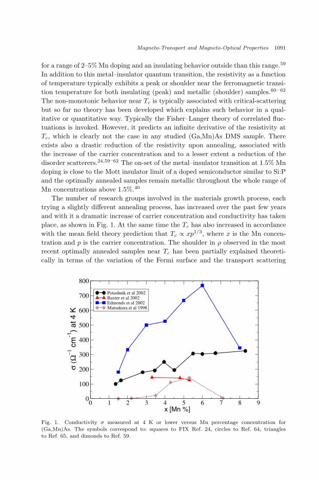
The number of research groups involved in the materials growth process, each
trying a slightly different annealing process, has increased over the past few years
and with it a dramatic increase of carrier concentration and conductivity has taken
place, as shown in Fig. 1. At the same time the Tc has also increased in accordance
with the mean field theory prediction that Tc ∝ xp1/3, where x is the Mn concen-
tration and p is the carrier concentration. The shoulder in ρ observed in the most
recent optimally annealed samples near Tc has been partially explained theoreti-
cally in terms of the variation of the Fermi surface and the transport scattering
0 1 2 3 4 5 6 7 8 9
x [Mn %]
0
100
200
300
400
500
600
700
800
σ (
Ω−
1 c
m-1
) a
t 4
K
Potashnik et al 2002
Baxter et al 2002
Edmonds et al 2002
Matsukura et al 1998
Fig. 1. Conductivity σ measured at 4 K or lower versus Mn percentage concentration for(Ga,Mn)As. The symbols correspond to: squares to FIX Ref. 24, circles to Ref. 64, trianglesto Ref. 65, and dimonds to Ref. 59.
May 20, 2004 10:26 WSPC/140-IJMPB 02467
1092 J. Sinova, T. Jungwirth & J. Cerne
time associated with the ferromagnetic to paramagnetic phase transition.63 How-
ever, there is no model at present that reproduces fully the behavior observed in
ρ as a function of temperature near Tc in the metallic regime for most samples.
There has also been theoretical progress in understanding of the low temperature
regime44 (Section 3.3) and the role of scattering off magnetic impurities in the high
temperature paramagnetic regime (Section 3.2).32,59
3.2. Scattering off the kinetic–exchange potential in the
paramagnetic regime
The contribution from magnetic impurities to the resistivity behavior observed
above Tc can be understood assuming scattering from the kinetic–exchange term
in the Hamiltonian
Hk−e = Jpd
∑
I
δ(r −RI)SI · s . (2)
The corresponding contribution to the resistivity is given by33,32
ρs = 2π2 kF
pe2(m∗)2J2
pd
h3NMn[2χ⊥(T,B) + χ‖(T,B)] , (3)
where kF is the carrier Fermi wave vector, h is the Planck constant, NMn the
density of substitutional Mn, m∗ is the effective mass of the carrier, and e is the
electron charge. Here, χ⊥ = M/B and χII = ∂M/∂B are the transverse and
longitudinal magnetic susceptibilities. Using transport data, the susceptibility can
be determined from the Hall resistivity due to the dominant contribution from the
anomalous Hall effect which is proportional to the magnetization.32 The analysis
of magnetoresistance data above Tc gives
Jpd = 55 ± 10 meV nm3 .
This result is in agreement with optical MCD data (see Section 4). We also note that
the initial expression used to analyze the magnetoresistance data, which replaces
the susceptibility factor by [S(S + 1) − 〈S〉2], neglected the correlations between
neighboring Mn spins and overestimated Jpd by a factor of 3, in disagreement then
with the MCD measurement of Jpd.59
3.3. Boltzman transport theory of the zero temperature
conductivity in DMS
The zero temperature conductivity of metallic DMS samples can be obtained from
the effective Hamiltonian [Eq. (1)] and by accounting for disorder scattering per-
turbatively. The valence band holes interact with randomly located spins of substi-
tutional Mn impurities via the kinetic–exchange interaction, and with randomly lo-
cated ionized defects and each other via Coulomb interactions. At zeroth order, the
interactions are replaced by their spatial averages, so that the Coulomb interaction

May 20, 2004 10:26 WSPC/140-IJMPB 02467
Magneto-Transport and Magneto-Optical Properties 1093
vanishes and hole quasiparticles interact with a spatially constant kinetic–exchange
field. The corresponding mean-field Hamiltonian for the itinerant holes reads
H0 = HKL + JpdNMnSΩ · s , (4)
where Ω is the orientation of fully polarized substitutional Mn local moments and s
is the envelope-function hole spin operator.42 Using the eigenstates of the Hamilto-
nian in Eq. (4), the first order Born approximation of the elastic scattering rate, and
the relaxation-time-approximation solution to the semiclassical Boltzmann equa-
tion, the diagonal DC conductivity tensor along one of the cube edges of the host
lattice can be written as:44
σαα =e2
~V
∑
n,k
1
~Γn,k
(∂En,k
∂kα
)2
δ(EF −En,k) , (5)
where Γn,k is the quasiparticle elastic scattering rate, n and k are the band and
wavevector indices, En,k are the eigenstates of the Hamiltonian (4), and EF is the
Fermi energy.
The Born approximation estimate of the transport weighted scattering rate from
substitutional Mn impurities is given by:
ΓMnn,k =
2π
~NMn
∑
n′
∫dk′
(2π)3|Mk,k′
n,n′ |2δ(En,k −En′k′)(1 − cos θk,k′) , (6)
with the scattering matrix element,
Mk,k′
n,n′ = JpdS〈znk|Ω · s|zn′k′〉 − e2
εhostε0(|k − k′|2 + q2TF)〈znk|zn′k′〉 . (7)
Here εhost is the host semiconductor dielectric constant, |znk〉 is the six-component
(multi-component) envelope-function eigenspinor of the unperturbed Hamiltonian
(4), and the Thomas–Fermi screening wavevector
qTF =√e2DOS(EF)/(εhostε0) ,
where DOS(EF) is the density of states at the Fermi energy.44 This model incorpo-
rates the fact that the transport properties of these materials are not solely deter-
mined by the scattering from substitutional Mn impurities and allows explicitly for
scattering from compensating defects, which have been seen to play a key role in the
resistivity through the post-growth annealing as discussed earlier.5,24–29 As-antisite
defects are non-magnetic double-donors and contribute to scattering through a
screened charge Z = 2 Coulomb potential. The double-donor Mn interstitials24,27
are unlikely to be magnetically ordered and can also be modeled as a Z = 2 screened
Coulomb potential.19
Assuming a parabolic-band disperssion for majority heavy-hole states the
kinetic–exchange scattering contribution to the scattering rate can be estimated
by
Γpd = (NMn)J2pdS
2m∗√
2m∗EF/(4π~4) .

May 20, 2004 10:26 WSPC/140-IJMPB 02467
1094 J. Sinova, T. Jungwirth & J. Cerne
The Mn and As-antisite Coulomb scattering leads to scattering rate ΓC given by the
Brooks–Herring formula.44 For (Ga,Mn)As, taking a heavy-hole effective massm∗ =
0.5me, p = 0.4 nm−3 and Mn doping x = 5%, these estimates give ~Γpd ∼ 20 meV
and ~ΓC ∼ 150 meV. A full numerical six-band calculations is consistent with these
estimates, and predicts that the Coulomb contribution to the elastic scattering rate
is several times larger than the kinetic–exchange contribution for typical chemical
compositions. Note that these estimates give an immediate check on the assumption
of the theory itself, since even in the heavily doped and compensated (Ga,Mn)As
DMS, the lifetime broadening of the quasiparticle (~Γ) is smaller than the valence
band spin–orbit coupling strength (∆so = 341 meV) and the typical Fermi energy.
Figure 2 shows σxx, calculated numerically using the six-band Kohn–Luttinger
model and Eqs. (5) and (6), for a fully strained Mn0.06Ga0.94As sample. The
substrate–DMS lattice mismatch, e0 ≡ (asub − aDMS)/aDMS , is between −0.002
and −0.003 in this case.2,66,65 The absolute conductivities predicted by this model
are reasonably consistent with experiment.24,64,65 The disagreement for lower Mn
concentrations (x < 4%) of the theoretical conductivities is most likely due to
some combination of inaccuracy in the scattering amplitude estimates, unaccounted
sources of scattering, and, especially at small x, coherent scattering effects that
eventually lead to localization observed as an upturn in ρ at the lowest tempera-
tures.
In addition to the AHE (Section 3.4), strong spin–orbit coupling in the semi-
conductor valence band leads also to anisotropies in the longitudinal transport
0.1 0.2 0.3 0.4 0.5 0.6
p (nm-3
)
0
500
1000
1500
2000
σxx (
Ω-1
cm
-1)
total
majority heavy-hole
minority heavy-hole
majority light-hole
minority light-hole
Fig. 2. Conductivity for measuring current and magnetization directed along the x-axis in theplane of the (Ga,Mn)As film as a function of the total hole density. These results were obtainedfor a GaAs semiconductor host doped with 6% Mn. For typical hole densities the current is carriedmostly by the majority heavy-holes.

May 20, 2004 10:26 WSPC/140-IJMPB 02467
Magneto-Transport and Magneto-Optical Properties 1095
0 2 4 6 8x (%)
-20
-15
-10
-5
0
5A
MR
op (%
)theory (As-antisites)
theory (Mn-interstitials)
experiment
0 2 4 6 8x (%)
-15
-10
-5
0
AM
Rip
(%
)
Fig. 3. Experimental (filled symbols) AMR coefficients and theoretical data obtained assumingAs-antisite compensation (open symbols) and Mn-interstitial compensation (semi-filled symbols)of AMRop and AMRip. (After Ref. 52.)
coefficients. In particular, when the magnetization M is rotated by applying an
external magnetic field stronger than the magneto-crystalline anisotropy field, the
in-plane conductivity changes.65,67 Figure 3 shows the theoretical and experimental
AMR coefficients,
AMRop = [σxx(M ‖ z) − σxx(M ‖ x)]/σxx(M ‖ x)
and
AMRip = [σxx(M ‖ y) − σxx(M ‖ x)]/σxx(M ‖ x) ,
for the seven (Ga,Mn)As samples.24,52,65 Here z is the growth direction. Results
of the two disordered system models, one assuming As-antisite and the other one
Mn-interstitial compensation, are plotted in Fig. 3. As in the AHE case, the the-
oretical results are able to account semi-quantitatively for the AMR effects in the
(Ga,Mn)As DMS, with somewhat better agreement obtained for the model that
assumes Mn-interstitial compensation, which confirms indirectly the experimental
finding that the compensating defects are dominated by Mn-interstitials.27 Note
that although the magnitude of the conductivities tend to be overestimated, the
magnetotransport effects are relatively insensitive to scattering strength, reflecting
instead the strong spin–orbit coupling in the valence band of the host semiconductor
as compared to the Fermi energy.52
A large anisotropic magnetoresistance effect is observed experimentally also in
the off-diagonal symmetric conductivity component (σxy = +σyx) when magneti-
zation direction changes from parallel to x- or y-axis, where σxy = σyx = 0, to

May 20, 2004 10:26 WSPC/140-IJMPB 02467
1096 J. Sinova, T. Jungwirth & J. Cerne
a general orientation in the x–y plane tilted from the two transport measurement
axes, where σxy = σyx 6= 0.68 The effect is sometimes called a “planar Hall effect”
but we emphasize that the true Hall response requires the symmetry σxy = −σyx.
The anomalous contribution to this asymmetric off-diagonal transport coefficient is
discussed in the following section.
3.4. Hall resistivity and the anomalous Hall effect
One of the most important characterization tools of magnetic materials is the
anomalous Hall effect.69 The Hall resistance RHall ≡ ρxy/d of a magnetic thin
film is empirically observed to contain two distinct contributions. The first arises
from the normal Hall effect contribution which is proportional to the applied mag-
netic field, H ; and the second, called the anomalous Hall contribution, is observed
to be proportional to the magnetization:70
RHall = R0H +RSM , (8)
where M is the magnetization perpendicular to the thin film surface, and R0 and
RS are the ordinary and anomalous Hall coefficients respectively. The ordinary
Hall effect is due to the Lorentz force on the carriers and is used to measure the
concentration and nature of the free carriers since R0 is linearly proportional to the
free carrier density and its sign determines whether they are electrons or holes. On
the other hand, the anomalous Hall effect is a direct consequence of the presence of
spin–orbit coupling in the system. In many instances, such as the DMS for example,
the anomalous contribution is much greater than the ordinary Hall effect, making
the carrier density hard to measure since large magnetic field must be used to
extract the linearity in the field of the Hall resistance. However, the overwhelming
of the Hall coefficient by RS allows one to utilize the anomalous Hall effect as
an indirect measure of the magnetization. Empirically RS is observed to depend
quadratically or linearly on the diagonal resistivity ρ, depending on the material.
For example, for the case of Fe (Ref. 70) and GaMnAs (Ref. 66), the dependance
on the resistivity is quadratic. These two resistivity dependencies of RS correspond
to different possible origins of the anomalous Hall effect which we discuss below.
However, in spite of its wide use, it is surprising how much confusion has followed
over the past six decades. Although much progress has taken place over the past
few years with the creation and study of new materials, no single theory has been
able to systematically and convincingly explain the constant puzzle of side-jump
versus intrinsic mechanisms (see below) although it is at present a feasable but
challenging undertaking.
3.4.1. The embroiled history of the anomalous Hall effect
Before discussing the theoretical description of the anomalous Hall effect in DMS,
it is appropriate to make an excursion to the history of the field in order to under-
stand clearly the origin of the controversies and the strength and weaknesses of the

May 20, 2004 10:26 WSPC/140-IJMPB 02467
Magneto-Transport and Magneto-Optical Properties 1097
different arguments put forth by different researchers. Often such summaries are
done in two or three sentences giving an oversimplified view of the controversy and
the different points of view, some of which have been challenged in later literature
but still remain in the general folklore.
The first detailed theoretical consideration of the anomalous Hall effect was
given by Karplus and Luttinger,71 where they considered the problem from a per-
turbative point of view (with respect to an applied electric field) and obtained
a contribution to the Hall conductivity in systems with spin–orbit coupled Bloch
states given by the expression (Eqs. (2.16) and (2.17) in Ref. 71)
σxy = −2e2
~V
∑
n,k
nF(Ek,n)Im
⟨∂un,k
∂ky
∣∣∣∣∂un,k
∂ky
⟩, (9)
where nF is the Fermi occupation number of the Bloch state |un,k〉. This expression
is obtained by ignoring impurity scattering (i.e. clean limit) and can also be obtained
from the Kubo linear response theory in this clean limit (see below). One of its
immediate successes was the prediction that RS is proportional to ρ2 in agreement
with many materials, Fe being the primary example. Immediately after Karplus and
Luttinger’s pioneering work, Smit72 considered the problem of impurity scattering
within a Boltzman formalism using a model Hamiltonian of an electron gas, i.e. plain
waves, without intrinsic spin–orbit coupling and a scattering potential containing
both direct and spin–orbit coupled terms:
H =p2
2m+ V (r) +
1
2m2c2r
∂V (r)
∂rSzLz (10)
where the impurity potential is V (r) = 0 for r > R and V (r) = V0 for r < R.
Within the Boltzman formalism, he obtained a second type of contribution to the
Hall conductivity due to the asymmetric scattering from impurities originating from
the spin–orbit coupling term. This so-called skew-scattering mechanism predicts,
in contrast to the intrinsic effect found by Karplus and Luttinger, that RS ∝ ρ
(i.e. density of scatterers) and dependence on the type and range of the scattering
potential. It was also noted that the magnitude of the effect within such simplified
model was many orders of magnitude lower than the observed magnitude of the
AHE but, as it was shown later, the origin of this deficiency is the lack of intrinsic
spin–orbit coupling present in the crystal Bloch states. However, Smit also critiziced
Karplus and Luttinger’s result claiming the intrinsic contribution vanishes. Such
claim (see below) is now understood to be unjustified but has remained lingering
in the AHE literature, generating much confusion.
Karplus and Luttinger71 did not consider impurity scattering, hence omitted
the skew-scattering contribution in their calculation. To remedy this, Kohn and
Luttinger73 developed a consistent (and somewhat cumbersome) treatment to ob-
tain the transport coefficients in the presence of spin–orbit coupling and disorder
scattering based on a density matrix expansion. Such approach is equivalent to
the Kubo linear response formalism but technically more difficult when applied to

May 20, 2004 10:26 WSPC/140-IJMPB 02467
1098 J. Sinova, T. Jungwirth & J. Cerne
real physical systems. Within this formalism the expansion is done to first order
in spin-orbit coupling and impurity scattering strength. They obtained, besides the
previous Karplus and Luttinger result (Eq. (135) in Ref. 73, however note that it
has the wrong sign later corrected in Ref. 74), formal expressions for additional con-
tributions due to impurity scattering. Applying this formalism to a model with un-
correlated impurity potential and small scattering strength, Luttinger74 obtained,
besides the Smit’s skew-scattering term, the same final expression as Karplus and
Luttinger but with the opposite sign (Eq. (3.26) in Ref. 74). Somehow, in addition
to the intrinsic Karplus and Luttinger term, there seemed to be an additional con-
tribution from scattering in the high mobility limit giving a contribution identical
to the intrinsic one but with a factor of −2 in front of it, hence the flip of sign
of the final expression. No explanation was given of why such a scattering con-
tribution does not depend in any way on the scattering potential but simply on
the electronic structure of the system. However, Luttinger74 showed unequivocally
that the cancelation argued by Smit does not take place. In a slightly different for-
malism Adams and Blouht75 agreed with Luttinger’s results and pointed out that
Smit’s error occurs from an inconsistency involving a change of representation of
his density matrix when calculating the current.
A few years later Berger76 made his first contribution to the problem introduc-
ing the idea (contained within Luttinger’s formalism) of the side-jump scattering
mechanism. He considered the problem of wave-packet scattering off an impurity
potential as in Eq. (10), showing that in addition to skew scattering there exists a
side-step type of scattering. This so-called side-jump, as in the Luttinger formalism,
was independent of the scattering potential, leaving one with the strange notion that
an extrinsic scattering mechanism resulted in an intrinsic property. After putting
this contribution in a Boltzman type formalism he obtained a result which was four
orders of magnitde lower than the Karplus and Luttinger intrinsic result. He then
argued that the intrinsic spin–orbit coulping of the system increases this side-jump
scattering by such factor. In his case the sign of the effect is not directly consid-
ered and his result, as already mentioned, is independent of the scattering potential
itself. A similar type of formalism was put forth by Lyo and Holstein77 claiming
similar results but ignoring, for some unknown reasons, intrinsic non-vanishing con-
tributions of Karplus and Luttinger.
It is then that Leroux-Hugon and Ghazali78 pointed out the resolution of the
missing order of magnitude of the skew-scattering. By looking simply at scattering
of Bloch electrons from ionized impurities Vion(r) alone and going to second order in
the Born approximation within the collision term of the Boltzman transport theory,
they obtained a skew-scattering contribution with a much higher magnitude than
that coming from the spin–orbit coupling of the impurities themselves. Hence, it
became evident that it is the presence of intrinsic spin–orbit coupling through
the crystal potential which is ultimately responsible for the magnitude of all the
anomalous Hall effect contributions observed and a system with weak or no intrinsic
spin–orbit coupling will not exhibit a detectable contribution to the RHall.
May 20, 2004 10:26 WSPC/140-IJMPB 02467
Magneto-Transport and Magneto-Optical Properties 1099
To elucidate this confusing and farraginous atmosphere, Nozieres and Lewiner,79
following the formalism introduced by Fivaz80 in terms of effective Hamiltonians of
semiconductors, developed a theory applicable to narrow gap semiconductors equiv-
alent to Luttinger’s74 but with the final result being more physically transparent.
Going to linear order in impurity scattering and spin–orbit coupling and combining
them with a Boltzamn type of approach, they obtained different contributions to
the Hall current and different behavior when considering opposite orders of limits
of ω → 0 and τ → ∞, where ω is the frequency of the applied electric field and τ is
the quasiparticle lifetime (see Table 1 and Eqs. (59), (60a), and (60b) in Ref. 79).
Besides the skew scattering contribution which depends on the type of scattering
potential, in the limit ωτ 1 (τ → ∞ first), considered by some authors to be
the weak scattering limit (see Refs. 81 and 82), the result is that of Karplus and
Luttinger.71 On the other hand, for ωτ 1 (ω → 0 first), the opposite sign expres-
sion of Luttinger74 is recovered. One must note however that this result seems to
be very specific to the model (single band) and to the meaning of the limit τ → ∞as admitted by the authors themselves.74,79
After this Berger and Smit exchanged salvos in a series of confusing
comments83–86 in which Smit’s old argument, that there is no such a thing as
side-jump or intrinsic contribution, seems to have been finally put to rest. It was
after this that Chazalviel,81 using the results of Nozieres–Lewier–Luttinger74,79
and Leroux-Hugon and Ghazalis,78 attempted to compare phenomenologically the
AHE theory to the n-InSb and n-Ge experimental data with some success. Within
such models, the relative importance of the side-jump/intrinsic contribution σsj/int
aH
(which are the same magnitude but of opposite sign depending on the limits79,81,82)
to the skew-scattering contribution σskaH depends on the nature of the scatterers
(only through the skew-scattering dependence). For scattering from ionized impu-
rities one has78,81
∣∣∣∣∣σ
sj/int
aH
σskaH
∣∣∣∣∣ =cN
prskFl, (11)
with N/p being the ratio of the total number of ionized impurities and carrier
density, rs is the average distance between carriers in units of Bohr radious, l is
the mean free path, and c ∼ 10, varying slightly with scattering length. For short
range scattering potential considered by Luttinger74 and Nozieres and Lewiner,79
V (r) = V0δ(r − ri):∣∣∣∣∣σ
sj/int
aH
σskaH
∣∣∣∣∣ =3
π|V0|D(EF)kFl, (12)
where D(EF) is the density of states at the Fermi energy and kF is the Fermi wave-
vector. These estimates can be a useful first guess at which mechanism dominates
in different materials but one must keep in mind the simplicity of the models used
to estimate such ratio.

May 20, 2004 10:26 WSPC/140-IJMPB 02467
1100 J. Sinova, T. Jungwirth & J. Cerne
In spite of the theory being incomplete, and in some cases self-contradictory and
puzzling, the theoretical developments remained somewhat dormant until recent
interest in new ferromagnetic and spintronic materials. These emerging fields have
demonstrated the need for a better theoretical understanding of the AHE which
has constantly been used to characterize ferromagnetic materials.
We emphasize that there is, at this stage, no controversy regarding the skew-
scattering contribution. In most materials such contribution, although present, is
minor and in most ferromagnetic materials the quadratic dependence of RS is ob-
served even at the lowest temperatures. However, if somehow, one could artificially
turn down ρ one would eventually reach a regime where such contribution is dom-
inant, a fact which very few people dispute since the origin of such contribution is
rather transparent and reassuringly extrinsic in nature. However, the flip of sign of
the expressions derived by Luttinger74 and Nozieres and Leweir79 within the simple
one band model in the different order of limits of ωτ , remains quite disturbing and
a source of continuous debates. After all, these results are only obtained in a limit
where, supposedly, the skew scattering would always dominate. As we will see be-
low, it seems that in many materials experimental comparisons, the ultimate test
of the validity of any theory, are more consistent with the intrinsic Karplus and
Luttinger71 contribution than the reversed sign one of Luttinger;74 the sign of the
effect being a simple thing to check.
A possible resolution to the problem would be to perform the Hall conductivity
calculation within the Kubo linear response formalism, treating disorder and spin–
orbit coupling on an equal footing. This can be achieved by starting from the Dirac
representation and taking the weak relativistic limit after treating disorder in the
usual fashion. In this way, any spin–orbit coupling contribution comes naturally
from the Dirac representation and therefore is automatically taken into account.
On the other hand, if one starts from the Pauli Hamiltonian, an immediate question
arises: which vertex corrections capture the different contributions to the anoma-
lous Hall effect? Such an approach was taken recently by Crepieux, Dugaev and
Bruno.87–89 The work considers, however, a free electron gas model rather than
a crystaline environment, hence ignoring the intrinsic spin–orbit coupling effects.
In spite of this simplification, the authors obtained many useful findings. They
were able to pinpoint which diagrams correspond to the skew and the side-jump
scattering in the Pauli Hamiltonian by identifying them from the corresponding
ones arising naturally from the Dirac formalism. Notably, these diagrams within
the Pauli Hamiltonian, are not the standard ones that one would take into account
naturally. Their main result, Eqs. (50) and (51) in Refs. 87 and 89, is in reasonable
agreement with Berger’s simpler treatment of this free electron gas problem.
Taking into consideration the confusion generated by the possible relevance of
the side-jump scattering mechanism, several researchers have chosen to focus in-
stead on the original intrinsic contribution to the AHE proposed by Karplus and
Luttinger71 and ignore impurity scattering all together or simply include its effects
through the Born approximation which introduces a finite quasiparticle lifetime.

May 20, 2004 10:26 WSPC/140-IJMPB 02467
Magneto-Transport and Magneto-Optical Properties 1101
In DMS, e.g. this approach is partly motivated by the strong intrinsic spin–orbit
coupling in the host valence bands that makes much of the above theoretical discus-
sions inapplicable since they relied on the perturbation treatment of the spin–orbit
coupling. One of the main attraction of the intrinsic AHE theory is the ability to do
calculations in models with realistic electronic band-structures. This approach has
been used, e.g. to analyze the AHE in layered 2D ferromagnets such as SrRuO3,
in pyrochlore ferromagnets,90–93 in the collosal magnetoresistance manganites,94
in Fe,95 in DMS,53 and as a natural starting point to address infrared magneto-
optical effects such as the Kerr and Faraday effects57 (see Section 5). The applica-
tion of this approach to these different materials and their successful comparison
to experiments52,53,66,90–92,95,96 is perhaps the most pogniant criticism to the old
theories regarding the side-jump scattering as fundamental.
3.4.2. Anomalous Hall effect in DMS
The anomalous Hall effect in DMS has been one of the most fundamental char-
acterization tools since it is the simples way of detecting the ferromagnetic state
of the system at a given temperature. The original discovery of ferromagnetism in
(III,Mn)V seminconductors was established by measuring the AHE in both the high
and low temperature regimes.1 The comparison with remenant magnetization mea-
surements using a SQUID magnetometer confirmed, e.g., that AHE measurement
can be used to determine ferromagnetic critical temperature.1
Recently Jungwirth, Niu, and MacDonald53 reintroduced the original Karplus
and Luttinger Eq. (9), pointing out that the intrinsic contribution to the AHE is
proportional to the Berry phase acquired by a quasiparticle wave function upon
traversing closed path on the spin-split Fermi surface. They applied the theory to
metallic (III,Mn)V materials using both the 4-band and 6-band k · p description
of the valence band electronic structure42 and obtained results in a quantitative
agreement with the experimental data in (Ga,Mn)As and (In,Mn)As DMS. In DMS
systems, the estimate given in Eq. (11) gives a ratio of intrinsic to skew scattering
contribution of the order of 50, hence the intrinsic contribution in these systems is
likely to dominate.82 Consistently, Edmonds et al.96 found that in metallic DMS
systems Rs ∝ ρ2. In a follow up work52 a more careful comparison of the theory,
reformulated within the Kubo formalism, was done in order to account for finite
quasiparticle lifetime effects important only for quantitative but not qualitative
comparison with the experimental data. Within the Kubo formalism the DC Hall
conductivity for non-interacting quasiparticles is given by
σxy =ie2~
m2
∫dk
(2π)3
∑
n6=n′
fn′,k − fn,k
Enk −En′k
〈nk|px|n′k〉〈n′k|py|nk〉En′k −Enk + i~Γ
. (13)
Looking at the real part of the DC Hall conductivity in the clean limit (~Γ → 0),
the δ-function contribution from the denominator vanishes due to the Fermi factor

May 20, 2004 10:26 WSPC/140-IJMPB 02467
1102 J. Sinova, T. Jungwirth & J. Cerne
differences and we obtain
σxy =e2~
m2
∫dk
(2π)3
∑
n6=n′
(fn′,k − fn,k)Im[〈n′k|px|nk〉〈nk|py |n′k〉]
(Enk −En′k)2. (14)
Realizing that the dipole matrix elements considered above can be written as
〈n′k|pα|nk〉 = (m/~)〈n′k|∂H(k)/∂α|nk〉, Eq. (14) can be shown to be equivalent
to Eq. (9). However, within the Kubo formalism, it is straightforward to account
for the finite lifetime broadening of the quasiparticles within the simple Born ap-
proximation by allowing Γ above to be finite. The effective lifetime for transitions
between bands n and n′, τn,n′ ≡ 1/Γn,n′ , can be calculated by averaging quasipar-
ticle scattering rates calculated from Fermi’s golden rule including both screened
Coulomb and exchange potentials of randomly distributed substitutional Mn and
compensating defects as done in the DC Boltzman transport studies.44,45 In Fig. 4
the compensation is assumed to be due entirely to As-antisite defects. The valence
band hole eigenenergies Enk and eigenvectors |nk〉 in Eqs. (13)–(14) are obtained
by solving the six-band Kohn–Luttinger Hamiltonian in the presence of the ex-
change field, h = NMnSJpdz.42 Here NMn = 4x/a3
DMS is the Mn density in the
MnxGa1−xAs epilayer with a lattice constant aDMS , the local Mn spin S = 5/2,
and the exchange coupling constant Jpd = 55 meV nm−3.
Figure 4 demonstrates that whether or not disorder is included, the theoretical
anomalous Hall conductivities are of order 10 Ω−1 cm−1 in the (Ga,Mn)As DMS
with typical hole densities, p ∼ 0.5 nm−1, and Mn concentrations of several per
cent. On a quantitative level, disorder tends to enhance σAH at low Mn doping and
2 4 6 8x (%)
0
20
40
60
80
σA
H (
Ω-1
cm
-1)
clean, p=0.4 nm-3
disorder, p=0.4 nm-3
clean, p=0.6 nm-3
disorder, p=0.6 nm-3
-0,8 -0,4 0 0,4 0,8e
0 (%)
0
10
20
30
40
50
σA
H (
Ω-1
cm
-1)
cleandisorder
e0=0
x=6 %, p=0.6 nm-3
Fig. 4. Theoretical anomalous Hall conductivity of MnxGa1−xAs DMS calculated in the clean
limit (open symbols) and accounting for the random distribution of Mn and As-antisite impuriries(filled symbols). (After Ref. 52.)

May 20, 2004 10:26 WSPC/140-IJMPB 02467
Magneto-Transport and Magneto-Optical Properties 1103
suppresses AHE at high Mn concentrations where the quasiparticle broadening due
to disorder becomes comparable to the strength of the exchange field. The inset in
Fig. 4 also indicates that the magnitude of the AHE in both models is sensitive
not only to hole and Mn densities but also to the lattice-matching strains between
substrate and the magnetic layer, e0 = (asubstrate − aDMS)/aDMS .
A systematic comparison between theoretical and experimental AHE data is
shown in Fig. 5.52 The results are plotted versus. nominal Mn concentration x
while other parameters of the seven samples studied are listed in the figure legend.
The measured σAH values are indicated by filled squares; triangles are theoretical
results obtained in the clean limit or for a disordered system assuming either the
As-antisite or Mn-interstitial compensation scenario. In general, when disorder is
accounted for, the theory is in good agreement with experimental data over the full
range of studied Mn densities from x = 1.5% to x = 8%. The effect of disorder,
especially when assuming Mn-interstitial compensation, is particularly strong in the
x = 8% sample shifting the theoretical σAH much closer to experiment compared
to the clean limit theory. The remaining quantitative discrepancies between theory
and experiment have been attributed to the resolution in measuring experimental
hole and Mn densities.52
We conclude this section by mentioning other studies of the anomalous Hall
effect in regimes and geometries which we have not focused on here. A study within
the non-metallic regime or hopping transport regime, not covered in any detailed
within this review, has been done by Burkov et al.97 following the ideas utilized in
the metallic Berry’s phase approach but generalized to hopping transport regime.
0 2 4 6 8x (%)
0
10
20
30
40
50
60
70
σA
H (
Ω-1
cm
-1)
theory (clean)
theory (As-antisites)
theory (Mn-interstitials)
experiment
x=1.5 %, p=0.31 nm-3
, e0=-0.065 %
x=2 %, p=0.39 nm-3
, e0=-0.087 %
x=3 %, p=0.42 nm-3
, e0=-0.13 %
x=4 %, p=0.48 nm-3
, e0=-0.17 %
x=5 %, p=0.49 nm-3
, e0=-0.22 %
x=6 %, p=0.46 nm-3
, e0=-0.26 %
x=8 %, p=0.49 nm-3
, e0=-0.35 %
Fig. 5. Comparison between experimental and theoretical anomalous Hall conductivities. (AfterRef. 52.)

May 20, 2004 10:26 WSPC/140-IJMPB 02467
1104 J. Sinova, T. Jungwirth & J. Cerne
Their results are in good agreement with experimental data in these regime which
encompass samples with less than 1% doping. At temperatures above Tc, a theory
based on semiclassical Boltzman transport has suggested the presence of anomalous
Hall voltage noise within this regime which could be a further test of the intrinsic
AHE model.98
A recent theoretical study by Bruno et al.99 has suggested an alternative ex-
perimental system to test the topological Hall effect arising from the Berry phase
similar to Eq. (9). Here the difference is that the system has a spatially varying
magnetization. Upon a local gauge transformation which makes the quantization
axis oriented along the local magnetization direction, the problem becomes that
of a gauge vector potential corresponding to monopole fields. Such a system can
be created by sandwiching a thin film (II,Mn)VI semiconductor and a lattice of
iron nano-rods oriented perpendicular to the doped semiconductor epilayer. Future
experiments might show whether such a device can be grown efficiently and the
theory tested.
4. Optical Properties of DMS
Optical properties are among the key probes into the electronic structure of materi-
als and, in the case of semiconductors, can also be utilized to change its properties
by photo-carrier generation and other means. Given the wide energy range that
optical probes can attain, many different physics can be addressed by exploring the
full spectrum of phenomena including the visible and infrared absorption,13,100–105
magneto-optical effects such as the magnetic circular dichroism,31,106–108 Raman
scattering,109–111 photoemission,22,23,112,113 and cyclotron resonance.114–116 We fo-
cus in this review on the first two items of this long list. The motivation for the
study of optical properties of materials is two fold: first, it gives a consistency check
on the different theoretical models and can be used to measure directly phenomeno-
logical parameters such as the exchange coupling Jpd,107,108 and second, it can be
utilized in applications such as magneto-optical memories, optical isolators, and
circulators for optical communications.117
4.1. Visible and infrared absorption
The simplest and most direct of the optical effects is light absorption, which probes
the electronic structure through electron excitations between different bands or
impurity states. An important measurement in semiconductors is the band edge
absorption, usually obtained in the visible frequency range. This visible regime has
been exploited more often using absorption from polarized light in order to mea-
sure magneto-optical effects such as the MCD and we will postpone its discussion
to Section 4.2. However, in the infrared regime, many of the meV physics is re-
vealed and several remarkable experimental features have been observed in recent
experments.31,100–105 These experiments, performed in thin film geometries, exhibit
several common phenomena:

May 20, 2004 10:26 WSPC/140-IJMPB 02467
Magneto-Transport and Magneto-Optical Properties 1105
(i) a non-Drude behavior in which the conductivity increases with increasing fre-
quency in the interval between 0 meV and 220 meV,
(ii) a broad absorption peak near 220–260 meV that becomes stronger as the
samples are cooled, and
(iii) a broad featureless absorption between the peak energy and the effective band
gap energy which tends to increase at the higher frequencies.
In order to understand these features, two theoretical approaches have been em-
ployed mostly. The first is the semi-phenomenological effective Hamiltonian model
that focuses on the multi-band nature and on the intrinsic spin–orbit coupling
present in the host semiconductor in order to quantitatively understand these ma-
terials and is able to capture many of the observed infrared properties.45,46,57 The
second approach, used in the context of lattice models, emphasizes the connection
with the localization physics present in the low doping regime and simplifies the
electronic structure by assuming a single-band, seeking a more qualitative rather
than quantitative understanding of these materials in the regime of interest. Both
models are important to attain a full understanding of DMS optical properties and
we review the results of each in turn.
4.1.1. Multiband effective Hamiltonian approach
Within the effective Hamiltonian model (1), the 220 meV peak can be attributed
to inter-valence-band transitions,45 rather than to transitions between the semicon-
ductor valence band states to a Mn induced impurity band, although a combination
of these contributions will always be present. In thin film absorption measurements,
for infrared wavelengths much larger than the width of the film, the real part of
the conductivity is related to the absorption coefficient by
α(ω) = 2Re[σ(ω)]
Y + Y0
, (15)
where Y and Y0 are the admittances of the substrate and free space, respectively. For
shorter wavelengths multiple reflections within the film must be taken into account
to obtain an estiamte of the absorption coefficient. The conductivity tensor σα,β(ω)
at T = 0 can be evaluated using the standard Kubo formula for non-interacting
quasi-particles. Disorder is taken into account within the Born approximation by in-
cluding the lifetime broadening of quasiparticle spectral functions in evaluating the
Kubo formula. The effective lifetime for transitions between bands n and n′, τn,n′ ,
is calculated by averaging quasiparticle scattering rates calculated from Fermi’s
golden rule including both screened Coulomb and exchange interactions as in
Section 3.3. Figure 6 shows the AC conductivities calculated for Ga0.95Mn0.05As at
a series of carrier densities.45
An imporant concept in optical absorption spectra is the f -sum rule:
F ≡∫ ∞
0
dω Re[σxx(ω)] =πe2
2V
∑
α
fα
⟨α
∣∣∣∣∂2HKL
~2∂k2x
∣∣∣∣α⟩. (16)

May 20, 2004 10:26 WSPC/140-IJMPB 02467
1106 J. Sinova, T. Jungwirth & J. Cerne
In this equation fα is a quasiparticle Fermi factor and ∂2HKL/~2∂k2
x is the xx
component of the k · p model inverse effective mass operator. This sum rule is
completely independent of the weak-scattering approximations but it is necessary to
choose an upper cut-off for the frequency integral which creates a small uncertainty
in the optical effective mass, defined by F = πe2p/2mopt. As illustrated in the inset
of Fig. 6, for the case of cut-off frequency ~ωmax = 800 meV, the f -sum rule values
of F evaluated from our weak scattering theory are accurately linear in p over the
entire range of relevant carrier densities. Disorder does have a small but measurable
effect on mopt as illustrated in Fig. 6. The optical masses for GaAs, InAs, and GaSb
DMS ferromagnets with a 800, 400, and 700 meV cutoffs are 0.25–0.29me, 0.40–
0.43me, and 0.21–0.23me respectively, the extremes of these ranges corresponding
to the clean (lower) and disordered (upper) limits of our model.45
Free carrier concentration is difficult to determine accurately in DMS systems
because the anomalous Hall contribution overwhelms the oridnary Hall coefficient
and, in many instances, a high magnetic field is required. Hence, the f -sum rule can
be used as an alternate tool to measure the free carrier concentration in metallic
systems where the assumed electronic structure may be a good approximation so
mopt is given correctly by the estimates above. On the other hand, accurate esti-
mates of the carrier concentration p can be used to test the theory as well. Recent
experiments100,101 in As-grown samples have been interpreted in both ways with-
out clear distinction between the effective Hamiltonian picture or the impurity band
picture since no measurements of the carrier concentration were available. Further
measurements in the most metallic samples will serve as test of the simplifying
assumptions within this model.
0 100 200 300 400 500 600 700 800ω [meV]
0
250
500
750
1000
1250
1500
Re[
σ(ω
)] [
Ω-1
cm-1
]
0 100 200 300 400 500 600 700 8000
10
20
α(ω
) [1
04cm
-1]
0 1 2 3 4 5 6 7 8 9
p [nm-1
]
0
5
10
15
20
F(p
)[1
05T
Hz
Ω-1
cm-1
]
~
Fig. 6. Optical conductivity Re[σ(ω)] and absorption coefficient α(ω) for carrier densities fromp = 0.2 to 0.8 nm−3 in the direction indicated by the arrow, for Ga0.95Mn0.05As. The dot-dashedline is an experimental absorption curve for a sample with a Mn concentration of 4% obtained
from Ref. 103. The inset shows the spectral weight F (p) evaluated with a frequency cut-off of800 meV including disorder (dashed) and in the clean limit (solid). (After Ref. 45.)

May 20, 2004 10:26 WSPC/140-IJMPB 02467
Magneto-Transport and Magneto-Optical Properties 1107
One prominent feature that is at odds with experimental data from the above
model calculations is the relative magnitude of the ω → 0 conductivity and the
220 meV conductivity peak. The reason is the impossibility of the model to account
for weak and strong localization effects from multiple-scattering effects invariably
present in the DMS materials and which suppress the low-frequency conductivity.
Exact diagonalization calculations still within the effective Hamiltonian model in a
finite system size but treating the disorder effects exactly can fix this shortcoming
as shown in Fig. 7.46 In this calculation the f -sum rule value differs from its Born
approximation value by less than 10% for typical metallic carrier densities, hence
justifying the use of mopt as a measuring tool of the carrier concentration p.
4.1.2. Lattice models and dynamical mean field theory approach
Within the lattice models, dynamical mean-field-theory studies,118,119 for a single-
band model that neglect the spin–orbit coupling and the heavy–light degeneracy
of a III–V semiconductor valence band, have shown that non-Drude impurity-band
related peaks in the frequency-dependent conductivity occur in DMS ferromagnet
models when the strength of exchange interaction coupling is comparable to the
band width. The starting Hamiltonian of these theories is the generalized Kondo
lattice model
H = Hhost −∑
i,α,β
J Si · ψ†α(Ri)σαβψβ(Ri) +
∑
i,α
Wψ†α(Ri)ψα(Ri) , (17)
where Hhost describes carrier propagation in the host disordered semiconductor,
here approximated by a single band Hamiltonian with semicircular density of states,
the second term describes the exchange coupling of the carriers to an array of Mn
0 0.25 0.5 0.75 1hω [eV]
0
2
4
6
8
α(ω
) [1
04 c
m-1
]
0
1
2
3
4
5
Re[σ
(ω)]
[10
2 Ω
-1 c
m-1
]
Fig. 7. Absorption and conductivity of a metallic sample computed using a Luttinger–KohnHamiltonian with disorder. Here p = 0.33 nm−3, nMn = 1 nm−3 (x ≈ 4.5%). (After Ref. 46.)
May 20, 2004 10:26 WSPC/140-IJMPB 02467
1108 J. Sinova, T. Jungwirth & J. Cerne
moments Si at positions Ri, and the third term is the scalar part of the carrier-Mn
potential.118 At zero temperature, when all Mn moments Si are aligned, the car-
riers with spin parallel to Si feel a potential −J +W on each magnetic impurity
site and anti-parallel carriers feel a potential J +W . Within this model, the disor-
der is treated in the dynamical mean field approximation, or equivalently in these
systems the dynamical coherent potential approximation.120 The real part of the
conductivity is given by
σ(Ω, T ) =
∫d3p
(2π)3
(p cos θ
m
)2 ∫dω
π
[f(ω) − f(ω + Ω)]
Ω
× Im G(p, ω) Im G(p, ω + Ω) . (18)
Typical results for the conductivity obtained within this model are shown in
Fig. 3 of Ref. 118. Although the curves are similar to the ones obtained using the
effective Hamiltonian multi-band models, the origin of the peak at intermediate fre-
quencies is quite different. In the lattice model the peak corresponds to transitions
between the main band and the impurity band that forms when the carrier-Mn cou-
pling becomes comparable or stronger than the main bandwidth and spin-splitting.
The high value of the exchange coupling required for this physics to apply is, how-
ever, not consistent with experimental Jpd values inferred from the visible-range
MCD or magnetotransport measurements.5,108
Monte Carlo simultations in closely related lattice models exhibit a similar con-
ductivity behavior arising again from the presence of the impurity band.119 These
theories point out the qualitative features present in the theoretical models as a
function of the material parameters which, although fixed in most DMS materials,
may be tuned by chemical engineering. It would be of interest to extend the cal-
culation to a multi-band Hamiltonian model which may lead to a more complex
description of the intermediate frequency regime. In addition, this extension would
allow for a calculation of magneto-optical effects within this models which are not
available at present.
4.2. Magneto-optical effects
Magneto-optical effects, such as magnetic circular dichroism (MCD), Kerr effect,
and Faraday effect, give further insight in ferromagnetic materials and add an adi-
tional insight for the modeling of the electronic structure. Absorption and reflection
measurements in the visible range have been used to establish phenomenological es-
timates for the p–d and s–d exchange coupling constants in DMS materials and are
found to be in agreement with magnetic susceptibility measurements obtained from
magneto-transport measurements in the paramagnetic regime.12,31,107,108 Measure-
ments of magneto-optical coefficients on band energy scales provide very detailed
information about the influence of broken time-reversal symmetry on itinerant elec-
tron quasiparticle states. For DMS materials the corresponding energy scale for the
heavily p-doped (III,Mn)V ferromagnets is in the infrared. Within the effective
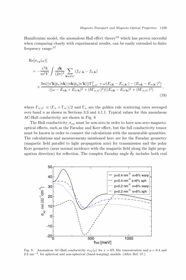
May 20, 2004 10:26 WSPC/140-IJMPB 02467
Magneto-Transport and Magneto-Optical Properties 1109
Hamiltonian model, the anomalous Hall effect theory52 which has proven succesful
when comparing closely with experimental results, can be easily extended to finite
frequency range:57
Re[σxy(ω)]
= − e2~
m2V
∫dk
(2π)3
∑
kn6=n′
(fn′,k − fn,k)
×Im[〈n′k|px|nk〉〈nk|py |n′k〉](Γ2
n,n′ + ω(Enk −En,k′) − (Enk −En,k′)2)
((ω −Enk +En′k)2 + (~Γn,n′)2)((Enk −En′k)2 + (~Γn,n′)2),
(19)
where Γn,n′ ≡ (Γn + Γn′)/2 and Γn are the golden rule scattering rates averaged
over band n as shown in Sections 3.3 and 4.1.1. Typical values for this anomlaous
AC-Hall conductivity are shown in Fig. 8
The Hall conductivity σxy must be non-zero in order to have non-zero magneto-
optical effects, such as the Faraday and Kerr effect, but the full conductivity tensor
must be known in order to connect the calculations with the measurable quantities.
The calculations and measurements mentioned here are for the Faraday geometry
(magnetic field parallel to light propagation axis) for transmission and the polar
Kerr geometry (near normal incidence with the magnetic field along the light prop-
agation direction) for reflection. The complex Faraday angle θF includes both real
0 500 1000h_
ω [meV]
-20
-10
0
10
20
30
40
50
σxy
(ω)
[Ω−
1cm
-1]
p=0.4 nm-3
x=6% warp
p=0.4 nm-3
x=6% sph
p=0.2 nm-3
x=6% warp
p=0.2 nm-3
x=6% sph
Fig. 8. Anomalous AC-Hall conductivity σxy(ω) for x = 6% Mn concentration and p = 0.4 and0.2 nm−3, for spherical and non-spherical (band-warping) models. (After Ref. 57.)
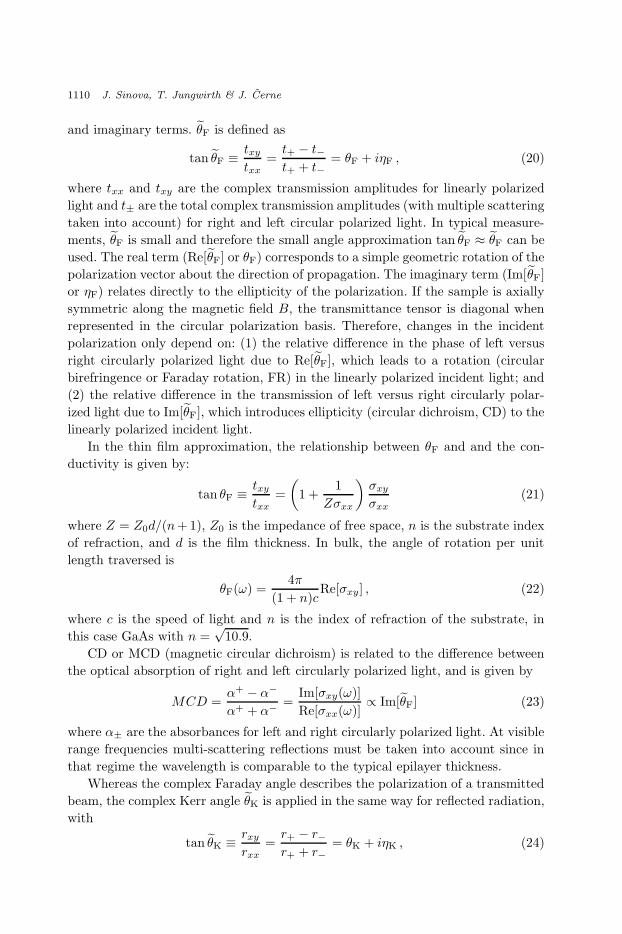
May 20, 2004 10:26 WSPC/140-IJMPB 02467
1110 J. Sinova, T. Jungwirth & J. Cerne
and imaginary terms. θF is defined as
tan θF ≡ txy
txx=t+ − t−t+ + t−
= θF + iηF , (20)
where txx and txy are the complex transmission amplitudes for linearly polarized
light and t± are the total complex transmission amplitudes (with multiple scattering
taken into account) for right and left circular polarized light. In typical measure-
ments, θF is small and therefore the small angle approximation tan θF ≈ θF can be
used. The real term (Re[θF] or θF) corresponds to a simple geometric rotation of the
polarization vector about the direction of propagation. The imaginary term (Im[θF]
or ηF) relates directly to the ellipticity of the polarization. If the sample is axially
symmetric along the magnetic field B, the transmittance tensor is diagonal when
represented in the circular polarization basis. Therefore, changes in the incident
polarization only depend on: (1) the relative difference in the phase of left versus
right circularly polarized light due to Re[θF], which leads to a rotation (circular
birefringence or Faraday rotation, FR) in the linearly polarized incident light; and
(2) the relative difference in the transmission of left versus right circularly polar-
ized light due to Im[θF], which introduces ellipticity (circular dichroism, CD) to the
linearly polarized incident light.
In the thin film approximation, the relationship between θF and and the con-
ductivity is given by:
tan θF ≡ txy
txx=
(1 +
1
Zσxx
)σxy
σxx(21)
where Z = Z0d/(n+ 1), Z0 is the impedance of free space, n is the substrate index
of refraction, and d is the film thickness. In bulk, the angle of rotation per unit
length traversed is
θF(ω) =4π
(1 + n)cRe[σxy] , (22)
where c is the speed of light and n is the index of refraction of the substrate, in
this case GaAs with n =√
10.9.
CD or MCD (magnetic circular dichroism) is related to the difference between
the optical absorption of right and left circularly polarized light, and is given by
MCD =α+ − α−
α+ + α−=
Im[σxy(ω)]
Re[σxx(ω)]∝ Im[θF] (23)
where α± are the absorbances for left and right circularly polarized light. At visible
range frequencies multi-scattering reflections must be taken into account since in
that regime the wavelength is comparable to the typical epilayer thickness.
Whereas the complex Faraday angle describes the polarization of a transmitted
beam, the complex Kerr angle θK is applied in the same way for reflected radiation,
with
tan θK ≡ rxy
rxx=r+ − r−r+ + r−
= θK + iηK , (24)

May 20, 2004 10:26 WSPC/140-IJMPB 02467
Magneto-Transport and Magneto-Optical Properties 1111
where rxx and rxy are the complex reflection amplitudes for linearly polarized light
and r± are the total complex reflection amplitudes (with multiple scattering taken
into account) for right and left circular polarized light.
Figure 9 shows the different magneto-optic effects predicted for a concentration
of x = 6% and p = 0.4 nm−3. The Faraday rotation in this case is larger than
the giant Faraday rotation observed in the paramagnetic (II,Mn)VI’s at optical
frequencies117 and should be readily observable in the highly metallic samples.
Though magneto-optical measurements on II–VI DMS materials have been ex-
tensive, see for example Ref. 121, measurements on III–V DMS have been more
limited, with almost no Faraday/Kerr measurements reported on these compounds
in the mid-infrared (MIR, 100–500 meV) range. The MIR range provides a critical
test of the predictions in Ref. 45. Transmission and reflection MIR magneto-optic
meaurements on Ga1−xMnxAs random alloy films in Figs. 10 and 11, respectively
have been recently measured in this MIR range and support the presence of such
strong magneto-optic signal in the MIR regime.122
0
0.05
0.1
0.15
0.2
MC
D
0
0.5
1
1.5
2
2.5
3
θF(ω
) [1
05 d
eg
/cm
]
0 250 500 750 1000-0.5
0
0.5
1
θK(ω
) [d
eg
]
0 250 500 750 1000h_
ω [meV]
-0.5
0
0.5
1
ηK(ω
) [d
eg
]
Fig. 9. Faraday and Kerr effects for x = 6% Mn concentration and p = 0.4 nm−3. (After Ref. 57.)

May 20, 2004 10:26 WSPC/140-IJMPB 02467
1112 J. Sinova, T. Jungwirth & J. Cerne
0.020
0.015
0.010
0.005
0.000
-0.005
-0.010
Re( θ
F)
(R
ad)
a)
0.020
0.015
0.010
0.005
0.000
Im( θ
F)
(Rad)
-0.6 -0.4 -0.2 0.0 0.2 0.4 0.6
Applied Magnetic Field (T)
b)
T = 7 Khν =120 meV
(a)
(b)
Im[θ
F] (
Rad
)R
e[ θ
F] (
Rad
)~
~
Fig. 10. Re[θF] (a) and Im[θF] in the MIR range (b) as a function of applied magnetic field forGaAs(6% Mn) random alloy epilayer at 7 K and probe radiation energy 118 meV, after Ref. 122.
Figure 10 plots the real (a) and imagnary (b) parts of the MIR [θF] probed at
a photon energy of 118 meV and a sample temperature of 7 K. The hysteresis is
weak and similar to out-of-plane DC magnetization measurements performed on
this sample (a 6% Ga1−xMnxAs random alloy film). Both the real and imaginary
parts of [θF] appear to be proportional to the film magnetization, as expected. The
Re[θF] signal at magnetization saturation calculated by Sinova et al.45 are on the
order of 0.04 rad for a film with a similar thickness and Mn concentration. However
such calculation are done in optimally annealed samples and further experimental
measurements in this more metallic regime will be helpful to establish the validity
of the model.
In Fig. 11, a two-step hysteresis loop is observed both the MIR (118 meV)
Re[θK] as well as the DC magnetization for a 1% Ga1−xMnxAs random alloy film.
This behavior is similar to that observed in MCD at a photon energy of 2.83 eV by
Ref. 108. The authors in Ref. 108 claim that such behavior cannot be attributed to
GaMn clusters, and therefore is a signature of the Ga1−xMnxAs alloy.

May 20, 2004 10:26 WSPC/140-IJMPB 02467
Magneto-Transport and Magneto-Optical Properties 1113
-3000 -2000 -1000 0 1000 2000 3000-80
-60
-40
-20
0
20
40
60
80
0011A at 7K
3000G -> -3000G
-3000G -> 3000G
Hysteresis of GaMnAs
M (
10-
6 em
u)
Field(Gauss)
Re
(θK)
(Rad
)
-0.008
-0.004
0.000
0.004
0.0087K
25K
35K
50K
95K
DC Magnetization
7 K
25 K35 K
50 K95 K
T = 7 K
hν = 118 meV
(a)
(b)
Applied Magnetic Field (Gauss)
Re[
θF]
(R
ad)
~
Fig. 11. Re[θK] and DC magnetization (courtesy of S. Wang) in the MIR (118 meV) regime forGaAs(1% Mn) random alloy epilayer. (After Ref. 122.)
The MIR magneto-optical measurement technique used in the above measure-
ments is described in detail in Ref. 123, and results using this technique on non-
magnetic systems are presented in Refs. 124 and 125. The results shown in Figs. 10
and 11 serve to demonstrate the experminetal feasibility of such studies, but further
work is required to interpret these results and to compare them with theoretical
predictions.
5. Summary
This review has focused on highlighting the rapid developments in material re-
search of metallic ferromagnetic (III,Mn)V semiconductors over the past few years.
Although the successes have been extensive in the understanding and development
of the bulk properties of the (Ga,Mn)As and (In,Mn)As systems within the metallic
regime, many challenges remain both in other (III,Mn)V based semiconductors and
lower dimensionalities such as digitally doped heterostructures. Both transport and

May 20, 2004 10:26 WSPC/140-IJMPB 02467
1114 J. Sinova, T. Jungwirth & J. Cerne
magneto-optical effects will remain a very fruitful ground to make progress in these
materials. At the time of writing, there is still a lot of work being done trying to
sort out the more complicated physics of (Ga,Mn)N and several reports of high Tc
measurements in the digitally doped materials. We keep watching in fascination
the rapid developments and challenges posed by new experiments which will un-
doubtedly generate interesting physics and new understandings of these fascinating
materials.
Acknowledgments
The many collaborators and colleagues with whom we have had the privilage to
work with and learn from are too numerous to name here and we are greatful for
their contribution to our knowledge of the subject. However, the authors would
like to acknowledge insightful discussions during the course of this review with
W. Atkinson, D. Basov, K. Burch, T. Dietl, J. Furdyna, H. Luo, J. Masek, A. H.
MacDonald, B. McCombe, C. Timm, and M. Weimer. This work was supported in
part by the Welch Foundation, DOE under grant DE-FG03-02ER45958, and the
Grant Agency of the Czech Republic under grant 202/02/0912.
References
1. H. Ohno, H. Munekata, T. Penney, S. von Molnar and L. L. Chang, Phys. Rev. Lett.
68, 2664 (1992).2. H. Ohno, Science 281, 951 (1998).3. S. Das. Sarma, E. H. Hwang and A. Kaminski (2003), cond-mat/0304219.4. C. Timm, J. Phys.: Condensed Matter 15, R1865 (2003).5. H. Ohno, J. Magn. Magn. Mater. 200, 110 (1999).6. T. Dietl, Semicond. Sci. Technol. 17, 377 (2002).7. F. Matsukura, H. Ohno and T. Dietl, Handbook of Magnetic Materials 14, 1 (2002).8. J. Konig, J. Schliemann, T. Jungwirth and A. MacDonald, in Electronic Structure
and Magnetism of Complex Materials, edited by D. Singh and D. Papaconstantopou-los (Springer-Verlag, Berlin, 2003).
9. T. Dietl, H. Ohno and F. Matsukura, Phys. Rev. B63, 195205 (2001).10. S. Sanvito, G. Theurich and N. Hill, J. of Superconductivity 15, 85 (2002).11. S. A. Wolf, D. D. Awschalom, R. A. Buhrman, J. M. Daughton, S. von Molnar, M.
L. Roukes, A. Y. Chtchelkanova and D. M. Treger, Science 294, 1488 (2001).12. T. Dietl, Acta Phys. Polon. A100, 139 (2001).13. J. F. Gregg, I. Petej, E. Jouguelet and C. Dennis, J. Phys. D: Appl. Phys. 35, R121
(2002).14. H. Ohno, F. Matsukura and Y. Ohno, JSAP International 5, 4 (2002).15. A. K. Bhattacharjee and C. B. a la Guillaume, Solid State Comm. 113, 17 (2000).16. M. Linnarsson, E. Janzen, B. Monemar, M. Kleverman and A. Thilderkvist, Phys.
Rev. B55, 6938 (1997).17. J. Schneider, U. Kaufmann, W. Wilkening, M. Baeumler and F. Kohl, Phys. Rev.
Lett. 59, 240 (1987).18. S. C. Erwin and A. Petukhov, Phys. Rev. Lett. 89, 227201 (2002).19. J. Masek and F. Maca (2002), cond-mat/0201131.

May 20, 2004 10:26 WSPC/140-IJMPB 02467
Magneto-Transport and Magneto-Optical Properties 1115
20. J. Szczytko, A. Twardowski, M. Palczewska, R. Jablonski, J. Furdyna and H.Munekata, Phys. Rev. B63, 085315 (2001).
21. J. Szczytko, A. Twardowski, K. Swiatek, M. Palczewska, K. A. M. Tanaka and T.Hayash, Phys. Rev. B60, 8304 (1999a).
22. J. Okabayashi, A. Kimura, T. Mizokawa A. Fujimori, T. Hayashi and M. Tanaka,Phys. Rev. B59, R2486 (1999).
23. J. Okabayashi, A. Kimura, O. Rader, T. Mizokawa, A. Fujimori, T. Hayashi and M.Tanaka, Phys. Rev. B64, 125304 (2001).
24. K. Edmonds, K. Wang, R. Campion, A. Neumann, N. Farley, B. Gallagher and C.Foxon, Appl. Phys. Lett. 81, 4991 (2002).
25. K. C. Ku, S. J. Potashnik, R. F. Wang, M. J. Seong, E. Johnston-Halperin, R. C.Meyers, S. H. Chun, A. Mascarenhas, A. C. Gossard, D. D. Awschalom, et al., Appl.
Phys. Lett. 82, 2302 (2003).26. R. Mathieu, B. S. Srensen, J. Sadowski, J. Kanski, P. Svedlindh and P. E. Lindelof
(2002), cond-mat/0208411.27. K. M. Yu, W. Walukiewicz, T. Wojtowicz, I. Kuryliszyn, X. Liu, Y. Sasaki and J.
K. Furdyna, Phys. Rev. B65, 201303 (2002).28. K. Edmonds, P. Boguslawski, K. Wang, R. Campion, N. Farley, B. Gallagher, C.
Foxon, M. Sawicki, T. Dietl, M. Nardelli, et al., Phys. Rev. Lett. 92, 037201 (2004).29. I. Kuryliszyn-Kudelska, T. Wojtowicz, X. Liu, J. K. Furdyna, W. Dobrowolski, J. Z.
Domagala, E. Lusakowska, M. Goiran, E. Haanappel and O. Portugall (2003).30. H. Ohno, D. Chiba, F. Matsukura, T. Omiya, E. Abe, T. Dietl, Y. Ohno and K.
Ohtani, Nature 408, 944 (2000).31. J. Szczytko, W. Mac, A. Twardowski, F. Matsukura and H. Ohno, Phys. Rev. B59,
12935 (1999).32. T. Omiya, F. Matsukura, T. Dietl, Y. Ohno, T. Sakon, M. Motokawa and H. Ohno,
Physica E7, 976 (2000).33. T. Dietl, Handbook of Semiconductors (1994).34. J. Masek, J. Kudrnovsky and F. Maca, Phys. Rev. B67, 153203 (2003).35. H. Akai, Phys. Rev. Lett. 81, 3002 (1998).36. J. Park, S. Kwon and B. Min, Physica B281/282, 703 (2000).37. J. Masek and F. Maca, Acta Phys. Polon. A102, 667 (2002).38. J. Blinowski and P. Kacman, Phys. Rev. B67, 121204 (2003).39. T. Jungwirth, J. Masek, J. Sinova and A. MacDonald, Phys. Rev. B68, 161202(R)
(2003).40. R. Campion, K. Edmonds, L. Zhao, K. Wang, C. Foxon, B. Gallagher and C. Stad-
don, J. Cryst. Growth 251, 311 (2003).41. R. N. Bhatt, M. Berciu, M. P. Kennett and X. Wan, J. of Superconductivity 15, 71
(2002).42. M. Abolfath, T. Jungwirth, J. Brum and A. MacDonald, Phys. Rev. B63, 054418
(2001).43. I. Vurgaftman, J. Meyer and L. Ram-Mohan, J. Appl. Phys 89, 5815 (2001).44. T. Jungwirth, M. Abolfath, J. Sinova, J. Kucera and A. MacDonald, Appl. Phys.
Lett. 81, 4029 (2002).45. J. Sinova, T. Jungwirth, S.-R. E. Yang, J. Kucera and A. MacDonald, Phys. Rev.
B66, 041202 (2002).46. S.-R. E. Yang, J. Sinova, T. Jungwirth, Y. Shim and A. MacDonald, Phys. Rev.
B69, 085209 (2003).47. J. Schliemann, Phys. Rev. B67, 045202 (2002).

May 20, 2004 10:26 WSPC/140-IJMPB 02467
1116 J. Sinova, T. Jungwirth & J. Cerne
48. J. Schliemann and A. MacDonald, Phys. Rev. Lett. 88, 137201 (2002).49. B. Lee, T. Jungwirth and A. MacDonald, Semicond. Sci. Technol. 17, 393 (2002).50. T. Dietl, H. Ohno, F. Matsukura, J. Cibert and D. Ferrand, Science 287, 1019
(2000).51. T. Jungwirth, J. Konig, J. Sinova, J. Kucera and A. MacDonald, Phys. Rev. B66,
012402 (2002).52. T. Jungwirth, J. Sinova, K. Wang, K. W. Edmonds, R. Campion, B. Gallagher, C.
Foxon, Q. Niu and A. MacDonald, Appl. Phys. Lett. 83, 320 (2003).53. T. Jungwirth, Q. Niu and A. MacDonald, Phys. Rev. Lett. 88, 207208 (2002).54. J. Konig, T. Jungwirth and A. MacDonald, Phys. Rev. B64, 184423 (2001).55. T. Dietl, J. Konig and A. H. MacDonald, Phys. Rev. B64, 241201 (2001).56. J. Sinova, T. Jungwirth, Y. S. X. Liu, J. Furdyna, W. A. Atkinson and A. MacDonald
(2003).57. J. Sinova, T. Jungwirth, J. Kucera and A. MacDonald, Phys. Rev. B67, 235203
(2003).58. A. Chattopadhyay, S. D. Sarma and A. J. Millis, Phys. Rev. Lett. 87, 227202 (2001).59. F. Matsukura, H. Ohno, A. Shen and Y. Sugawara, Phys. Rev. B57, R2037 (1998).60. S. J. Potashnik, K. C. Ku, S. H. Chun, R. F. Wang, M. B. Stone, N. Samarth and
P. Schiffer (2002), cond-mat/0212260.61. A. V. Esch, L. V. Bockstal, J. D. Boeck, G. Verbanck, A. S. van Steenbergen, P.
J. Wellmann, B. Grietens, R. B. F. Herlach and G. Borghs, Phys. Rev. B56, 13103(1997).
62. T. Hayashi, M. Tanaka, K. Seto, T. Nishinaga and K. Ando, Appl. Phys. Lett. 71,1825 (1997).
63. M. Lopez-Sancho and L. Brey, Phys. Rev. B68, 113201 (2003).64. S. J. Potashnik, K. C. Ku, R. Mahendiran, S. H. Chun, R. F. Wang, N. Samarth
and P. Schiffer, Phys. Rev. B66, 012408 (2002).65. D. V. Baxter, D. Ruzmetov, J. Scherschligt, Y. Sasaki, X. Liu, J. K. Furdyna and
C. H. Mielke, Phys. Rev. B65, 212407 (2002).66. K. W. Edmonds, R. P. Campion, K.-Y. Wang, A. C. Neumann, B. L. Gallagher, C.
T. Foxon and P. C. Main, J. Appl. Phys. 93, 6787 (2002).67. K. Wang, K. Edmonds, R. Campion, L. Zhao, A. Neumann, C. Foxon, B. Gallagher
and P. Main (2002), cond-mat/0211697.68. H. Tang, R. Kawakami, D. Awschalom and M. Roukes, Phys. Rev. Lett. 90, 107201
(2003).69. Sometimes it is called extraordinary or spin Hall effect, although these names are now
in disuse and the later one is now used in a different context within paramagneticmaterials.
70. L. Chien and C. R. Westgate, The Hall Effect and Its Applications (Plenum, NewYork, 1980).
71. R. Karplus and J. Luttinger, Phys. Rev. 95, 1154 (1954).72. J. Smit, Physica 21, 877 (1955).73. W. Kohn and J. Luttinger, Phys. Rev. 108, 590 (1957).74. J. Luttinger, Phys. Rev. 112, 739 (1958).75. E. Adams and E. Blount, J. Phys. Chem. Solids 10, 286 (1959).76. L. Berger, Phys. Rev. B2, 4559 (1970).77. S. Lyo and T. Holstein, Phys. Rev. Lett. 29, 423 (1972).78. P. Leroux-Hugon and A. Ghazali, J. Phys. C5, 1072 (1972).79. P. Nozieres and C. Lewiner, Le Journal de Physique 34, 901 (1973).80. R. Fivaz, Phys. Rev. 183, 586 (1969).

May 20, 2004 10:26 WSPC/140-IJMPB 02467
Magneto-Transport and Magneto-Optical Properties 1117
81. J. Chazalviel, Phys. Rev. B11, 3918 (1975).82. T. Dietl, F. Matsukura, H. Ohno, J. Cibert and D. Ferrand (2003), cond-
mat/0306484.83. J. Smit, Phys. Rev. B8, 2349 (1973).84. L. Berger, Phys. Rev. B8, 2351 (1973).85. J. Smit, Phys. Rev. B17, 1450 (1978).86. L. Berger, Phys. Rev. B17, 1453 (1978).87. A. Crepieux and P. Bruno, Phys. Rev. B64, 014416 (2001).88. A. Crepieux and P. Bruno, Phys. Rev. B64, 094434 (2001).89. V. K. Dugaev, A. Crepieux and P. Bruno, Phys. Rev. B64, 104411 (2001).90. M. Onoda and N. Nagaosa, J. Phys. Soc. Jap. 71, 19 (2001).91. Z. Fang, N. Nagaosa, K. S. Takahashi, A. Asamitsu, R. Mathieu, T. Ogasawara, H.
Yamada, M. Kawasako, Y. Tokura and K. Terakura, Science 302, 92 (2003).92. Y. Taguchi, Y. Oohara, H. Yoshizawa, N. Nagaosa and Y. Tokura, Science 291, 2573
(2001).93. R. Shindou and N. Nagaosa, Phys. Rev. Lett. 87, 116801 (2001).94. J. Ye, Y. B. Kim, A. J. Millis, B. I. Shraiman, P. Majumdar and Z. Tesanovic, Phys.
Rev. Lett. 83, 3737 (1999).95. Y. Yao, L. Kleinman, A. H. MacDonald, J. Sinova, T. Jungwirth, D. S. Wang, E.
Wang and Q. Niu, Phys. Rev. Lett. 86, 037204 (2004).96. K. W. Edmonds, K. Y. Wang, R. P. Campion, A. C. Neumann, C. T. Foxon, B. L.
Gallagher and P. C. Main, Appl. Phys. Lett 81, 3010 (2002).97. A. Burkov and L. Balents, Phys. Rev. Lett. 91, 057202 (2003).98. C. Timm, F. von Oppen and F. Holfing (2003), con-mat/0309547.99. P. Bruno, V. K. Dugaev and M. Taillefumier (2003), cont-mat/0310522.
100. E. J. Singley, R. Kawakami, D. D. Awschalom and D. N. Basov, Phys. Rev. Lett.
89, 097203 (2002).101. E. J. Singley, K. S. Burch, R. Kawakami, J. Stephens, D. D. Awschalom and D. N.
Basov, Phys. Rev. B68, 165204 (2003).102. R. A. Chapman and W. G. Hutchinson, Phys. Rev. Lett. 18, 443 (1967).103. K. Hirakawa, S. Katsumoto, T. Hayashi, Y. Hashimoto and Y. Iye, Phys. Rev. B65,
193312 (2002).104. K. Hirakawa, A. Oiwa and H. Munekata, Physica E10, 215 (2001).105. Y. Nagai, T. Kunimoto, K. Nagasaka, H. Nojiri, M. Motokawa, G. Matsukura, T.
Dietl and H. Ohno, Jpn. J. Appl. Phys. 40, 6231 (2001).106. J. Szczytko, A. Stachow, W. Mac, A. Twardowski, P. Belca and J. Tworzydlo, Acta
Physica Polonica 90, 951 (1996).107. B. Beschoten, P. Crowell, I. Malajovich and D. Awschalom, Phys. Rev. Lett. 83,
3073 (1999).108. K. Ando, T. Hayashi, M. Tanaka and A. Twardowski, J. Appl. Phys. 83, 6548 (1998).109. M. J. Seong, S. H. Chun, H. M. Cheong, N. Samarth and A. Mascarenhas, Phys.
Rev. B66, 033202 (2002).110. W. Limmer, M. Glunk, S. Mascheck, A. Koeder, W. Scoch, K. Thonke, R. Sauer
and A. Waag, Phys. Rev. B66, 205209 (2002).111. V. F. Sapega, T. Ruf and M. Cardona, Phys. Stat. Sol. B226, 339 (2001).112. J. Okabayashi, T. Mizokawa, D. D. Sarma, A. Fujimori, T. Slupinski, A. Oiwa and
H. Munekata, Phys. Rev. B65, 161203 (2002).113. H. Asklund, L. Ilver and J. S. J. Kanski, Phys. Rev. B66, 115319 (2002).114. G. A. Khodaparast, J. Kono, Y. H. Matsuda, S. Ikeda, N. Miura, T. Slupinski, A.
Oiwa, H. Munekata, Y. Sun and F. V. Kyrychenko, et al. (2003), cond-mat/0307087.

May 20, 2004 10:26 WSPC/140-IJMPB 02467
1118 J. Sinova, T. Jungwirth & J. Cerne
115. G. D. Sanders, Y. Sun, F. V. Kyrychenko, C. J. Stanton, G. A. Kodaparast, M. A.Zudov, J. Kono, N. M. Y. H. Matsuda and H. Munekata Phys. Rev. B68, 165205(2003).
116. Y. Mitsumori, A. Oiwa, T. Slupinski, H. Maruki, Y. Kashimura, F. Minami and H.Munekata (2003), cond-mat/0307268.
117. S. Sugano and N. Kojima, Magneto-Optics (Springer-Verlag, New York, 2000).118. E. H. Hwang, A. J. Millis and S. D. Sarma, Phys. Rev. B65, 233206 (2002).119. G. Alvarez and E. Dagotto, Phys. Rev. B68, 045202 (2003).120. M. Takahashi (2003), cond-mat/0306588.121. A. Ramdas and H. Alawadhi, Current Science 75, 1216 (1998).122. J. Cerne et al., to be published.123. J. Cerne, D. Schmadel, L. Rigal and H. Drew, Rev. Sci. Instr. 74, 4755 (2003).124. J. Cerne, M. Grayson, D. Schmadel, G. Jenkins, H. D. Drew, R. Hughes, J. Preston
and P. Kung, Phys. Rev. Lett. 84, 3418 (2000).125. J. Cerne, D. Schmadel, M. Grayson, G. Jenkins, J. R. Simpson and H. D. Drew,
Phys. Rev. B61, 8133 (2000).


![Magneto-optical trapping forces for atoms and …Magneto-optical trapping forces for atoms and molecules 2 1. Introduction The magneto-optical trap (MOT) [1] is a crucial tool for](https://img.dokumen.tips/doc/110x75/5e8cc964236bf92dee25ab86/magneto-optical-trapping-forces-for-atoms-and-magneto-optical-trapping-forces-for.jpg)