Embed Size (px)
Citation preview
ARTICLE IN PRESS
Neurocomputing 73 (2010) 1222–1234
Contents lists available at ScienceDirect
Neurocomputing
0925-23
doi:10.1
� Corr
E-m
journal homepage: www.elsevier.com/locate/neucom
Łukasiewicz fuzzy logic networks and their ultra low power hardwareimplementation
Rafa" D"ugosz a,�, Witold Pedrycz b,c
a Swiss Federal Institute of Technology in Lausanne, Institute of Microtechnology, Rue A.-L. Breguet 2, CH-2000, Neuchatel, Switzerlandb University of Alberta, Department of Electrical and Computer Engineering ECERF Building, Edmonton, Canada T6G 2V4c Systems Research Institute, Polish Academy of Sciences, Warsaw, Poland
a r t i c l e i n f o
Available online 18 January 2010
Keywords:
Neural networks
Logic neurons
Fuzzy sets
CMOS analog devices
Ultra low power electronics
12/$ - see front matter & 2010 Elsevier B.V. A
016/j.neucom.2009.11.027
esponding author.
ail address: [email protected] (R. D"ugosz)
a b s t r a c t
In this paper, we propose a new category of current-mode Łukasiewicz OR and AND logic neurons and
ensuing logic networks along with their ultra-low power realization. The introduced circuits can
operate in a wide range of the input signals varying in-between 10 nA and 10mA. For low current values
the operating point of transistors is set in the under threshold region. In this region, the mismatch
between transistors exhibits a far stronger impact on the current mirror precision than the one
observed in case of the strong inversion region. The proposed design alleviates this problem by reducing
the number of current mirrors between the input and the output of the neuron and of the overall
network to only one. Łukasiewicz operators require only summation and subtraction operations, which
make them suitable for realization in analog current-mode technique. In this case even large number of
input signals can be summed in a simple junction in a single step. This is the reason of choosing
Łukasiewicz operations in the proposed circuit. Using other t-norm and t-conorm operations with
multiplication and division operations would make the realization of the circuit very difficult and
inefficient.
& 2010 Elsevier B.V. All rights reserved.
1. Introduction
Neurocomputing has emerged as a synonym of adaptiveprocessing and significant learning capabilities. Fuzzy sets,treated as one of the branches of Granular Computing, are aboutprocessing information granules which are commonly encoun-tered in human perception and information processing. Thelimitations of these two technologies (viz. fuzzy sets andneurocomputing) when being considered individually, are sig-nificantly eliminated by forming hybrid architectures known asneurofuzzy systems. In this synergistic environment we take fulladvantage of the learning capabilities of neural networks whilebenefiting from transparency of processing coming hand in handwith fuzzy sets. Fuzzy neural networks as introduced e.g., in[9,11] are examples of such hybrid architectures of neurocomput-ing.
In a nutshell, we can view these networks as an essentialgeneralization of two-valued digital circuits which are nowaugmented by significant learning capabilities and flexibility todeal with continuous inputs viewed as truth values encounteredin fuzzy logic and multivalued logic. As such, we can refer to aplethora of areas in which the use of neurofuzzy structures of this
ll rights reserved.
.
nature can be considered including: (a) pattern recognition, (b)rule-based systems (and approximate reasoning, in general), (c)logic-oriented models, (d) fuzzy and neural control, to name a fewgeneral categories.
Surprisingly enough, there has been a very limited research inhardware implementation and ensuing design practice of archi-tectures of neurofuzzy systems. We can refer here to a fewpublications dealing with this subject matter, cf. [1,4,7,8]. In somesense, this is quite impeding considering a wealth of newpotential applications of intelligent systems associated withmobile and pervasive computing as being vigorously promotedin the realm of ambient intelligence (AmI). One of the funda-mental quests comes with regard to power consumption whoseminimal level becomes highly beneficial to mobile devices. Thissomewhat implies intensive studies along the line of analogelectronics.
The objective of this study is to introduce one of the variants ofneurocomputing coming in the form of fuzzy neural networkswhose neurons are realized by means of Łukasiewicz operators(and and or operators). The Łukasiewicz operators are a soundalternative which offers enough flexibility with regard to under-lying logic processing which comes with appealing featuressupporting the hardware realization of these neurons.
The study is organized as follows. In Section 2, we start, with abrief introduction to Łukasiewicz logic operators. The motivationof choosing the Łukasiewicz operators in the context of realization

ARTICLE IN PRESS
R. D!ugosz, W. Pedrycz / Neurocomputing 73 (2010) 1222–1234 1223
of logic processors (LP) has been highlighted in Section 3. InSection 4, we propose Łukasiewicz networks when using the‘‘classic’’ approach to the realization of the fuzzy operationsproposed by Yamakawa in [15]. The discussed limitations of thisclassic approach led us to the proposal of the new approach to theimplementation of such networks (Section 5), along with simula-tion results reported at the transistor level. The conclusions areoffered in Section 6. Throughout the paper we will adhere to thestandard notation used in fuzzy sets.
2. Łukasiewicz logic operations
Łukasiewicz logic connectives arise as one of the possiblerealizations of logic operators applied to fuzzy sets [6]. Those areinteresting examples of a broad category of logic connectivesknown as t-norms and t-conorms. Interestingly, those operationswere originally introduced by Łukasiewicz in his original studieson three-valued and multiple-valued logic. More formally, theŁukasiewicz and operator is described as follows:
atb¼maxð0; aþb�1Þ ð1Þ
while the or operator is governed by the following expression
asb¼minð1; aþbÞ ð2Þ
where the (logic) truth values a and b assume values in the unitinterval.
These logic connectives can be arranged together in theconstructs of logic neurons that are viewed as generic processingunits encountered in logic neurocomputing. Logic neurons [10]offer functionality which embraces advantages of neural networksas far as learning is concerned and fuzzy logic which becomesadvantageous with respect to the associated interpretationabilities. The logic neurons come with well-defined semantics,which is drawn from the nature of the underlying logic processinginherent to fuzzy computing. We encounter two fundamentalcategories of fuzzy neurons.
OR neuron: this neuron realizes an and logic aggregation ofinputs x=[x1 x2yxn]T with the corresponding connections(weights) w=[w1 w2ywn]T and then summarizes the partialresults in an or-wise manner (hence the name of the neuron). Theconcise notation underlines this flow of computing, y=OR(x; w)while the realization of the logic operations gives rise to theexpression (commonly referred to as an s–t combination or s–taggregation)
yOR ¼ Sn
i ¼ 1ðxitwiÞ ð3Þ
Here ‘‘t’’ denotes a certain t-norm whereas ‘‘s’’ refers to some t-conorm (s-norm). Bearing in mind the interpretation of the logicconnectives, the OR neuron realizes the following logic expressionbeing viewed as an underlying logic description of the processingof the inputs
yOR ¼ ðx1 and w1Þ or ðx2 and w2Þ or . . . orðxn and wnÞ ð4Þ
Apparently here the inputs are logically ‘‘weighted’’ by the valuesof the connections (wi) before producing the final result. In otherwords we can treat ‘‘y’’ as a truth value of the above statementwhere the truth values of the inputs are affected by thecorresponding weights. Noticeably, lower values of wi discountthe impact of the corresponding inputs; higher values of theconnections (especially those being positioned close to 1) do notaffect the original truth values of the inputs. In limit, if allconnections wi, i=1, 2,y,n are set to 1 then the neuron produces aplain or-combination of its inputs:
yOR ¼ x1 or x2 or . . . or xn ð5Þ
The values of the connections set to zero eliminate thecorresponding inputs. Computationally, the OR neuron exhibitsnonlinear characteristics (that is inherently implied by the use ofthe t- and t-conorms).
AND neuron: the neurons in the category, denoted byy=AND(x; w) with x and w being defined as in case of the ORneuron, are governed by the expression
yAND ¼ Tn
i ¼ 1ðxiswiÞ ð6Þ
In comparison with the previous category of the neurons, here theor and and connectives are used in a reversed order:
yAND ¼ ðx1 or w1Þ and ðx2 or w2Þ and . . . and ðxn or wnÞ ð7Þ
first the inputs are combined with the use of the t-conorm and thepartial results produced in this way are aggregated and-wise.Higher values of the connections reduce impact of the corre-sponding inputs. In limit wi=1 eliminates the relevance of xi. Withall wi set to 0, the output of the AND neuron is just an and
aggregation of the inputs
yAND ¼ x1 and x2 and . . . and xn ð8Þ
2.1. Additional functional features of logic neurons
While the above constructs could be viewed as generic logicneurons, there are two interesting and useful augmentations ofthe neurons which bring them even closer to the topologies of‘‘standard’’ neurons existing in the realm of neurocomputing.
Incorporation of bias term: In analogy to the generic neuron aspresented above, we could also consider a bias term, denoted byw0 A[0, 1] which enters the processing formula of the fuzzyneuron in the following way
for the OR neuron
yOR ¼ Sn
i ¼ 1ðxitwiÞsw0 ð9Þ
for the AND neuron
yAND ¼ Tn
i ¼ 1ðxiswiÞtw0 ð10Þ
We can offer some useful interpretation of the bias by treating itas some nonzero initial truth value associated with the logicexpression of the neuron. For the OR neuron it means that theoutput does not reach values lower than the assumed threshold.For the AND neuron equipped with some bias, we conclude thatits output cannot exceed the value assumed by the bias. Thequestion whether the bias is essential in the construct of the logicneurons cannot be fully answered in advance. Instead, we mayinclude it into the structure of the neuron and carry out learning.Once its value has been obtained, its relevance could beestablished considering the specific value it has been producedduring the learning. It may well be that the optimized value of thebias is close to zero for the OR neuron or close to one in the case ofthe AND neuron which indicates that it could be eliminatedwithout exhibiting any substantial impact on the performance ofthe neuron.
Inhibitory functionality of logic neurons: Owing to the mono-tonicity of the t-norms and t-conorms, the computing realized bythe neurons exhibits an excitatory character. This means thathigher values of the inputs (xi) contribute to the increase in thevalues of the output of the neuron. The inhibitory nature ofcomputing realized by ‘‘standard’’ neurons by using negativevalues of the connections or the inputs is not available here as thetruth values (membership grades) in fuzzy sets are confined to theunit interval. The inhibitory nature of processing can beaccomplished by considering the complement of the original

ARTICLE IN PRESS
R. D!ugosz, W. Pedrycz / Neurocomputing 73 (2010) 1222–12341224
input, xi ¼ 1�xi. Hence when the values of xi increase, theassociated values of the complement decrease and subsequentlyin this configuration we could effectively treat such an input ashaving an inhibitory nature.
3. Logic processor in the processing of fuzzy logic functions: acanonical realization
The typical logic network that is at the center of logicprocessing originates from the two-valued logic and comes inthe form of the well-known Shannon theorem of decompositionof Boolean functions. Let us recall that any Boolean function{0,1}n-{0,1} can be represented as a logic sum of its correspond-ing minterms or a logic product of maxterms. By a minterm of ‘‘n’’logic variables x1, x2,y, xn we mean a logic product involving allthese variables either in direct or complemented form. Having ‘‘n’’variables we end up with 2n minterms starting from the oneinvolving all complemented variables and ending up at the logicproduct with all direct variables. Likewise by a maxterm we meana logic sum of all variables or their complements. Now in virtue ofthe decomposition theorem, we note that the first representationscheme involves a two-layer network where the first layerconsists of AND gates whose outputs are combined in a singleOR gate. The converse topology occurs for the second decom-position mode: there is a single layer of OR gates followed by asingle AND gate aggregating or-wise all partial results.
The proposed network (referred here as a logic processor–LP)generalizes this concept as shown in Fig. 1. The AND-OR mode ofthe logic processor comes with the two types of aggregativeneurons being swapped between the layers. Here the first(hidden) layer is composed of the AND neuron and is followedby the output realized by means of the OR neuron.
The logic neurons generalize digital gates. The design of thenetwork (viz. any fuzzy function) is realized through learning. Ifwe confine ourselves to {0,1} values, the network’s learningbecomes an alternative to a standard digital design, especially aminimization of logic functions. The logic processor translatesinto a compound logic statement (we skip the connections of theneurons to emphasize the underlying logic content of thestatement itself):
ifðinput1 and . . . and inputjÞ or ðinputd and . . . and inputf Þ then output
ð11Þ
The LP’s topology (and its underlying interpretation) is standard.Two LPs can vary in terms of the number of AND neurons, theirconnections but the format of the resulting logic expression isquite uniform (as a sum of generalized minterms).
It is worth noting that there is an infinite family of t- and s-normswhich can be used in the realization of logic neurons. One has to becognizant that some of these operators are more suitable forhardware realization. Let us consider some common cases in detail:
Fig. 1. A topology of the logic processor in its AND–OR mode.
(a) The minimum operator and maximum operator are easy torealize yet their input–output characteristics are limited. Inparticular, we observe a so-called lack of interactivity betweenthe arguments. The operator exhibits an ‘‘extreme’’ behavior inthe sense it picks up the most extreme argument (viz. the onewith the minimal or maximal value). The result does not dependon the location (numeric values) of other arguments.
(b) the product operator is free from this shortcomings yet themultiplication operation is much more difficult to be realized inhardware. This problem is especially visible in case of manyinputs like those shown in Eq. (7). In this case the multiplicationwould have to be repeated n times, while known electronicmultipliers required to realize this task are either of low precisionor become overly complex.
Given these computational and implementation requirements,we can arrive at conclusion that the Łukasiewicz connectives forman interesting alternative as being computationally flexibleenough while still maintaining some features appealing fromthe implementation perspective. Łukasiewicz operators requireonly summation and subtraction operations, which makes themsuitable for realization in analog current-mode technique. In thiscase even a large number of the input signals can be summed in asimple junction in a single processing step that simplifies theoverall circuit.
Typical calculation scheme applied to Eqs. (4) and (7) is ofiterative nature. This means that first we calculate either the or orthe and operation using only two network inputs. Then the resultof this operation is used as the input to the same operation at thesecond step together with the third network input. For n networkinputs we need n or or and operations realized in a cascademanner. By using the Łukasiewicz operations, we reduce thiscalculation scheme to a single step only, since summation of allinput signals represented by currents is realized in a junction inparallel. This significantly speeds up the calculations realized bysuch network and simplifies an overall structure of the circuit.
For illustrative purposes, Figs. 2 and 3 present input–outputcharacteristics of the AND and OR neurons being implemented bymeans of the Łukasiewicz connectives. Note that the piecewiselinear nature of the characteristics is highly visible while thedetailed geometry of the neurons is implied by the values of theconnections. Likewise we note a piecewise (and hence nonlinear)nature of the overall network.
4. Implementation of the OR and the AND neurons usingclassic CMOS fuzzy operators
Basic fuzzy logic operators together with their classic CMOShardware implementation have been described in [15]. To realizethese operators, the current-mode technique is the most suitableas it is suitable for an easy realization of summation andsubtraction operations. The literature study shows that thistechnique is the most commonly used for this purpose [1,4,7,8].The logic or and the and operators are also referred to as thebounded sum and the bounded product, respectively [15]. Usingthe approach presented in [15] we first propose the logicprocessor shown in Fig. 4. This figure presents a simplifieddiagram of the Łukasiewicz network that consists of two layers ofneurons. In this case, the network comes in the AND-ORconfiguration, as shown in Fig. 1, although the dualconfiguration, that is OR–AND, arises as another alternativetopology.
As mentioned above, the current-mode technique offers a veryeffective platform for the implementation of the logic operators,however it is a source of limited accuracy of these circuits. One ofthe main problems encountered in this realization is a mismatch

ARTICLE IN PRESS
Fig. 2. Input–output characteristics of the AND neuron with 2 inputs (x1 and x2) and 2 corresponding weights; the cases from the left to the right are given for the following
weights (w1,w2): [(0,0); (0.2,0.2); (0.5, 0.5); (1,1)].
Fig. 3. Input–output characteristics of the OR neuron with 2 inputs (x1 and x2) and 2 corresponding weights; the cases from the left to the right are given for the following
weights (w1,w2): [(0,0); (0.2,0.2); (0.5, 0.5); (1,1)].
and1
or function
1n-
max
(0,1
-
1
11
AND neuron
1 1
max
(0,
-1)
max(0, -1)
OR neuron
1
and rodna
current mirrorPMOS
NMOS current mirror
mor1
min(1, mor2 ) min(1, mor n) mandi
1wOR1yAND
yOR
man
d1
min
(1,
)m
or1
)m
or1
m
Fig. 4. Implementation of an example AND–OR Łukasiewicz network using
Yamakawa’s approach [14]. Terms mor i=xi+wi and mand i=yAND i+wOR i are used
for simplifying the variables description.
R. D!ugosz, W. Pedrycz / Neurocomputing 73 (2010) 1222–1234 1225
between transistors present in the current mirrors [12]. Usually,the threshold voltage mismatch, DVth, is assumed to be the mainreason causing mismatch between the transistors working in acurrent mirror and therefore we limit our study to this parameteronly. In practice several other mismatch components will furtherdistort the signal. Assuming that both transistors have equal sizesthen in the under threshold region the current mirror’s gain thatresults from DVth can be calculated as follows [2]:
I2
I1¼ e�DVth=nVT ð12Þ
while in the strong inversion region is expressed as
I2
I1¼ðVGS�VTH�DVTHÞ
2
ðVGS�VTHÞ2
ð13Þ
where VT is the thermal voltage (about 26 mV in the roomtemperature of 300 K). The influence of the transistor dimensionson the mismatch effect for different technologies has beenreported and studied in many papers. The example diagramillustrating this phenomenon is shown in Fig. 5. For instance, inthe CMOS 0.18mm process, the standard deviation of the Vth
mismatch varies in-between 0.7 and 2.9 [mV] given that thetransistor gate’s area (W � L) varies in the range between 75 and3mm2 [3].
In the under threshold region of operation, this effectintroduces to the current mirror a gain error of 3% for largetransistors; however this error could be as high as 11% for smalltransistors with an example gate area of 3mm2. This effect isillustrated in Fig. 6; refer to the upper curve. In the stronginversion region—the lower curve in Fig. 6—the influence of themismatch on the gain is about 6–8 times smaller, but it is stillimportant in case of circuits with large number of intermediatecurrent mirrors like, for example, in the circuit shown in Fig. 4. Inthis case the number of current mirrors between the inputs andthe output equals to 6. For large transistors with sizes of e.g. W/L=15/3mm working in the strong inversion regime, the error of10–15% is realistic, while in the under threshold region this errorcould be even as high as 40–60%. This makes the precision of the

ARTICLE IN PRESS
0
1
2
3
4
5
6
7
0 0.2 0.4 0.6 0.8 11/sqrt (WL) [1/µm]
σ(ΔV
T) [m
V]
10/7.2
1.9/2.7
4/4
1.4/1.9
0.35/5.3
0.25/7.2 &0.55/3.3
4.2/0.45
7.1/0.25
10/0.18
1/1
Fig. 5. Influence of transistor sizes on threshold voltage mismatch in CMOS 0.18mm technology [2].
0
2
4
6
8
10
12
4321the case (W/L)
e [%
]
strong inversion region
under threshold region
W/L=1 / 3 µm
3 / 3 µm9 / 3 µm 15 / 3 µm
Fig. 6. Influence of transistor sizes on the gain error of a single current mirror in under threshold (upper curve) and strong inversion (bottom curve) regions, in CMOS
0.18mm technology, for currents with an example constant value of 10mA and the supply voltage VDD of 1.8 V.
R. D!ugosz, W. Pedrycz / Neurocomputing 73 (2010) 1222–12341226
network based on the classic approach shown in Fig. 4insufficient.
Fig. 6 illustrates another interesting phenomenon. The givenvalues of the gain error are, for example, constant currents of10mA. In the strong inversion region this error depends not onlyon transistor sizes but also on the value of the gate to sourcevoltage, VGS, as shown in Eq. (13). Theoretically by increasing thetransistor sizes we limit this error due to improved matching, butby keeping the currents at the same level we decrease the value ofthe VGS voltage that increases the value of this error. As a result,both effects compensate one another thus resulting in almostconstant value of this error seen in the bottom curve, with aminimum value for the aspect ratio (W/L) of 9/3mm in this case.To make some further performance improvement in the stronginversion region possible it is necessary to increase the values ofthe currents, which will increase the value of the VGS voltage.Unfortunately increasing the currents increases the powerdissipation, so there is a trade-off between this parameter andthe circuit precision.
To overcome the serious drawback described above, wepropose the realization of new neurons described in the nextsection. The circuits built in this manner take advantage of thecurrent mode, but the number of intermediate mirrors has beensignificantly reduced. In this case, signal paths between the inputsand the output of the circuit are controlled by simple current-mode comparators, realized using binary CMOS inverters andswitches. This approach allows for significantly improved perfor-
mance, since now the error of the overall network is limited to theerror of a single current mirror only. Considering the resultspresented in Fig. 6, in the proposed network the aspect ratios (W/L) of 6/3 and 2/3mm have been selected for the PMOS and theNMOS transistors respectively.
5. The proposed realization of the Łukasiewicz OR and ANDlogic neurons
5.1. OR neuron
The output of the multi-input OR neuron when implementedin software is commonly calculated in an iterative fashion byusing the following expression:
yOR ¼ ðððyand 1 or yand 2Þ or yand 3Þ or . . . or yand nÞ ð14Þ
where the outputs of the particular and functions are determinedas follows:
yand i ¼maxð0; xiþwi�1Þ ð15Þ
Analyzing this expression from the left, the first or function in (14)returns either yand 1+yand 2 or 1, depending on which of thesecomponents assumes lower value. If yand 1+yand 2 is smaller thenthe next or function in the chain compares yand 1+yand 2+yand 3
with 1, returning the smaller of these terms. It can be shown thatif at least one of these or functions returns 1 then all other or

ARTICLE IN PRESS
R. D!ugosz, W. Pedrycz / Neurocomputing 73 (2010) 1222–1234 1227
functions also return 1. Since in hardware implementations manyoperations can be performed in parallel, therefore in this case it ismuch more convenient to use another scheme, which can beexpressed as follows:
yOR ¼minð1;Xn
i ¼ 1
yand iÞ ð16Þ
(15) is very inconvenient to be implemented in the current-modetechnique. The term after the coma can be either negative orpositive when being compared with 0. Negative currents requiremuch more complex circuits and therefore this expression mustbe transformed to avoid such a situation. The same result weobtain using the following formula:
yand i ¼maxð1; xiþwiÞ�1 ð17Þ
In this case we always compare only positive signals. Now themax function always returns the signal that is greater or equal to1 and therefore subtraction of 1 in this equation never makes theoutput signal to be negative. Introducing new binary variables sai
and sOR, defined as
sai ¼1 for xiþwi41
0 otherwiseand sOR ¼
1 forXn
i ¼ 1
yand io1
0 otherwise
8><>:
8><>: ð18Þ
(17) can be rewritten as
yand i ¼ saiðxiþwi�1Þ ð19Þ
while (14) reads as follows:
yOR ¼ sOR
Xn
i ¼ 1
saiðxiþwi�1ÞþsOR � 1 ð20Þ
(20) can be now much easier implemented using current-modecircuits. The variables sai and sOR can be obtained from simplecurrent-mode comparators realized as binary inverters. Theresulting OR neuron is shown in Fig. 7. The ref signal visualizedin this figure represents the value ‘‘1’’ in all formulas shownabove. This current allows for scaling up and down all signals inthis circuit, which is a very useful feature in case of systemsworking under different conditions.
The topology of this circuit minimizes the number of theintermediate current mirrors between the input and the output sothat it limits an overall error. Note that the and blocks in Fig. 7perform the operation described by (17). The comparators are
and
and
and
Comparator 1x w1 1
x w2 2
x wn n
1
+wnxn
+w2x2
1
1
+x1 w1
Fig. 7. The proposed Łuk
used to compare the signals xi+wi signal with the referencecurrent (ref), instead of xi+wi�1 with 0. Then reference current isthen subtracted at the output of this block.
The important feature is that the input signals (xi+wi) aredirectly transferred to comparators as well as to the outputbranch, using the same multi-output current mirror. For thisreason, the mismatch error in each branch is always related to thesame input transistor and thus does not accumulate oversuccessive processing steps. For sufficiently large transistors andlarge currents this error does not exceed 1–2%.
5.2. AND neuron
A very similar principle can be employed to construct the ANDneuron. The calculation scheme realized in such neuron is similarto this of the OR neuron and is expressed as
yAND ¼ ðððyor 1 and yor 2Þ and yor 3Þand . . . and yor nÞ ð21Þ
where
yor i ¼minð1; xiþwiÞ ð22Þ
If at least one of the and functions returns 0 then all other and
functions also return 0, and therefore the relationship (21) can berewritten as follows:
yAND ¼max�
0;Xn
i ¼ 1
yor i�ðn�1Þ�
ð23Þ
Introducing the binary variables soi and sAND defined as
soi ¼1 for xiþwio1
0 otherwiseand sAND ¼
1 forXn
i ¼ 1
yoriþ14n
0 otherwise
8><>:
8><>:
ð24Þ
(22) can be rewritten in the following way:
yor i ¼ soiðxiþwiÞþsoi � 1 ð25Þ
while (23) reads as follows:
yAND ¼ sAND½Xn
i ¼ 1
soiðxiþwiÞþXn
i ¼ 1
soi � 1�nþ1� ð26Þ
Taking into account that
soi � 1�1¼�soi � 1 ð27Þ
1
sa1
sa1
sa2
as n
as n
ORs ORs
sa2
VDD
1
or
yand1
yand2
yandn
yOR
asiewicz OR neuron.

ARTICLE IN PRESS
n
i=1
so1
so1
so2
so2
son
sonso1 so2 son
SWn3
VDD
Comparator
or
or
or
and
1
Nex
t lay
er o
f ne
uron
s
x w1 1
x w2 2
x wn n
+wnxn
+w2
1so
yAND
yor n
yor2
yor1yor1
+w1x1
yor2
yor n
x2
11
1 SW11
i
SW12
SW13 SW23
Fig. 8. The proposed Łukasiewicz AND neuron.
R. D!ugosz, W. Pedrycz / Neurocomputing 73 (2010) 1222–12341228
(26) can be simplified and rewritten as
yAND ¼ sAND½Xn
i ¼ 1
soiðxiþwiÞ�Xn
i ¼ 1
soi � 1þ1� ð28Þ
The resulting structure of the AND neuron is illustrated in Fig. 8.
5.3. Implementation of two-layer Łukasiewicz logic network
The next step is to determine the hardware structure of entiretwo-layer network. Looking at expressions (14)–(16) and (21)–(23), one can note that a series of both the or and the and
operations can be combined into a single function. Each layer inthe proposed Łukasiewicz network contains different neurons,but at connections between both layers we have always the sameoperations i.e. or–and–and–or as well as and–or–or–and for theAND–OR and the OR–AND schemes respectively. This allows forcombining operations of the same type, using the same principlelike in Eqs. (16) and (23). As a result we obtain sequences: or–and–or; and–or–and for the AND–OR and OR–AND networkschemes, respectively.
5.4. Realization of the AND–OR network
At the inputs of the second layers we have signals yAND j+wOR j,where wOR j are the weights of the output OR neuron. The outputsignal of the jth and function associated with the jth input in thisneuron can be calculated as follows:
yAND j ¼max½0;Xn
i ¼ 1
yor i;j�nþ1
|fflfflfflfflfflfflfflfflfflfflfflffl{zfflfflfflfflfflfflfflfflfflfflfflffl}output of the AND neuron
þ wOR j�1|fflfflfflfflffl{zfflfflfflfflffl}aggregation with the weight
�
¼maxð0;Xn
i ¼ 1
yor i;j�nþwOR jÞ ð29Þ
or
yAND j ¼ sAND j½Xn
i ¼ 1
soi;jðxiþwi;jÞ�Xn
i ¼ 1
soi;j � 1þwOR j� ð30Þ
The output signal of the entire AND–OR network can bedetermined combining (16) and (30):
yOR ¼minð1;Xmj ¼ 1
yAND jÞ ¼min�
1;Xmj ¼ 1
sAND j½Xn
i ¼ 1
soi;jðxiþwi;jÞ
�Xn
i ¼ 1
soi;j � 1þwOR j�
�ð31Þ
Using only logic variables, s, the output signal is expressed as follows:
yOR ¼ sOR
Xm
j ¼ 1
sAND j½Xn
i ¼ 1
soi;jðxiþwi;jÞ�Xn
i ¼ 1
soi;j � 1þwOR j�þsOR � 1
ð32Þ
The variables, s, are determined by comparators used on the and andthe or layers in the network, the m parameter is the number ofneurons in the network, while the n parameter is the number of thenetwork inputs. To facilitate hardware implementation let us rewrite(32) in the following fashion:
yOR ¼Xm
j ¼ 1
Xn
i ¼ 1
sORsAND jsoi;jðxiþwi;jÞ�Xm
j ¼ 1
Xn
i ¼ 1
sORsAND jsoi;j1
þXmj ¼ 1
sORsAND jwOR jþsOR � 1 ð33Þ
where
sAND j ¼1 for
Xn
i ¼ 1
soi;jðxiþwi;jÞþwOR j4Xn
i ¼ 1
soi;j � 1
0 otherwise
8><>:
sOR ¼1 for
Xm
j ¼ 1
yAND joXn
i ¼ 1
Xmj ¼ 1
soi;jsAND j � 1
0 otherwise
8><>: ð34Þ
The structure of the resultant AND–OR network is shown in Fig. 9.Products of particular logic variables, sOR � sAND � sor and sOR � sAND arecalculated using standard digital 2-input AND gates. The importantadvantage of this realization is that all analog signals, i.e. xi+wi,j, wj

ARTICLE IN PRESS
1
CMP
+w1,11x+w1,11x +w1,11x +w1,11x +w1,11x
+w1,22x+w1,22x +w1,22x +w1,22x +w1,22x
+w1,nx n
+w1,nx n+w1,nx n
+w1,nx n
+wm1x ,1
+wnx nm,
+wnx nm,
s 1,1o
s 1,2o
+wm1x ,1som,1
som,n
sOR
som,1
som,n
s 1,o n
s 1,1o
+w1,nx n
+wm1x ,1 +wm1x ,1
+wnx nm,+wnx nm,
soa ,11
soa ,21
soam,1
soam,n m,nsoao
,1 nsoao
,21soao
,11soao
saom
sao1
sOR
saom
sao1
sao1
saom
soj,2
soj,n
soj,1
j,n
j,2
j,1
j,2
j,n
CMP
1
s 1,2oCMP
1
CMP
1
CMP
1
CMP
1
CMP
CMP
1 1 1
1
1 1 1
1
OR1w 1ORw 1OR
w
mORw
mORwmOR
wmORw
m,1soao
s 1,o nsoa ,1 n
sAND1
sANDm
y 1AND
mANDy
mANDs
1ANDs
1 1 1
1
sOR
sANDm
2ANDs
AND1sjs
AND
j,1soao
ij,oaos
ij,oaos
yOR
sOR
s 1,1os 1,o n
som,1som,n
1
1
1
1
1 1 1
1soa
s
soa
soao
soao
1
1ORw
oasao2
Fig. 9. The proposed analog current-mode Łukasiewicz AND–OR network.
R. D!ugosz, W. Pedrycz / Neurocomputing 73 (2010) 1222–1234 1229
and the reference currents represented by 1, are copied at thenetwork output using only single current mirrors and singleswitches, which are controlled by the digital AND gates. As aresult, the precision of this circuit is approximately equal to theprecision of a single current mirror, which is one of the mainadvantages of the proposed solution.
The input signals x as well as the weights w are always copiedusing only PMOS-type current mirrors, while the referencecurrents ref always using only the NMOS-type mirrors i.e. alwaysunder the same conditions.
Some disadvantage of this implementation, in comparison withthe circuit shown in Fig. 4, is the necessity of using digitalelements, which increase complexity of the circuit. This problem isnot very essential though, since the number of these gates,n � (m+1), is not very large and typically does not exceed severaldozen to several hundreds. As a result, the chip area does notincrease significantly, since transistors in these gates are designedin such a way so that they exhibit minimal sizes, in contrary to
transistors used in analog signal paths. Each of the input pairsxi+wi,j is copied 4 times (5 transistors), while each of the wOR j
weights is copied 3 times (4 transistors). Three (two in case of wOR
signals) of these copies are provided to particular layers in thenetwork, while the 4th (3rd) copy at the network output. Thenumber of transistors in analog signal paths, excluding switchesrealized as transmission gates, approximately equals 3 �m � (3n+1).In comparison with transistors used in digital elements, thesetransistors have much larger sizes. As a result, the digital part ofthe chip occupies only some fraction of the total chip area.
5.5. OR–AND network
At the inputs of the output AND neuron we have the signalsyORj coming from the first layer. Taking into account the principlethat several or operations can be combined into one, the yORj
signals already contain weights of the AND neuron, wANDj. These

ARTICLE IN PRESS
R. D!ugosz, W. Pedrycz / Neurocomputing 73 (2010) 1222–12341230
signals are described as follows:
yOR j ¼ sOR j
�Xn
i ¼ 1
sai;jðxiþwi;j�1ÞþwAND j
�þsOR j � 1 ð35Þ
Using (23) and (35), the output of the entire OR–AND network canbe described as follows:
yAND ¼max�
0;Xm
j ¼ 1
�sOR j
�Xn
i ¼ 1
sai;jðxiþwi;j�1ÞþwAND j
�þsOR j � 1
��ðm�1Þ
�
ð36Þ
Using (26) we can rewrite the above expression as follows:
yAND ¼ sAND½Xmj ¼ 1
�sOR j
�Xn
i ¼ 1
sai;jðxiþwi;j�1ÞþwAND j
�þsOR j � 1
��ðm�1Þ�
ð37Þ
aoa
CMP
CMP
CMP
CMP
CMP
1 1 1
1 1 1
1 1 1
1 1 1
+w1,11x+w1,11x +w1,11x +w1,11x
+w1,22x+w1,22x +w1,22x +w1,22x
+w1,nx n
+w1,nx n +w1,nx n
+wm1x ,1
+wnx nm,
+wnx nm,
s 1,1a
s 1,2a
s 1,a n
+wm1x ,1sam,1
sam,n
sOR1
sam,1
sam,n
s 1,a n
s 1,2a
s 1,1a
1 1 1
+w1,nx n
CMP
+wm1x ,1 +wm1x ,1
+wnx nm,+wnx nm,
sao ,11
sao ,21
sao ,1 n
saom,1
saom,n
soam
soa2
soa1
sORm
sOR2
sOR1
sAND
sORm
CMP
sORm
sOR1
ANDmwANDmw
AND1wAND1w
sORj s
AND
sa j,2
sa j,n
sa j,1
j,n
j,2
j,1
j,1
j,2
j,n
1
1
1
1
1
1
1
sao
sao
saosaoa
saoa
s
Fig. 10. The proposed analog Łuk
Finally, we obtain:
yAND ¼Xm
j ¼ 1
Xn
i ¼ 1
sANDsOR jsai;jðxiþwi;j�1ÞþXm
j ¼ 1
sANDsOR jwAND j
þXm
j ¼ 1
sANDsOR j � 1�sANDðm�1Þ ð38Þ
which using (27) can be rewritten as follows:
yAND ¼Xm
j ¼ 1
Xn
i ¼ 1
sANDsOR jsai;jðxiþwi;j�1ÞþXm
j ¼ 1
sANDsOR jwAND j
�Xm
j ¼ 1
sANDsOR j � 1þsAND1 ð39Þ
CMP
1
1
1
1
+w1,11x
+w1,22x
+w1,nx n
sAND
1
m,nsaoa
m,1saoa
,1 nsaoa
,21saoa
,11saoa
soam
soa1
soa1
soam
ANDmw
ANDmw
AND1w
AND1w
sOR1
sORm
soa1soam
soam soa1
yAND
yORm
yOR1
sAND
1
1
1
1 1 1
1 1 1
1
1
asiewicz OR–AND network.

ARTICLE IN PRESS
R. D!ugosz, W. Pedrycz / Neurocomputing 73 (2010) 1222–1234 1231
In this case, the logic variables, sORj and sAND shown in (39) arecomputed as follows:
sORj ¼1 for
Xn
i ¼ 1
sai;jðxiþwi;j�1ÞþwANDjo1
0 otherwise
8><>:
sAND ¼1 for
Xm
j ¼ 1
yORjþ14m
0 otherwise
8><>: ð40Þ
The resulting structure of the OR–AND network is given in Fig. 10.
5.6. Verification of the proposed circuits
Illustrative simulation results obtained for the logic OR andAND neurons implemented using the proposed approach areshown in Figs. 11 and 12, respectively. In the completedsimulations, both neurons have 4 inputs (x) and 4 weights (w).For the ease of visualization, the values of x signals are kept thesame. The same holds for the input weight signals w. The upperplot in both figures presents the input and the output analogcurrents. Two example cycles are shown for better illustration.The first cycle starts at 200 ns and ends at 1900 ns, while thesecond one starts at 2100 ns and ends at 3100 ns.
In Fig. 11, in the first cycle, all the x and the w input signalshave equal values. These signals start rising at 1200 ns. At thistime the outputs of the comparators, sai, in the first layer i.e. in theand operations in Fig. 7 assume logical ‘‘0’’, since the particular
0
200
400
600
800
1000
1000Tim
I [nA
]
I_ref
x , w
y _OR
y _and i
A
0
200
400
600
800
1000
Tim
V [m
A]
input of the comparator
in the or operation
s _andi
s _OR
-1-0.5
00.5
11.5
22.5
Tim
erro
r [%
]
full scale signals
comparator delay
1200 1400 1600 1800
1000 1200 1400 1600 1800
1000 1200 1400 1600 1800
Fig. 11. Simulation results for OR neuron: (top) input x, weight w and the output signals
simulated cases.
sums xi+wi are smaller than the reference current Iref, which playsa role of the ‘‘1’’ signal in the equations shown above. As a result,the switches SW1 and SW2 are opened and the correspondingyand i signals are zero, which is in the agreement with (15). Whenthe x and the w signals become equal to 0.5 � Iref, the sai signalsbecome logical ‘‘1’’ and the yand i signals follow the valuesxi+wi� Iref, as given by expression (19). In the period between1300 ns and c.1330 ns the sum of all the yand i signals is less thanthe Iref current, resulting in the sOR signal to be equal to logical ‘‘1’’,as given by (18), and the neuron output signal, yOR, follows thesum of the four yand i signals, as given by (20). At the point A, allyand i signals become equal to 0.25 � Iref, the yOR signal which issum of the yand i signals becomes equal to Iref, and the comparatoroutput at the second layer sOR becomes logical ‘‘0’’. As a result, theneuron output yOR is switched directly to the reference signal,while the switch controlled by the sOR signal is in this periodopened. This is the reason why the yand i signals become zero. Thisis worth noticing that each and operation provides two copies ofthe yand i signal and only the copy that flows to the neuron outputis zeroed. The copy that is provided to the comparator input in theor operation is still nonzero, as expected.
In the second cycle the x signals differs from w signals. In thetime moment 2300 ns the x signal reaches the maximum valueand equals Iref. Since the neuron weights equal zero in this timetherefore both the yand i signals and the neuron output are zero.This situation corresponds with the situation shown in Fig. 3(the left diagram). In the time moment 2400 ns the weights startrising and when their values become 200 nA and the sai signalsbecome logical ‘‘1’’, the yand i signals start following the valuesxi+wi� Iref.
e [us]
x
w
y _OR xw
y_and iA
e [us]
s_andi
s _OR
e [us]
small signals
comparator delay
2200 2400 2600 2800 3000
2200 2400 2600 2800 3000
2200 2400 2600 2800 3000
, (middle) operation of the comparator (bottom) error between theoretical and the

ARTICLE IN PRESS
0200400600800
10001200
1000Time [us]
I [nA
]
ref
x, wx w
y_AND
y_ANDxw
-1
0
1
2
Time [us]
erro
r [%
]
full scale signals
small signals
comparator delay
-1012345
10Time [ms]
erro
r [%
]
Iref=10nA
Iref=100nAIref=100nA
Iref=10nA
1200 1400 1600 1800 2000 2200 2400 2600 2800 3000
1000 1200 1400 1600 1800 2000 2200 2400 2600 2800 3000
12 14 16 18 20 22 24 26 28 30
Fig. 12. Simulation results for the AND neuron: (top) input and output signals for the Iref current (the ‘‘1’’ signal) of 1mA, (middle) resultant error for this current, (bottom)
errors for Iref of 100 and 10 nA.
R. D!ugosz, W. Pedrycz / Neurocomputing 73 (2010) 1222–12341232
The second plot in Fig. 11 illustrates an operation of thecomparators both in the first and in the second layer of the ORneuron.
A very important aspect here concerns a precision of thedesigned circuits, which has been evaluated by comparing thesignals obtained in transistor level simulations with theoreticalvalues obtained from (4) and (6) for the same inputs. The thirdplot in Fig. 11 presents the percentage error for the OR neuron.The error is the highest for small signals. It is also quite high inperiods, in which comparators have to change the state whichintroduces some delay. For the full scale input signals the error iswell below 0.2%, although this error can be potentially increasedby 1–2% owing to the mismatch effect described above.
The similar results, Fig. 12, have been obtained for the ANDneuron. For small values of the xi+wi signals being lower than theIref current the comparators outputs, soi, at the first layer i.e. in theor operations are logical ‘‘1’’ (Eq. (24)). The switches SWi1, SWi2,SWi3 are closed and the yori signals follow the signals xi+wi. In thefirst cycle that starts at 1200 ns the neuron output signal, yAND,starts rising when both the x and the w signals, which are equal inthis period, equal 0.375 � Iref. For this given value the first term in(28) i.e., the sum of the soi?(xi+wi) signals equals 3000 nA, thesecond term equals 4000 nA and the total signal in brackets equals0 ns. In the second cycle the x and the w signals are different. The x
signal start rising as first and at 2300 ns reaches the value of900 nA. As a result the yAND signal becomes equal to4 �900�4000+1000 [nA]=600 nA. Further increase of the yAND
signal starts when the wi signals start rising at 2400 ns. When thexi+wi signals become larger than Iref current, the variables soi
become logical ‘‘0’’ and the switches SWi1–SWi3 in particular or
operations are opened. For all switches being opened only thereference current flows to the output of the neuron.
In the AND neuron, the error calculated in relation to the fullscale signal is at the level of 0.25%—the middle plot. The third plotpresents the error in case of reduced values of the input signals,namely for Iref=100 and 10 nA. We note that although the errorincreases for smaller signals, this increase is relatively limited.
One of the key objectives is to reduce power dissipation ofelectronic circuits to enable their effective usage in ultra lowpower portable devices [14]. The ability of the circuits to workwith signals which vary in a large range of values is one of theparamount features of our design. In this type of circuits the powerdissipation almost linearly depends on the values of the inputsignals. For the input signals varying in the range up to 1mA theaverage power dissipation equals to c.a. 10mW, while for the rangeof 10 nA the power dissipation becomes reduced to 95 nW only.
The results presented in this study are reported for the CMOS0.18mm process and the supply voltage of 1.2 V. One could note thatthese circuits operate properly between 1.8 and 0.9 V of the supply.In newer CMOS technologies, the supply voltage could be furtherreduced further facilitating the reduction of power dissipation.
The networks shown in Figs. 9 and 10 composed of 4–6neurons and with 4 inputs have been verified in Hspicesimulations in the similar way like single AND and OR neurons.The results concerning the circuit precision are comparable.
One of the important questions being formed in case of therealization of integrated systems is the chip area, which has asignificant influence on the cost of the device. Taking into accountother chips previously realized be the authors in the CMOS0.18mm technology, including current-mode circuits, e.g. [5,13],
ARTICLE IN PRESS
0
0.02
0.04
0.06
0.08
0.1
0.12
0.14
0.16
0Neurons
A [m
m2 ]
n=1
n=10
2 4 6 8 10 12 14 16 18 20
Fig. 13. Evaluation of the chip area as a function of the number of neurons (m) and the number of the network inputs (n) in case of CMOS 0.18mm technology for the OR–
AND network. The results for the AND–OR network are very similar.
R. D!ugosz, W. Pedrycz / Neurocomputing 73 (2010) 1222–1234 1233
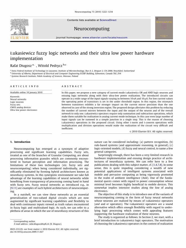
the chip area of the proposed circuit has been evaluated as afunction of the number of neurons (m) and the number of inputs(n) in the network. The results are shown in Fig. 13.
The presented results have been obtained on the basis of thenumber of transistors in the network, as a function of the n andthe m variables. Since the digital blocks require only smalltransistors, while the analog blocks use larger transistor tominimize the mismatch problem described above, both types oftransistors have been counted separately and multiplied by areasfor particular types of transistors. Some area has been assumedfor the connecting paths between particular blocks in the chip.Finally, the obtained areas have been multiplied by a correctionfactor, which has been calculated on the basis of the projectsrealized earlier by the authors. The presented areas do not includethe adaptation mechanism, which is not within the scope of thispaper. Such mechanism has been designed by the authors inanother project i.e. the analog Kohonen neural network [5,13] andits area in CMOS 0.18mm technology equals 1000mm2. Thenumber of such blocks in the network proposed in this paper isequal to n �m. Fig. 13 shows that even in case of very advancedsystem with 20 neurons and 10 inputs the chip area will berelatively small and equal to c. 0.15 mm2 without the adaptationmechanism or c. 0.35 mm2 with the adaptation mechanism.
This is also worth noting that all the xi+wi signals are alwayscopied to comparators and to the network output using the PMOScurrent mirrors, while the reference current Iref always using theNMOS mirrors. If an offset in comparators occurs and this offsethas a similar value for all comparators, which is possible in acareful layout design, it can be compensated by adjustment of thevalue of reference current, which is an additional advantage here.
6. Conclusions
In this study, we have proposed the new ultra low powercircuit realization of or and the and Łukasiewicz operators used aslogic connectives in OR and AND neurons and neural networks. Inthe proposed circuits the error reduction for small signals areachieved by eliminating a chain of current mirrors between theinput and the output of the neurons. The simulation results showthat the circuits can operate with currents that are at the level of
single nAmps, which is an attractive feature especially for verylow power portable devices.
In the present work, we have not described the adaptationmechanism realized at the transistor level that would be suitablefor the proposed network. The implementation of such mechan-ism becomes the problem by itself. We have proposed themechanism of this nature earlier when dealing with analogKohonen self organized feature maps [5,13]. After some modifica-tions, this mechanism can be adopted for the proposed network.
The implementation of the bias term, as described in Section 2,has not been discussed here but it can be easily realized inhardware, by simple addition of a single branch at the output ofeach neuron in the network.
References
[1] C.-Y. Chen, Y.-T. Hsieh, B.-D. Liu, Circuit implementation of linguistic-hedgefuzzy logic controller in current-mode approach, IEEE Transactions on FuzzySystems 11 (5) (2003) 624–646.
[2] M. Conti, G.D. Betta, S. Orcioni, G. Soncini, C. Turchetti, N. Zorzi, Test structurefor mismatch characterization of MOS transistors in subthreshold regime,IEEE International Conference on Microelectronic Test Structures 10 (1997)173–178.
[3] J.A. Croon, M. Rosmeulen, S. Decoutere, W. Sansen, H.E. Maes, An Easy-to-Usemismatch model for the MOS transistor, IEEE Journal of Solid-State Circuits37 (8) (2002) 1056–1064.
[4] E. Farshidi, A low-power current-mode defuzzifier for fuzzy logic controllers,International Conference on Signals, Circuits and Systems (SCS) (2008) 1–4.
[5] R. D"ugosz, T. Talaska, J. Dalecki, R. Wojtyna, Experimental Kohonen neuralnetwork implemented in CMOS 0.18mm technology, in: 15th InternationalConference Mixed Design of Integrated Circuits and Systems (MIXDES),Poznan, Poland, 2008, pp. 243–248.
[6] J. Jang, C. Sun, E. Mizutani, Neuro-Fuzzy and Soft Computing, Prentice Hall,Upper Saddle River, NJ, 1997.
[7] J.W. Mills, Area-efficient implication circuits for very dense Lukasiewicz logicarrays, International Symposium on Multiple-Valued Logic, 1992, pp. 291–298.
[8] A. Morgul, T. Temel, Current-mode level restoration: circuit for multi-valuedlogic, Electronics Letters 41 (5) (2005) 230–231.
[9] W. Pedrycz, Fuzzy neural networks and neurocomputations, Fuzzy Sets andSystems 56 (1993) 1–28.
[10] W. Pedrycz, Heterogeneous fuzzy logic networks: fundamentals and devel-opment studies, IEEE Transactions on Neural Networks 15 (2004) 1466–1481.
[11] W. Pedrycz, A. Rocha, Knowledge-based neural networks, IEEE Transactionson Fuzzy Systems 1 (1993) 254–266.
[12] A. Rodriguez-Vazquez, R. Navas, M. Delgado-Restituto, F. Vidal-Verdu, Amodular programmable CMOS analog fuzzy controller chip, IEEE Transactions

ARTICLE IN PRESS
R. D!ugosz, W. Pedrycz / Neurocomputing 73 (2010) 1222–12341234
on Circuits and Systems II: Analog and Digital Signal Processing 46 (3) (1999)251–265.
[13] T. Talaska, R. D"ugosz, W. Pedrycz, Adaptive weight change mechanism forKohonens’s neural network implemented in CMOS 0.18mm technology, in:11th European Symposium on Artificial Neural Networks, Bruges, Belgium,2007, pp. 151–156.
[14] J.X. Xu, C. Xue, C.C. Hang, K.V. Palem, A fuzzy control chip based onprobabilistic CMOS technology, IEEE International Conference on FuzzySystems FUZZ-IEEE (2008) 174–179.
[15] T. Yamakawa, T. Miki, The current mode fuzzy logic integrated circuitsfabricated by standard CMOS process, IEEE Transactions on Computers C 35(2) (1986) 161–167.
Rafa$ D$ugosz is currently with the Swiss FederalInstitute of Technology in Lausanne (EPFL) in Switzer-land, Institute of Microtechnology (IMT). He receivedM.Sc. in automatic and robotic in 1996 and Ph.D. intelecommunication in 2004 (with honours), both fromPoznan University of Technology (PUT) in Poland. From1996 to 2001 he was with the Institute of Electronicsand Telecommunication at PUT. From 2001 he is withDepartment of Computer Science and Management atPUT. He is the fellow of several scientific fellowshipsfrom Foundation for Polish Science in Poland (foryoung scientists and for young doctors) and from
European funds (Marie Curie Outgoing InternationalFellowship). Within these fellowships between 2005 and 2008 he was withDepartment of Electrical and Computer Engineering at the University of Alberta inCanada and since 2006 he holds the scientist position in EPFL. His main research
areas are ultra low power reconfigurable analog and mixed analog-digitalintegrated circuits such as analog finite impulse response filters, analog-to-digitalconverters and neural networks. Dr. D"ugosz has been involved in numerousprojects granted by EU and Polish Government. He has published over 80 researchpapers, including several book chapters.
Witold Pedrycz (M’88-SM’90-F’99) received the M.Sc.,and Ph.D., D.Sci. all from the Silesian University ofTechnology, Gliwice, Poland. He is a Professor andCanada Research Chair (CRC) in Computational Intelli-gence in the Department of Electrical and ComputerEngineering, University of Alberta, Edmonton, Canada.He is also with the Polish Academy of Sciences,Systems Research Institute, Warsaw, Poland.
His research interests encompass computationalintelligence, fuzzy modeling, knowledge discoveryand data mining, fuzzy control including fuzzy con-trollers, pattern recognition, knowledge-based neural
networks, granular and relational computing, andSoftware Engineering. He has published numerous papers in these areas. He isalso an author of 12 research monographs. Witold Pedrycz has been a member ofnumerous program committees of IEEE conferences in the area of fuzzy sets andneurocomputing. He serves as Editor-in-Chief of IEEE Transactions on SystemsMan and Cybernetics-part A and Associate Editor of IEEE Transactions on FuzzySystems. He is also an Editor-in-Chief of Information Sciences. Dr. Pedrycz is arecipient of the prestigious Norbert Wiener award from the IEEE Society ofSystems, Man, and Cybernetics and an IEEE Canada Silver Medal in ComputerEngineering.