Embed Size (px)
Citation preview
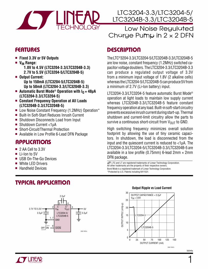
LTC3204-3.3/LTC3204-5/LTC3204B-3.3/LTC3204B-5
13204fa
FEATURES DESCRIPTIO
U
TYPICAL APPLICATIO
U
The LTC®3204-3.3/LTC3204-5/LTC3204B-3.3/LTC3204B-5 are low noise, constant frequency (1.2MHz) switched ca-pacitor voltage doublers. The LTC3204-3.3/LTC3204B-3.3 can produce a regulated output voltage of 3.3V from a minimum input voltage of 1.8V (2 alkaline cells) whereas the LTC3204-5/LTC3204B-5 can produce 5V from a minimum of 2.7V (Li-Ion battery) input.
LTC3204-3.3/LTC3204-5 feature automatic Burst Mode® operation at light loads to maintain low supply current whereas LTC3204B-3.3/LTC3204B-5 feature constant frequency operation at any load. Built-in soft-start circuitry prevents excessive inrush current during start-up. Thermal shutdown and current-limit circuitry allow the parts to survive a continuous short-circuit from VOUT to GND.
High switching frequency minimizes overall solution footprint by allowing the use of tiny ceramic capaci-tors. In shutdown, the load is disconnected from the input and the quiescent current is reduced to <1µA. The LTC3204-3.3/LTC3204-5/LTC3204B-3.3/LTC3204B-5 are available in a low profile (0.75mm) 6-lead 2mm × 2mm DFN package.
Low Noise Regulated Charge Pump in 2 × 2 DFN
Fixed 3.3V or 5V Outputs VIN Range:
1.8V to 4.5V (LTC3204-3.3/LTC3204B-3.3) 2.7V to 5.5V (LTC3204-5/LTC3204B-5)
Output Current: Up to 150mA (LTC3204-5/LTC3204B-5) Up to 50mA (LTC3204-3.3/LTC3204B-3.3)
Automatic Burst Mode® Operation with IQ = 48µA (LTC3204-3.3/LTC3204-5)
Constant Frequency Operation at All Loads (LTC3204B-3.3/LTC3204B-5)
Low Noise Constant Frequency (1.2MHz) Operation* Built-In Soft-Start Reduces Inrush Current Shutdown Disconnects Load from Input Shutdown Current <1µA Short-Circuit/Thermal Protection Available in Low Profile 6-Lead DFN Package
2 AA Cell to 3.3V Li-Ion to 5V USB On-The-Go Devices White LED Drivers Handheld Devices
Output Ripple vs Load Current
Burst Mode is a registered trademark of Linear Technology Corporation.*Protected by U.S. Patents including 6411531.
APPLICATIO SU
, LTC and LT are registered trademarks of Linear Technology Corporation.All other trademarks are the property of their respective owners.
OFF ON
VIN
GND
SHDN
VOUTC– C+
LTC3204-5/LTC3204B-5
2.2µF 2.2µF
2.2µF
5V2.7V TO 5.5V
3204 TA01a
1, 7
2 3
45
6
OUTPUT CURRENT (mA)0
0
OUTP
UT R
IPPL
E (m
Vp-p
)
5
10
15
20
30
25 50 75 100
3204 TA01b
125 150
25
OUTPUT CAPACITANCE = 2.2µFVIN = 3.6V
LTC3204B-5
LTC3204-5
LTC3204-3.3/LTC3204-5/LTC3204B-3.3/LTC3204B-5
23204fa
ABSOLUTE AXI U RATI GS
W WW U
FOR ATIOPACKAGE/ORDER IU UW
ELECTRICAL CHARACTERISTICS
SYMBOL PARAMETER CONDITIONS MIN TYP MAX UNITS
VIN Input Voltage Range (LTC3204-3.3/LTC3204B-3.3) 1.8 4.5 V (LTC3204-5/LTC3204B-5) 2.7 5.5 VVOUT Output Voltage Range 1.8V < VIN < 4.5V, IOUT < 40mA 1.9V < VIN < 4.5V, IOUT < 50mA (LTC3204-3.3/LTC3204B-3.3) 3.168 3.3 3.432 V 2.7V < VIN < 5.5V, IOUT < 65mA 3.1V < VIN < 5.5V, IOUT < 150mA (LTC3204-5/LTC3204B-5) 4.8 5 5.2 VIIN No Load Input Current IOUT = 0 (LTC3204-3.3) 48 µA IOUT = 0 (LTC3204-5) 60 µA IOUT = 0 (LTC3204B-3.3) 1.25 mA IOUT = 0 (LTC3204B-5) 3.6 mAISHDN Shutdown Current SHDN = 0V, VOUT = 0V 1 µAIBURST Burst Mode Threshold (LTC3204-3.3) 15 mA (LTC3204-5) 20 mAVR Output Ripple IOUT = 100mA 20 mVP-P
η Efficiency VIN = 3V, IOUT = 100mA (LTC3204-5/LTC3204B-5) 82 %fOSC Switching Frequency 0.6 1.2 1.8 MHzVIH SHDN Input Threshold 1.3 VVIL SHDN Input Threshold 0.4 VIIH SHDN Input Current –1 1 µAIIL SHDN Input Current SHDN = 0V –1 1 µAROL Effective Open-Loop Output VIN = 1.8V, VOUT = 3V (LTC3204-3.3/LTC3204B-3.3) 7 Ω Resistance (Note 3) VIN = 2.7V, VOUT = 4.5V (LTC3204-5/LTC3204B-5) 6 Ω
ILIM Output Current Limit VOUT = OV 300 mATSS Soft-Start Time From the Rising Edge of SHDN to 90% of VOUT 0.75 ms
VIN to GND ................................................... –0.3V to 6VVOUT to GND ............................................. –0.3V to 5.5VSHDN to GND ............................................... –0.3V to 6VVOUT Short-Circuit Duration ............................. IndefiniteOperating Temperature Range (Note 2) ...–40°C to 85°CStorage Temperature Range .................. –65°C to 125°CMaximum Junction Temperature .......................... 125°C
(Note 1)
The denotes the specifications which apply over the full operating temperature range. Specifications are at TA = 25°C, VIN = 2.4V (LTC3204-3.3/LTC3204B-3.3) or 3.6V (LTC3204-5/LTC3204B-5), SHDN = VIN, CFLY = 2.2µF, CIN = 2.2µF, COUT = 2.2µF unless otherwise noted.
Note 1: Absolute Maximum Ratings are those beyond which the life of a device may be impaired.Note 2: The LTC3204-3.3/LTC3204-5/LTC3204B-3.3/LTC3204B-5 are guaranteed to meet performance specifications from 0°C to 70°C.
Specifications over the –40°C to 85°C operating temperature range are assured by design, characterization and correlation with statistical process controls.Note 3: ROL ≡ (2VIN – VOUT)/IOUT
Consult LTC Marketing for parts specified with wider operating temperature ranges.
ORDER PART NUMBER
DC PART MARKING
LBJVLBNKLBVFLBVG
LTC3204EDC-3.3LTC3204EDC-5LTC3204BEDC-3.3LTC3204BEDC-5
TJMAX = 125°C, θJA = 80°C/WEXPOSED PAD IS GND (PIN 7)MUST BE SOLDERED TO PCB
TOP VIEW
DC PACKAGE6-LEAD (2mm × 2mm) PLASTIC DFN
4
5
6
7
3
2
1GND
VIN
VOUT
SHDN
C–
C+
LTC3204-3.3/LTC3204-5/LTC3204B-3.3/LTC3204B-5
33204fa
TYPICAL PERFOR
UW
CE CHARACTERISTICSA
TEMPERATURE (°C)–50 150
3204 G05
0 50 100TEMPERATURE (°C)
–50 1500 50 100
3204 G04
THRE
SHOL
D VO
LTAG
E (V
)
0.7
0.8
0.6
0.5
0.9
SHDN
THR
ESHO
LD L
O-TO
-HI (
V)
0.7
0.8
0.6
0.5
0.9
SHDN
THR
ESHO
LD H
I-TO-
LO (V
)
0.6
0.7
0.5
0.4
0.8
SUPPLY VOLTAGE (V)1.5
FREQ
UENC
Y (M
Hz)
1.50
1.25
1.00
0.75
0.50
0.25
02.0 2.5 3.0 3.5 4.0 4.5
3204 G01
SUPPLY VOLTAGE (V)1.5 2.0 2.5 3.0 3.5 4.0 4.5
3204 G03
TEMPERATURE (°C)–50
FREQ
UENC
Y (M
Hz)
1.4
1.3
1.2
1.1
1.0
0.9
0.8–20 10 40 70 100 130
3204 G02
SUPPLY VOLTAGE (V)
SHOR
T-CI
RCUI
T CU
RREN
T (m
A)
350
300
250
200
150
100
50
0
3204 G06
1.5 2.0 2.5 3.0 3.5 4.0 4.5
DEVICE CYCLES IN AND OUT OF
THERMAL SHUTDOWN
VIN = 4.5V
HIGH-TO-LOW THRESHOLD
LOW-TO-HIGH THRESHOLD
VIN = 3.2V
VIN = 3.2V
VIN = 1.8V VIN = 1.8V
VIN = 2.4V
VIN = 1.8V
VIN = 2.4V
VIN = 2.4V
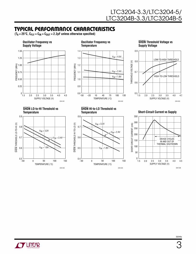
Oscillator Frequency vs Supply Voltage
Oscillator Frequency vs Temperature
SHDN Threshold Voltage vs Supply Voltage
Short-Circuit Current vs Supply
(TA = 25°C, CFLY = CIN = COUT = 2.2µF unless otherwise specified)
S HDN LO-to-HI Threshold vs Temperature
SHDN HI-to-LO Threshold vs Temperature
LTC3204-3.3/LTC3204-5/LTC3204B-3.3/LTC3204B-5
43204fa
SUPPLY VOLTAGE (V)1.8
EFFI
CIEN
CY (%
)
100
90
80
70
60
50
40
30
20
10
02.2 2.6 2.82.0 2.4 3.0 3.2
TEMPERATURE (°C)–50 0 50 100
6
7
5
9
3204 G09
VIN = 1.8VVOUT = 3V
3204 G12
3204 G143204 G13 3204 G15
3204 G07
SUPPLY VOLTAGE (V)
LOAD
CUR
RENT
(mA)
400
350
300
250
200
150
100
50
0
3204 G08
1.5 2.0 2.5 3.0 3.5
8
IOUT = 1mA
THEORETICAL MAX
IOUT = 30mA
LOAD CURRENT (mA)0
OUTP
UT V
OLTA
GE (V
)
3.35
3.30
3.25
3.20
3.15
3.10
3.05100 200 300 400 500
VIN = 1.8V
VIN = 2.4V
VIN = 3.2V
VOUT = 3.168V
TA = 25°C
TA = 90°C
TA = –45°C
SUPPLY VOLTAGE (V)1.8
44
NO-L
OAD
INPU
T CU
RREN
T (µ
A)
NO-LOAD INPUT CURRENT (mA)
46
50
52
54
64
58
2.2 2.6 2.8
3204 G10
48
60
62
56
0
0.2
0.6
0.8
1.0
2.0
1.4
0.4
1.6
1.8
1.2
2 2.4 3 3.2
LTC3204B-3.3
LTC3204-3.3
LOAD CURRENT (mA)
0.01
0.1
EXCE
SS IN
PUT
CURR
ENT
(mA)
1
0.01 0.1 1 10 100
3204 G11
10
1000
LTC3204B-3.3(NON-BURST MODEOPERATION)
LTC3204-3.3(BURST MODEOPERATION)
VIN = 2.4V
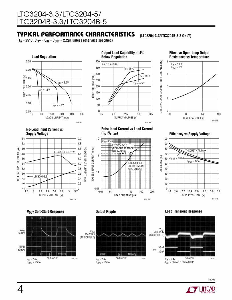
VOUT Soft-Start Response Output Ripple Load Transient Response
No-Load Input Current vs Supply Voltage
Extra Input Current vs Load Current (IIN-2ILOAD)
Effective Open-Loop Output Resistance vs Temperature
(TA = 25°C, CFLY = CIN = COUT = 2.2µF unless otherwise specified)
Load RegulationOutput Load Capability at 4% Below Regulation
(LTC3204-3.3/LTC3204B-3.3 ONLY)
VOUT20mV/DIV
(AC COUPLED)
IOUT50mA
30mA
10µs/DIV
VOUT2V/DIV
SHDN2V/DIV
500µs/DIV
VOUT20mV/DIV
(AC COUPLED)
500ns/DIVVIN = 2.4VILOAD = 50mA
VIN = 2.4VILOAD = 50mA
VIN = 2.4VIOUT = 30mA TO 50mA STEP
3204 G13 3204 G14 3204 G15
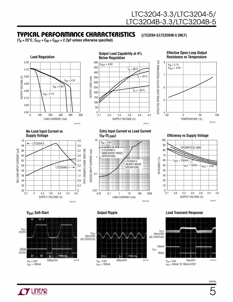
Efficiency vs Supply Voltage
TYPICAL PERFOR A CE CHARACTERISTICS
UW
LTC3204-3.3/LTC3204-5/LTC3204B-3.3/LTC3204B-5
53204fa
2.7 4.53.0 3.3 3.6 3.9 4.2
3204 G18
3204 G21
3204 G233204 G22 3204 G24
3204 G16 3204 G17
SUPPLY VOLTAGE (V)2.7
OUTP
UT L
OAD
(mA)
3.93.0 3.3 3.6 4.2
500
450
400
350
300
250
200
150
100
50
0
TEMPERATURE (°C)1000 50
VIN = 2.7VVOUT = 4.5V
VOUT = 4.8V
LOAD CURRENT (mA)0
5.20
5.10
5.00
4.90
4.80
4.70
4.60
4.50300100 200 400 500
OUTP
UT V
OLTA
GE (V
)
VIN = 4.2V
VIN = 2.7V
VIN = 3.6V
SUPPLY VOLTAGE (V)
EFFI
CIEN
CY (%
)
100
90
80
70
60
50
40
30
20
10
0
IOUT = 1mA
THEORETICAL MAX
IOUT = 10mA
IOUT = 100mA
–50
8
7
6
5
4
TA = 25°C
TA = 90°C
TA = –45°C
SUPPLY VOLTAGE (V)2.7
50
NO-L
OAD
INPU
T CU
RREN
T (µ
A)
NO-LOAD INPUT CURRENT (mA)54
58
62
3 3.3 3.6 3.9
3204 G19
4.2
66
70
52
56
60
64
68
0
0.8
1.6
2.4
3.2
4.0
0.4
1.2
2.0
2.8
3.6
4.5
LTC3204B-5
LTC3204-5
LOAD CURRENT (mA)
0.01
0.1
EXCE
SS IN
PUT
CURR
ENT
(mA)
1
0.01 0.1 1 10 100
3204 G20
10
1000
LTC3204B-5(N0N-BURST MODEOPERATION)
LTC3204-5(BURST-MODEOPERATION)
VIN = 3.6V
Load RegulationOutput Load Capability at 4% Below Regulation
Effective Open-Loop Output Resistance vs Temperature
VOUT Soft-Start Output Ripple Load Transient Response
No-Load Input Current vs Supply Voltage Efficiency vs Supply Voltage
Extra Input Current vs Load Current (IIN-2ILOAD)
(TA = 25°C, CFLY = CIN = COUT = 2.2µF unless otherwise specified)(LTC3204-5/LTC3204B-5 ONLY)
VOUT50mV/DIV
(AC COUPLED)
IOUT100mA
60mA
10µs/DIV
VOUT2V/DIV
SHDN5V/DIV
500µs/DIV
VOUT20mV/DIV
(AC COUPLED)
500ns/DIVVIN = 3.6VIOUT = 100mA
VIN = 3.6VIOUT = 100mA
VIN = 3.6VIOUT = 60mA TO 100mA STEP
TYPICAL PERFOR A CE CHARACTERISTICS
UW
LTC3204-3.3/LTC3204-5/LTC3204B-3.3/LTC3204B-5
63204fa
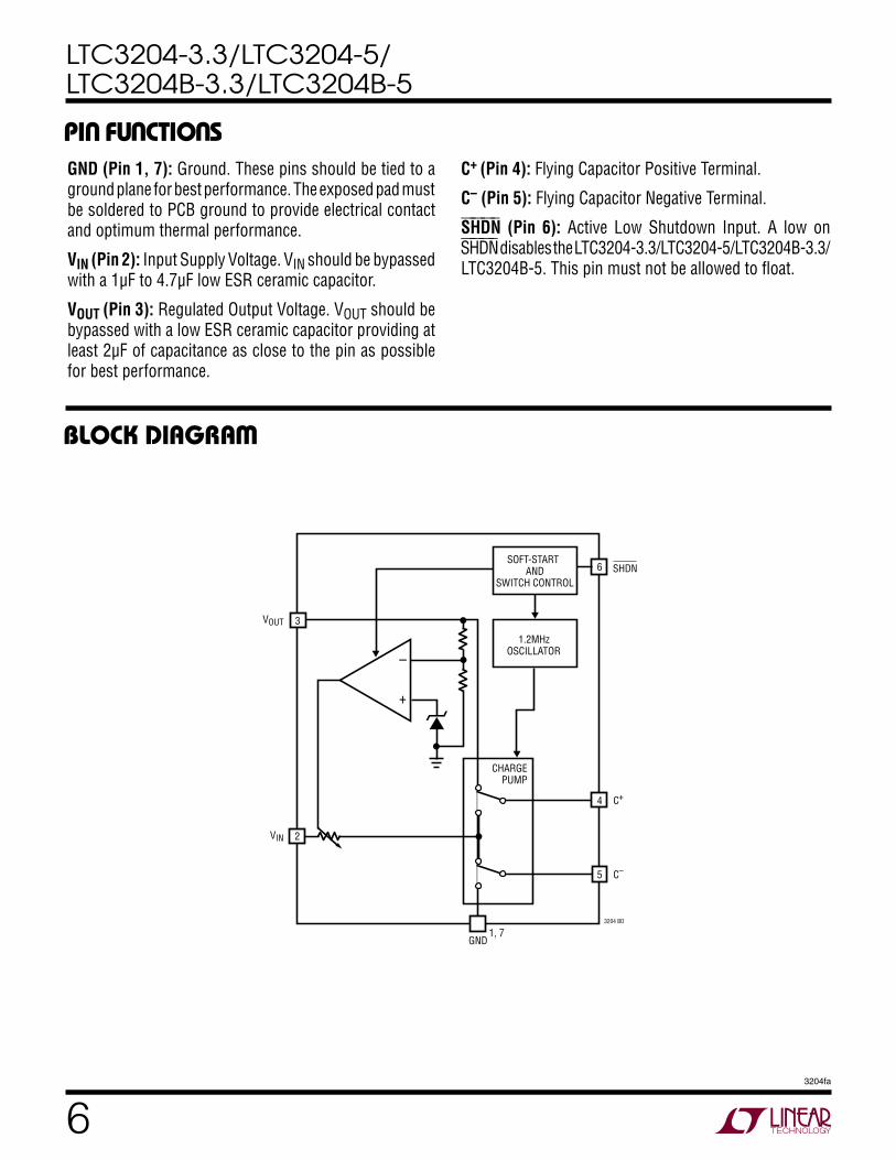
GND (Pin 1, 7): Ground. These pins should be tied to a ground plane for best performance. The exposed pad must be soldered to PCB ground to provide electrical contact and optimum thermal performance.
VIN (Pin 2): Input Supply Voltage. VIN should be bypassed with a 1µF to 4.7µF low ESR ceramic capacitor.
VOUT (Pin 3): Regulated Output Voltage. VOUT should be bypassed with a low ESR ceramic capacitor providing at least 2µF of capacitance as close to the pin as possible for best performance.
C+ (Pin 4): Flying Capacitor Positive Terminal.
C– (Pin 5): Flying Capacitor Negative Terminal.
SHDN (Pin 6): Active Low Shutdown Input. A low on SHDN disables the LTC3204-3.3/LTC3204-5/LTC3204B-3.3/ LTC3204B-5. This pin must not be allowed to float.
–
+
VOUT
VIN
SHDN
C+
C–
3204 BD
CHARGEPUMP
1.2MHzOSCILLATOR
SOFT-START AND
SWITCH CONTROL
GND
5
4
1, 7
2
3
6
UUU
PI FU CTIO S
BLOCK DIAGRA
W
LTC3204-3.3/LTC3204-5/LTC3204B-3.3/LTC3204B-5
73204fa
The LTC3204-3.3/LTC3204-5/LTC3204B-3.3/LTC3204B-5 use a switched capacitor charge pump to boost VIN to a regulated output voltage. Regulation is achieved by sensing the output voltage through an internal resistor divider and modulating the charge pump output current based on the error signal. A 2-phase nonoverlapping clock activates the charge pump switches. The flying capacitor is charged from VIN on the first phase of the clock. On the second phase of the clock it is stacked in series with VIN and connected to VOUT. This sequence of charging and discharging the flying capacitor continues at a free running frequency of 1.2MHz (typ).
Shutdown Mode
In shutdown mode, all circuitry is turned off and the LTC3204-3.3/LTC3204-5/LTC3204B-3.3/LTC3204B-5 draws only leakage current from the VIN supply. Further-more, VOUT is disconnected from VIN. The SHDN pin is a CMOS input with a threshold voltage of approximately 0.7V. The LTC3204-3.3/LTC3204-5/LTC3204B-3.3/LTC3204B-5 are in shutdown when a logic low is applied to the SHDN pin. Since the SHDN pin is a very high impedance CMOS input, it should never be allowed to float. To ensure that its state is defined, it must always be driven with a valid logic level.
Since the output voltages of these devices can go above the input voltage, special circuitry is required to control the internal logic. Detection logic will draw an input current of 5µA when the devices are in shutdown. However, this current will be eliminated if the output voltage (VOUT) is less than approximately 0.8V.
Burst Mode Operation
The LTC3204-3.3/LTC3204-5 provide automatic Burst Mode operation to reduce supply current at light loads. Burst Mode operation is initiated if the output load current falls below an internally programmed threshold. Once
(Refer to the Block Diagram)
Burst Mode operation is initiated, the part shuts down the internal oscillator to reduce the switching losses and goes into a low current state. This state is referred to as the sleep state in which the IC consumes only about 40µA from the input. When the output voltage droops enough to overcome the burst comparator hysteresis, the part wakes up and commences normal fixed frequency opera-tion. The output capacitor recharges and causes the part to reenter the sleep state if the output load still remains less than the Burst Mode threshold. This Burst Mode threshold varies with VIN, VOUT and the choice of output storage capacitor.
Soft-Start
The LTC3204-3.3/LTC3204-5/LTC3204B-3.3/LTC3204B-5 have built-in soft-start circuitry to prevent excessive current flow during start-up. The soft-start is achieved by charging an internal capacitor with a very weak current source. The voltage on this capacitor, in turn, slowly ramps the amount of current available to the output storage capacitor from zero to a value of 300mA over a period of approximately 0.75ms. The soft-start circuit is reset in the event of a commanded shutdown or thermal shutdown.
Short-Circuit/Thermal Protection
The LTC3204-3.3/LTC3204-5/LTC3204B-3.3/LTC3204B-5 have built-in short-circuit current limit as well as over-tem-perature protection. During a short-circuit condition, they will automatically limit their output current to approximately 300mA. At higher temperatures, or if the input voltage is high enough to cause excessive self-heating of the part, the thermal shutdown circuitry will shutdown the charge pump once the junction temperature exceeds approximately 160°C. It will enable the charge pump once the junction temperature drops back to approximately 150°C. The LTC3204-3.3/LTC3204-5/LTC3204B-3.3/LTC3204B-5 will cycle in and out of thermal shutdown indefinitely without latchup or damage until the short-circuit condition on VOUT is removed.
OPERATIOU
LTC3204-3.3/LTC3204-5/LTC3204B-3.3/LTC3204B-5
83204fa
Power Efficiency
The power efficiency (η) of the LTC3204-3.3/LTC3204-5/ LTC3204B-3.3/LTC3204B-5 is similar to that of a linear regulator with an effective input voltage of twice the actual input voltage. This occurs because the input current for a voltage doubling charge pump is approximately twice the output current. In an ideal regulating voltage doubler the power efficiency would be given by:
η = = =P
PV IV I
VV
OUT
IN
OUT OUT
IN OUT
OUT
IN
••2 2
At moderate to high output power, the switching losses and the quiescent current of the LTC3204-3.3/LTC3204-5/ LTC3204B-3.3/LTC3204B-5 are negligible and the expres-sion above is valid. For example, with VIN = 3V, IOUT = 100mA and VOUT regulating to 5V, the measured efficiency is 81.8% which is in close agreement with the theoretical 83.3% calculation.
Maximum Available Output Current
For the LTC3204-3.3/LTC3204-5/LTC3204B-3.3/ LTC3204B-5,the maximum available output current and voltage can be calculated from the effective open-loop output resistance, ROL, and the effective input voltage, 2VIN(MIN).
(fOSC), value of the flying capacitor (CFLY), the nonoverlap time, the internal switch resistances (RS), and the ESR of the external capacitors. A first order approximation for ROL is given below:
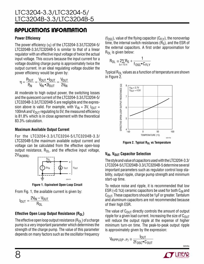
R R
f COL SOSC FLY
≅ ∑ +21•
Typical ROL values as a function of temperature are shown in Figure 2.
Figure 1. Equivalent Open-Loop Circuit
From Fig. 1, the available current is given by:
I
V VROUT
IN OUT
OL= 2 –
Effective Open Loop Output Resistance (ROL)
The effective open loop output resistance (ROL) of a charge pump is a very important parameter which determines the strength of the charge pump. The value of this parameter depends on many factors such as the oscillator frequency
Figure 2. Typical ROL vs Temperature
VIN, VOUT Capacitor Selection
The style and value of capacitors used with the LTC3204-3.3/ LTC3204-5/LTC3204B-3.3/LTC3204B-5 determine several important parameters such as regulator control loop sta-bility, output ripple, charge pump strength and minimum start-up time.
To reduce noise and ripple, it is recommended that low ESR (<0.1Ω) ceramic capacitors be used for both CIN and COUT. These capacitors should be 1µF or greater. Tantalum and aluminum capacitors are not recommended because of their high ESR.
The value of COUT directly controls the amount of output ripple for a given load current. Increasing the size of COUT will reduce the output ripple at the expense of higher minimum turn-on time. The peak-to-peak output ripple is approximately given by the expression:
V
If CRIPPLE P P
OUT
OSC OUT( ) •− ≅
2
+–
ROL
IOUT VOUT2VIN
3204 F01
+
–
S=1 TO 4
APPLICATIO S I FOR ATIO
WU UU
3204 F02
TEMPERATURE (°C)1000 50
EFFE
CTIV
E OP
EN-L
OOP
OUTP
UT R
ESIS
TANC
E (Ω
)
VIN = 2.7VVOUT = 4.5V
–50
8
7
6
5
4
LTC3204-3.3/LTC3204-5/LTC3204B-3.3/LTC3204B-5
93204fa
where fOSC is the oscillator frequency (typically 1.2MHz) and COUT is the value of output charge storage capacitor.
Also, the value and style of the output capacitor can signifi-cantly affect the stability of the LTC3204-3.3/LTC3204-5/ LTC3204B-3.3/LTC3204B-5. As shown in the Block Diagram, the LTC3204-3.3/LTC3204-5/LTC3204B-3.3/LTC3204B-5 use a linear control loop to adjust the strength of the charge pump to match the current required at the output. The error signal of this loop is stored directly on the output storage capacitor. This out-put capacitor also serves to form the dominant pole of the control loop. To prevent ringing or instability on the LTC3204-3.3/LTC3204-5/LTC3204B-3.3/LTC3204B-5, it is important to maintain at least 1µF of capacitance over all conditions.
Excessive ESR on the output capacitor can degrade the loop stability of the LTC3204-3.3/LTC3204-5/LTC3204B-3.3/ LTC3204B-5. The closed loop output resistance of the LTC3204-5 is designed to be 0.5Ω. For a 100mA load current change, the output voltage will change by about 50mV. If the output capacitor has 0.5Ω or more of ESR, the closed loop frequency response will cease to roll off in a simple one-pole fashion and poor load transient response or instability could result. Ceramic capacitors typically have exceptional ESR performance and combined with a good board layout should yield very good stability and load transient performance.
As the value of COUT controls the amount of output ripple, the value of CIN controls the amount of ripple present at the input pin (VIN). The input current to the LTC3204-3.3/LTC3204-5/LTC3204B-3.3/LTC3204B-5 will be relatively constant during the input charging phase or the output charging phase but will drop to zero during the nonoverlap times. Since the nonoverlap time is small (~25ns), these missing notches will result in only a small perturbation on the input power supply line. Note that a higher ESR capacitor such as tantalum will have higher input noise due to the voltage drop in the ESR. Therefore, ceramic capacitors are again recommended for their exceptional ESR performance.
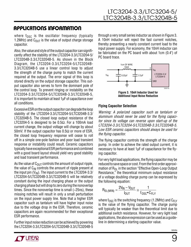
Further input noise reduction can be achieved by powering the LTC3204-3.3/LTC3204-5/LTC3204B-3.3/LTC3204B-5
through a very small series inductor as shown in Figure 3. A 10nH inductor will reject the fast current notches, thereby presenting a nearly constant current load to the input power supply. For economy, the 10nH inductor can be fabricated on the PC board with about 1cm (0.4") of PC board trace.
Figure 3. 10nH Inductor Used forAdditional Input Noise Reduction
Flying Capacitor Selection
Warning: A polarized capacitor such as tantalum or aluminum should never be used for the flying capaci-tor since its voltage can reverse upon start-up of the LTC3204-3.3/LTC3204-5/LTC3204B-3.3/LTC3204B-5. Low ESR ceramic capacitors should always be used for the flying capacitor.
The flying capacitor controls the strength of the charge pump. In order to achieve the rated output current, it is necessary to have at least 1µF of capacitance for the fly-ing capacitor.
For very light load applications, the flying capacitor may be reduced to save space or cost. From the first order approxi-mation of ROL in the section “Effective Open-Loop Output Resistance,” the theoretical minimum output resistance of a voltage doubling charge pump can be expressed by the following equation:
R
V VI f CL MIN
IN OUT
OUT OSC FLY0
2 1( )
–•
= ≅
where fOSC is the switching frequency (1.2MHz) and CFLY is the value of the flying capacitor. The charge pump will typically be weaker than the theoretical limit due to additional switch resistance. However, for very light load applications, the above expression can be used as a guide-line in determining a starting capacitor value.
LTC3204-3.3/LTC3204-50.22µF 2.2µF
VIN
GND
1cm OF WIRE10nH
VIN
1
2
32005 F03
APPLICATIO S I FOR ATIO
WU UU

LTC3204-3.3/LTC3204-5/LTC3204B-3.3/LTC3204B-5
103204fa
COUT0603
CIN0603
CFLY0603
GND
VOUT
VIN
3204 F04
SHDN
C+
C–
Ceramic Capacitors
Ceramic capacitors of different materials lose their capaci-tance with higher temperature and voltage at different rates. For example, a capacitor made of X5R or X7R material will retain most of its capacitance from –40°C to 85°C whereas a Z5U or Y5V style capacitor will lose considerable capacitance over that range. Z5U and Y5V capacitors may also have a poor voltage coefficient causing them to lose 60% or more of their capacitance when the rated voltage is applied. Therefore when comparing different capacitors, it is often more appropriate to compare the amount of achievable capacitance for a given case size rather than discussing the specified capacitance value. For example, over rated voltage and temperature conditions, a 1µF 10V Y5V ceramic capacitor in a 0603 case may not provide any more capacitance than a 0.22µF 10V X7R capacitor avail-able in the same 0603 case. In fact, for most LTC3204-3.3/ LTC3204-5/LTC3204B-3.3/LTC3204B-5 applications, these capacitors can be considered roughly equivalent. The capacitor manufacturer’s data sheet should be consulted to ensure the desired capacitance at all temperatures and voltages.
Below is a list of ceramic capacitor manufacturers and how to contact them: AVX www.avxcorp.com Kemet www.kemet.com Murata www.murata.com Taiyo Yuden www.t-yuden.com Vishay www.vishay.com TDK www.component.tdk.com
Layout Considerations
Due to the high switching frequency and high transient currents produced by LTC3204-3.3/LTC3204-5/LTC3204B-3.3/LTC3204B-5, careful board layout is necessary for optimum performance. A true ground plane and short connections to all the external capacitors will improve per-formance and ensure proper regulation under all conditions. Figure 4 shows an example layout for the LTC3204-3.3/ LTC3204-5/LTC3204B-3.3/LTC3204B-5.
Thermal Management
For higher input voltages and maximum output cur-rent, there can be substantial power dissipation in the LTC3204-3.3/LTC3204-5/LTC3204B-3.3/LTC3204B-5. If the junction temperature increases above approximately 160°C, the thermal shutdown circuitry will automatically deactivate the output. To reduce the maximum junction temperature, a good thermal connection to the PC board is recommended. Connecting the GND pin (Pin 1) and the exposed pad of the DFN package (Pin 7) to a ground plane under the device on two layers of the PC board can reduce the thermal resistance of the package and PC board considerably.
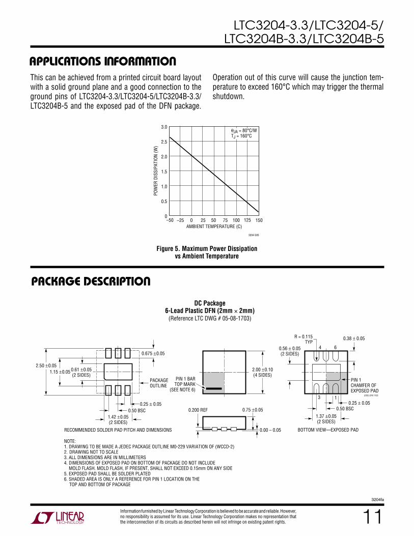
Derating Power at High Temperatures
To prevent an overtemperature condition in high power applications, Figure 5 should be used to determine the maximum combination of ambient temperature and power dissipation.
The power dissipated in the LTC3204-3.3/LTC3204-5/LTC3204B-3.3/LTC3204B-5 should always fall under the line shown for a given ambient temperature. The power dissipation in the LTC3204-3.3/ LTC3204-5/LTC3204B-3.3/ LTC3204B-5 is given by the expression:
P V V ID IN OUT OUT= ( – )•2
This derating curve assumes a maximum thermal resis-tance, θJA, of 80°C/W for the 2mm × 2mm DFN package.
Figure 4. Recommended Layout
APPLICATIO S I FOR ATIO
WU UU
LTC3204-3.3/LTC3204-5/LTC3204B-3.3/LTC3204B-5
113204fa
PACKAGE DESCRIPTIO
U
This can be achieved from a printed circuit board layout with a solid ground plane and a good connection to the ground pins of LTC3204-3.3/LTC3204-5/LTC3204B-3.3/LTC3204B-5 and the exposed pad of the DFN package.
Figure 5. Maximum Power Dissipation vs Ambient Temperature
Operation out of this curve will cause the junction tem-perature to exceed 160°C which may trigger the thermal shutdown.
AMBIENT TEMPERATURE (C)
POW
ER D
ISSI
PATI
ON (W
)
3204 G05
3.0
2.5
2.0
1.5
1.0
0.5
0–50 0 50 75–25 25 100 125 150
DC Package6-Lead Plastic DFN (2mm × 2mm)
(Reference LTC DWG # 05-08-1703)
2.00 ±0.10(4 SIDES)
NOTE:1. DRAWING TO BE MADE A JEDEC PACKAGE OUTLINE M0-229 VARIATION OF (WCCD-2)2. DRAWING NOT TO SCALE3. ALL DIMENSIONS ARE IN MILLIMETERS4. DIMENSIONS OF EXPOSED PAD ON BOTTOM OF PACKAGE DO NOT INCLUDE MOLD FLASH. MOLD FLASH, IF PRESENT, SHALL NOT EXCEED 0.15mm ON ANY SIDE5. EXPOSED PAD SHALL BE SOLDER PLATED 6. SHADED AREA IS ONLY A REFERENCE FOR PIN 1 LOCATION ON THE
TOP AND BOTTOM OF PACKAGE
0.38 ± 0.05
BOTTOM VIEW—EXPOSED PAD
0.56 ± 0.05(2 SIDES)
0.75 ±0.05
R = 0.115TYP
1.37 ±0.05(2 SIDES)
13
64
PIN 1 BARTOP MARK
(SEE NOTE 6)
0.200 REF
0.00 – 0.05
(DC6) DFN 1103
0.25 ± 0.05
1.42 ±0.05(2 SIDES)
RECOMMENDED SOLDER PAD PITCH AND DIMENSIONS
0.61 ±0.05(2 SIDES)
1.15 ±0.05
0.675 ±0.05
2.50 ±0.05
PACKAGEOUTLINE
0.25 ± 0.050.50 BSC0.50 BSC
PIN 1CHAMFER OFEXPOSED PAD
Information furnished by Linear Technology Corporation is believed to be accurate and reliable. However, no responsibility is assumed for its use. Linear Technology Corporation makes no representation that the interconnection of its circuits as described herein will not infringe on existing patent rights.
APPLICATIO S I FOR ATIO
WU UU
LTC3204-3.3/LTC3204-5/LTC3204B-3.3/LTC3204B-5
123204fa
Linear Technology Corporation1630 McCarthy Blvd., Milpitas, CA 95035-7417 (408) 432-1900 FAX: (408) 434-0507 www.linear.com LINEAR TECHNOLOGY CORPORATION 2004
LT/LT 0605 • PRINTED IN USA
RELATED PARTS
2
5 4
LTC3204-5
2.2µF
2.2µF2.2µF 6
3
1, 7
32005 TA05
VOUT5V ±4%
C– C+
VIN VOUT
GNDSHDN
Regulated 3.3V Output
Lithium-Ion Battery to 5V White or Blue LED Driver
USB Port to Regulated 5V Power Supply
PART NUMBER DESCRIPTION COMMENTS
LTC1751-3.3/ 100mA, 800kHz Regulated Doubler VIN: 2V to 5V, VOUT(MAX) = 3.3V/5V, IQ = 20µA, LTC1751-5 ISD <2µA, MS8 PackageLTC1983-3/ 100mA, 900kHz Regulated Inverter VIN: 3.3V to 5.5V, VOUT(MAX) = –3V/–5V, IQ = 25µA, LTC1983-5 ISD <1µA, ThinSOT PackageLTC3200-5 100mA, 2MHz Low Noise, Doubler/ VIN: 2.7V to 4.5V, VOUT(MAX) = 5V, IQ = 3.5mA, White LED Driver ISD <1µA, ThinSOT PackageLTC3202 125mA, 1.5MHz Low Noise, Fractional VIN: 2.7V to 4.5V, VOUT(MAX) = 5.5V, IQ = 2.5mA, White LED Driver ISD <1µA, DFN, MS Packages
TYPICAL APPLICATIO S
U
3V TO 4.4VLi-Ion
BATTERY
C– C+
VIN
5 4
VOUT
LTC3204-5/LTC3204B-5
GNDSHDN
3
1, 7
2
2.2µF
6
2.2µF 2.2µF
3200-5 TA03
DRIVE UP TO 5 LEDS
ON OFF
VSHDN(APPLY PWM WAVEFORM FOR
ADJUSTABLE BRIGHTNESS CONTROL) t
100Ω 100Ω 100Ω 100Ω 100Ω
OFF ON
VIN
GND
SHDN
VOUTVOUT3.3V
C– C+
LTC3204-3.3/LTC3204B-3.3
2.2µF 2.2µF
2.2µF
VIN1.8V TO 4.5V
3204 TA02
1, 7
2 3
45
6


![profdoc.um.ac.irprofdoc.um.ac.ir/articles/a/1023326.pdf · AISC-ASD89 3.3 , FEMA356 e J B- 3.3 3.3 I' 3.3 GAP b X.Þ 4.' . [P] .( (opening) L I' 3.3 3.3 3.3 " 4.' 3.3 01.4' 3.3 Gap](https://img.dokumen.tips/doc/110x75/605cbeefadb60b3eef7845e5/aisc-asd89-33-fema356-e-j-b-33-33-i-33-gap-b-x-4-p-opening.jpg)