Embed Size (px)
Citation preview
Low Voltage Intel® Pentium® III Processor with 512KB L2 Cache
Datasheet
Product Features
The LV Intel® Pentium® III processor 512K is designed for high-performance computing applications. It is binary compatible with previous Intel Architecture processors. The processor provides great performance for applications that run on advanced operating systems such as Microsoft* Windows* NT, Microsoft Windows 2000, Microsoft Windows XP and Linux. This is achieved by integrating the best attributes of Intel processors—the dynamic execution, Dual Independent Bus architecture plus Intel® MMX™ technology, and Internet Streaming SIMD Extensions—to bring a new level of performance to system designs. The LV Intel Pentium III processor with 512 Kbytes of L2 cache extends the power of the Intel Pentium III processor with performance headroom for applied computing and communications applications, and for high density Web serving and other front-end operations. Systems based on the LV Intel Pentium III Processor 512K also include the latest features to simplify system management and lower the cost of ownership.
Available at 800, 933, and 1000 MHz with a 133 MHz system bus frequency at 1.15 V (LV)
512-Kbyte Advanced Transfer Cache (on-die, full speed level two (L2) cache with Error Correcting Code (ECC))
Dual Independent Bus (DIB) architecture: separate dedicated external system bus and dedicated internal high-speed cache bus
Internet Streaming SIMD Extensions for enhanced video, sound and 3D performance
Binary compatible with applications running on previous members of the Intel microprocessor line
Dynamic execution micro architecture Power Management capabilities
—System Management mode—Multiple low-power states
Optimized for 32-bit applications running on advanced 32-bit operating systems
Micro-FCBGA packaging technology—Supports small form factor designs—Exposed die enables more efficient heat
dissipation Integrated high performance 16 Kbyte
instruction and 16 Kbyte data, nonblocking, level one cache
Quad Quadword Wide (256-bit) cache data bus provides extremely high throughput on read/store operations
8-way cache associativity provides improved cache hit rate on reads/store operations
Error-correcting code for system bus data Dual processor capable
Order Number: 273673-005Jan 2003
2
Information in this dproperty rights is grwhatsoever, and Intfitness for a particulintended for use in
Intel may make cha
Designers must notfuture definition and
The Low Voltage Inpublished specifica
MPEG is an internaplatforms may requ
Contact your local I
Copies of documen1-800-548-4725 or
Copyright © Intel C
AlertVIEW, i960, AnDM3, EtherExpressIntelDX2, IntelDX4,NetBurst, Intel NetSIntel WebOutfitter, Ilogo, OverDrive, PaRemoteExpress, ScTokenExpress, Trilliother countries.
*Other names and b
®
Datasheet
ocument is provided in connection with Intel products. No license, express or implied, by estoppel or otherwise, to any intellectual anted by this document. Except as provided in Intel's Terms and Conditions of Sale for such products, Intel assumes no liability el disclaims any express or implied warranty, relating to sale and/or use of Intel products including liability or warranties relating to ar purpose, merchantability, or infringement of any patent, copyright or other intellectual property right. Intel products are not medical, life saving, or life sustaining applications.
nges to specifications and product descriptions at any time, without notice.
rely on the absence or characteristics of any features or instructions marked “reserved” or “undefined.” Intel reserves these for shall have no responsibility whatsoever for conflicts or incompatibilities arising from future changes to them.
tel® Pentium® III processor 512K may contain design defects or errors known as errata that may cause the product to deviate from tions. Current characterized errata are available on request.
tional standard for video compression/decompression promoted by ISO. Implementations of MPEG CODECs, or MPEG enabled ire licenses from various entities, including Intel Corporation.
ntel sales office or your distributor to obtain the latest specifications and before placing your product order.
ts that have an ordering number and are referenced in this document, or other Intel literature may be obtained by calling by visiting Intel's website at http://www.intel.com.
orporation, 2003
yPoint, AppChoice, BoardWatch, BunnyPeople, CablePort, Celeron, Chips, Commerce Cart, CT Connect, CT Media, Dialogic, , ETOX, FlashFile, GatherRound, i386, i486, iCat, iCOMP, Insight960, InstantIP, Intel, Intel logo, Intel386, Intel486, Intel740, IntelSX2, Intel ChatPad, Intel Create&Share, Intel Dot.Station, Intel GigaBlade, Intel InBusiness, Intel Inside, Intel Inside logo, Intel tructure, Intel Play, Intel Play logo, Intel Pocket Concert, Intel SingleDriver, Intel SpeedStep, Intel StrataFlash, Intel TeamStation, ntel Xeon, Intel XScale, Itanium, JobAnalyst, LANDesk, LanRover, MCS, MMX, MMX logo, NetPort, NetportExpress, Optimizer ragon, PC Dads, PC Parents, Pentium, Pentium II Xeon, Pentium III Xeon, Performance at Your Command, ProShare, reamline, Shiva, SmartDie, Solutions960, Sound Mark, StorageExpress, The Computer Inside, The Journey Inside, This Way In, um, Vivonic, and VTune are trademarks or registered trademarks of Intel Corporation or its subsidiaries in the United States and
rands may be claimed as the property of others.
Contents
Contents1.0 Introduction....................................................................................................................................7
1.1 Overview...............................................................................................................................71.2 Terminology ..........................................................................................................................81.3 Related Documents ..............................................................................................................9
2.0 Processor Features .....................................................................................................................102.1 512-Kbyte On-Die Integrated L2 Cache .............................................................................102.2 Data Prefetch Logic ............................................................................................................102.3 Processor System Bus and VREF.............................................................................................................. 102.4 Differential Clocking............................................................................................................112.5 Clock Control and Low Power States .................................................................................11
2.5.1 Normal State—State 1...........................................................................................122.5.2 AutoHALT Power Down State—State 2 ................................................................122.5.3 Stop-Grant State—State 3.....................................................................................132.5.4 HALT/Grant Snoop State—State 4........................................................................132.5.5 Sleep State—State 5 .............................................................................................132.5.6 Clock Control .........................................................................................................14
2.6 Power and Ground Balls .....................................................................................................142.7 Processor System Bus Clock and Processor Clocking ......................................................142.8 Processor System Bus Unused Balls .................................................................................152.9 LV Intel Pentium III Processor 512K CPUID.......................................................................15
3.0 Electrical Specifications .............................................................................................................163.1 Processor System Bus Signal Groups................................................................................16
3.1.1 Asynchronous vs. Synchronous for System Bus Signals ......................................173.1.2 System Bus Frequency Select Signals ..................................................................17
3.2 Single-Ended Clocking BSEL[1:0] Implementation.............................................................173.3 Differential Host Bus Clocking Routing...............................................................................18
3.3.1 Differential Clocking BSEL[1:0] Implementation ....................................................183.4 Signal State in Low-Power States ......................................................................................19
3.4.1 System Bus Signals ...............................................................................................193.4.2 CMOS and Open-Drain Signals.............................................................................193.4.3 Other Signals .........................................................................................................19
3.5 Test Access Port (TAP) Connection ...................................................................................203.6 Power Supply Requirements ..............................................................................................20
3.6.1 Decoupling Guidelines...........................................................................................203.6.2 Processor VCCCORE Decoupling ...........................................................................203.6.3 Voltage Planes.......................................................................................................21
3.7 Voltage Identification ..........................................................................................................213.8 System Bus Clock and Processor Clocking........................................................................243.9 Maximum Ratings ...............................................................................................................243.10 DC Specifications ...............................................................................................................253.11 AC Specifications................................................................................................................30
3.11.1 System Bus, Clock, APIC, TAP, CMOS, and Open-Drain AC Specifications........30
Datasheet 3
Contents
4.0 System Signal Simulations.........................................................................................................404.1 System Bus Clock (BCLK) and PICCLK DC
Specifications and AC Signal Quality Specifications .......................................................... 404.2 AGTL AC Signal Quality Specifications .............................................................................. 424.3 Non-AGTL Signal Quality Specifications ............................................................................ 43
4.3.1 PWRGOOD Signal Quality Specification............................................................... 444.3.2 VTT_PWRGD Signal Quality Specification............................................................44
5.0 Mechanical Specifications.......................................................................................................... 465.1 Surface Mount Micro-FCBGA Package .............................................................................. 465.2 Signal Listings..................................................................................................................... 50
6.0 Thermal Specifications and Design Considerations................................................................ 576.1 Thermal Specifications ....................................................................................................... 57
6.1.1 THERMTRIP# Requirement .................................................................................. 576.1.2 Thermal Diode ....................................................................................................... 58
7.0 Processor Interface ..................................................................................................................... 597.1 Alphabetical Signals Reference.......................................................................................... 597.2 Signal Summaries............................................................................................................... 67
Figures1 AGTL Bus Topology ................................................................................................................... 112 Stop Clock State Machine .......................................................................................................... 123 Differential/Single-Ended Clocking Example .............................................................................. 154 Single Ended Clock BSEL Circuit (133 MHz) ............................................................................. 185 Differential Clock BSEL Circuit ...................................................................................................196 PLL Filter .................................................................................................................................... 217 VTT Power Good and Bus Select Interconnect Diagram ............................................................238 Power Supply Current Slew Rate (dIccCORE/dt).........................................................................269 VccCORE Static and Transient Tolerance ................................................................................... 2710 BCLK (Single Ended)/PICCLK/TCK Generic Clock Timing Waveform ...................................... 3511 Differential BCLK/BCLK# Waveform (Common Mode) .............................................................. 3512 BCLK/BCLK# Waveform (Differential Mode) .............................................................................. 3613 Valid Delay Timings.................................................................................................................... 3614 Setup and Hold Timings ............................................................................................................. 3715 Cold/Warm Reset and Configuration Timings ............................................................................ 3716 Power-On Sequence and Reset Timings ................................................................................... 3817 Test Timings (Boundary Scan) ...................................................................................................3918 Test Reset Timings..................................................................................................................... 3919 BCLK (Single-Ended)/PICCLK Generic Clock Waveform .......................................................... 4120 Maximum Acceptable Overshoot/Undershoot Waveform........................................................... 4221 Noise Estimation......................................................................................................................... 4522 Micro-FCBGA Package – Top and Bottom Isometric Views ...................................................... 4723 Micro-FCBGA Package – Top and Side Views .......................................................................... 4824 Micro-FCBGA Package - Bottom View....................................................................................... 4925 Ball Map - Top View ................................................................................................................... 50
4 Datasheet
Contents
Tables1 Related Documents ......................................................................................................................92 LV/ULV Intel® Pentium® III Processor 512K CPUID .................................................................153 System Bus Signal Groups.........................................................................................................164 BSEL[1:0] Encoding....................................................................................................................175 LV Intel Pentium III Processor 512K VID Values ........................................................................226 LV Intel Pentium III Processor 512K Absolute Maximum Ratings ..............................................247 Power Specifications for LV Intel Pentium III Processor 512K ...................................................258 VccCORE Static and Transient Tolerance ...................................................................................279 AGTL Signal Group Levels Specifications..................................................................................2810 Processor AGTL Bus Specifications...........................................................................................2811 CLKREF, APIC, TAP, CMOS, and Open-Drain Signal Group DC Specifications ......................2912 System Bus Clock AC Specifications (Differential).....................................................................3013 System Bus Clock AC Specifications (133 MHz, Single-Ended) ................................................3114 Valid LV Intel Pentium III Processor 512K Frequencies .............................................................3215 AGTL Signal Groups AC Specifications .....................................................................................3216 CMOS and Open-Drain Signal Groups AC Specifications .........................................................3217 Reset Configuration AC Specifications and Power On Timings .................................................3318 APIC Bus Signal AC Specifications ............................................................................................3319 TAP Signal AC Specifications.....................................................................................................3420 BCLK (Differential) DC Specifications and AC Signal Quality Specifications .............................4021 BCLK (Single-Ended) DC Specifications and AC Signal Quality Specifications.........................4022 PICCLK DC Specifications and AC Signal Quality Specifications ..............................................4123 133 MHz AGTL Signal Group Overshoot/Undershoot Tolerance
at the Processor Core.................................................................................................................4324 Non-AGTL Signal Group Overshoot/Undershoot Tolerance at the Processor Core ..................4325 Micro-FCBGA Package Mechanical Specifications ....................................................................4626 Signal List by Ball Number..........................................................................................................5127 Signal Listing by Signal Name....................................................................................................5428 Voltage and No-Connect Ball Locations .....................................................................................5629 LV Intel Pentium III Processor 512K Thermal Design Power .....................................................5730 THERMTRIP# Time Requirement ..............................................................................................5731 Thermal Diode Interface .............................................................................................................5832 Thermal Diode Parameters.........................................................................................................5833 Signal Description.......................................................................................................................5934 Input Signals ...............................................................................................................................6735 Output Signals ............................................................................................................................6836 Input/Output Signals (Single Driver) ...........................................................................................6837 Input/Output Signals (Multiple Driver).........................................................................................68
Datasheet 5
Contents
Revision History
Date Revision Description
March 2002 -001 First release of this document.
September 2002 -002 Added 933MHz data and 06B4 stepping
September 2002 -003 Added Chapter 6 and 7
January 2003 -004 Added 1000MHz data
January 2003 -005 Updated Table 14, Power on Configuration Bits
6 Datasheet
LV Intel® Pentium® III Processor 512K
1.0 Introduction
Using Intel’s advanced 0.13-micron process technology with copper interconnect, the Low Voltage (LV) Intel® Pentium® III processor 512K offers high-performance and low-power consumption. Key performance features include Internet Streaming SIMD instructions, an Advanced Transfer Cache architecture, and a processor system bus speed of up to 133 MHz. These features are offered in a Micro-FCBGA package for surface mount boards. All of these technologies make outstanding performance possible for applied computing applications.
The 512 Kbyte integrated (on-die) level 2 (L2) cache, which is based on the Advanced Transfer Cache architecture, runs at the processor core speed and is designed to help improve performance. It complements the system bus by providing critical data faster and reducing total system power consumption. The processor’s 64-bit wide Assisted Gunning Transceiver Logic (AGTL) system bus provides a glue-less interface for a memory controller hub.
This document provides the electrical, mechanical, and thermal specifications for the LV Intel Pentium III processor 512K in the Micro-FCBGA package at 800, 933, and 1000 MHz (1.15 V, LV). with a 133 MHz system bus.
For information not provided in this document, refer to the documents listed in Table 1.
1.1 Overview
• Performance features— Supports the Intel Architecture with Dynamic Execution— Supports the Intel Architecture MMX™ technology— Supports Streaming SIMD Extensions for enhanced video, sound, and 3D performance— Integrated Intel Floating Point Unit compatible with the IEEE 754 standard— Data Prefetch Logic
• On-die primary (L1) instruction and data caches— 4-way set associative, 32-byte line size, 1 line per sector— 16-Kbyte instruction cache and 16-Kbyte write-back data cache— Cacheable range controlled by processor programmable registers
• On-die second level (L2) cache— 8-way set associative, 32-byte line size, 1 line per sector— Operates at full core speed— 512-Kbyte ECC protected cache data array
• AGTL system bus interface— 64-bit data bus, 133-MHz operation— Dual processor support— Integrated termination
• Thermal diode for measuring processor temperature
Datasheet 7
LV Intel® Pentium® III Processor 512K
1.2 Terminology
Term Definition
#
A “#” symbol following a signal name indicates that the signal is active low. This means that when the signal is asserted (based on the name of the signal) it is in an electrical low state. Otherwise, signals are driven in an electrical high state when they are asserted. In state machine diagrams, a signal name in a condition indicates the condition of that signal being asserted
!Indicates the condition of that signal not being asserted. For example, the condition “!STPCLK# and HS” is equivalent to “the active low signal STPCLK# is unasserted (i.e., it is at 1.5 V) and the HS condition is true.”
L Electrical low signal levels
H Electrical high signal levels
0 Logical low. For example, BD[3:0] = “1010” = “HLHL” refers to a hexadecimal “A,” and D[3:0]# = “1010” = “LHLH” also refers to a hexadecimal “A.”
1 Logical high. For example, BD[3:0] = “1010” = “HLHL” refers to a hexadecimal “A,” and D[3:0]# = “1010” = “LHLH” also refers to a hexadecimal “A.”
TBD Specifications that are yet to be determined and will be updated in future revisions of the document.
X Don’t care condition
LV DP Pentium III processor 512K at a core voltage of 1.15 V.
DP Dual processor
UP Single processor (uniprocessor)
8 Datasheet
LV Intel® Pentium® III Processor 512K
1.3 Related Documents
Table 1. Related Documents
Document Order Number
P6 Family of Processors Hardware Developer’s Manual 244001
IA-32 Intel® Architecture Software Developer’s Manual• Volume I: Basic Architecture• Volume II: Instruction Set Reference• Volume III: System Programming Guide
245470245471245472
VRM 8.5 DC-DC Converter Design Guidelines 249659
Low Voltage Intel® Pentium® III Processor 512K Dual Processor Platform Design Guide 273674
Low Voltage Intel® Pentium® III Processor 512K (DP) Thermal Design Guide 273675
Low Voltage Intel® Pentium® III Processor 512K/815E Chipset Platform Design Guide 273676
Intel® Pentium® III Processor Specification Update 244453
Intel Processor Identification and the CPUID Instruction 241618
Datasheet 9
LV Intel® Pentium® III Processor 512K
2.0 Processor Features
2.1 512-Kbyte On-Die Integrated L2 Cache
The LV Intel Pentium III processor 512K has a 512-Kbyte on-die integrated level 2 (L2) cache. The L2 cache runs at the processor core speed and the increased cache size provides superior processing power.
2.2 Data Prefetch Logic
The LV Intel Pentium III processor 512K features Data Prefetch Logic that speculatively fetches data to the L2 cache before an L1 cache request occurs. This reduces transactions between the cache and system memory, and reduces or eliminates bus cycle penalties, which improves performance. The processor also includes extensions to memory order and reorder buffers that boost performance.
2.3 Processor System Bus and VREF
The LV Intel Pentium III processor 512K uses the original low voltage signaling of the Gunning Transceiver Logic (GTL) technology for the system bus. The GTL system bus operates at 1.25 V signal levels while GTL+ operates at 1.5 V signal levels. The GTL+ signal technology is used by the Intel® Pentium® Pro, Intel Pentium II and Intel Pentium III processors.
Current P6 family processors differ from the Intel Pentium Pro processor in their output buffer implementation. The buffers that drive the system bus signals on the LV Intel Pentium III processor 512K are actively driven to VTT for one clock cycle after the low to high transition to improve rise times. These signals are open-drain and require termination to a supply. Because this specification is different from the standard GTL specification, it is referred to as AGTL, or Assisted GTL in this and other documentation related to the LV Intel Pentium III processor 512K.
AGTL logic and AGTL+ logic are not compatible with each other due to differences with the signal switching levels. The LV Intel Pentium III processor 512K cannot be installed into platforms where the chipset only supports the AGTL+ signal levels. For more information on AGTL or AGTL+ routing, please refer to the appropriate platform design guide.
AGTL inputs use differential receivers that require a reference voltage (VREF). VREF is used by the differential receivers to determine if the input signal is a logical 0 or a logical 1. The VREF signal is typically implemented as a voltage divider on the platform. Noise decoupling is critical for the VREF signal. Refer to the platform design guide for the recommended decoupling requirements.
Another important issue for the AGTL system bus is termination. System bus termination is used to pull each signal to a high voltage level and to control reflections on the transmission line. The processor contains on-die termination resistors that provide termination for one end of the system bus. The other end of the system bus should also be terminated by resistors placed on the platform or on-die termination within the agent. It is recommended that the system bus is implemented using Dual-End Termination (DET) to meet the timings and signal integrity specified by the LV Intel Pentium III processor 512K. Figure 1 is a schematic representation of the AGTL bus topology for the LV Intel Pentium III processor 512K; in this figure the chipset does not have on-die termination.
10 Datasheet
LV Intel® Pentium® III Processor 512K
Note: The RESET# signal requires a discrete external termination resistor on the system board.
The AGTL bus depends on incident wave switching. Therefore, timing calculations for AGTL signals are based on flight time as opposed to capacitive deratings. Analog signal simulations of the system bus, including trace lengths, are highly recommended, especially when the recommended layout guidelines are not followed.
Note: R3 and R4 determine the nominal values of R1 and R2, respectively. Please refer to the LV Intel® Pentium® III Processor 512K Dual Processor Platform Design Guide for further dual processor system bus layout and topology information.
2.4 Differential Clocking
The LV Intel Pentium III processor 512K supports differential clocking. Differential clocking requires the use of two complementary clocks: BCLK and BCLK#. Benefits of differential clocking include easier scaling to lower voltages, reduced EMI, and less jitter. The LV Intel Pentium III processor 512K also supports single-ended clocking.
Note: All references to BCLK in this document also apply to BCLK#.
2.5 Clock Control and Low Power States
The processor allows the use of AutoHALT, Stop-Grant, and Sleep states to reduce power consumption by stopping the clock to internal sections of the processor, depending on each particular state. See Figure 2 for a visual representation of the processor low power states.
Figure 1. AGTL Bus Topology
Chipset
CPU0 CPU1
L0 L1
L2RTTCTRL
VTT
R1 R2
VTT
R3
RTTCTRL
R4
Datasheet 11
LV Intel® Pentium® III Processor 512K
For the processor to fully realize the low current consumption of the Stop-Grant and Sleep states, a Model Specific Register (MSR) bit must be set. For the MSR at 02AH (Hex), bit 26 must be set to a ‘1’ (this is the power on default setting) for the processor to stop all internal clocks during these modes. For more information, see the Intel Architecture Software Developer’s Manual, Volume 3: System Programming Guide.
2.5.1 Normal State—State 1
This is the normal operating state for the processor.
2.5.2 AutoHALT Power Down State—State 2
AutoHALT is a low power state that is entered when the processor executes the HALT instruction. The processor transitions to the Normal state upon the occurrence of SMI#, INIT#, or LINT[1:0] (NMI, INTR). RESET# causes the processor to immediately initialize itself.
The return from a System Management Interrupt (SMI) handler can be to either Normal Mode or the AutoHALT Power Down state. See the Intel Architecture Software Developer's Manual, Volume III: System Programmer's Guide for more information.
Figure 2. Stop Clock State Machine
2. Auto HALT Power Down StateBCLK runningSnoops and interrupts allowed
1. Normal StateNormal execution
4. HALT/Grant Snoop StateBCLK runningService snoops to caches
3. Stop Grant StateBCLK runningSnoops and interrupts allowed
5. Sleep StateBCLK runingNo snoops or interruptsallowed
HALT Instruction andHALT Bus Cycle Generated
SnoopEvent
Occurs
SnoopEvent
Serviced
INIT#, BINIT#, INTR, NMI,SMI#, RESET#
STPCLK#Asserted
STPCLK#De-asserted
STPCLK# Asserted
STPCLK# De-asserted
SLP#Asserted
SLP#De-asserted
Snoop Event Occurs
Snoop Event Serviced
12 Datasheet
LV Intel® Pentium® III Processor 512K
FLUSH# is serviced during the AutoHALT state. Once the FLUSH# is complete the processor returns to the AutoHALT state.
The system can generate a STPCLK# while the processor is in the AutoHALT Power Down state. When the system deasserts the STPCLK# interrupt, the processor returns execution to the HALT state.
2.5.3 Stop-Grant State—State 3
The Stop-Grant state on the processor is entered when the STPCLK# signal is asserted.
Since the AGTL signal balls receive power from the system bus, these balls should not be driven. (allowing the level to return to VTT) to minimize the power drawn by the termination resistors in this state. In addition, all other input balls on the system bus should be driven to the inactive state.
BINIT# and FLUSH# are not serviced during the Stop-Grant state.
RESET# causes the processor to immediately initialize itself, but the processor stays in Stop-Grant state. A transition back to the Normal state occurs with the deassertion of the STPCLK# signal.
A transition to the HALT/Grant Snoop state occurs when the processor detects a snoop on the system bus (see Section 2.5.4). A transition to the Sleep state (see Section 2.5.5) occurs with the assertion of the SLP# signal.
While in Stop-Grant State, SMI#, INIT#, and LINT[1:0] are latched by the processor, and only serviced when the processor returns to the Normal state. Only one occurrence of each event is recognized and serviced upon return to the Normal state.
2.5.4 HALT/Grant Snoop State—State 4
The processor responds to snoop transactions on the system bus while in Stop-Grant state or in AutoHALT Power Down state. During a snoop transaction, the processor enters the HALT/Grant Snoop state. The processor stays in this state until the snoop on the system bus has been serviced (whether by the processor or another agent on the system bus). After the snoop is serviced, the processor returns to the Stop-Grant state or AutoHALT Power Down state, as appropriate.
2.5.5 Sleep State—State 5
The Sleep state is a very low power state in which the processor maintains its context, maintains the phase-locked loop (PLL), and has stopped all internal clocks. The Sleep state can only be entered from the Stop-Grant state. Once in the Stop-Grant state, the SLP# ball can be asserted, causing the processor to enter the Sleep state. The SLP# ball is not recognized in the Normal or AutoHALT states.
Snoop events that occur while in Sleep State or during a transition into or out of Sleep state will cause unpredictable behavior.
In the Sleep state, the processor is incapable of responding to snoop transactions or latching interrupt signals. No transitions or assertions of signals (with the exception of SLP# or RESET#) are allowed on the system bus while the processor is in Sleep state. Any transition on an input signal before the processor has returned to Stop-Grant state will result in unpredictable behavior.
Datasheet 13
LV Intel® Pentium® III Processor 512K
If RESET# is driven active while the processor is in the Sleep state, and held active as specified in the RESET# ball specification, then the processor will reset itself, ignoring the transition through Stop-Grant State. If RESET# is driven active while the processor is in the Sleep State, the SLP# and STPCLK# signals should be deasserted immediately after RESET# is asserted to ensure the processor correctly executes the reset sequence.
2.5.6 Clock Control
BCLK provides the clock signal for the processor and on-die L2 cache. During AutoHALT Power Down and Stop-Grant states, the processor processes a system bus snoop. The processor does not stop the clock to the L2 cache during AutoHALT Power Down or Stop-Grant states. Entrance into the Halt/Grant Snoop state allows the L2 cache to be snooped, similar to the Normal state.
When the processor is in Sleep state, it does not respond to interrupts or snoop transactions. During the Sleep state, the internal clock to the L2 cache is not stopped.
PICCLK should not be removed during the AutoHALT Power Down or Stop-Grant states. PICCLK can be removed during the Sleep state.
2.6 Power and Ground BallsThe operating voltage for the LV Intel Pentium III processor 512K is the same for the core and the L2 cache. VCCCORE is defined as the power balls that supply voltage to the processor’s core and cache. The Voltage Regulator Module (VRM) and the Voltage Regulator are controlled by the five voltage identification (VID) signals driven by the processor. The VID signals specify the voltage required by the processor core. Refer to Section 3.7 for further details on the VID voltage settings.
The LV Intel Pentium III processor 512K has 81 VCCCORE, 8 VREF, 38 VTT, and 146 VSS inputs. The VREF inputs are used as the AGTL reference voltage for the processor. The VTT inputs (1.25 V) are used to provide an AGTL termination voltage to the processor. VCCCMOS1.5 and VCCCMOS1.8 and VCCCMOS2.0 are not voltage input balls to the processor. They are voltage sources for the pullup resistors that are connected to CMOS (non-AGTL) input/output signals that are driven to/from the processor. The VSS inputs are ground balls for the processor core and L2 cache.
On the platform, all VCCCORE balls must be connected to a voltage island (an island is a portion of a power plane that has been divided, or it is an entire voltage plane) to minimize any voltage drop that may occur due to trace impedance. It is also highly recommended that the platform provide either a voltage island or a wide trace for the VTT balls. Similarly, all VSS balls must be connected to a system ground plane. Refer to the LV Intel® Pentium® III Processor 512K Dual Processor Platform Design Guide for more information.
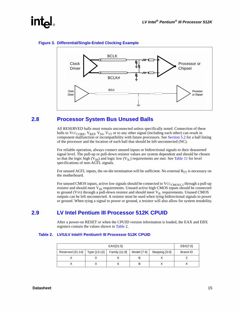
2.7 Processor System Bus Clock and Processor ClockingThe LV Intel Pentium III processor 512K has an auto-detect mechanism that allows the processor to use either single-ended or differential signaling for the system bus and processor clocking. The processor checks to see if the signal on ball AD1 is toggling. If this signal is toggling then the processor operates in differential mode. Refer to Figure 3 for an example on differential clocking. Resistor values and clock topology are listed in the appropriate platform design guide for a differential implementation.
Note: In this document, references to BCLK also apply to its complement signal (BCLK#) in differential implementations and when noted otherwise.
14 Datasheet
LV Intel® Pentium® III Processor 512K
2.8 Processor System Bus Unused BallsAll RESERVED balls must remain unconnected unless specifically noted. Connection of these balls to VCCCORE, VREF, VSS, VTT or to any other signal (including each other) can result in component malfunction or incompatibility with future processors. See Section 5.2 for a ball listing of the processor and the location of each ball that should be left unconnected (NC).
For reliable operation, always connect unused inputs or bidirectional signals to their deasserted signal level. The pull-up or pull-down resistor values are system dependent and should be chosen so that the logic high (VIH) and logic low (VIL) requirements are met. See Table 11 for level specifications of non-AGTL signals.
For unused AGTL inputs, the on-die termination will be sufficient. No external RTT is necessary on the motherboard.
For unused CMOS inputs, active low signals should be connected to VCCCMOS1.5 through a pull-up resistor and should meet VIH requirements. Unused active high CMOS inputs should be connected to ground (VSS) through a pull-down resistor and should meet VIL requirements. Unused CMOS outputs can be left unconnected. A resistor must be used when tying bidirectional signals to power or ground. When tying a signal to power or ground, a resistor will also allow for system testability.
2.9 LV Intel Pentium III Processor 512K CPUIDAfter a power-on RESET or when the CPUID version information is loaded, the EAX and EBX registers contain the values shown in Table 2.
Table 2. LV/ULV Intel® Pentium® III Processor 512K CPUID
Figure 3. Differential/Single-Ended Clocking Example
BCLK
BCLK#
ClockDriver
Processor orChipset
ClockDriver
BCLK Processoror Chipset
EAX[31:0] EBX[7:0]
Reserved [31:14] Type [13:12] Family [11:8] Model [7:4] Stepping [3:0] Brand ID
X 0 6 B X 2
X 0 6 B X 4
Datasheet 15
LV Intel® Pentium® III Processor 512K
3.0 Electrical Specifications
3.1 Processor System Bus Signal Groups
To simplify the following discussion, the processor system bus signals have been combined into groups by buffer type. All P6 family processor system bus outputs are open drain and require termination resistors. However, the LV Intel Pentium III processor 512K includes on-die termination for AGTL signals. This makes it unnecessary to place termination resistors on the platform, except in the case of the RESET# signal, which still requires external termination.
AGTL input signals have differential input buffers that use VREF as a reference signal. AGTL output signals require termination to 1.25 V. In this document, the term “AGTL Input” refers to the AGTL input group and to the AGTL I/O group when this group is receiving signals. Similarly, “AGTL Output” refers to the AGTL output group and to the AGTL I/O group when this group is driving signals.
The PWRGOOD signal input is a 1.8 V signal level and must be pulled up to VCCCMOS1.8. The VTT_PWRGD is not 1.8 V tolerant and must be connected to VTT (1.25 V). Other CMOS inputs (A20M#, IGNNE#, INIT#, LINT0/INTR, LINT1/NMI, PREQ#, SMI#, SLP#, and STPCLK#) are only 1.5 V tolerant and must be pulled up to VCCCMOS1.5. The CMOS, APIC, and TAP outputs are open drain and must be pulled to the appropriate level to meet the input specifications of the interfacing device.
The groups and the signals contained within each group are shown in Table 3. Refer to “Processor Interface” on page 59 for a description of these signals.
Table 3. System Bus Signal Groups (Sheet 1 of 2)
Group Name Signals
AGTL Input BPRI#, DEFER#, RESET#, RSP#, BR1#
AGTL Output PRDY#
AGTL I/OA[35:3]#, ADS#, AERR#, AP[1:0]#, BERR#, BINIT#, BNR#, BP[3:2]#, BPM[1:0]#, BR0#, D[63:0]#, DBSY#, DEP[7:0]#, DRDY#, HIT#, HITM#, LOCK#, REQ[4:0]#, RP#, RS[2:0]#, TRDY#
1.5 V CMOS Input A20M#, FLUSH#, IGNNE#, INIT#, LINT0/INTR, LINT1/NMI, PREQ#, SLP#, SMI#, STPCLK#
1.8 V CMOS Input PWRGOOD
1.5 V Open Drain Output FERR#, IERR#, THERMTRIP#
3.3 V Open Drain Output BSEL[1:0], VID[3:0, 25mV]
1.25 V input VTT_PWRGD
Clock BCLK, BCLK# (Differential Mode)
2.5 V Clock Input BCLK (Single Ended Mode)
NOTES:1. VCCCORE is the power supply for the core logic. 2. PLL1 and PLL2 are power/ground for the PLL analog section. See “Voltage Planes” on page 21 for
details.3. VTT is the power supply for the system bus buffers.4. VREF is the voltage reference for the AGTL input buffers.5. VSS is system ground.
16 Datasheet
LV Intel® Pentium® III Processor 512K
3.1.1 Asynchronous vs. Synchronous for System Bus Signals
All AGTL signals are synchronous to BCLK (BCLK/BCLK#). All of the CMOS, Clock, APIC, and TAP signals can be applied asynchronously to BCLK (BCLK/BCLK#). All APIC signals are synchronous to PICCLK. All TAP signals are synchronous to TCK.
3.1.2 System Bus Frequency Select Signals
The BSEL[1:0] (Select Processor System Bus Speed) signals are used to configure the processor for the system bus frequency. The VTT_PWRGD signal informs the processor to output the BSEL signals. During power up the BSEL signals are indeterminate for a small period of time. If the clock generator supports this dynamic BSEL selection, it should not sample the BSEL signals until the VTT_PWRGD signal is asserted. The assertion of the VTT_PWRGD signal indicates that the BSEL signals are stable and driven to a final state by the processor.
Table 4 shows the encoding scheme for BSEL[1:0]. The only supported system bus frequency for the LV Pentium III processor 512K is 133 MHz. If another frequency is used, the processor is not guaranteed to function properly.
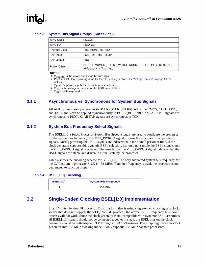
3.2 Single-Ended Clocking BSEL[1:0] Implementation
In an LV Intel Pentium III processor 512K platform that is using single-ended clocking or a clock source that does not support the VTT_PWRGD protocol, the normal BSEL frequency selection process will not work. Since the clock generator is not compatible with dynamic BSEL assertions, all BSEL[1:0] signals should not be connected together. Instead, the BSEL pins on the clock generator should be pulled-up to 3.3 V through a 1 KΩ, 5% resistor. This strapping forces the clock generator into 133 MHz clocking mode. It only supports 133 MHz capable processors.
APIC Clock PICCLK
APIC I/O PICD[1:0]
Thermal Diode THERMDN, THERMDP
TAP Input TCK, TDI, TMS, TRST#
TAP Output TDO
Power/Other CLKREF, VCMOS_REF, SLEWCTRL, NCHCTRL, PLL1, PLL2, RTTCTRL, VccCORE, VTT, VREF, VSS
Table 3. System Bus Signal Groups (Sheet 2 of 2)
NOTES:1. VCCCORE is the power supply for the core logic. 2. PLL1 and PLL2 are power/ground for the PLL analog section. See “Voltage Planes” on page 21 for
details.3. VTT is the power supply for the system bus buffers.4. VREF is the voltage reference for the AGTL input buffers.5. VSS is system ground.
Table 4. BSEL[1:0] Encoding
BSEL[1:0] System Bus Frequency
11 133 MHz
Datasheet 17
LV Intel® Pentium® III Processor 512K
3.3 Differential Host Bus Clocking Routing
LV Intel Pentium III processor 512K dual-processor platforms support differential host bus clock drivers. When operating in differential clocking mode, the BCLK and BCLK#/CLKREF form a differential pair of clock inputs. The differential pair of traces should be routed with special care and using standard differential signaling techniques. Refer to the LV Intel® Pentium® III Processor 512K Dual Processor Platform Design Guide for more information.
The following sections contain the recommended topology and routing for differential clocking in the LV Intel Pentium III processor 512K dual-processor platforms.
3.3.1 Differential Clocking BSEL[1:0] Implementation
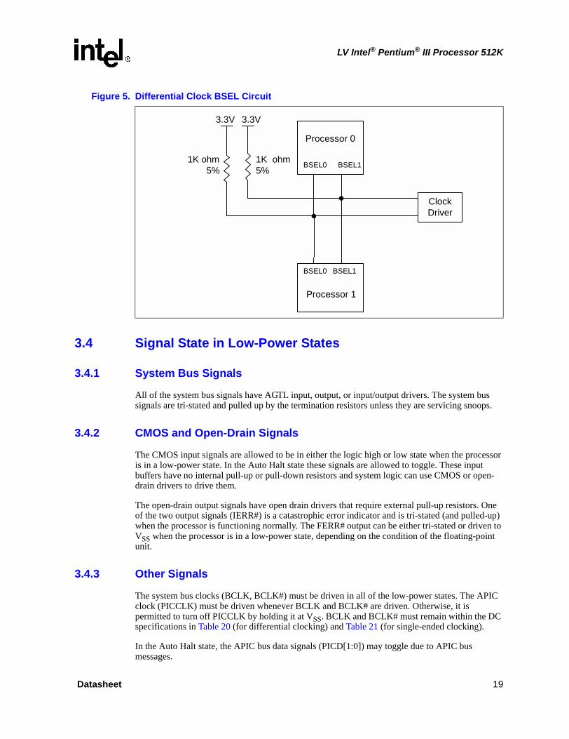
The System Bus Frequency Select Signals (BSEL[1:0]) are used to select the system bus frequency for the host bus agents. Frequency selection is determined by the processor(s) and driven out to the host bus clock generator. All system bus agents must operate at the same 133 MHz frequency. The BSEL balls for the processor are open drain signals and rely on a 3.3 V pull-up resistor to set the signal to a logic high level. Figure 5 shows the recommended implementation for a differentially clocked system.
Figure 4. Single Ended Clock BSEL Circuit (133 MHz)
NC NC NC NC
Processor 1 Processor 0 Clock Driver
BSEL0 BSEL1 BSEL0 BSEL1 BSEL0 BSEL1
3.3V 3.3V
1 KΩ
5%
1 KΩ
5%
18 Datasheet
LV Intel® Pentium® III Processor 512K
3.4 Signal State in Low-Power States
3.4.1 System Bus Signals
All of the system bus signals have AGTL input, output, or input/output drivers. The system bus signals are tri-stated and pulled up by the termination resistors unless they are servicing snoops.
3.4.2 CMOS and Open-Drain Signals
The CMOS input signals are allowed to be in either the logic high or low state when the processor is in a low-power state. In the Auto Halt state these signals are allowed to toggle. These input buffers have no internal pull-up or pull-down resistors and system logic can use CMOS or open-drain drivers to drive them.
The open-drain output signals have open drain drivers that require external pull-up resistors. One of the two output signals (IERR#) is a catastrophic error indicator and is tri-stated (and pulled-up) when the processor is functioning normally. The FERR# output can be either tri-stated or driven to VSS when the processor is in a low-power state, depending on the condition of the floating-point unit.
3.4.3 Other Signals
The system bus clocks (BCLK, BCLK#) must be driven in all of the low-power states. The APIC clock (PICCLK) must be driven whenever BCLK and BCLK# are driven. Otherwise, it is permitted to turn off PICCLK by holding it at VSS. BCLK and BCLK# must remain within the DC specifications in Table 20 (for differential clocking) and Table 21 (for single-ended clocking).
In the Auto Halt state, the APIC bus data signals (PICD[1:0]) may toggle due to APIC bus messages.
Figure 5. Differential Clock BSEL Circuit
Processor 0
BSEL0
BSEL1
ClockDriver
1K ohm5%
1K ohm5%
3.3V 3.3V
Processor 1
BSEL0
BSEL1
Datasheet 19
LV Intel® Pentium® III Processor 512K
3.5 Test Access Port (TAP) Connection
The TAP interface is an implementation of the IEEE 1149.1 (“JTAG”) standard. Due to the voltage levels supported by the TAP interface, Intel recommends that the LV Intel Pentium III processor 512K and the other 1.5 V JTAG specification compliant devices be placed last in the JTAG chain, behind any system devices with 3.3 V or 5.0 V JTAG interfaces. A translation buffer should be used to reduce the TDO output voltage of the last 3.3/5.0 V device down to the 1.5 V range that the processor can tolerate. Multiple copies of TMS and TRST# must be provided, one for each voltage level.
A Debug Port and connector may be placed at the start and at the end of the JTAG chain that contains the processor, with TDI to the first component coming from the Debug Port, and TDO from the last component going to the Debug Port. There are no requirements for placing the processor in the JTAG chain, except for those that are dictated by the voltage requirements of the TAP signals.
3.6 Power Supply Requirements
3.6.1 Decoupling Guidelines
Due to the large number of transistors and high internal clock speeds, the processor is capable of generating large average current swings between low and full power states. These fluctuations can cause voltages on power planes to sag below their nominal values if bulk decoupling is not adequate. Care must be taken in the board design to ensure that the voltage provided to the processor remains within the specifications listed in Table 7. Failure to do so can result in timing violations (in the event of a voltage sag) or a reduced lifetime of the component (in the event of a voltage overshoot).
3.6.2 Processor VCCCORE Decoupling
The regulator for the VCCCORE input must be capable of delivering the dICCCORE/dt (defined in Table 7) while maintaining the required tolerances (defined in Table 9). Failure to meet these specifications can result in timing violations (during VCCCORE sag) or a reduced lifetime of the component (during VCCCORE overshoot).
The processor requires both high frequency and bulk decoupling on the system motherboard for proper AGTL bus operation. The minimum recommendation for the processor decoupling requirement is listed below.
The LV Intel Pentium III processor 512K has eight 0.68-µF surface mount decoupling capacitors. Six 0.68-µF capacitors are on VCCCORE and two 0.68-µF capacitors are on VTT. In addition to the package capacitors, sufficient board level capacitors are also necessary for power supply decoupling. These guidelines are as follows:
• High and Mid Frequency VCCCORE decoupling – Place twenty-four 0.22-µF 0603 capacitors directly under the package on the solder side of the motherboard, using at least two vias per capacitor node. Ten 10-µF X7R 6.3 V 1206-size ceramic capacitors should be placed around the package periphery near the balls. Trace lengths to the vias should be designed to minimize inductance. Avoid bending traces to minimize ESL.
• High and Mid Frequency VTT decoupling – Place ten 1-µF X7R 0603 ceramic capacitors close to the package. Via and trace guidelines are the same as above.
20 Datasheet
LV Intel® Pentium® III Processor 512K
For additional decoupling requirements, please refer to the appropriate platform design guide for recommended capacitor component value/quantity and placement.
3.6.3 Voltage Planes
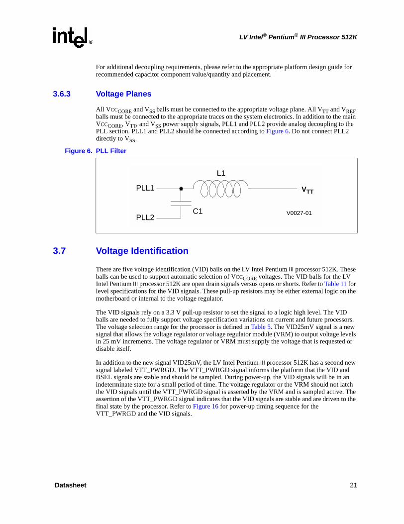
All VCCCORE and VSS balls must be connected to the appropriate voltage plane. All VTT and VREF balls must be connected to the appropriate traces on the system electronics. In addition to the main VCCCORE, VTT, and VSS power supply signals, PLL1 and PLL2 provide analog decoupling to the PLL section. PLL1 and PLL2 should be connected according to Figure 6. Do not connect PLL2 directly to VSS.
3.7 Voltage Identification
There are five voltage identification (VID) balls on the LV Intel Pentium III processor 512K. These balls can be used to support automatic selection of VCCCORE voltages. The VID balls for the LV Intel Pentium III processor 512K are open drain signals versus opens or shorts. Refer to Table 11 for level specifications for the VID signals. These pull-up resistors may be either external logic on the motherboard or internal to the voltage regulator.
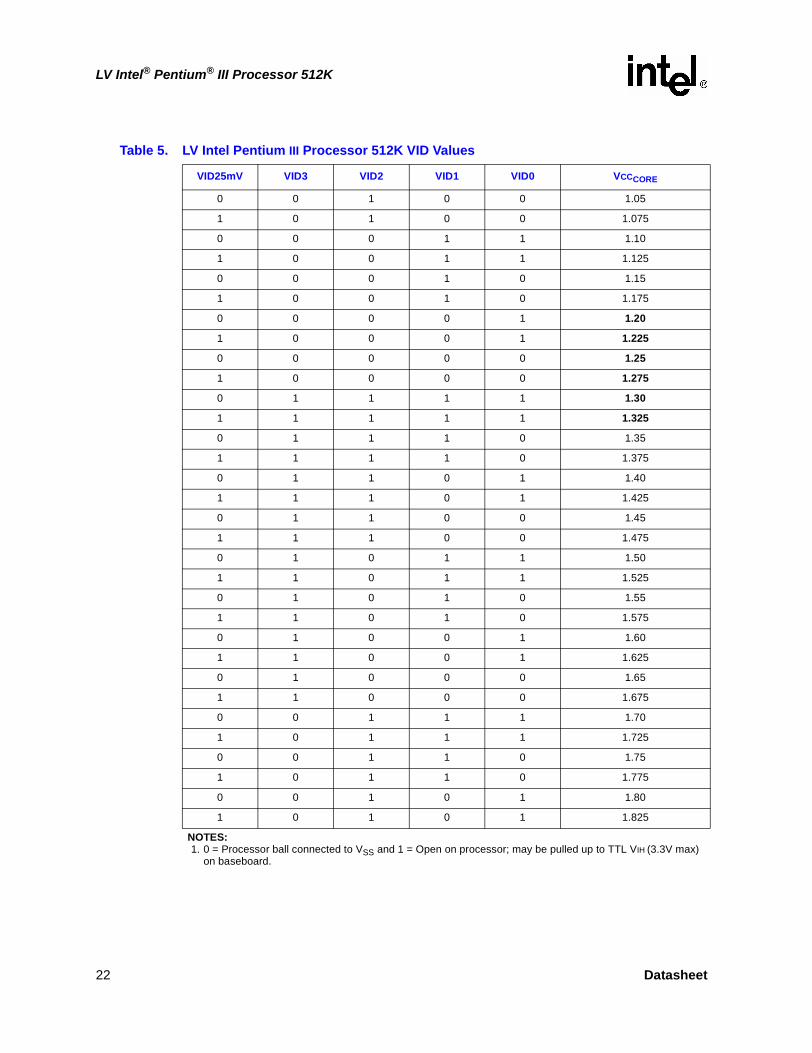
The VID signals rely on a 3.3 V pull-up resistor to set the signal to a logic high level. The VID balls are needed to fully support voltage specification variations on current and future processors. The voltage selection range for the processor is defined in Table 5. The VID25mV signal is a new signal that allows the voltage regulator or voltage regulator module (VRM) to output voltage levels in 25 mV increments. The voltage regulator or VRM must supply the voltage that is requested or disable itself.
In addition to the new signal VID25mV, the LV Intel Pentium III processor 512K has a second new signal labeled VTT_PWRGD. The VTT_PWRGD signal informs the platform that the VID and BSEL signals are stable and should be sampled. During power-up, the VID signals will be in an indeterminate state for a small period of time. The voltage regulator or the VRM should not latch the VID signals until the VTT_PWRGD signal is asserted by the VRM and is sampled active. The assertion of the VTT_PWRGD signal indicates that the VID signals are stable and are driven to the final state by the processor. Refer to Figure 16 for power-up timing sequence for the VTT_PWRGD and the VID signals.
Figure 6. PLL Filter
PLL1
PLL2
VCCT
V0027-01
L1
C1
R1VTT
Datasheet 21
LV Intel® Pentium® III Processor 512K
Table 5. LV Intel Pentium III Processor 512K VID Values
VID25mV VID3 VID2 VID1 VID0 VCCCORE
0 0 1 0 0 1.05
1 0 1 0 0 1.075
0 0 0 1 1 1.10
1 0 0 1 1 1.125
0 0 0 1 0 1.15
1 0 0 1 0 1.175
0 0 0 0 1 1.20
1 0 0 0 1 1.225
0 0 0 0 0 1.25
1 0 0 0 0 1.275
0 1 1 1 1 1.30
1 1 1 1 1 1.325
0 1 1 1 0 1.35
1 1 1 1 0 1.375
0 1 1 0 1 1.40
1 1 1 0 1 1.425
0 1 1 0 0 1.45
1 1 1 0 0 1.475
0 1 0 1 1 1.50
1 1 0 1 1 1.525
0 1 0 1 0 1.55
1 1 0 1 0 1.575
0 1 0 0 1 1.60
1 1 0 0 1 1.625
0 1 0 0 0 1.65
1 1 0 0 0 1.675
0 0 1 1 1 1.70
1 0 1 1 1 1.725
0 0 1 1 0 1.75
1 0 1 1 0 1.775
0 0 1 0 1 1.80
1 0 1 0 1 1.825
NOTES:1. 0 = Processor ball connected to VSS and 1 = Open on processor; may be pulled up to TTL VIH (3.3V max)
on baseboard.
22 Datasheet
LV Intel® Pentium® III Processor 512K
The VID balls should be pulled up to a 3.3-V level. This may be accomplished with pull-ups internal to the voltage regulator, which ensures valid VID pull-up voltage during power-up and power-down sequences. When external resistors are used for the VID[3:0, 25mV] signal, the power source must be guaranteed to be stable whenever the supply to the voltage regulator is stable. This will prevent the possibility of the processor supply going above the specified VCCCORE in the event of a failure in the supply for the VID lines. In the case of a DC-to-DC converter, this can be accomplished by using the input voltage to the converter for the VID line pull-ups. A resistor equal to 1 KΩ may be used to connect the VID signals to the voltage regulator input.
Important: Intel requires that designs utilize VRM 8.5 and not IMVP-II specifications to meet the LV Intel Pentium III processor 512K requirements.
To re-emphasize, VRM 8.5 introduces two new signals [VID25mV and VTT_PWRGD] that are used by the LV Intel Pentium III processor 512K and platform. Failing to connect these two new balls as documented in the design guidelines (provided in the LV Intel® Pentium® III Processor 512K Dual Processor Platform Design Guide) will prevent the LV Intel Pentium III processor 512K from operating at the specified voltage levels and core frequency. Figure 7 provides a high-level interconnection schematic. Please refer to the VRM 8.5 DC-DC Converter Design Guideline and the appropriate platform design guidelines for further detailed information on the voltage identification and bus select implementation.
Refer to Figure 16 for VID power-up sequence and timing requirements.
Note: Please refer to the LV Intel® Pentium® III Processor 512K Dual Processor Platform Design Guide for VTT_PWRGD implementation for an LV Intel Pentium III processor 512K platform.
Separate VRM 8.5 voltage regulators and processor core voltage planes are required for each processor in a dual-processor system.
Figure 7. VTT Power Good and Bus Select Interconnect Diagram
VRM 8.5Voltage Regulator
Processor
ClockDriver
Vtt
VTT_PWRGD(output)
VTT_PWRGD(input)
Vtt
R
Vtt
VID[3:0,25mV]
Vcc_core Vcc_core
BSEL [1:0]
Datasheet 23
LV Intel® Pentium® III Processor 512K
3.8 System Bus Clock and Processor Clocking
The BCLK and BCLK# clock inputs directly control the operating speed of the system bus interface. All system bus timing parameters are specified with respect to the crossing point of the rising edge of the BCLK input and the falling edge of the BCLK# input. The LV Intel Pentium III processor 512K core frequency is a multiple of the BCLK frequency. The processor core frequency is configured during manufacturing. The configured bus ratio is visible to software in the power-on configuration register.
Multiplying the bus clock frequency is necessary to increase performance while allowing for easier distribution of signals within the system. Clock multiplication within the processor is provided by the internal Phase Lock Loop (PLL), which requires constant frequency BCLK, BCLK# inputs. During Reset, the PLL requires some amount of time to acquire the phase of BCLK and BCLK#. This time is called the PLL lock latency, which is specified in Table 17 on page 33; see the AC timing parameter for T18.
3.9 Maximum Ratings
Table 6 contains the LV Intel Pentium III processor 512K stress ratings. Functional operation at the absolute maximum and minimum is neither implied nor guaranteed. The processor should not receive a clock while subjected to these conditions. Functional operating conditions are provided in the AC and DC tables. Extended exposure to the maximum ratings may affect device reliability. Furthermore, although the processor contains protective circuitry to resist damage from static electric discharge, one should always take precautions to avoid high static voltages or electric fields.
Table 6. LV Intel Pentium III Processor 512K Absolute Maximum Ratings
Symbol Parameter Min Max Unit Notes
TStorage Storage Temperature –40 85 °C 1
VCCCORE(Abs) Supply Voltage with respect to VSS –0.5 1.75 V
VTT System Bus Buffer Voltage with respect to VSS –0.3 1.75 V
VIN AGTL System Bus Buffer DC Input Voltage with respect to VSS –0.3 1.75 V 2, 3
VIN125 1.25 V Buffer DC Input Voltage with respect to VSS –0.3 1.75 V 4
VIN15 1.5 V Buffer DC Input Voltage with respect to VSS –0.3 2.0 V 5
VIN18 1.8 V Buffer DC Input Voltage with respect to VSS –0.3 2.0 V 6
VIN20 2.0 V Buffer DC Input Voltage with respect to VSS –0.3 2.4 V 7
VIN25 2.5 V Buffer DC Input Voltage with respect to VSS –0.3 3.3 V 8
VINVID VID ball DC Input Voltage with respect to VSS — 3.465 V 9
IVID VID Current -0.3 3.6 mA 9
NOTES:1. The shipping container is only rated for 65° C.2. Parameter applies to the AGTL signal groups only. Compliance with both VIN AGTL specifications is
required.3. The voltage on the AGTL signals must never be below –0.3 or above 1.75 V with respect to ground.4. Parameter applies to CLKREF, TESTHI, VTT_PWRGD signals.5. Parameter applies to CMOS, Open-drain, APIC, TESTLO and TAP bus signal groups only.6. Parameter applies to PWRGOOD signal.7. Parameter applies to PICCLK signal.8. Parameter applies to BCLK signal in Single-Ended Clocking Mode.9. Parameter applies to each VID ball individually.
24 Datasheet
LV Intel® Pentium® III Processor 512K
3.10 DC Specifications
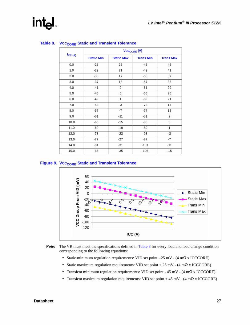
Tables 7 through 11 list the DC specifications for the LV Intel Pentium III processor 512K. Specifications are valid only while meeting specifications for the junction temperature, clock frequency, and input voltages. The junction temperature range for all DC specifications is 0° C to 100° C. Care should be taken to read all notes associated with each parameter. The VCCCORE tolerances for the LV Intel Pentium III processor 512K are not specified as a percentage of nominal. The tolerances are instead specified in the form of load lines for the static and transient cases in Table 9. An illustration of the load lines is shown in Figure 9.
Table 7. Power Specifications for LV Intel Pentium III Processor 512K
Symbol Parameter Frequency(MHz)
Processor Signature Min Typ Max Unit Tolerance
VCCCORETransient VCCCORE for core logic 1.15 V
VCCCORE,DC Static VCCCORE for core logic 1.15 V
VCCCMOS1.5 1.5 V CMOS voltage 1.5 V ± 10%
VCCCMOS1.8 1.8 V CMOS voltage 1.8 V ± 10%
VCCCMOS3.3 3.3 V CMOS voltage 3.3 V ± 10%
VTTVCC for System Bus Buffers, Transient tolerance 1.13 1.25 1.36 V ± 9%
VTT,DCVCC for System Bus Buffers, Static tolerance 1.21 1.25 1.28 V ±3%
IccCORE
Current for VCCCORE at core frequency
1000933800
06B206B4
10.9410.59.57
A
ITT Current for VTT 2.3 A
ICCCMOS1.5 ICC for VCCCMOS1.5 250 mA
ICCCMOS1.8 ICC for VCCCMOS1.8 1 mA
ICCCMOS3.3 ICC for VCCCMOS3.3 35 mA
IccCORE,SGProcessor Stop Grant current1.15 V 4.68 A
ILVID VID leakage current 0.5 mA
Datasheet 25
LV Intel® Pentium® III Processor 512K
Figure 8. Power Supply Current Slew Rate (dICCCORE/dt)
Slew Rate – 26A Load Step Slew Rate (26A) – ICC @ socket
0
5
10
15
20
25
30
0 1 2 3 4 5 6
Icc
@ s
ocke
t (A
)
PW L Slew Rate Data Tim e (uS) Icc @ socket (A)
0.1 26.230.15 23.18
0.5 20.031 21.10
1.5 21.882 22.29
2.5 22.303 22.07
3.5 21.784 21.58
4.5 21.51
Time (s)
26 Datasheet
LV Intel® Pentium® III Processor 512K
Note: The VR must meet the specifications defined in Table 8 for every load and load change condition corresponding to the following equations:
• Static minimum regulation requirements: VID set point - 25 mV - (4 mΩ x ICCCORE)
• Static maximum regulation requirements: VID set point + 25 mV - (4 mΩ x ICCCORE)
• Transient minimum regulation requirements: VID set point - 45 mV - (4 mΩ x ICCCORE)
• Transient maximum regulation requirements: VID set point + 45 mV - (4 mΩ x ICCCORE)
Table 8. VCCCORE Static and Transient Tolerance
ICC (A)VCCCORE (V)
Static Min Static Max Trans Min Trans Max
0.0 -25 25 -45 45
1.0 -29 21 -49 41
2.0 -33 17 -53 37
3.0 -37 13 -57 33
4.0 -41 9 -61 29
5.0 -45 5 -65 25
6.0 -49 1 -69 21
7.0 -53 -3 -73 17
8.0 -57 -7 -77 13
9.0 -61 -11 -81 9
10.0 -65 -15 -85 5
11.0 -69 -19 -89 1
12.0 -73 -23 -93 -3
13.0 -77 -27 -97 -7
14.0 -81 -31 -101 -11
15.0 -85 -35 -105 -15
Figure 9. VCCCORE Static and Transient Tolerance
-120-100-80-60-40-20
0204060
0.0 2.0 4.0 6.0 8.0 10.0
12.0
14.0
ICC (A)
VCC
Dro
op F
rom
VID
(mV)
Static MinStatic MaxTrans MinTrans Max
Datasheet 27
LV Intel® Pentium® III Processor 512K
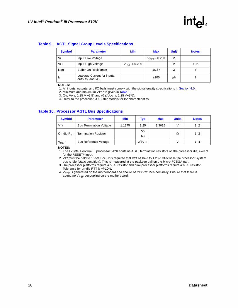
Table 9. AGTL Signal Group Levels Specifications
Symbol Parameter Min Max Unit Notes
VIL Input Low Voltage VREF - 0.200 V
VIH Input High Voltage VREF + 0.200 V 1, 2
Ron Buffer On Resistance 16.67 Ω 4
IL Leakage Current for inputs, outputs, and I/O ±100 µA 3
NOTES:1. All inputs, outputs, and I/O balls must comply with the signal quality specifications in Section 4.0.2. Minimum and maximum VTT are given in Table 10.3. (0 ≤ VIN ≤ 1.25 V +3%) and (0 ≤ VOUT ≤ 1.25 V+3%).4. Refer to the processor I/O Buffer Models for I/V characteristics.
Table 10. Processor AGTL Bus Specifications
Symbol Parameter Min Typ Max Units Notes
VTT Bus Termination Voltage 1.1375 1.25 1.3625 V 1, 2
On-die RTT Termination Resistor5668
Ω 1, 3
VREF Bus Reference Voltage 2/3VTT V 1, 4
NOTES:1. The LV Intel Pentium III processor 512K contains AGTL termination resistors on the processor die, except
for the RESET# input.2. VTT must be held to 1.25V ±9%. It is required that VTT be held to 1.25V ±3% while the processor system
bus is idle (static condition). This is measured at the package ball on the Micro-FCBGA part.3. Uni-processor platforms require a 56 Ω resistor and dual-processor platforms require a 68 Ω resistor.
Tolerance for on-die RTT is +/-10%.4. VREF is generated on the motherboard and should be 2/3 VTT ±5% nominally. Ensure that there is
adequate VREF decoupling on the motherboard.
28 Datasheet
LV Intel® Pentium® III Processor 512K
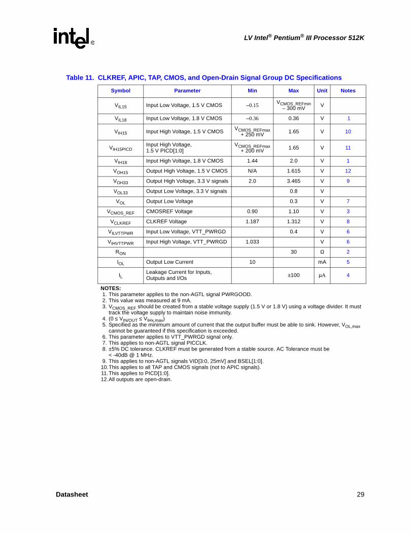
Table 11. CLKREF, APIC, TAP, CMOS, and Open-Drain Signal Group DC Specifications
Symbol Parameter Min Max Unit Notes
VIL15 Input Low Voltage, 1.5 V CMOS –0.15 VCMOS_REFmin – 300 mV V
VIL18 Input Low Voltage, 1.8 V CMOS –0.36 0.36 V 1
VIH15 Input High Voltage, 1.5 V CMOS VCMOS_REFmax + 250 mV 1.65 V 10
VIH15PICDInput High Voltage, 1.5 V PICD[1:0]
VCMOS_REFmax + 200 mV 1.65 V 11
VIH18 Input High Voltage, 1.8 V CMOS 1.44 2.0 V 1
VOH15 Output High Voltage, 1.5 V CMOS N/A 1.615 V 12
VOH33 Output High Voltage, 3.3 V signals 2.0 3.465 V 9
VOL33 Output Low Voltage, 3.3 V signals 0.8 V
VOL Output Low Voltage 0.3 V 7
VCMOS_REF CMOSREF Voltage 0.90 1.10 V 3
VCLKREF CLKREF Voltage 1.187 1.312 V 8
VILVTTPWR Input Low Voltage, VTT_PWRGD 0.4 V 6
VIHVTTPWR Input High Voltage, VTT_PWRGD 1.033 V 6
RON 30 Ω 2
IOL Output Low Current 10 mA 5
ILLeakage Current for Inputs, Outputs and I/Os ±100 µA 4
NOTES:1. This parameter applies to the non-AGTL signal PWRGOOD.2. This value was measured at 9 mA.3. VCMOS_REF should be created from a stable voltage supply (1.5 V or 1.8 V) using a voltage divider. It must
track the voltage supply to maintain noise immunity.4. (0 ≤ VIN/OUT ≤ VIHx,max)5. Specified as the minimum amount of current that the output buffer must be able to sink. However, VOL,max
cannot be guaranteed if this specification is exceeded.6. This parameter applies to VTT_PWRGD signal only.7. This applies to non-AGTL signal PICCLK.8. ±5% DC tolerance. CLKREF must be generated from a stable source. AC Tolerance must be
< -40dB @ 1 MHz.9. This applies to non-AGTL signals VID[3:0, 25mV] and BSEL[1:0].
10.This applies to all TAP and CMOS signals (not to APIC signals).11.This applies to PICD[1:0].12.All outputs are open-drain.
Datasheet 29

LV Intel® Pentium® III Processor 512K
3.11 AC Specifications
3.11.1 System Bus, Clock, APIC, TAP, CMOS, and Open-Drain AC Specifications
The processor system bus timings specified in this section are defined at the processor core (pads).
All system bus AC specifications for the AGTL signal group are relative to the crossing point of the rising edge of the BCLK input and falling edge of the BCLK# input. All AGTL timings are referenced to VREF for both “0” and “1” logic levels unless otherwise specified. All APIC, TAP, CMOS, and open-drain signals except PWRGOOD are referenced to 1.0 V. All minimum and maximum specifications are at points within the power supply ranges shown in Table 6 and junction temperatures (Tj) in the range 0° C to 100° C. Tj must be less than or equal to 100° C for all functional processor states.
Table 12. System Bus Clock AC Specifications (Differential)
Symbol Parameter Min Typ Max Unit Figure Notes1
System Bus Frequency 133 MHz
T1 BCLK Period - average 7.5 7.7 ns 12 2
T1abs BCLK Period – Instantaneous minimum 7.3 ns 2
T2 BCLK Cycle to Cycle Jitter 200 ps 2, 3, 4
T5 BCLK Rise Time 175 467 ps 12 2, 6
T6 BCLK Fall Time 175 467 ps 12 2, 6
Vcross for 1 V swing 0.51 0.76 V 11 7
Rise/Fall Time Matching 325 ps 5
BCLK Duty Cycle 45% 55% 2
NOTES:1. All AC timings for AGTL and CMOS signals are referenced to the BCLK and BCLK# crossing point. 2. Measured on differential waveform: defined as (BCLK - BCLK#).3. Not 100% tested. Specified by design/characterization.4. Due to the difficulty of accurately measuring clock jitter in a system, it is recommended that the clock driver be
designed to meet a period stability specification into a test load of 10 to 20 pF. This should be measured on therising edge of adjacent BCLKs at the BCLK and BCLK# crossing point. The jitter present must be accounted foras a component of BCLK skew between devices. Period difference is measured around 0 V crossing points.
5. Measurement taken from common mode waveform. Measure rise/fall time from 0.41 to 0.86 V. Rise/fall time matching is defined as “the instantaneous difference between maximum BCLK rise (fall) and minimum BCLK# fall (rise) time, or minimum BCLK rise (fall) and maximum BCLK# fall (rise) time”. This parameter is designed toguard waveform symmetry.
6. Rise time is measured from -0.35 V to 0.35 V and fall time is measured from 0.35 V to -0.35 V.7. Measured on common mode waveform - includes every rise/fall crossing.
30 Datasheet
LV Intel® Pentium® III Processor 512K
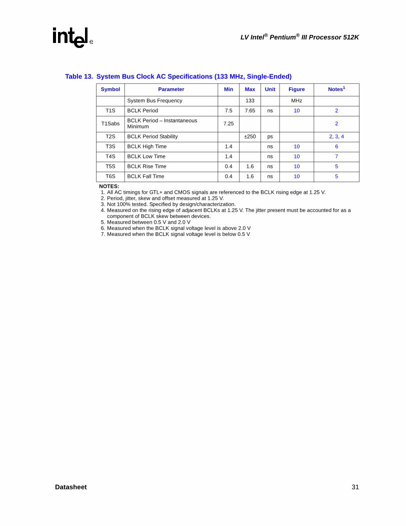
Table 13. System Bus Clock AC Specifications (133 MHz, Single-Ended)
Symbol Parameter Min Max Unit Figure Notes1
System Bus Frequency 133 MHz
T1S BCLK Period 7.5 7.65 ns 10 2
T1Sabs BCLK Period – Instantaneous Minimum 7.25 2
T2S BCLK Period Stability ±250 ps 2, 3, 4
T3S BCLK High Time 1.4 ns 10 6
T4S BCLK Low Time 1.4 ns 10 7
T5S BCLK Rise Time 0.4 1.6 ns 10 5
T6S BCLK Fall Time 0.4 1.6 ns 10 5
NOTES:1. All AC timings for GTL+ and CMOS signals are referenced to the BCLK rising edge at 1.25 V.2. Period, jitter, skew and offset measured at 1.25 V.3. Not 100% tested. Specified by design/characterization.4. Measured on the rising edge of adjacent BCLKs at 1.25 V. The jitter present must be accounted for as a
component of BCLK skew between devices.5. Measured between 0.5 V and 2.0 V6. Measured when the BCLK signal voltage level is above 2.0 V7. Measured when the BCLK signal voltage level is below 0.5 V
Datasheet 31
LV Intel® Pentium® III Processor 512K
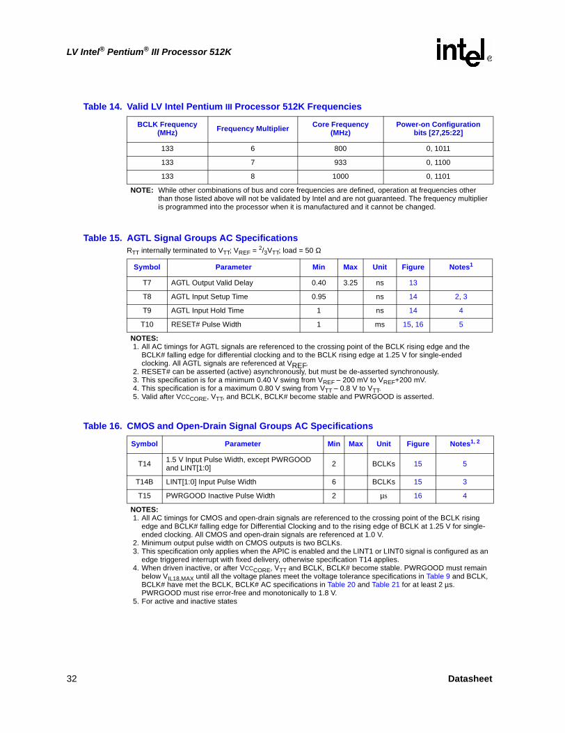
Table 14. Valid LV Intel Pentium III Processor 512K Frequencies
BCLK Frequency(MHz) Frequency Multiplier Core Frequency
(MHz)Power-on Configuration
bits [27,25:22]
133 6 800 0, 1011
133 7 933 0, 1100
133 8 1000 0, 1101
NOTE: While other combinations of bus and core frequencies are defined, operation at frequencies other than those listed above will not be validated by Intel and are not guaranteed. The frequency multiplier is programmed into the processor when it is manufactured and it cannot be changed.
Table 15. AGTL Signal Groups AC SpecificationsRTT internally terminated to VTT; VREF = 2/3VTT; load = 50 Ω
Symbol Parameter Min Max Unit Figure Notes1
T7 AGTL Output Valid Delay 0.40 3.25 ns 13
T8 AGTL Input Setup Time 0.95 ns 14 2, 3
T9 AGTL Input Hold Time 1 ns 14 4
T10 RESET# Pulse Width 1 ms 15, 16 5
NOTES:1. All AC timings for AGTL signals are referenced to the crossing point of the BCLK rising edge and the
BCLK# falling edge for differential clocking and to the BCLK rising edge at 1.25 V for single-ended clocking. All AGTL signals are referenced at VREF.
2. RESET# can be asserted (active) asynchronously, but must be de-asserted synchronously.3. This specification is for a minimum 0.40 V swing from VREF – 200 mV to VREF+200 mV.4. This specification is for a maximum 0.80 V swing from VTT – 0.8 V to VTT.5. Valid after VCCCORE, VTT, and BCLK, BCLK# become stable and PWRGOOD is asserted.
Table 16. CMOS and Open-Drain Signal Groups AC Specifications
Symbol Parameter Min Max Unit Figure Notes1, 2
T14 1.5 V Input Pulse Width, except PWRGOOD and LINT[1:0] 2 BCLKs 15 5
T14B LINT[1:0] Input Pulse Width 6 BCLKs 15 3
T15 PWRGOOD Inactive Pulse Width 2 µs 16 4
NOTES:1. All AC timings for CMOS and open-drain signals are referenced to the crossing point of the BCLK rising
edge and BCLK# falling edge for Differential Clocking and to the rising edge of BCLK at 1.25 V for single-ended clocking. All CMOS and open-drain signals are referenced at 1.0 V.
2. Minimum output pulse width on CMOS outputs is two BCLKs.3. This specification only applies when the APIC is enabled and the LINT1 or LINT0 signal is configured as an
edge triggered interrupt with fixed delivery, otherwise specification T14 applies.4. When driven inactive, or after VCCCORE, VTT and BCLK, BCLK# become stable. PWRGOOD must remain
below VIL18,MAX until all the voltage planes meet the voltage tolerance specifications in Table 9 and BCLK, BCLK# have met the BCLK, BCLK# AC specifications in Table 20 and Table 21 for at least 2 µs. PWRGOOD must rise error-free and monotonically to 1.8 V.
5. For active and inactive states
32 Datasheet
LV Intel® Pentium® III Processor 512K
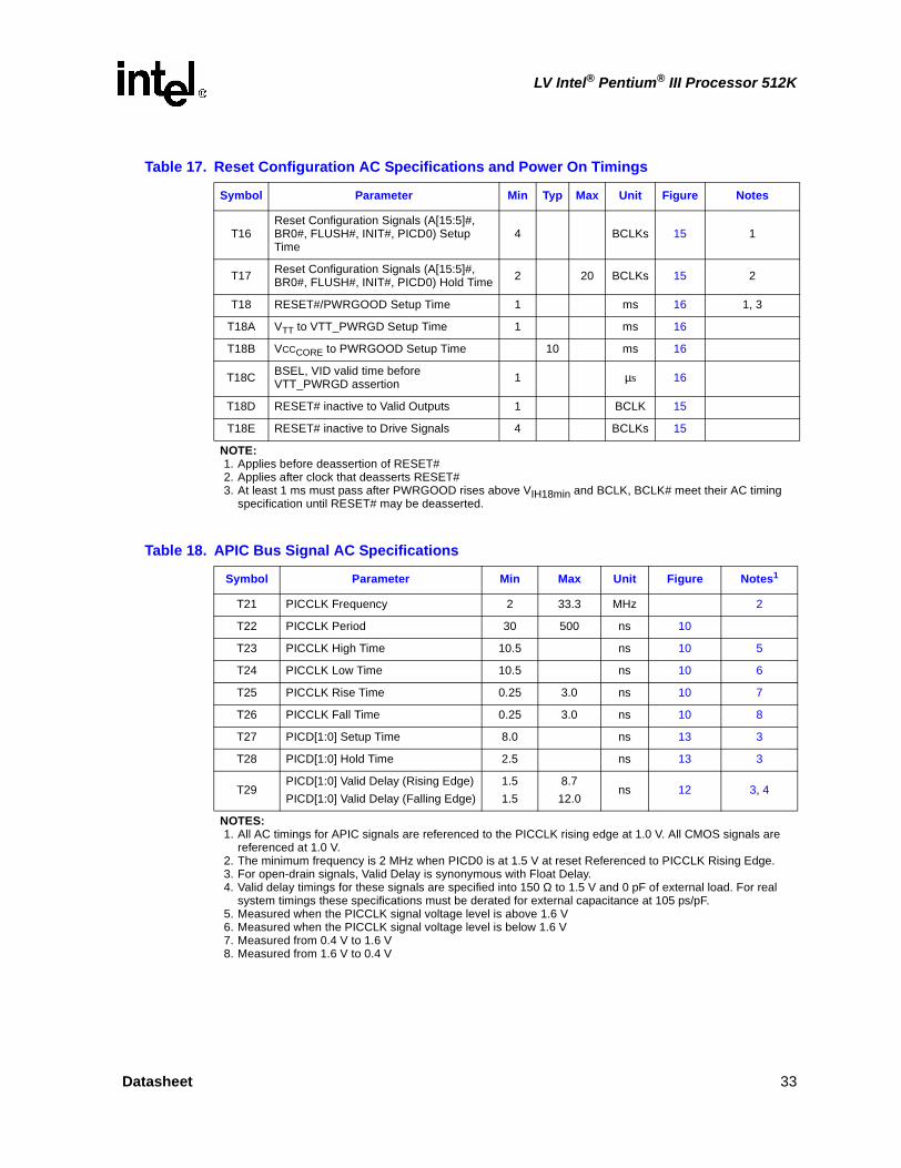
Table 17. Reset Configuration AC Specifications and Power On Timings
Symbol Parameter Min Typ Max Unit Figure Notes
T16Reset Configuration Signals (A[15:5]#, BR0#, FLUSH#, INIT#, PICD0) Setup Time
4 BCLKs 15 1
T17 Reset Configuration Signals (A[15:5]#, BR0#, FLUSH#, INIT#, PICD0) Hold Time 2 20 BCLKs 15 2
T18 RESET#/PWRGOOD Setup Time 1 ms 16 1, 3
T18A VTT to VTT_PWRGD Setup Time 1 ms 16
T18B VCCCORE to PWRGOOD Setup Time 10 ms 16
T18C BSEL, VID valid time before VTT_PWRGD assertion 1 µs 16
T18D RESET# inactive to Valid Outputs 1 BCLK 15
T18E RESET# inactive to Drive Signals 4 BCLKs 15
NOTE:1. Applies before deassertion of RESET#2. Applies after clock that deasserts RESET#3. At least 1 ms must pass after PWRGOOD rises above VIH18min and BCLK, BCLK# meet their AC timing
specification until RESET# may be deasserted.
Table 18. APIC Bus Signal AC Specifications
Symbol Parameter Min Max Unit Figure Notes1
T21 PICCLK Frequency 2 33.3 MHz 2
T22 PICCLK Period 30 500 ns 10
T23 PICCLK High Time 10.5 ns 10 5
T24 PICCLK Low Time 10.5 ns 10 6
T25 PICCLK Rise Time 0.25 3.0 ns 10 7
T26 PICCLK Fall Time 0.25 3.0 ns 10 8
T27 PICD[1:0] Setup Time 8.0 ns 13 3
T28 PICD[1:0] Hold Time 2.5 ns 13 3
T29PICD[1:0] Valid Delay (Rising Edge)PICD[1:0] Valid Delay (Falling Edge)
1.51.5
8.712.0
ns 12 3, 4
NOTES:1. All AC timings for APIC signals are referenced to the PICCLK rising edge at 1.0 V. All CMOS signals are
referenced at 1.0 V.2. The minimum frequency is 2 MHz when PICD0 is at 1.5 V at reset Referenced to PICCLK Rising Edge.3. For open-drain signals, Valid Delay is synonymous with Float Delay.4. Valid delay timings for these signals are specified into 150 Ω to 1.5 V and 0 pF of external load. For real
system timings these specifications must be derated for external capacitance at 105 ps/pF.5. Measured when the PICCLK signal voltage level is above 1.6 V6. Measured when the PICCLK signal voltage level is below 1.6 V7. Measured from 0.4 V to 1.6 V8. Measured from 1.6 V to 0.4 V
Datasheet 33
LV Intel® Pentium® III Processor 512K
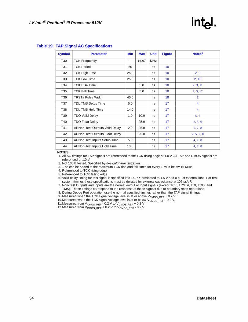
Table 19. TAP Signal AC Specifications
Symbol Parameter Min Max Unit Figure Notes1
T30 TCK Frequency — 16.67 MHz
T31 TCK Period 60 — ns 10
T32 TCK High Time 25.0 ns 10 2, 9
T33 TCK Low Time 25.0 ns 10 2, 10
T34 TCK Rise Time 5.0 ns 10 2, 3, 11
T35 TCK Fall Time 5.0 ns 10 2, 3, 12
T36 TRST# Pulse Width 40.0 ns 18 2
T37 TDI, TMS Setup Time 5.0 ns 17 4
T38 TDI, TMS Hold Time 14.0 ns 17 4
T39 TDO Valid Delay 1.0 10.0 ns 17 5, 6
T40 TDO Float Delay 25.0 ns 17 2, 5, 6
T41 All Non-Test Outputs Valid Delay 2.0 25.0 ns 17 5, 7, 8
T42 All Non-Test Outputs Float Delay 25.0 ns 17 2, 5, 7, 8
T43 All Non-Test Inputs Setup Time 5.0 ns 17 4, 7, 8
T44 All Non-Test Inputs Hold Time 13.0 ns 17 4, 7, 8
NOTES:1. All AC timings for TAP signals are referenced to the TCK rising edge at 1.0 V. All TAP and CMOS signals are
referenced at 1.0 V.2. Not 100% tested. Specified by design/characterization.3. 1 ns can be added to the maximum TCK rise and fall times for every 1 MHz below 16 MHz.4. Referenced to TCK rising edge5. Referenced to TCK falling edge6. Valid delay timing for this signal is specified into 150 Ω terminated to 1.5 V and 0 pF of external load. For real
system timings these specifications must be derated for external capacitance at 105 ps/pF.7. Non-Test Outputs and Inputs are the normal output or input signals (except TCK, TRST#, TDI, TDO, and
TMS). These timings correspond to the response of these signals due to boundary scan operations.8. During Debug Port operation use the normal specified timings rather than the TAP signal timings.9. Measured when the TCK signal voltage level is at or above VCMOS_REF + 0.2 V.10.Measured when the TCK signal voltage level is at or below VCMOS_REF - 0.2 V.11.Measured from VCMOS_REF - 0.2 V to VCMOS_REF + 0.2 V12.Measured from VCMOS_REF + 0.2 V to VCMOS_REF - 0.2 V
34 Datasheet
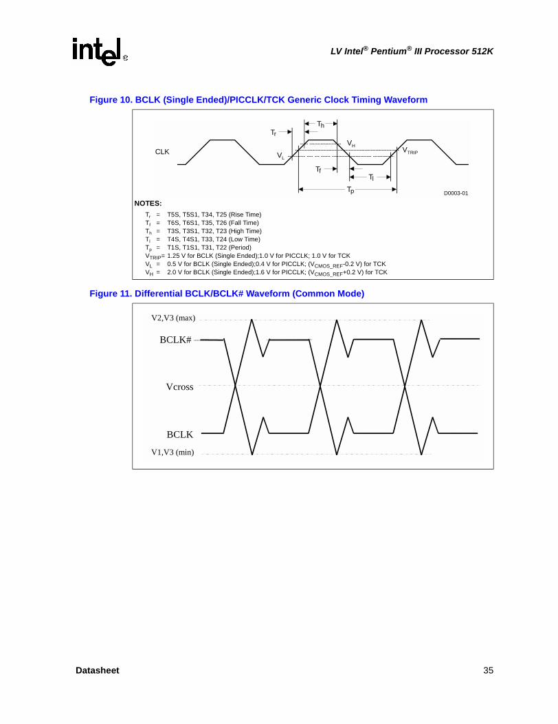
LV Intel® Pentium® III Processor 512K
Figure 10. BCLK (Single Ended)/PICCLK/TCK Generic Clock Timing Waveform
NOTES:Tr = T5S, T5S1, T34, T25 (Rise Time)Tf = T6S, T6S1, T35, T26 (Fall Time)Th = T3S, T3S1, T32, T23 (High Time)Tl = T4S, T4S1, T33, T24 (Low Time)Tp = T1S, T1S1, T31, T22 (Period) VTRIP= 1.25 V for BCLK (Single Ended);1.0 V for PICCLK; 1.0 V for TCKVL = 0.5 V for BCLK (Single Ended);0.4 V for PICCLK; (VCMOS_REF-0.2 V) for TCKVH = 2.0 V for BCLK (Single Ended);1.6 V for PICCLK; (VCMOS_REF+0.2 V) for TCK
Figure 11. Differential BCLK/BCLK# Waveform (Common Mode)
CLK VH
VLV TRIP
Th
Tl
Tp
Tr
Tf
D0003-01
BCLK
BCLK#
Vcross
V2,V3 (max)
V1,V3 (min)
Datasheet 35
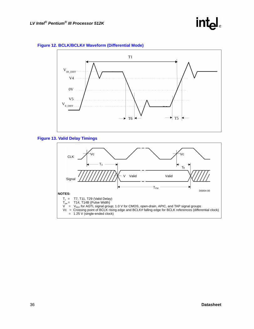
LV Intel® Pentium® III Processor 512K
Figure 12. BCLK/BCLK# Waveform (Differential Mode)
Figure 13. Valid Delay Timings
NOTES:Tx = T7, T11, T29 (Valid Delay)Tpw = T14, T14B (Pulse Width)V = VREF for AGTL signal group; 1.0 V for CMOS, open-drain, APIC, and TAP signal groupsVc = Crossing point of BCLK rising edge and BCLK# falling edge for BCLK references (differential clock)
= 1.25 V (single-ended clock)
0V
T6 T5
T1
V4
V5
VIH_DIFF
VIl_DIFF
CLK
Signal
TXT x
TPW
V Valid Valid
D0004-00
Vc Vc
36 Datasheet
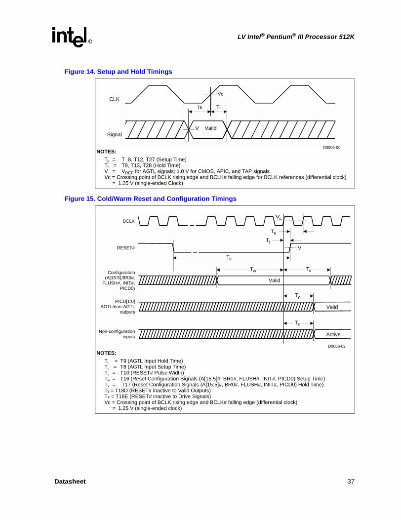
LV Intel® Pentium® III Processor 512K
Figure 14. Setup and Hold Timings
NOTES:Ts = T 8, T12, T27 (Setup Time)Th = T9, T13, T28 (Hold Time)V = VREF for AGTL signals; 1.0 V for CMOS, APIC, and TAP signalsVc = Crossing point of BCLK rising edge and BCLK# falling edge for BCLK references (differential clock)
= 1.25 V (single-ended Clock)
Figure 15. Cold/Warm Reset and Configuration Timings
NOTES:Tt = T9 (AGTL Input Hold Time)Tu = T8 (AGTL Input Setup Time)Tv = T10 (RESET# Pulse Width)Tw = T16 (Reset Configuration Signals (A[15:5]#, BR0#, FLUSH#, INIT#, PICD0) Setup Time)Tx = T17 (Reset Configuration Signals (A[15:5]#, BR0#, FLUSH#, INIT#, PICD0) Hold Time) Ty = T18D (RESET# inactive to Valid Outputs)Tz = T18E (RESET# inactive to Drive Signals)Vc = Crossing point of BCLK rising edge and BCLK# falling edge (differential clock)
= 1.25 V (single-ended clock)
CLK
Signal V Valid
ThTs
D0005-00
Vc
BCLK
RESET#
Tv
Tx
Tt
Tu
VC
V
D0006-02
Configuration(A[15:5], BREQ0#,
FLUSH#, INIT#,PICD0)
Tw
Valid
PICD[1:0]AGTL/non-AGTL
outputs
Non-configurationinputs
Ty
Valid
Tz
Active
(A[15:5],BR0#
Datasheet 37
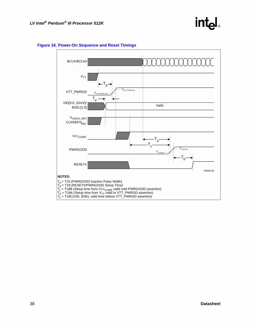
LV Intel® Pentium® III Processor 512K
Figure 16. Power-On Sequence and Reset Timings
NOTES:Ta = T15 (PWRGOOD Inactive Pulse Width)Tb = T18 (RESET#/PWRGOOD Setup Time)Tc = T18B (Setup time from VCCCORE valid until PWRGOOD assertion)Td = T18A (Setup time from VTT valid to VTT_PWRGD assertion)Te = T18C(VID, BSEL valid time before VTT_PWRGD assertion)
VCCT
Valid
VTTPWRGD
VID[4:0]/BSEL[1:0]
CMOSREF/CLKREF/VREF
PWRGOOD
RESET#
BCLK/BCLK#
VIH18,minVIL18,max
VIHVTTPWR,minVILVTTPWR,max
TaTc
Tb
VCC
V0040-00
Te
Td
VTT_PWRGD
VID[3:0, 25mV]/
VCMOS_REF
VTT
VCCCORE
38 Datasheet
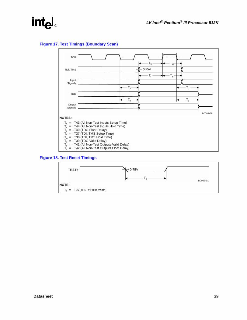
LV Intel® Pentium® III Processor 512K
Figure 17. Test Timings (Boundary Scan)
NOTES:Tr = T43 (All Non-Test Inputs Setup Time)Ts = T44 (All Non-Test Inputs Hold Time)Tu = T40 (TDO Float Delay)Tv = T37 (TDI, TMS Setup Time)Tw = T38 (TDI, TMS Hold Time)Tx = T39 (TDO Valid Delay)Ty = T41 (All Non-Test Outputs Valid Delay)Tz = T42 (All Non-Test Outputs Float Delay)
Figure 18. Test Reset Timings
NOTE:Tq = T36 (TRST# Pulse Width)
TCK
TDI, TMS
InputSignals
TDO
OutputSignals
0.75V
Tv Tw
Tr Ts
Tx Tu
Ty Tz
D0008-01
TRST# 0.75V
TqD0009-01
Datasheet 39
LV Intel® Pentium® III Processor 512K
4.0 System Signal Simulations
Systems must be simulated using the LV Intel Pentium III processor 512K IBIS Models to determine if they are compliant with this specification. All references to BCLK signal quality also apply to BCLK# for differential clocking.
4.1 System Bus Clock (BCLK) and PICCLK DCSpecifications and AC Signal Quality Specifications
Table 20. BCLK (Differential) DC Specifications and AC Signal Quality Specifications
Symbol Parameter Min Max Unit Figure Notes
V1 VIL,BCLK -0.2 0.35 V 11 1
V2 VIH,BCLK 0.92 1.45 V 11 1
V3 VIN Absolute Voltage Range -0.2 1.45 V 11 2, 4
V4 BCLK Rising Edge Ringback 0.35 V 12 3
V5 BCLK Falling Edge Ringback -0.35 V 12 3
NOTES:1. The clock must rise/fall monotonically between VIL,BCLK and VIH,BCLK.2. These specifications apply only when BCLK, BCLK# are running.3. The rising and falling edge ringback voltage specified is the minimum (rising) or maximum (falling) voltage
the differential waveform can go to after passing the VIH_DIFF (rising) or VIL_DIFF (falling) levels.4. For undershoot and overshoot
Table 21. BCLK (Single-Ended) DC Specifications and AC Signal Quality Specifications
Symbol Parameter Min Max Unit Figure Notes
V1 VIL,BCLK 0.3 V 19 1
V2 VIH,BCLK 2.2 V 19 1
V3 VIN Absolute Voltage Range -0.5 3.1 V 19 2, 4
V4 BCLK Rising Edge Ringback 2.0 V 19 3, 5
V5 BCLK Falling Edge Ringback 0.5 V 19 3, 5
NOTES:1. The clock must rise/fall monotonically between VIL,BCLK and VIH,BCLK. BCLK must be stopped in the low
state.2. These specifications apply only when BCLK is running. BCLK may not be above VIH,BCLK,max or below
VIL,BCLK,min for more than 50% of the clock cycle.3. The rising and falling edge ringback voltage specified is the minimum (rising) or maximum (falling) absolute
voltage the BCLK signal can go to after passing the VIH,BCLK (rising) or VIL,BCLK (falling) voltage limits.4. For overshoot and undershoot.5. Absolute value
40 Datasheet
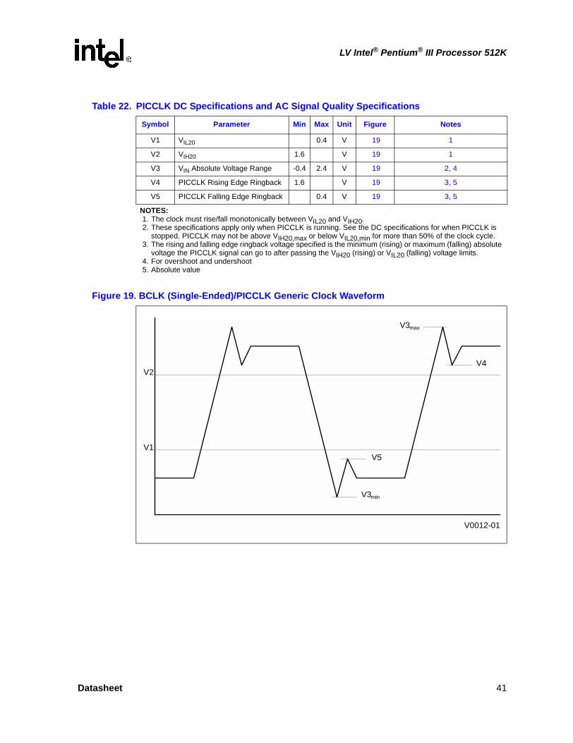
LV Intel® Pentium® III Processor 512K
Table 22. PICCLK DC Specifications and AC Signal Quality Specifications
Symbol Parameter Min Max Unit Figure Notes
V1 VIL20 0.4 V 19 1
V2 VIH20 1.6 V 19 1
V3 VIN Absolute Voltage Range -0.4 2.4 V 19 2, 4
V4 PICCLK Rising Edge Ringback 1.6 V 19 3, 5
V5 PICCLK Falling Edge Ringback 0.4 V 19 3, 5
NOTES:1. The clock must rise/fall monotonically between VIL20 and VIH20.2. These specifications apply only when PICCLK is running. See the DC specifications for when PICCLK is
stopped. PICCLK may not be above VIH20,max or below VIL20,min for more than 50% of the clock cycle.3. The rising and falling edge ringback voltage specified is the minimum (rising) or maximum (falling) absolute
voltage the PICCLK signal can go to after passing the VIH20 (rising) or VIL20 (falling) voltage limits.4. For overshoot and undershoot5. Absolute value
Figure 19. BCLK (Single-Ended)/PICCLK Generic Clock Waveform
V0012-01
V1
V2
V3max
V4
V3min
V5
Datasheet 41
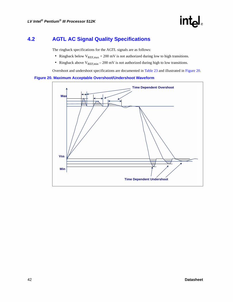
LV Intel® Pentium® III Processor 512K
4.2 AGTL AC Signal Quality Specifications
The ringback specifications for the AGTL signals are as follows:
• Ringback below VREF,max + 200 mV is not authorized during low to high transitions.
• Ringback above VREF,min – 200 mV is not authorized during high to low transitions.
Overshoot and undershoot specifications are documented in Table 23 and illustrated in Figure 20.
Figure 20. Maximum Acceptable Overshoot/Undershoot Waveform
Max
Vss
Time Dependent Overshoot
Time Dependent Undershoot
Min
42 Datasheet
LV Intel® Pentium® III Processor 512K
4.3 Non-AGTL Signal Quality Specifications
Signals driven to the LV Intel Pentium III processor 512K should meet signal quality specifications to ensure that the processor reads data properly and that incoming signals do not affect the long-term reliability of the processor. The overshoot and undershoot specifications for non AGTL signals are shown in Table 24.
Table 23. 133 MHz AGTL Signal Group Overshoot/Undershoot Toleranceat the Processor Core
Max VTT + Overshoot/UndershootMagnitude (volts)
Allowed Pulse Duration (ns) [TJ=100° C]
Activity Factor = 0.01 Activity Factor = 0.1 Activity Factor = 1
1.78 1.5 0.15 0.015
1.73 3.5 0.35 0.035
1.68 7.2 0.72 0.072
1.63 15 1.5 0.15
1.58 15 3.2 0.32
1.53 15 6.5 0.65
1.48 15 14 1.40
NOTES:1. Under no circumstances should the sum of the Max VTT and absolute value of the Overshoot/Undershoot
voltage exceed 1.78 V.2. Activity factor of 1 represents the same toggle rate as the 133-MHz clock.3. Ringbacks below VTT cannot be subtracted from overshoots. Lesser undershoot does not allocate longer or
larger overshoot. 4. Ringbacks above ground cannot be subtracted from undershoots. Lesser overshoot does not allocate
longer or larger undershoot.5. System designers are encouraged to follow Intel provided AGTL layout guidelines.6. All values are specified by design characterization and are not tested.
Table 24. Non-AGTL Signal Group Overshoot/Undershoot Tolerance at the Processor Core
Max VCmos + Overshoot/UndershootMagnitude (volts)
Allowed Pulse Duration (ns) [Tj=100° C]
Activity Factor = 0.01 Activity Factor = 0.1 Activity Factor = 1
2.38 6.5 0.65 0.065
2.33 13 1.3 0.13
2.28 29 2.9 0.29
2.23 60 6 0.6
2.18 60 12 1.2
2.13 60 26 2.6
2.08 60 56 5.6
NOTES:1. VCMOS(nominal) = 1.5 V2. Under no circumstances should the sum of the Max VCMOS and absolute value of the Overshoot/
Undershoot voltage exceed 2.38 V.3. Activity factor of 1 represents a toggle rate of 33 MHz4. System designers are encouraged to follow Intel provided non-AGTL layout guidelines.5. All values are specified by design characterization, and are not tested.
Datasheet 43
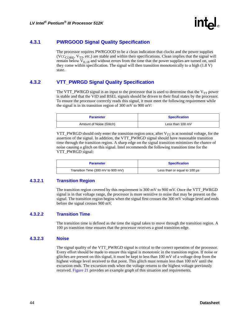
LV Intel® Pentium® III Processor 512K
4.3.1 PWRGOOD Signal Quality Specification
The processor requires PWRGOOD to be a clean indication that clocks and the power supplies (VCCCORE, VTT, etc.) are stable and within their specifications. Clean implies that the signal will remain below VIL18 and without errors from the time that the power supplies are turned on, until they come within specification. The signal will then transition monotonically to a high (1.8 V) state.
4.3.2 VTT_PWRGD Signal Quality Specification
The VTT_PWRGD signal is an input to the processor that is used to determine that the VTT power is stable and that the VID and BSEL signals should be driven to their final states by the processor. To ensure the processor correctly reads this signal, it must meet the following requirement while the signal is in its transition region of 300 mV to 900 mV:
VTT_PWRGD should only enter the transition region once, after VTT is at nominal voltage, for the assertion of the signal. In addition, the VTT_PWRGD signal should have reasonable transition time through the transition region. A sharp edge on the signal transition minimizes the chance of noise causing a glitch on this signal. Intel recommends the following transition time for the VTT_PWRGD signal:
4.3.2.1 Transition Region
The transition region covered by this requirement is 300 mV to 900 mV. Once the VTT_PWRGD signal is in that voltage range, the processor is more sensitive to noise that may be present on the signal. The transition region begins when the signal first crosses the 300 mV voltage level and ends before the signal crosses 900 mV.
4.3.2.2 Transition Time
The transition time is defined as the time the signal takes to move through the transition region. A 100 µs transition time ensures that the processor receives a good transition edge.
4.3.2.3 Noise
The signal quality of the VTT_PWRGD signal is critical to the correct operation of the processor. Every effort should be made to ensure this signal is monotonic in the transition region. If noise or glitches are present on this signal, it must be kept to less than 100 mV of a voltage drop from the highest voltage level received to that point. This glitch must remain less than 100 mV until the excursion ends. The excursion ends when the voltage returns to the highest voltage previously received. Figure 21 provides an example graph of this situation and requirements.
Parameter Specification
Amount of Noise (Glitch) Less than 100 mV
Parameter Specification
Transition Time (300 mV to 900 mV) Less than or equal to 100 µs
44 Datasheet
LV Intel® Pentium® III Processor 512K
Figure 21. Noise Estimation
Transition Region
Microseconds
Datasheet 45
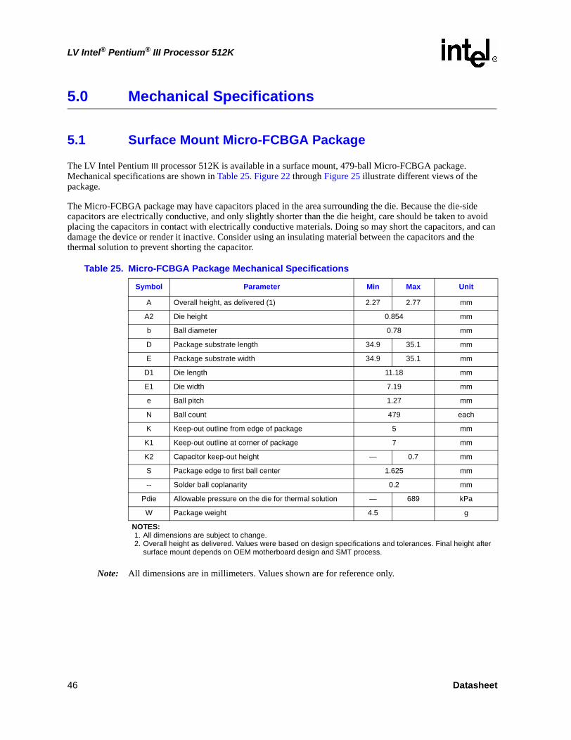
LV Intel® Pentium® III Processor 512K
5.0 Mechanical Specifications
5.1 Surface Mount Micro-FCBGA Package
The LV Intel Pentium III processor 512K is available in a surface mount, 479-ball Micro-FCBGA package. Mechanical specifications are shown in Table 25. Figure 22 through Figure 25 illustrate different views of the package.
The Micro-FCBGA package may have capacitors placed in the area surrounding the die. Because the die-side capacitors are electrically conductive, and only slightly shorter than the die height, care should be taken to avoid placing the capacitors in contact with electrically conductive materials. Doing so may short the capacitors, and can damage the device or render it inactive. Consider using an insulating material between the capacitors and the thermal solution to prevent shorting the capacitor.
Note: All dimensions are in millimeters. Values shown are for reference only.
Table 25. Micro-FCBGA Package Mechanical Specifications
Symbol Parameter Min Max Unit
A Overall height, as delivered (1) 2.27 2.77 mm
A2 Die height 0.854 mm
b Ball diameter 0.78 mm
D Package substrate length 34.9 35.1 mm
E Package substrate width 34.9 35.1 mm
D1 Die length 11.18 mm
E1 Die width 7.19 mm
e Ball pitch 1.27 mm
N Ball count 479 each
K Keep-out outline from edge of package 5 mm
K1 Keep-out outline at corner of package 7 mm
K2 Capacitor keep-out height — 0.7 mm
S Package edge to first ball center 1.625 mm
-- Solder ball coplanarity 0.2 mm
Pdie Allowable pressure on the die for thermal solution — 689 kPa
W Package weight 4.5 g
NOTES:1. All dimensions are subject to change.2. Overall height as delivered. Values were based on design specifications and tolerances. Final height after
surface mount depends on OEM motherboard design and SMT process.
46 Datasheet
LV Intel® Pentium® III Processor 512K
Figure 22. Micro-FCBGA Package – Top and Bottom Isometric Views
TOP VIEW BOTTOM VIEW
LABEL DIE
PACKAGE KEEPOUT
CAPACITOR AREA
Datasheet 47
LV Intel® Pentium® III Processor 512K
Figure 23. Micro-FCBGA Package – Top and Side Views
35 (E)
35 (D)
BALL A1 CORNER
E1
D1
A
Ø 0.78 (b)479 places
K2
SUBSTRATE KEEPOUT ZONEDO NOT CONTACT PACKAGEINSIDE THIS LINE
7 (K1)8 places
5 (K)4 places
NOTE: All dimensions in millimeters. Values shown are for reference
A2
0.20
48 Datasheet
LV Intel® Pentium® III Processor 512K
Figure 24. Micro-FCBGA Package - Bottom View
12
34 6 8 10 12 14 16 18 20 22 24 26
5 7 9 11 13 15 17 19 21 23 25
AB
C
ED
FG
HJ
KL
MN
PR
TU
VW
YAA
ABAC
ADAE
AF
NOTE: All dimensions in millimeters. Values shown are for reference only
25X 1.27(e)
25X 1.27(e)
1.625 (S)4 places
1.625 (S)4 places
Datasheet 49
LV Intel® Pentium® III Processor 512K
5.2 Signal Listings
Figure 22 is a top-side view of the ball map of the LV Intel Pentium III processor 512K with the voltage balls called out. Table 26 lists the signals in ball number order. Table 27 lists the signals in signal name order.
Figure 25. Ball Map - Top View
A10# VREF NC A31# BR0#
BR1#
A23# A27# A24# NC A35# A26# A33# A32# D0# D2# D15# D9# D7# VREF D8# D10# D11# VSS VTT
NC VSS A25# VSS A17# VSS A21# VSS A20# VSS A18# VSS A34# VSS RESET# VSS D1# VSS D4# VSS D17# VSS D18# D14# D24# VSS
NC A16# A28# VTT A19# VTT A22# VTT A30# VTT A29# VTT BERR# VTT D6# VTT D12# VTT D5# VTT NC VSS D20# VSS D30#
NC VSS A13# VSS VTT VCCCORE
VCCCORE
VCCCORE
VCCCORE
VCCCORE
VCCCORE
VCCCORE
VCCCORE
VCCCORE
VCCCORE
VCCCORE
VCCCORE
VCCCORE
VCCCORE VCCCORE
VCCCORE VCCCORE
VCCCORE
VCCCORE
VCCCORE
VCCCORE VCCCORE
VCCCORE
VCCCORE
VCCCORE
VCCCORE
VCCCORE
VCCCORE
VCCCORE
VCCCORE
VCCCORE
VCCCORE
VCCCORE
VCCCORE
VCCCORE
VCCCORE
VCCCORE
VCCCORE
VCCCORE
VCCCORE
VCCCORE
VCCCORE
VCCCORE
VCCCORE
VCCCORE
VCCCORE
VCCCORE
VCCCORE
VCCCORE
VCCCORE
VCCCORE
VCCCORE
VCCCORE
VCCCORE
VCCCORE
VCCCORE
VCCCORE
VCCCOREVCCCORE VCCCORE VCCCORE VCCCORE VCCCORE VCCCORE VCCCORE
VCCCORE VCCCORE VCCCORE VCCCORE VCCCORE VCCCORE VCCCORE VCCCORE
VCCCORE VCCCORE VCCCORE VCCCORE VCCCORE VCCCORE VCCCORE VCCCOREVSS VSS VSS VSS VSS VSS VSS VSS D3# D13# D22# NC
NC TESTHI VTT VTT VSS VSS VSS VSS VSS VSS VSS VSS D16# D23# VSS D19#
NC VSS A14# VSS VSS VSS VSS VSS VSS VSS VSS VSS VSS VSS D21# D36# D27#
A9# A5# A15# VTT VSS VSS VTT D25# VSS D32#
A12# VSS A8# VSS VSS VSS VSS D26# D29# VREF
A4# A7# A11# VTT VSS VSS VTT D34# VSS D38#
A3# VSS A6# VSS VSS VSS VSS D31# D33# D35#
REQ4# BNR# REQ1# VTT GHI# VSS VSS VTT D28# VSS D42#
VSS VSS VSS RSP# VSS VSS D39# D45# D48#
VREF PLL2 PLL1 NC VSS VSS VTT NC VSS D37#
NC VSS API# NC
NC
NC VSS VSS D49# D41# NC
REQ0# BPRI# VID4 VSS VSS VSS VTT D43# VSS D44#
REQ2# VSS DEFER# RP# VSS VSS VSS D47# D57# D51#
REQ3# HITM# RS2# VSS VSS VSS VTT D52# VSS D40#
RS1# VSS LOCK# VTT VSS VSS VSS D63# D46# D55#
TRDY# AERR# DBSY# VSS VSS VSS VTT D59# VSS D54#
DRDY# VSS RS0# VSS VSS VSS D58# D53# D60#
VREF HIT# ADS# VTT VSS VSS VSS VSS VSS VSS VSS VSS VSS VTT D62# VSS D50#
VID0 VSS AP0# PWRGOOD
VSS VSS VSS VSS VSS VSS VSS VSS VSS VSS D61# D56# VREF
BCLK VID1 A20M# VTT VSS VSS VSS VSS VSS VSS VSS VSS VSS VTT DEP3# VSS DEP6#
BCLK# /CLKREF
VSS SMI#_REF
VCMOS
_REFVCMOS
VTT TDI VTT IGNNE# TCK
THERM
TDO VTT NC VTT LINT0 PICD1 VTT PICD0 VTT BPM1# BPM0# NC DEP7# DEP1# DEP5#
VSS VID2 VTT STPCLK# VSS INIT# VSS NC VSS VSSTRIP#
BSEL0 VSS LINT1 VSS VSS VTT VSS BP3# VSS PRDY# VSS DEP0# DEP2# VSS
VTT VTT VID3 IERR# FLUSH# FERR# SLP#TMS VREF BSEL1 TESTHI TRST#THERMDPTHERMDN
NC
NCHCTRL
RTTCTRL
SLEWCTRL
NC PREQ# PICCLK VREF BP2# BINIT# DEP4# VSS VSS
A
B
C
D
E
F
G
H
J
K
L
M
N
P
R
T
U
V
W
Y
AA
AB
AC
AD
AE
AF
1 2 3 4 5 6 7 8 9 10 11 12 13 14 15 16 17 18 19 20 21 22 23 24 25 26
VTT_PWRGD
A
B
C
D
E
F
G
H
J
K
L
M
N
P
R
T
U
V
W
Y
AA
AB
AC
AD
AE
AF
1 2 3 4 5 6 7 8 9 10 11 12 13 14 15 16 17 18 19 20 21 22 23 24 25 26
VCCCORE VSS OtherVTT
TESTLO
TESTLO
NC
NC
VID25mV
50 Datasheet
Mechanical Specifications
Table 26. Signal List by Ball Number
No. Signal Name
A2 NC
A3 A10#
A4 VREF
A5 NC
A6 A31#
A7 BR0#
A8 A23#
A9 A27#
A10 A24#
A11 NC
A12 A35#
A13 A26#
A14 A33#
A15 A32#
A16 D0#
A17 D2#
A18 D15#
A19 D9#
A20 D7#
A21 VREF
A22 D8#
A23 D10#
A24 D11#
A25 VSS
A26 VTT
B1 NC
B2 VSS
B3 A25#
B4 VSS
B5 A17#
B6 VSS
B7 A21#
B8 VSS
B9 A20#
B10 VSS
B11 A18#
B12 VSS
B13 A34#
B14 VSS
B15 RESET#
B16 VSS
B17 D1#
B18 VSS
B19 D4#
B20 VSS
B21 D17#
B22 VSS
B23 D18#
B24 D14#
B25 D24#
B26 VSS
C1 NC
C2 A16#
C3 A28#
C4 BR1#
C5 VTT
C6 A19#
C7 VTT
C8 A22#
C9 VTT
C10 A30#
C11 VTT
C12 A29#
C13 VTT
C14 BERR#
C15 VTT
C16 D6#
C17 VTT
C18 D12#
C19 VTT
C20 D5#
C21 VTT
C22 NC
C23 VSS
C24 D20#
C25 VSS
C26 D30#
D1 NC
D2 VSS
D3 A13#
D4 VSS
D5 VTT
Table 26. Signal List by Ball Number
No. Signal Name
D6 VCCCORE
D7 VSS
D8 VCCCORE
D9 VSS
D10 VCCCORE
D11 VSS
D12 VCCCORE
D13 VSS
D14 VCCCORE
D15 VSS
D16 VCCCORE
D17 VSS
D18 VCCCORE
D19 VSS
D20 VCCCORE
D21 VSS
D22 VCCCORE
D23 D3#
D24 D13#
D25 D22#
D26 NC
E1 NC
E2 TESTHI
E3 VTT_PWRGD
E4 VTT
E5 VCCCORE
E6 VTT
E7 VCCCORE
E8 VSS
E9 VCCCORE
E10 VSS
E11 VCCCORE
E12 VSS
E13 VCCCORE
E14 VSS
E15 VCCCORE
E16 VSS
E17 VCCCORE
E18 VSS
E19 VCCCORE
E20 VSS
Table 26. Signal List by Ball Number
No. Signal Name
E21 VCCCORE
E22 VSS
E23 D16#
E24 D23#
E25 VSS
E26 D19#
F1 NC
F2 VSS
F3 A14#
F4 VSS
F5 VSS
F6 VCCCORE
F7 VSS
F8 VCCCORE
F9 VSS
F10 VCCCORE
F11 VSS
F12 VCCCORE
F13 VSS
F14 VCCCORE
F15 VSS
F16 VCCCORE
F17 VSS
F18 VCCCORE
F19 VSS
F20 VCCCORE
F21 VSS
F22 VCCCORE
F23 VSS
F24 D21#
F25 D36#
F26 D27#
G1 A9#
G2 A5#
G3 A15#
G4 VTT
G5 VCCCORE
G6 VSS
G21 VCCCORE
G22 VSS
G23 VTT
Table 26. Signal List by Ball Number
No. Signal Name
Datasheet 51
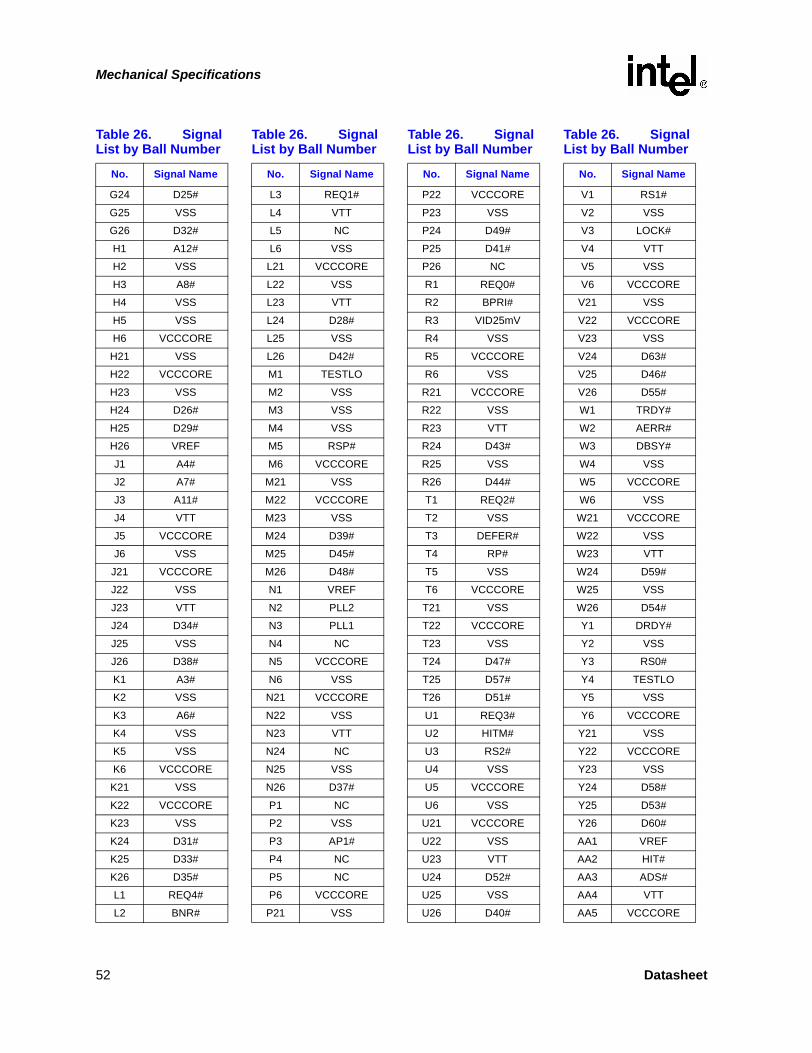
Mechanical Specifications
G24 D25#
G25 VSS
G26 D32#
H1 A12#
H2 VSS
H3 A8#
H4 VSS
H5 VSS
H6 VCCCORE
H21 VSS
H22 VCCCORE
H23 VSS
H24 D26#
H25 D29#
H26 VREF
J1 A4#
J2 A7#
J3 A11#
J4 VTT
J5 VCCCORE
J6 VSS
J21 VCCCORE
J22 VSS
J23 VTT
J24 D34#
J25 VSS
J26 D38#
K1 A3#
K2 VSS
K3 A6#
K4 VSS
K5 VSS
K6 VCCCORE
K21 VSS
K22 VCCCORE
K23 VSS
K24 D31#
K25 D33#
K26 D35#
L1 REQ4#
L2 BNR#
Table 26. Signal List by Ball Number
No. Signal Name
L3 REQ1#
L4 VTT
L5 NC
L6 VSS
L21 VCCCORE
L22 VSS
L23 VTT
L24 D28#
L25 VSS
L26 D42#
M1 TESTLO
M2 VSS
M3 VSS
M4 VSS
M5 RSP#
M6 VCCCORE
M21 VSS
M22 VCCCORE
M23 VSS
M24 D39#
M25 D45#
M26 D48#
N1 VREF
N2 PLL2
N3 PLL1
N4 NC
N5 VCCCORE
N6 VSS
N21 VCCCORE
N22 VSS
N23 VTT
N24 NC
N25 VSS
N26 D37#
P1 NC
P2 VSS
P3 AP1#
P4 NC
P5 NC
P6 VCCCORE
P21 VSS
Table 26. Signal List by Ball Number
No. Signal Name
P22 VCCCORE
P23 VSS
P24 D49#
P25 D41#
P26 NC
R1 REQ0#
R2 BPRI#
R3 VID25mV
R4 VSS
R5 VCCCORE
R6 VSS
R21 VCCCORE
R22 VSS
R23 VTT
R24 D43#
R25 VSS
R26 D44#
T1 REQ2#
T2 VSS
T3 DEFER#
T4 RP#
T5 VSS
T6 VCCCORE
T21 VSS
T22 VCCCORE
T23 VSS
T24 D47#
T25 D57#
T26 D51#
U1 REQ3#
U2 HITM#
U3 RS2#
U4 VSS
U5 VCCCORE
U6 VSS
U21 VCCCORE
U22 VSS
U23 VTT
U24 D52#
U25 VSS
U26 D40#
Table 26. Signal List by Ball Number
No. Signal Name
V1 RS1#
V2 VSS
V3 LOCK#
V4 VTT
V5 VSS
V6 VCCCORE
V21 VSS
V22 VCCCORE
V23 VSS
V24 D63#
V25 D46#
V26 D55#
W1 TRDY#
W2 AERR#
W3 DBSY#
W4 VSS
W5 VCCCORE
W6 VSS
W21 VCCCORE
W22 VSS
W23 VTT
W24 D59#
W25 VSS
W26 D54#
Y1 DRDY#
Y2 VSS
Y3 RS0#
Y4 TESTLO
Y5 VSS
Y6 VCCCORE
Y21 VSS
Y22 VCCCORE
Y23 VSS
Y24 D58#
Y25 D53#
Y26 D60#
AA1 VREF
AA2 HIT#
AA3 ADS#
AA4 VTT
AA5 VCCCORE
Table 26. Signal List by Ball Number
No. Signal Name
52 Datasheet
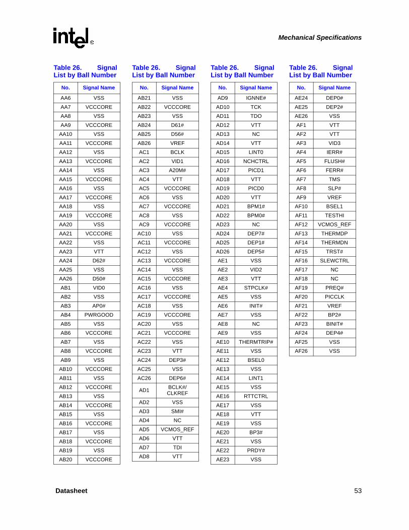
Mechanical Specifications
AA6 VSS
AA7 VCCCORE
AA8 VSS
AA9 VCCCORE
AA10 VSS
AA11 VCCCORE
AA12 VSS
AA13 VCCCORE
AA14 VSS
AA15 VCCCORE
AA16 VSS
AA17 VCCCORE
AA18 VSS
AA19 VCCCORE
AA20 VSS
AA21 VCCCORE
AA22 VSS
AA23 VTT
AA24 D62#
AA25 VSS
AA26 D50#
AB1 VID0
AB2 VSS
AB3 AP0#
AB4 PWRGOOD
AB5 VSS
AB6 VCCCORE
AB7 VSS
AB8 VCCCORE
AB9 VSS
AB10 VCCCORE
AB11 VSS
AB12 VCCCORE
AB13 VSS
AB14 VCCCORE
AB15 VSS
AB16 VCCCORE
AB17 VSS
AB18 VCCCORE
AB19 VSS
AB20 VCCCORE
Table 26. Signal List by Ball Number
No. Signal Name
AB21 VSS
AB22 VCCCORE
AB23 VSS
AB24 D61#
AB25 D56#
AB26 VREF
AC1 BCLK
AC2 VID1
AC3 A20M#
AC4 VTT
AC5 VCCCORE
AC6 VSS
AC7 VCCCORE
AC8 VSS
AC9 VCCCORE
AC10 VSS
AC11 VCCCORE
AC12 VSS
AC13 VCCCORE
AC14 VSS
AC15 VCCCORE
AC16 VSS
AC17 VCCCORE
AC18 VSS
AC19 VCCCORE
AC20 VSS
AC21 VCCCORE
AC22 VSS
AC23 VTT
AC24 DEP3#
AC25 VSS
AC26 DEP6#
AD1 BCLK#/CLKREF
AD2 VSS
AD3 SMI#
AD4 NC
AD5 VCMOS_REF
AD6 VTT
AD7 TDI
AD8 VTT
Table 26. Signal List by Ball Number
No. Signal Name
AD9 IGNNE#
AD10 TCK
AD11 TDO
AD12 VTT
AD13 NC
AD14 VTT
AD15 LINT0
AD16 NCHCTRL
AD17 PICD1
AD18 VTT
AD19 PICD0
AD20 VTT
AD21 BPM1#
AD22 BPM0#
AD23 NC
AD24 DEP7#
AD25 DEP1#
AD26 DEP5#
AE1 VSS
AE2 VID2
AE3 VTT
AE4 STPCLK#
AE5 VSS
AE6 INIT#
AE7 VSS
AE8 NC
AE9 VSS
AE10 THERMTRIP#
AE11 VSS
AE12 BSEL0
AE13 VSS
AE14 LINT1
AE15 VSS
AE16 RTTCTRL
AE17 VSS
AE18 VTT
AE19 VSS
AE20 BP3#
AE21 VSS
AE22 PRDY#
AE23 VSS
Table 26. Signal List by Ball Number
No. Signal Name
AE24 DEP0#
AE25 DEP2#
AE26 VSS
AF1 VTT
AF2 VTT
AF3 VID3
AF4 IERR#
AF5 FLUSH#
AF6 FERR#
AF7 TMS
AF8 SLP#
AF9 VREF
AF10 BSEL1
AF11 TESTHI
AF12 VCMOS_REF
AF13 THERMDP
AF14 THERMDN
AF15 TRST#
AF16 SLEWCTRL
AF17 NC
AF18 NC
AF19 PREQ#
AF20 PICCLK
AF21 VREF
AF22 BP2#
AF23 BINIT#
AF24 DEP4#
AF25 VSS
AF26 VSS
Table 26. Signal List by Ball Number
No. Signal Name
Datasheet 53
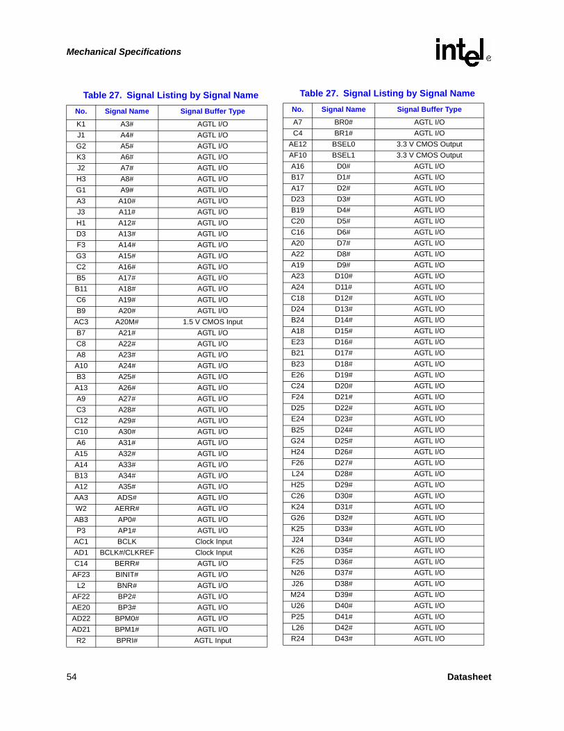
Mechanical Specifications
Table 27. Signal Listing by Signal NameNo. Signal Name Signal Buffer Type
K1 A3# AGTL I/OJ1 A4# AGTL I/OG2 A5# AGTL I/OK3 A6# AGTL I/OJ2 A7# AGTL I/OH3 A8# AGTL I/OG1 A9# AGTL I/OA3 A10# AGTL I/OJ3 A11# AGTL I/OH1 A12# AGTL I/OD3 A13# AGTL I/OF3 A14# AGTL I/OG3 A15# AGTL I/OC2 A16# AGTL I/OB5 A17# AGTL I/OB11 A18# AGTL I/OC6 A19# AGTL I/OB9 A20# AGTL I/O
AC3 A20M# 1.5 V CMOS InputB7 A21# AGTL I/OC8 A22# AGTL I/OA8 A23# AGTL I/OA10 A24# AGTL I/OB3 A25# AGTL I/OA13 A26# AGTL I/OA9 A27# AGTL I/OC3 A28# AGTL I/OC12 A29# AGTL I/OC10 A30# AGTL I/OA6 A31# AGTL I/OA15 A32# AGTL I/OA14 A33# AGTL I/OB13 A34# AGTL I/OA12 A35# AGTL I/OAA3 ADS# AGTL I/OW2 AERR# AGTL I/OAB3 AP0# AGTL I/OP3 AP1# AGTL I/O
AC1 BCLK Clock InputAD1 BCLK#/CLKREF Clock InputC14 BERR# AGTL I/O
AF23 BINIT# AGTL I/OL2 BNR# AGTL I/O
AF22 BP2# AGTL I/OAE20 BP3# AGTL I/OAD22 BPM0# AGTL I/OAD21 BPM1# AGTL I/O
R2 BPRI# AGTL Input
A7 BR0# AGTL I/OC4 BR1# AGTL I/O
AE12 BSEL0 3.3 V CMOS OutputAF10 BSEL1 3.3 V CMOS OutputA16 D0# AGTL I/OB17 D1# AGTL I/OA17 D2# AGTL I/OD23 D3# AGTL I/OB19 D4# AGTL I/OC20 D5# AGTL I/OC16 D6# AGTL I/OA20 D7# AGTL I/OA22 D8# AGTL I/OA19 D9# AGTL I/OA23 D10# AGTL I/OA24 D11# AGTL I/OC18 D12# AGTL I/OD24 D13# AGTL I/OB24 D14# AGTL I/OA18 D15# AGTL I/OE23 D16# AGTL I/OB21 D17# AGTL I/OB23 D18# AGTL I/OE26 D19# AGTL I/OC24 D20# AGTL I/OF24 D21# AGTL I/OD25 D22# AGTL I/OE24 D23# AGTL I/OB25 D24# AGTL I/OG24 D25# AGTL I/OH24 D26# AGTL I/OF26 D27# AGTL I/OL24 D28# AGTL I/OH25 D29# AGTL I/OC26 D30# AGTL I/OK24 D31# AGTL I/OG26 D32# AGTL I/OK25 D33# AGTL I/OJ24 D34# AGTL I/OK26 D35# AGTL I/OF25 D36# AGTL I/ON26 D37# AGTL I/OJ26 D38# AGTL I/OM24 D39# AGTL I/OU26 D40# AGTL I/OP25 D41# AGTL I/OL26 D42# AGTL I/OR24 D43# AGTL I/O
Table 27. Signal Listing by Signal NameNo. Signal Name Signal Buffer Type
54 Datasheet

Mechanical Specifications
R26 D44# AGTL I/OM25 D45# AGTL I/OV25 D46# AGTL I/OT24 D47# AGTL I/OM26 D48# AGTL I/OP24 D49# AGTL I/O
AA26 D50# AGTL I/OT26 D51# AGTL I/OU24 D52# AGTL I/OY25 D53# AGTL I/OW26 D54# AGTL I/OV26 D55# AGTL I/O
AB25 D56# AGTL I/OT25 D57# AGTL I/OY24 D58# AGTL I/OW24 D59# AGTL I/OY26 D60# AGTL I/O
AB24 D61# AGTL I/OAA24 D62# AGTL I/OV24 D63# AGTL I/OW3 DBSY# AGTL I/OT3 DEFER# AGTL Input
AE24 DEP0# AGTL I/OAD25 DEP1# AGTL I/OAE25 DEP2# AGTL I/OAC24 DEP3# AGTL I/OAF24 DEP4# AGTL I/OAD26 DEP5# AGTL I/OAC26 DEP6# AGTL I/OAD24 DEP7# AGTL I/O
Y1 DRDY# AGTL I/OAF6 FERR# 1.5 V Open Drain OutputAF5 FLUSH# 1.5 V CMOS InputAA2 HIT# AGTL I/OU2 HITM# AGTL I/O
AF4 IERR# 1.5 V Open Drain OutputAD9 IGNNE# 1.5 V CMOS InputAE6 INIT# 1.5 V CMOS Input
AD15 INTR/LINT0 1.5 V CMOS InputV3 LOCK# AGTL I/O
AD16 NCHCTRL AGTL impedance controlAE14 NMI/LINT1 1.5 V CMOS InputAF20 PICCLK 1.8 V APIC Clock InputAD19 PICD0 1.5 V Open Drain I/OAD17 PICD1 1.5 V Open Drain I/O
N3 PLL1 PLL Analog VoltageN2 PLL2 PLL Analog Voltage
AE22 PRDY# AGTL Output
Table 27. Signal Listing by Signal NameNo. Signal Name Signal Buffer Type
AF19 PREQ# 1.5 V CMOS InputAB4 PWRGOOD 1.8 V CMOS InputR1 REQ0# AGTL I/OL3 REQ1# AGTL I/OT1 REQ2# AGTL I/OU1 REQ3# AGTL I/OL1 REQ4# AGTL I/O
B15 RESET# AGTL InputT4 RP# AGTL I/OY3 RS0# AGTL I/OV1 RS1# AGTL I/OU3 RS2# AGTL I/OM5 RSP# AGTL Input
AE16 RTTCTRL AGTL Pull-up ControlAF16 SLEWCTRL AGTL ControlAF8 SLP# 1.5 V CMOS InputAD3 SMI# 1.5 V CMOS InputAE4 STPCLK# 1.5 V CMOS Input
AD10 TCK 1.5 V JTAG Clock InputAD7 TDI JTAG InputAD11 TDO JTAG Output
E2 TESTHI Test Use OnlyAF11 TESTHI Test Use OnlyM1 TESTLO Test Use OnlyY4 TESTLO Test Use Only
AF14 THERMDN Thermal Diode CathodeAF13 THERMDP Thermal Diode AnodeAE10 THERMTRIP# 1.5 V Open Drain OutputAF7 TMS JTAG InputW1 TRDY# AGTL I/O
AF15 TRST# JTAG InputAD5 VCMOS_REF CMOS Reference VoltageAF12 VCMOS_REF CMOS Reference VoltageAB1 VID0 Voltage IdentificationAC2 VID1 Voltage IdentificationAE2 VID2 Voltage IdentificationR3 VID25mV Voltage IdentificationAF3 VID3 Voltage IdentificationA4 VREF AGTL Reference VoltageA21 VREF AGTL Reference VoltageN1 VREF AGTL Reference VoltageAF9 VREF AGTL Reference Voltage
AF21 VREF AGTL Reference VoltageAA1 VREF AGTL Reference Voltage
AB26 VREF AGTL Reference VoltageH26 VREF AGTL Reference VoltageE3 VTT_PWRGD VTT power good signal
Table 27. Signal Listing by Signal NameNo. Signal Name Signal Buffer Type
Datasheet 55
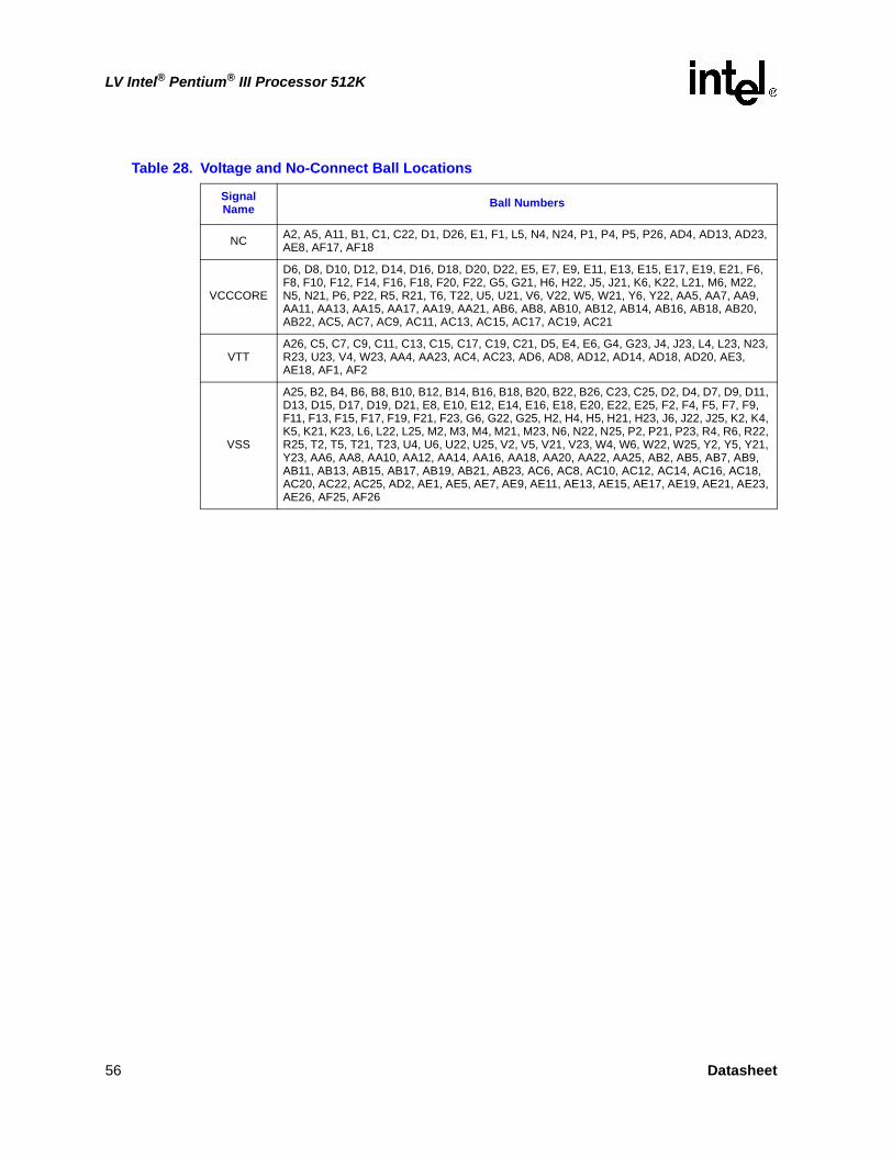
LV Intel® Pentium® III Processor 512K
Table 28. Voltage and No-Connect Ball Locations
SignalName Ball Numbers
NC A2, A5, A11, B1, C1, C22, D1, D26, E1, F1, L5, N4, N24, P1, P4, P5, P26, AD4, AD13, AD23, AE8, AF17, AF18
VCCCORE
D6, D8, D10, D12, D14, D16, D18, D20, D22, E5, E7, E9, E11, E13, E15, E17, E19, E21, F6, F8, F10, F12, F14, F16, F18, F20, F22, G5, G21, H6, H22, J5, J21, K6, K22, L21, M6, M22, N5, N21, P6, P22, R5, R21, T6, T22, U5, U21, V6, V22, W5, W21, Y6, Y22, AA5, AA7, AA9, AA11, AA13, AA15, AA17, AA19, AA21, AB6, AB8, AB10, AB12, AB14, AB16, AB18, AB20, AB22, AC5, AC7, AC9, AC11, AC13, AC15, AC17, AC19, AC21
VTTA26, C5, C7, C9, C11, C13, C15, C17, C19, C21, D5, E4, E6, G4, G23, J4, J23, L4, L23, N23, R23, U23, V4, W23, AA4, AA23, AC4, AC23, AD6, AD8, AD12, AD14, AD18, AD20, AE3, AE18, AF1, AF2
VSS
A25, B2, B4, B6, B8, B10, B12, B14, B16, B18, B20, B22, B26, C23, C25, D2, D4, D7, D9, D11, D13, D15, D17, D19, D21, E8, E10, E12, E14, E16, E18, E20, E22, E25, F2, F4, F5, F7, F9, F11, F13, F15, F17, F19, F21, F23, G6, G22, G25, H2, H4, H5, H21, H23, J6, J22, J25, K2, K4, K5, K21, K23, L6, L22, L25, M2, M3, M4, M21, M23, N6, N22, N25, P2, P21, P23, R4, R6, R22, R25, T2, T5, T21, T23, U4, U6, U22, U25, V2, V5, V21, V23, W4, W6, W22, W25, Y2, Y5, Y21, Y23, AA6, AA8, AA10, AA12, AA14, AA16, AA18, AA20, AA22, AA25, AB2, AB5, AB7, AB9, AB11, AB13, AB15, AB17, AB19, AB21, AB23, AC6, AC8, AC10, AC12, AC14, AC16, AC18, AC20, AC22, AC25, AD2, AE1, AE5, AE7, AE9, AE11, AE13, AE15, AE17, AE19, AE21, AE23, AE26, AF25, AF26
56 Datasheet
LV Intel® Pentium® III Processor 512K
6.0 Thermal Specifications and Design Considerations
This section provides needed data for designing a thermal solution. The LV Intel Pentium III processor 512K uses micro flip-chip ball-grid-array packaging technology and has a junction temperature (TJ) specified at 100º C.
6.1 Thermal Specifications
Table 29 provides the thermal design power dissipation and maximum temperatures for the LV Intel Pentium III processor 512K. Systems should design for the highest possible processor power, even if a processor with a lower thermal dissipation is planned. A thermal solution should be designed to ensure the junction temperature never exceeds these specifications.
6.1.1 THERMTRIP# Requirement
In the event the processor drives the THERMTRIP# signal active during valid operation, both the VCCCORE and VTT supplies to the processor must be turned off to prevent thermal runaway of the processor. Valid operation refers to the operating conditions where the THERMTRIP# signal is guaranteed valid. The time required from THERMTRIP# asserted to VCCCORE rail at 1/2 nominal is 5 seconds and THERMTRIP# asserted to VTT rail at 1/2 nominal is 5 seconds.
Table 29. LV Intel Pentium III Processor 512K Thermal Design Power
Processor Core Frequency
(MHz)
Processor Core Voltage
(V)Processor Signature
L2 Cache Size(Kbytes)
Thermal Design Power1, 2
(Max, in W) Maximum TJ (°C)
800 1.1506B206B4
512 10.63 100
933 1.1506B4
512 11.61 100
1000 1.1506B4
512 12.1 100
NOTES:1. These values are specified at nominal VccCORE for the processor balls.2. Processor power includes the power dissipated by the processor core, the L2 cache, and the AGTL bus termination. The
maximum power for each of these components does not occur simultaneously.
Table 30. THERMTRIP# Time Requirement
Power Rail Power Target Time required for power drop
VCCCORE 1/2 Nominal VCCCORE 5 seconds
VTT 1/2 Nominal VTT 5 seconds
NOTE: Once VCCCORE and VTT supplies are turned off the THERMTRIP# signal will be deactivated. System logic should ensure no “unsafe” power cycling occurs due to this deassertion.
Datasheet 57
LV Intel® Pentium® III Processor 512K
6.1.2 Thermal Diode
The LV Intel Pentium III processor 512K has an on-die thermal diode that can be used to monitor the die temperature (TJ). A thermal sensor located on the motherboard, or a stand-alone measurement kit, may monitor the die temperature of the processor for thermal management or instrumentation purposes. Table 31 and Table 32 provide the diode interface and specifications.
Note: The reading of the thermal sensor connected to the thermal diode will not necessarily reflect the temperature of the hottest location on the die. This is due to inaccuracies in the thermal sensor, on-die temperature gradients between the location of the thermal diode and the hottest location on the die, and time based variations in the die temperature measurement. Time based variations can occur when the sampling rate of the thermal diode (by the thermal sensor) is slower than the rate at which the TJ temperature can change.
Table 31. Thermal Diode Interface
Ball Name Ball Number Description
THERMDP AF13 Thermal diode anode
THERMDN AF14 Thermal diode cathode
Table 32. Thermal Diode Parameters
Symbol Parameter1 Min Typ Max Unit Notes
n Diode Ideality Factor (5-150 µA) 1.0011 1.0067 1.0122 1, 2, 3, 4, 6
n Diode Ideality Factor (5-300 µA) 1.0003 1.0091 1.0178 1, 2, 3, 5, 6
NOTES:1. Intel does not support or recommend operation of the thermal diode under reverse bias. Intel does not
support or recommend operation of the thermal diode when the processor power supplies are not within their specified tolerance range.
2. Characterized at 100° C3. Not 100% tested. Specified by design/characterization.4. Specified for forward bias current = 5 µA (min) and 150 µA (max)5. Specified for forward bias current = 5 µA (min) and 300 µA (max)6. The ideality factor, n, represents the deviation from ideal diode behavior as exemplified by the diode
equation:
where IS = saturation current, q = electronic charge, VD = voltage across the diode, k = Boltzmann Constant, and T = absolute temperature (Kelvin).
IFW = IS eqVD
nkT – 1
58 Datasheet
LV Intel® Pentium® III Processor 512K
7.0 Processor Interface
7.1 Alphabetical Signals Reference
Table 33. Signal Description (Sheet 1 of 8)
Name Type Description
A20M# I
If the A20M# (Address-20 Mask) input signal is asserted, the processor masks physical address bit 20 (A20#) before looking up a line in any internal cache and before driving a read/write transaction on the bus. Asserting A20M# emulates the 8086 processor's address wrap-around at the 1 MB boundary. Assertion of A20M# is only supported in real mode.A20M# is an asynchronous signal. However, to ensure recognition of this signal following an I/O write instruction, it must be valid along with the TRDY# assertion of the corresponding I/O Write bus transaction.
A[35:3]# I/O
The A[35:3]# (Address) signals define a 236-byte physical memory address space. When ADS# is active, these balls transmit the address of a transaction; when ADS# is inactive, these balls transmit transaction type information. These signals must connect the appropriate balls of all agents on the processor system bus. The A[35:24]# signals are parity-protected by the AP1# parity signal, and the A[23:3]# signals are parity-protected by the AP0# parity signal.On the active-to-inactive transition of RESET#, the processors sample the A[35:3]# balls to determine their power-on configuration. See the P6 Family of Processors Hardware Developer’s Manual for details.
ADS# I/O
The ADS# (Address Strobe) signal is asserted to indicate the validity of the transaction address on the A[35:3]# balls. All bus agents observe the ADS# activation to begin parity checking, protocol checking, address decode, internal snoop, or deferred reply ID match operations associated with the new transaction. This signal must connect the appropriate balls on all processor system bus agents.
AERR# I/O
The AERR# (Address Parity Error) signal is observed and driven by all processor system bus agents, and if used, must connect the appropriate balls on all processor system bus agents. AERR# observation is optionally enabled during power-on configuration; if enabled, a valid assertion of AERR# aborts the current transaction.If AERR# observation is disabled during power-on configuration, a central agent may handle an assertion of AERR# as appropriate to the error handling architecture of the system.
AP[1:0]# I/O
The AP[1:0]# (Address Parity) signals are driven by the request initiator along with ADS#, A[35:3]#, REQ[4:0]#, and RP#. AP1# covers A[35:24]#, and AP0# covers A[23:3]#. A correct parity signal is high if an even number of covered signals are low and low if an odd number of covered signals are low. This allows parity to be high when all the covered signals are high. AP[1:0]# should connect the appropriate balls of all processor system bus agents.
BCLK/BCLK# I
The BCLK (Bus Clock) and BCLK# (for differential clock) signals determines the bus frequency. All processor system bus agents must receive this signal to drive their outputs and latch their inputs on the rising edge of BCLK. For differential clocking, all processor system bus agents must receive this signal to drive their outputs and latch their inputs on the BCLK and BCLK# crossing point.All external timing parameters are specified with respect to the BCLK signal.
Datasheet 59
LV Intel® Pentium® III Processor 512K
BERR# I/O
The BERR# (Bus Error) signal is asserted to indicate an unrecoverable error without a bus protocol violation. It may be driven by all processor system bus agents, and must connect the appropriate balls of all such agents, if used. However, the LV Intel Pentium III processor 512K does not observe assertions of the BERR# signal.BERR# assertion conditions are configurable at a system level. Assertion options are defined by the following options:
• Enabled or disabled.• Asserted optionally for internal errors along with IERR#.• Asserted optionally by the request initiator of a bus transaction after it observes
an error.• Asserted by any bus agent when it observes an error in a bus transaction.
BINIT# I/O
The BINIT# (Bus Initialization) signal may be observed and driven by all processor system bus agents. When used, it must connect the appropriate balls of all such agents. If the BINIT# driver is enabled during power on configuration, BINIT# is asserted to signal any bus condition that prevents reliable future information.If BINIT# observation is enabled during power-on configuration, and BINIT# is sampled asserted, all bus state machines are reset and any data that is in transit is lost. All agents reset their rotating ID for bus arbitration to the state after Reset, and internal count information is lost. The L1 and L2 caches are not affected.If BINIT# observation is disabled during power-on configuration, a central agent may handle an assertion of BINIT# as appropriate to the error handling architecture of the system.
BNR# I/O
The BNR# (Block Next Request) signal is used to assert a bus stall by any bus agent who is unable to accept new bus transactions. During a bus stall, the current bus owner cannot issue any new transactions.Since multiple agents might need to request a bus stall at the same time, BNR# is a wire-OR signal that must connect the appropriate balls of all processor system bus agents. In order to avoid wire-OR glitches associated with simultaneous edge transitions driven by multiple drivers, BNR# is activated on specific clock edges and sampled on specific clock edges.
BP[3:2]# I/O The BP[3:2]# (Breakpoint) signals are outputs from the processor that indicate the status of breakpoints.
BPM[1:0]# I/O
The BPM[1:0]# (Breakpoint Monitor) signals are breakpoint and performance monitor signals. They are outputs from the processor that indicate the status of breakpoints and programmable counters used for monitoring processor performance.
BPRI# I
The BPRI# (Bus Priority Request) signal is used to arbitrate for ownership of the processor system bus. It must connect the appropriate balls of all processor system bus agents. Observing BPRI# active (as asserted by the priority agent) causes all other agents to stop issuing new requests, unless such requests are part of an ongoing locked operation. The priority agent keeps BPRI# asserted until all of its requests are completed. It then releases the bus by deasserting BPRI#.
Table 33. Signal Description (Sheet 2 of 8)
Name Type Description
60 Datasheet
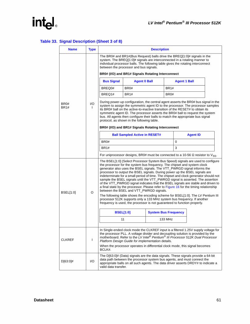
LV Intel® Pentium® III Processor 512K
BR0#BR1#
I/OI
The BR0# and BR1#(Bus Request) balls drive the BREQ[1:0]# signals in the system. The BREQ[1:0]# signals are interconnected in a rotating manner to individual processor balls. The following table gives the rotating interconnect between the processor and bus signals.
During power-up configuration, the central agent asserts the BR0# bus signal in the system to assign the symmetric agent ID to the processor. The processor samples its BR0# ball on the active-to-inactive transition of the RESET# to obtain its symmetric agent ID. The processor asserts the BR0# ball to request the system bus. All agents then configure their balls to match the appropriate bus signal protocol, as shown in the following table.
For uniprocessor designs, BR0# must be connected to a 10-56 Ω resistor to VSS.
BSEL[1:0] O
The BSEL[1:0] (Select Processor System Bus Speed) signals are used to configure the processor for the system bus frequency. The chipset and system clock generator also uses the BSEL signals. The VTT_PWRGD signal informs the processor to output the BSEL signals. During power up the BSEL signals are indeterminate for a small period of time. The chipset and clock generator should not sample the BSEL signals until the VTT_PWRGD signal is asserted. The assertion of the VTT_PWRGD signal indicates that the BSEL signals are stable and driven to a final state by the processor. Please refer to Figure 16 for the timing relationship between the BSEL and VTT_PWRGD signals.The following table shows the encoding scheme for BSEL[1:0]. The LV Pentium III processor 512K supports only a 133 MHz system bus frequency. If another frequency is used, the processor is not guaranteed to function properly.
CLKREF I
In Single-ended clock mode the CLKREF input is a filtered 1.25V supply voltage for the processor PLL. A voltage divider and decoupling solution is provided by the motherboard. Refer to the LV Intel® Pentium® III Processor 512K Dual Processor Platform Design Guide for implementation details.When the processor operates in differential clock mode, this signal becomes BCLK#.
D[63:0]# I/O
The D[63:0]# (Data) signals are the data signals. These signals provide a 64-bit data path between the processor system bus agents, and must connect the appropriate balls on all such agents. The data driver asserts DRDY# to indicate a valid data transfer.
Table 33. Signal Description (Sheet 3 of 8)
Name Type Description
BR0# (I/O) and BR1# Signals Rotating Interconnect
Bus Signal Agent 0 Ball Agent 1 Ball
BREQ0# BR0# BR1#
BREQ1# BR1# BR0#
BR0# (I/O) and BR1# Signals Rotating Interconnect
Ball Sampled Active in RESET# Agent ID
BR0# 0
BR1# 3
BSEL[1:0] System Bus Frequency
11 133 MHz
Datasheet 61
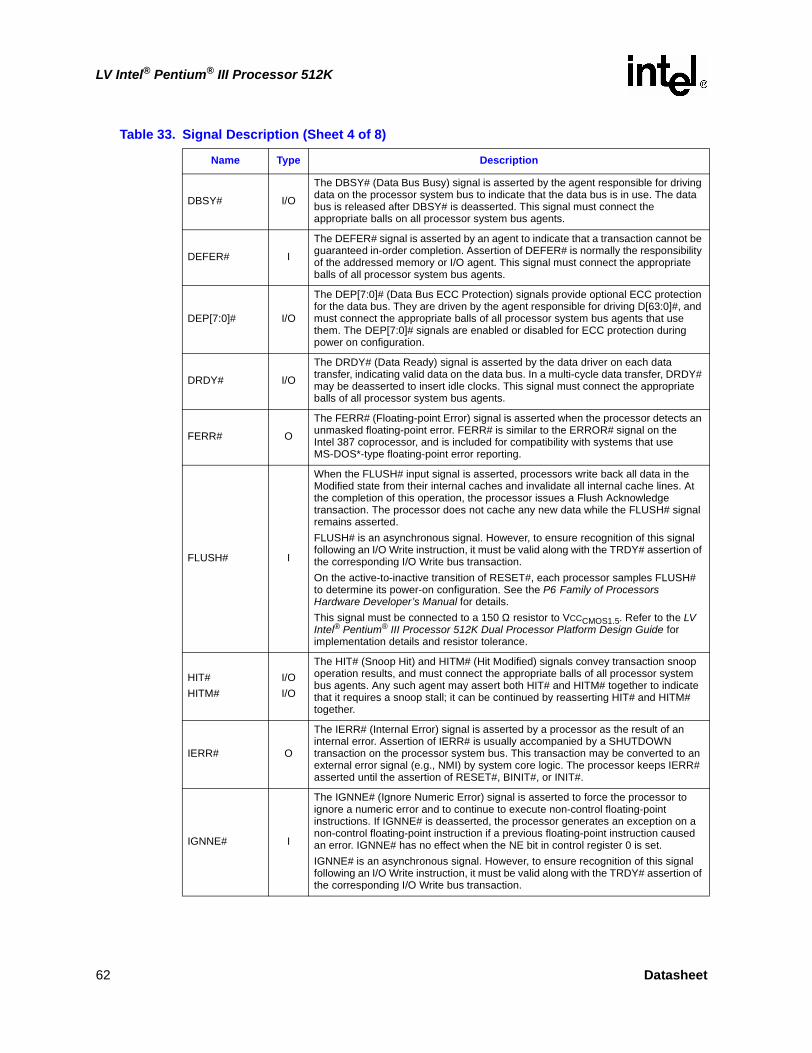
LV Intel® Pentium® III Processor 512K
DBSY# I/O
The DBSY# (Data Bus Busy) signal is asserted by the agent responsible for driving data on the processor system bus to indicate that the data bus is in use. The data bus is released after DBSY# is deasserted. This signal must connect the appropriate balls on all processor system bus agents.
DEFER# I
The DEFER# signal is asserted by an agent to indicate that a transaction cannot be guaranteed in-order completion. Assertion of DEFER# is normally the responsibility of the addressed memory or I/O agent. This signal must connect the appropriate balls of all processor system bus agents.
DEP[7:0]# I/O
The DEP[7:0]# (Data Bus ECC Protection) signals provide optional ECC protection for the data bus. They are driven by the agent responsible for driving D[63:0]#, and must connect the appropriate balls of all processor system bus agents that use them. The DEP[7:0]# signals are enabled or disabled for ECC protection during power on configuration.
DRDY# I/O
The DRDY# (Data Ready) signal is asserted by the data driver on each data transfer, indicating valid data on the data bus. In a multi-cycle data transfer, DRDY# may be deasserted to insert idle clocks. This signal must connect the appropriate balls of all processor system bus agents.
FERR# O
The FERR# (Floating-point Error) signal is asserted when the processor detects an unmasked floating-point error. FERR# is similar to the ERROR# signal on the Intel 387 coprocessor, and is included for compatibility with systems that use MS-DOS*-type floating-point error reporting.
FLUSH# I
When the FLUSH# input signal is asserted, processors write back all data in the Modified state from their internal caches and invalidate all internal cache lines. At the completion of this operation, the processor issues a Flush Acknowledge transaction. The processor does not cache any new data while the FLUSH# signal remains asserted.FLUSH# is an asynchronous signal. However, to ensure recognition of this signal following an I/O Write instruction, it must be valid along with the TRDY# assertion of the corresponding I/O Write bus transaction.On the active-to-inactive transition of RESET#, each processor samples FLUSH# to determine its power-on configuration. See the P6 Family of Processors Hardware Developer’s Manual for details.This signal must be connected to a 150 Ω resistor to VCCCMOS1.5. Refer to the LV Intel® Pentium® III Processor 512K Dual Processor Platform Design Guide for implementation details and resistor tolerance.
HIT#HITM#
I/OI/O
The HIT# (Snoop Hit) and HITM# (Hit Modified) signals convey transaction snoop operation results, and must connect the appropriate balls of all processor system bus agents. Any such agent may assert both HIT# and HITM# together to indicate that it requires a snoop stall; it can be continued by reasserting HIT# and HITM# together.
IERR# O
The IERR# (Internal Error) signal is asserted by a processor as the result of an internal error. Assertion of IERR# is usually accompanied by a SHUTDOWN transaction on the processor system bus. This transaction may be converted to an external error signal (e.g., NMI) by system core logic. The processor keeps IERR# asserted until the assertion of RESET#, BINIT#, or INIT#.
IGNNE# I
The IGNNE# (Ignore Numeric Error) signal is asserted to force the processor to ignore a numeric error and to continue to execute non-control floating-point instructions. If IGNNE# is deasserted, the processor generates an exception on a non-control floating-point instruction if a previous floating-point instruction caused an error. IGNNE# has no effect when the NE bit in control register 0 is set.IGNNE# is an asynchronous signal. However, to ensure recognition of this signal following an I/O Write instruction, it must be valid along with the TRDY# assertion of the corresponding I/O Write bus transaction.
Table 33. Signal Description (Sheet 4 of 8)
Name Type Description
62 Datasheet
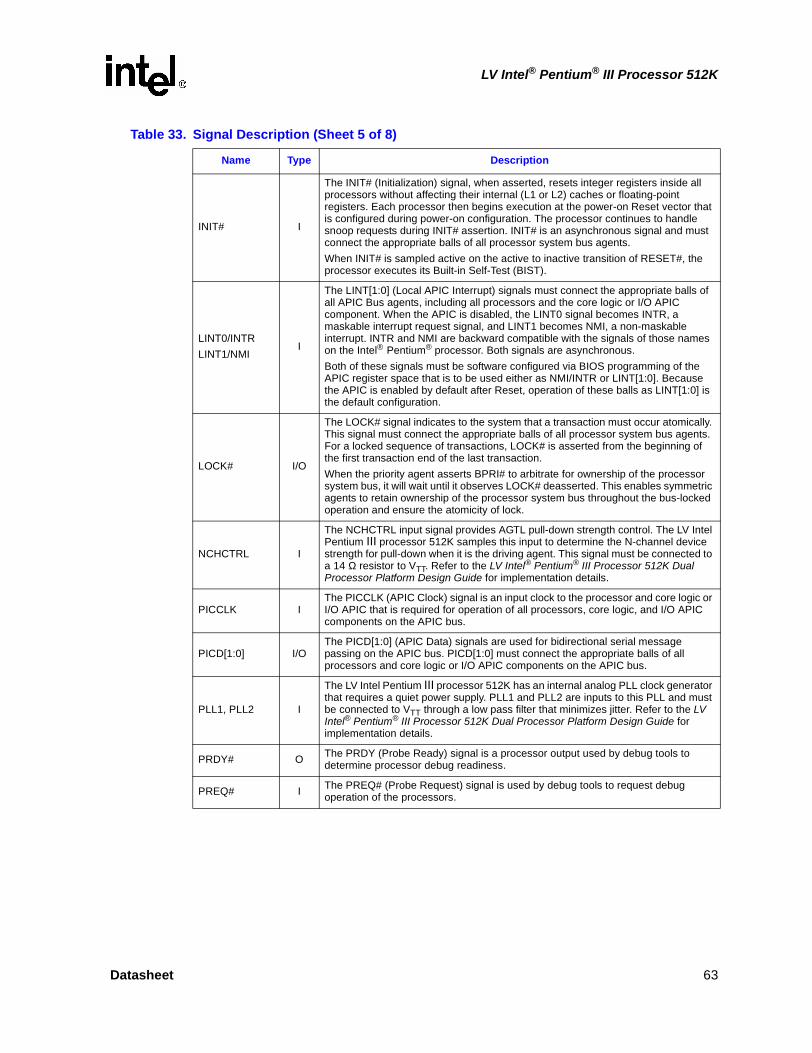
LV Intel® Pentium® III Processor 512K
INIT# I
The INIT# (Initialization) signal, when asserted, resets integer registers inside all processors without affecting their internal (L1 or L2) caches or floating-point registers. Each processor then begins execution at the power-on Reset vector that is configured during power-on configuration. The processor continues to handle snoop requests during INIT# assertion. INIT# is an asynchronous signal and must connect the appropriate balls of all processor system bus agents.When INIT# is sampled active on the active to inactive transition of RESET#, the processor executes its Built-in Self-Test (BIST).
LINT0/INTRLINT1/NMI
I
The LINT[1:0] (Local APIC Interrupt) signals must connect the appropriate balls of all APIC Bus agents, including all processors and the core logic or I/O APIC component. When the APIC is disabled, the LINT0 signal becomes INTR, a maskable interrupt request signal, and LINT1 becomes NMI, a non-maskable interrupt. INTR and NMI are backward compatible with the signals of those names on the Intel® Pentium® processor. Both signals are asynchronous.Both of these signals must be software configured via BIOS programming of the APIC register space that is to be used either as NMI/INTR or LINT[1:0]. Because the APIC is enabled by default after Reset, operation of these balls as LINT[1:0] is the default configuration.
LOCK# I/O
The LOCK# signal indicates to the system that a transaction must occur atomically. This signal must connect the appropriate balls of all processor system bus agents. For a locked sequence of transactions, LOCK# is asserted from the beginning of the first transaction end of the last transaction.When the priority agent asserts BPRI# to arbitrate for ownership of the processor system bus, it will wait until it observes LOCK# deasserted. This enables symmetric agents to retain ownership of the processor system bus throughout the bus-locked operation and ensure the atomicity of lock.
NCHCTRL I
The NCHCTRL input signal provides AGTL pull-down strength control. The LV Intel Pentium III processor 512K samples this input to determine the N-channel device strength for pull-down when it is the driving agent. This signal must be connected to a 14 Ω resistor to VTT. Refer to the LV Intel® Pentium® III Processor 512K Dual Processor Platform Design Guide for implementation details.
PICCLK IThe PICCLK (APIC Clock) signal is an input clock to the processor and core logic or I/O APIC that is required for operation of all processors, core logic, and I/O APIC components on the APIC bus.
PICD[1:0] I/OThe PICD[1:0] (APIC Data) signals are used for bidirectional serial message passing on the APIC bus. PICD[1:0] must connect the appropriate balls of all processors and core logic or I/O APIC components on the APIC bus.
PLL1, PLL2 I
The LV Intel Pentium III processor 512K has an internal analog PLL clock generator that requires a quiet power supply. PLL1 and PLL2 are inputs to this PLL and must be connected to VTT through a low pass filter that minimizes jitter. Refer to the LV Intel® Pentium® III Processor 512K Dual Processor Platform Design Guide for implementation details.
PRDY# O The PRDY (Probe Ready) signal is a processor output used by debug tools to determine processor debug readiness.
PREQ# I The PREQ# (Probe Request) signal is used by debug tools to request debug operation of the processors.
Table 33. Signal Description (Sheet 5 of 8)
Name Type Description
Datasheet 63
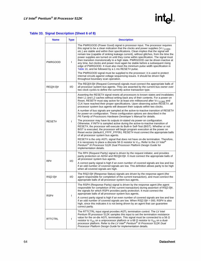
LV Intel® Pentium® III Processor 512K
PWRGOOD I
The PWRGOOD (Power Good) signal is processor input. The processor requires this signal to be a clean indication that the clocks and power supplies (VCCCORE, etc.) are stable and within their specifications. Clean implies that the signal will remain low (capable of sinking leakage current), without glitches, from the time the power supplies are turned on until they come within specification. The signal must then transition monotonically to a high state. PWRGOOD can be driven inactive at any time, but clocks and power must again be stable before a subsequent rising edge of PWRGOOD. It must also meet the minimum pulse width specification in Table 16, and be followed by a 1 ms RESET# pulse.The PWRGOOD signal must be supplied to the processor; it is used to protect internal circuits against voltage sequencing issues. It should be driven high throughout boundary scan operation.
REQ[4:0]# I/OThe REQ[4:0]# (Request Command) signals must connect the appropriate balls of all processor system bus agents. They are asserted by the current bus owner over two clock cycles to define the currently active transaction type.
RESET# I
Asserting the RESET# signal resets all processors to known states and invalidates their L1 and L2 caches without writing back any of their contents. For a power-on Reset, RESET# must stay active for at least one millisecond after VCCCORE and CLK have reached their proper specifications. Upon observing active RESET#, all processor system bus agents will deassert their outputs within two clocks.A number of bus signals are sampled at the active-to-inactive transition of RESET# for power-on configuration. These configuration options are described in the P6 Family of Processors Hardware Developer’s Manual for details.The processor may have its outputs tri-stated via power-on configuration. Otherwise, if INIT# is sampled active during the active-to-inactive transition of RESET#, the processor will execute its Built-in Self-Test (BIST). Whether or not BIST is executed, the processor will begin program execution at the power on Reset vector (default 0_FFFF_FFF0h). RESET# must connect the appropriate balls of all processor system bus agents.RESET# is the only AGTL signal that does not have on-die termination. Therefore, it is necessary to place a discrete 56 Ω resistor to VTT. Refer to the LV Intel® Pentium® III Processor 512K Dual Processor Platform Design Guide for implementation details.
RP# I/O
The RP# (Request Parity) signal is driven by the request initiator, and provides parity protection on ADS# and REQ[4:0]#. It must connect the appropriate balls of all processor system bus agents.A correct parity signal is high if an even number of covered signals are low and low if an odd number of covered signals are low. This definition allows parity to be high when all covered signals are high.
RS[2:0]# I/OThe RS[2:0]# (Response Status) signals are driven by the response agent (the agent responsible for completion of the current transaction), and must connect the appropriate balls of all processor system bus agents.
RSP# I
The RSP# (Response Parity) signal is driven by the response agent (the agent responsible for completion of the current transaction) during assertion of RS[2:0]#, the signals for which RSP# provides parity protection. It must connect the appropriate balls of all processor system bus agents.A correct parity signal is high if an even number of covered signals are low and low if an odd number of covered signals are low. When RS[2:0]# = 000, RSP# is also high, since this indicates it is not being driven by an agent that can guarantee correct parity.
RTTCTRL I
The RTTCTRL input signal provides AGTL termination control. The LV Intel Pentium III processor 512K samples this input to set the termination resistance value for the on-die AGTL termination. This signal must be connected to a 56 Ω resistor to VSS on a uniprocessor platform or a 68 Ω resistor to VSS on a dual-processor platform. Refer to the LV Intel® Pentium® III Processor 512K Dual Processor Platform Design Guide for implementation details.
Table 33. Signal Description (Sheet 6 of 8)
Name Type Description
64 Datasheet
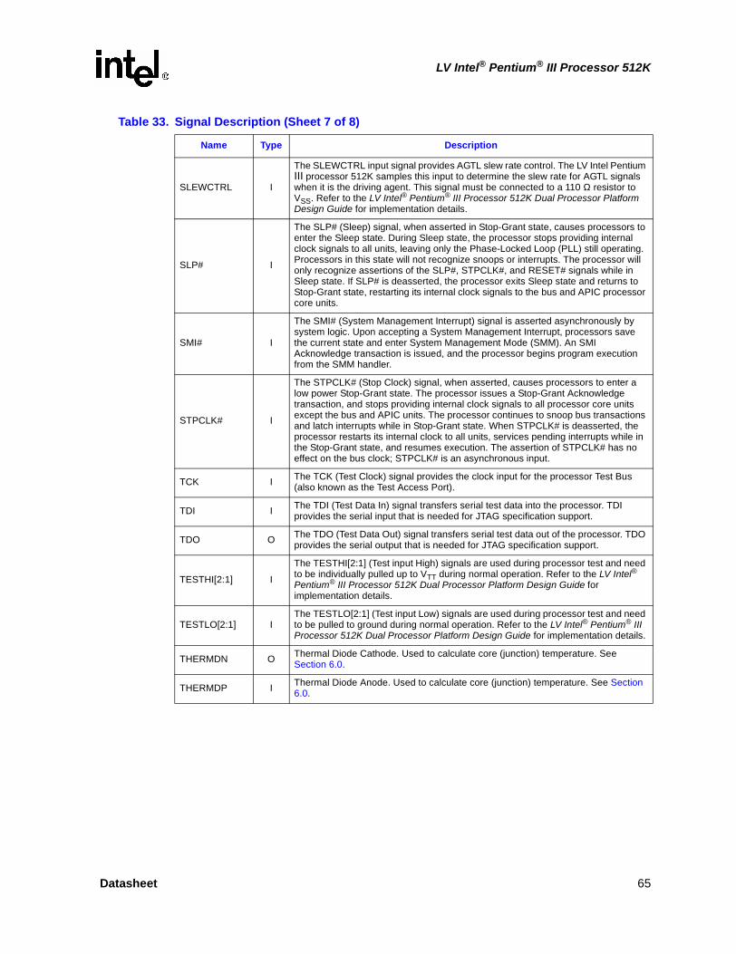
LV Intel® Pentium® III Processor 512K
SLEWCTRL I
The SLEWCTRL input signal provides AGTL slew rate control. The LV Intel Pentium III processor 512K samples this input to determine the slew rate for AGTL signals when it is the driving agent. This signal must be connected to a 110 Ω resistor to VSS. Refer to the LV Intel® Pentium® III Processor 512K Dual Processor Platform Design Guide for implementation details.
SLP# I
The SLP# (Sleep) signal, when asserted in Stop-Grant state, causes processors to enter the Sleep state. During Sleep state, the processor stops providing internal clock signals to all units, leaving only the Phase-Locked Loop (PLL) still operating. Processors in this state will not recognize snoops or interrupts. The processor will only recognize assertions of the SLP#, STPCLK#, and RESET# signals while in Sleep state. If SLP# is deasserted, the processor exits Sleep state and returns to Stop-Grant state, restarting its internal clock signals to the bus and APIC processor core units.
SMI# I
The SMI# (System Management Interrupt) signal is asserted asynchronously by system logic. Upon accepting a System Management Interrupt, processors save the current state and enter System Management Mode (SMM). An SMI Acknowledge transaction is issued, and the processor begins program execution from the SMM handler.
STPCLK# I
The STPCLK# (Stop Clock) signal, when asserted, causes processors to enter a low power Stop-Grant state. The processor issues a Stop-Grant Acknowledge transaction, and stops providing internal clock signals to all processor core units except the bus and APIC units. The processor continues to snoop bus transactions and latch interrupts while in Stop-Grant state. When STPCLK# is deasserted, the processor restarts its internal clock to all units, services pending interrupts while in the Stop-Grant state, and resumes execution. The assertion of STPCLK# has no effect on the bus clock; STPCLK# is an asynchronous input.
TCK I The TCK (Test Clock) signal provides the clock input for the processor Test Bus (also known as the Test Access Port).
TDI I The TDI (Test Data In) signal transfers serial test data into the processor. TDI provides the serial input that is needed for JTAG specification support.
TDO O The TDO (Test Data Out) signal transfers serial test data out of the processor. TDO provides the serial output that is needed for JTAG specification support.
TESTHI[2:1] I
The TESTHI[2:1] (Test input High) signals are used during processor test and need to be individually pulled up to VTT during normal operation. Refer to the LV Intel® Pentium® III Processor 512K Dual Processor Platform Design Guide for implementation details.
TESTLO[2:1] IThe TESTLO[2:1] (Test input Low) signals are used during processor test and need to be pulled to ground during normal operation. Refer to the LV Intel® Pentium® III Processor 512K Dual Processor Platform Design Guide for implementation details.
THERMDN O Thermal Diode Cathode. Used to calculate core (junction) temperature. See Section 6.0.
THERMDP I Thermal Diode Anode. Used to calculate core (junction) temperature. See Section 6.0.
Table 33. Signal Description (Sheet 7 of 8)
Name Type Description
Datasheet 65
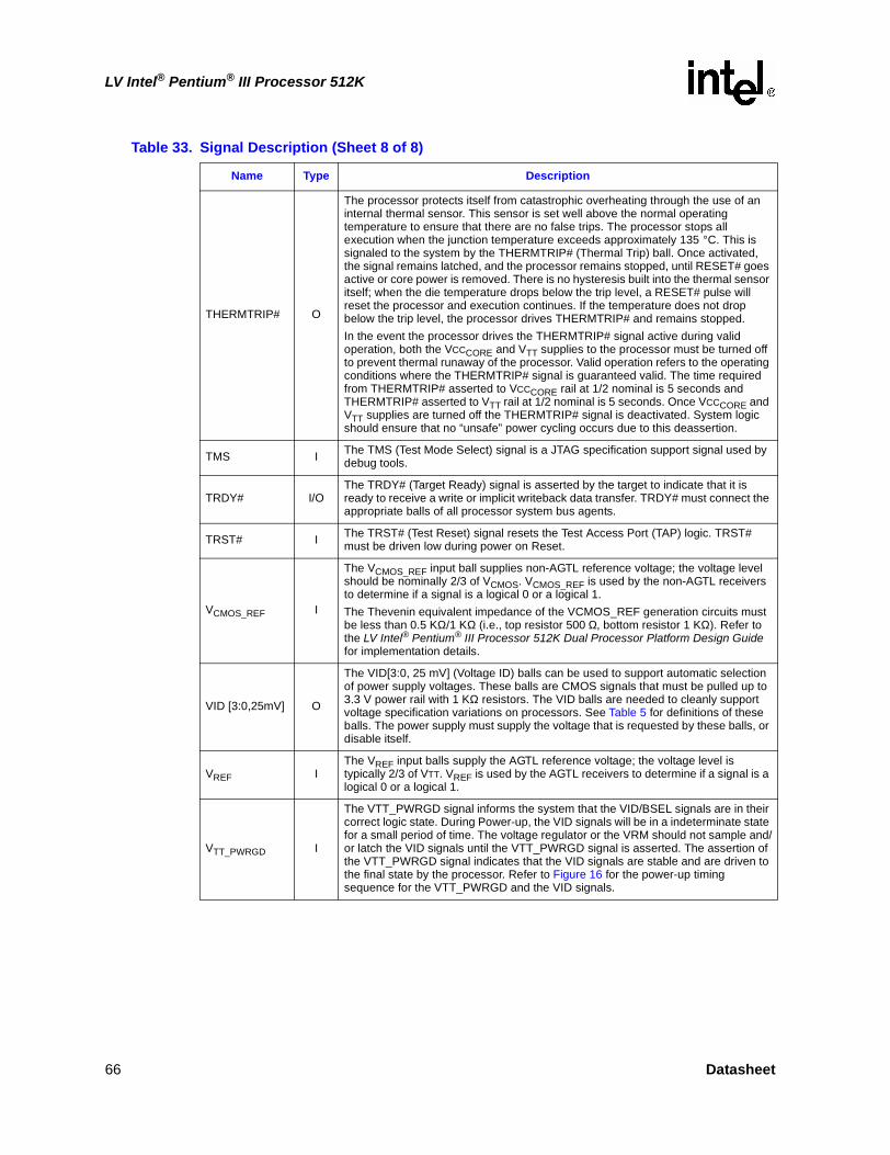
LV Intel® Pentium® III Processor 512K
THERMTRIP# O
The processor protects itself from catastrophic overheating through the use of an internal thermal sensor. This sensor is set well above the normal operating temperature to ensure that there are no false trips. The processor stops all execution when the junction temperature exceeds approximately 135 °C. This is signaled to the system by the THERMTRIP# (Thermal Trip) ball. Once activated, the signal remains latched, and the processor remains stopped, until RESET# goes active or core power is removed. There is no hysteresis built into the thermal sensor itself; when the die temperature drops below the trip level, a RESET# pulse will reset the processor and execution continues. If the temperature does not drop below the trip level, the processor drives THERMTRIP# and remains stopped.In the event the processor drives the THERMTRIP# signal active during valid operation, both the VCCCORE and VTT supplies to the processor must be turned off to prevent thermal runaway of the processor. Valid operation refers to the operating conditions where the THERMTRIP# signal is guaranteed valid. The time required from THERMTRIP# asserted to VCCCORE rail at 1/2 nominal is 5 seconds and THERMTRIP# asserted to VTT rail at 1/2 nominal is 5 seconds. Once VCCCORE and VTT supplies are turned off the THERMTRIP# signal is deactivated. System logic should ensure that no “unsafe” power cycling occurs due to this deassertion.
TMS I The TMS (Test Mode Select) signal is a JTAG specification support signal used by debug tools.
TRDY# I/OThe TRDY# (Target Ready) signal is asserted by the target to indicate that it is ready to receive a write or implicit writeback data transfer. TRDY# must connect the appropriate balls of all processor system bus agents.
TRST# I The TRST# (Test Reset) signal resets the Test Access Port (TAP) logic. TRST# must be driven low during power on Reset.
VCMOS_REF I
The VCMOS_REF input ball supplies non-AGTL reference voltage; the voltage level should be nominally 2/3 of VCMOS. VCMOS_REF is used by the non-AGTL receivers to determine if a signal is a logical 0 or a logical 1.The Thevenin equivalent impedance of the VCMOS_REF generation circuits must be less than 0.5 KΩ/1 KΩ (i.e., top resistor 500 Ω, bottom resistor 1 KΩ). Refer to the LV Intel® Pentium® III Processor 512K Dual Processor Platform Design Guide for implementation details.
VID [3:0,25mV] O
The VID[3:0, 25 mV] (Voltage ID) balls can be used to support automatic selection of power supply voltages. These balls are CMOS signals that must be pulled up to 3.3 V power rail with 1 KΩ resistors. The VID balls are needed to cleanly support voltage specification variations on processors. See Table 5 for definitions of these balls. The power supply must supply the voltage that is requested by these balls, or disable itself.
VREF IThe VREF input balls supply the AGTL reference voltage; the voltage level is typically 2/3 of VTT. VREF is used by the AGTL receivers to determine if a signal is a logical 0 or a logical 1.
VTT_PWRGD I
The VTT_PWRGD signal informs the system that the VID/BSEL signals are in their correct logic state. During Power-up, the VID signals will be in a indeterminate state for a small period of time. The voltage regulator or the VRM should not sample and/or latch the VID signals until the VTT_PWRGD signal is asserted. The assertion of the VTT_PWRGD signal indicates that the VID signals are stable and are driven to the final state by the processor. Refer to Figure 16 for the power-up timing sequence for the VTT_PWRGD and the VID signals.
Table 33. Signal Description (Sheet 8 of 8)
Name Type Description
66 Datasheet
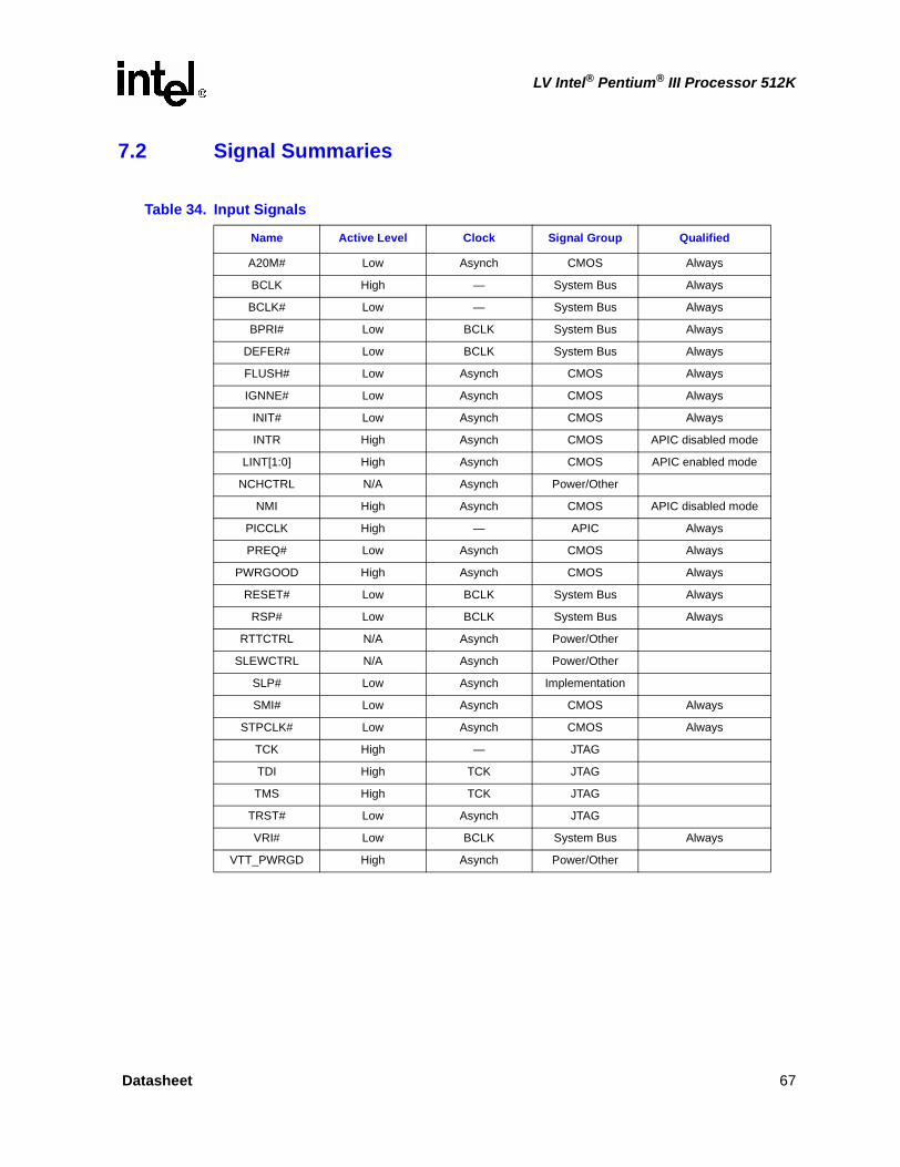
LV Intel® Pentium® III Processor 512K
7.2 Signal Summaries
Table 34. Input Signals
Name Active Level Clock Signal Group Qualified
A20M# Low Asynch CMOS Always
BCLK High — System Bus Always
BCLK# Low — System Bus Always
BPRI# Low BCLK System Bus Always
DEFER# Low BCLK System Bus Always
FLUSH# Low Asynch CMOS Always
IGNNE# Low Asynch CMOS Always
INIT# Low Asynch CMOS Always
INTR High Asynch CMOS APIC disabled mode
LINT[1:0] High Asynch CMOS APIC enabled mode
NCHCTRL N/A Asynch Power/Other
NMI High Asynch CMOS APIC disabled mode
PICCLK High — APIC Always
PREQ# Low Asynch CMOS Always
PWRGOOD High Asynch CMOS Always
RESET# Low BCLK System Bus Always
RSP# Low BCLK System Bus Always
RTTCTRL N/A Asynch Power/Other
SLEWCTRL N/A Asynch Power/Other
SLP# Low Asynch Implementation
SMI# Low Asynch CMOS Always
STPCLK# Low Asynch CMOS Always
TCK High — JTAG
TDI High TCK JTAG
TMS High TCK JTAG
TRST# Low Asynch JTAG
VRI# Low BCLK System Bus Always
VTT_PWRGD High Asynch Power/Other
Datasheet 67
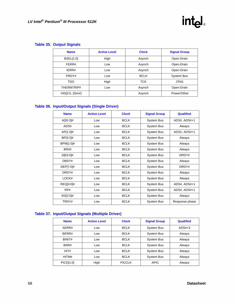
LV Intel® Pentium® III Processor 512K
Table 35. Output Signals
Name Active Level Clock Signal Group
BSEL[1:0] High Asynch Open-Drain
FERR# Low Asynch Open-Drain
IERR# Low Asynch Open-Drain
PRDY# Low BCLK System Bus
TDO High TCK JTAG
THERMTRIP# Low Asynch Open-Drain
VID[3:0, 25mV] Asynch Power/Other
Table 36. Input/Output Signals (Single Driver)
Name Active Level Clock Signal Group Qualified
A[35:3]# Low BCLK System Bus ADS#, ADS#+1
ADS# Low BCLK System Bus Always
AP[1:0]# Low BCLK System Bus ADS#, ADS#+1
BP[3:2]# Low BCLK System Bus Always
BPM[1:0]# Low BCLK System Bus Always
BR0# Low BCLK System Bus Always
D[63:0]# Low BCLK System Bus DRDY#
DBSY# Low BCLK System Bus Always
DEP[7:0]# Low BCLK System Bus DRDY#
DRDY# Low BCLK System Bus Always
LOCK# Low BCLK System Bus Always
REQ[4:0]# Low BCLK System Bus ADS#, ADS#+1
RP# Low BCLK System Bus ADS#, ADS#+1
RS[2:0]# Low BCLK System Bus Always
TRDY# Low BCLK System Bus Response phase
Table 37. Input/Output Signals (Multiple Driver)
Name Active Level Clock Signal Group Qualified
AERR# Low BCLK System Bus ADS#+3
BERR# Low BCLK System Bus Always
BINIT# Low BCLK System Bus Always
BNR# Low BCLK System Bus Always
HIT# Low BCLK System Bus Always
HITM# Low BCLK System Bus Always
PICD[1:0] High PICCLK APIC Always
68 Datasheet
Contents
1 Related Documents ......................................................................................................................92 LV/ULV Intel® Pentium® III Processor 512K CPUID .................................................................153 System Bus Signal Groups.........................................................................................................164 BSEL[1:0] Encoding....................................................................................................................175 LV Intel Pentium III Processor 512K VID Values ........................................................................226 LV Intel Pentium III Processor 512K Absolute Maximum Ratings ..............................................247 Power Specifications for LV Intel Pentium III Processor 512K ...................................................258 VccCORE Static and Transient Tolerance ...................................................................................279 AGTL Signal Group Levels Specifications..................................................................................2810 Processor AGTL Bus Specifications...........................................................................................2811 CLKREF, APIC, TAP, CMOS, and Open-Drain Signal Group DC Specifications ......................2912 System Bus Clock AC Specifications (Differential).....................................................................3013 System Bus Clock AC Specifications (133 MHz, Single-Ended) ................................................3114 Valid LV Intel Pentium III Processor 512K Frequencies .............................................................3215 AGTL Signal Groups AC Specifications .....................................................................................3216 CMOS and Open-Drain Signal Groups AC Specifications .........................................................3217 Reset Configuration AC Specifications and Power On Timings .................................................3318 APIC Bus Signal AC Specifications ............................................................................................3319 TAP Signal AC Specifications.....................................................................................................3420 BCLK (Differential) DC Specifications and AC Signal Quality Specifications .............................4021 BCLK (Single-Ended) DC Specifications and AC Signal Quality Specifications.........................4022 PICCLK DC Specifications and AC Signal Quality Specifications ..............................................4123 133 MHz AGTL Signal Group Overshoot/Undershoot Tolerance
at the Processor Core.................................................................................................................4324 Non-AGTL Signal Group Overshoot/Undershoot Tolerance at the Processor Core ..................4325 Micro-FCBGA Package Mechanical Specifications ....................................................................4626 Signal List by Ball Number..........................................................................................................5127 Signal Listing by Signal Name....................................................................................................5428 Voltage and No-Connect Ball Locations .....................................................................................5629 LV Intel Pentium III Processor 512K Thermal Design Power .....................................................5730 THERMTRIP# Time Requirement ..............................................................................................5731 Thermal Diode Interface .............................................................................................................5832 Thermal Diode Parameters.........................................................................................................5833 Signal Description.......................................................................................................................5934 Input Signals ...............................................................................................................................6735 Output Signals ............................................................................................................................6836 Input/Output Signals (Single Driver) ...........................................................................................6837 Input/Output Signals (Multiple Driver).........................................................................................68
Datasheet 1

Contents
2 Datasheet
Contents
1 AGTL Bus Topology ...................................................................................................................112 Stop Clock State Machine ..........................................................................................................123 Differential/Single-Ended Clocking Example ..............................................................................154 Single Ended Clock BSEL Circuit (133 MHz) .............................................................................185 Differential Clock BSEL Circuit ...................................................................................................196 PLL Filter ....................................................................................................................................217 VTT Power Good and Bus Select Interconnect Diagram ............................................................238 Power Supply Current Slew Rate (dIccCORE/dt) .........................................................................269 VccCORE Static and Transient Tolerance ...................................................................................2710 BCLK (Single Ended)/PICCLK/TCK Generic Clock Timing Waveform.......................................3511 Differential BCLK/BCLK# Waveform (Common Mode) ..............................................................3512 BCLK/BCLK# Waveform (Differential Mode) ..............................................................................3613 Valid Delay Timings....................................................................................................................3614 Setup and Hold Timings .............................................................................................................3715 Cold/Warm Reset and Configuration Timings ............................................................................3716 Power-On Sequence and Reset Timings ...................................................................................3817 Test Timings (Boundary Scan) ...................................................................................................3918 Test Reset Timings.....................................................................................................................3919 BCLK (Single-Ended)/PICCLK Generic Clock Waveform ..........................................................4120 Maximum Acceptable Overshoot/Undershoot Waveform...........................................................4221 Noise Estimation.........................................................................................................................4522 Micro-FCBGA Package – Top and Bottom Isometric Views.......................................................4723 Micro-FCBGA Package – Top and Side Views ..........................................................................4824 Micro-FCBGA Package - Bottom View.......................................................................................4925 Ball Map - Top View....................................................................................................................50
Datasheet 1

Contents
2 Datasheet
Contents
1.0 Introduction....................................................................................................................................71.1 Overview...............................................................................................................................71.2 Terminology ..........................................................................................................................81.3 Related Documents ..............................................................................................................9
2.0 Processor Features .....................................................................................................................102.1 512-Kbyte On-Die Integrated L2 Cache .............................................................................102.2 Data Prefetch Logic ............................................................................................................102.3 Processor System Bus and VREF.............................................................................................................. 102.4 Differential Clocking............................................................................................................112.5 Clock Control and Low Power States .................................................................................11
2.5.1 Normal State—State 1...........................................................................................122.5.2 AutoHALT Power Down State—State 2 ................................................................122.5.3 Stop-Grant State—State 3.....................................................................................132.5.4 HALT/Grant Snoop State—State 4........................................................................132.5.5 Sleep State—State 5 .............................................................................................132.5.6 Clock Control .........................................................................................................14
2.6 Power and Ground Balls.....................................................................................................142.7 Processor System Bus Clock and Processor Clocking ......................................................142.8 Processor System Bus Unused Balls .................................................................................152.9 LV Intel Pentium III Processor 512K CPUID.......................................................................15
3.0 Electrical Specifications .............................................................................................................163.1 Processor System Bus Signal Groups................................................................................16
3.1.1 Asynchronous vs. Synchronous for System Bus Signals ......................................173.1.2 System Bus Frequency Select Signals ..................................................................17
3.2 Single-Ended Clocking BSEL[1:0] Implementation.............................................................173.3 Differential Host Bus Clocking Routing...............................................................................18
3.3.1 Differential Clocking BSEL[1:0] Implementation ....................................................183.4 Signal State in Low-Power States ......................................................................................19
3.4.1 System Bus Signals ...............................................................................................193.4.2 CMOS and Open-Drain Signals.............................................................................193.4.3 Other Signals .........................................................................................................19
3.5 Test Access Port (TAP) Connection ...................................................................................203.6 Power Supply Requirements ..............................................................................................20
3.6.1 Decoupling Guidelines...........................................................................................203.6.2 Processor VCCCORE Decoupling ...........................................................................203.6.3 Voltage Planes.......................................................................................................21
3.7 Voltage Identification ..........................................................................................................213.8 System Bus Clock and Processor Clocking........................................................................243.9 Maximum Ratings ...............................................................................................................243.10 DC Specifications ...............................................................................................................253.11 AC Specifications................................................................................................................30
3.11.1 System Bus, Clock, APIC, TAP, CMOS, and Open-Drain AC Specifications........30
4.0 System Signal Simulations.........................................................................................................404.1 System Bus Clock (BCLK) and PICCLK DC
Specifications and AC Signal Quality Specifications ..........................................................404.2 AGTL AC Signal Quality Specifications ..............................................................................424.3 Non-AGTL Signal Quality Specifications ............................................................................43
Datasheet 1
Contents
4.3.1 PWRGOOD Signal Quality Specification............................................................... 444.3.2 VTT_PWRGD Signal Quality Specification............................................................44
5.0 Mechanical Specifications.......................................................................................................... 465.1 Surface Mount Micro-FCBGA Package .............................................................................. 465.2 Signal Listings..................................................................................................................... 50
6.0 Thermal Specifications and Design Considerations................................................................ 576.1 Thermal Specifications ....................................................................................................... 57
6.1.1 THERMTRIP# Requirement .................................................................................. 576.1.2 Thermal Diode ....................................................................................................... 58
7.0 Processor Interface ..................................................................................................................... 597.1 Alphabetical Signals Reference.......................................................................................... 597.2 Signal Summaries............................................................................................................... 67
2 Datasheet