Embed Size (px)
Citation preview
Low Variability in Synthetic Monolayer MoS2DevicesKirby K. H. Smithe,† Saurabh V. Suryavanshi,† Miguel Munoz Rojo,† Aria D. Tedjarati,†
and Eric Pop*,†,‡,§
†Department of Electrical Engineering, ‡Department of Materials Science and Engineering, and §Precourt Institute for Energy,Stanford University, Stanford, California 94305, United States
*S Supporting Information
ABSTRACT: Despite much interest in applications of two-dimensional (2D) fabrics such as MoS2, to date most studieshave focused on single or few devices. Here we examine thevariability of hundreds of transistors from monolayer MoS2synthesized by chemical vapor deposition. Ultracleanfabrication yields low surface roughness of ∼3 Å andsurprisingly low variability of key device parameters,considering the atomically thin nature of the material.Threshold voltage variation and very low hysteresis suggestvariations in charge density and traps as low as ∼1011 cm−2.Three extraction methods (field-effect, Y-function, andeffective mobility) independently reveal mobility from 30 to 45 cm2/V/s (10th to 90th percentile; highest value ∼48cm2/V/s) across areas >1 cm2. Electrical properties are remarkably immune to the presence of bilayer regions, which causeonly small conduction band offsets (∼55 meV) measured by scanning Kelvin probe microscopy, an order of magnitudelower than energy variations in Si films of comparable thickness. Data are also used as inputs to Monte Carlo circuitsimulations to understand the effects of material variability on circuit variation. These advances address key missing stepsrequired to scale 2D semiconductors into functional systems.
KEYWORDS: MoS2, chemical vapor deposition, variability, mobility, threshold voltage, band offsets
As the study of two-dimensional (2D) materialscontinues into its second decade, functionality beyondindividual devices is gaining importance and being
explored in the form of simple circuits implemented ingraphene1−3 and transition-metal dichalcogenides (TMDs).4,5
Further implementation of realistic systems based on 2Dsemiconductor TMDs must rely on large-area films grown, e.g.,by chemical vapor deposition (CVD). Recent studies haveshown steady and increasing improvement in metrics such asmobility and contact resistance for CVD-grown MoS2,
6,7
facilitated in part by recent progress in transfer8−10 and CVDprocesses.11−15 However, CVD-grown monolayer (1L) semi-conductors present distinctive sources of variability, such ascrystal orientation, grain boundaries, and small islands of bilayer(2L) regions. Only a few TMD studies have looked beyondindividual devices,16,17 and a thorough investigation intointrinsic material variability, its physical origins, and how itwill affect system performance is presently lacking.Herein we explore this variability for important metrics such
as threshold voltage (VT), charge trap density (nt), currentmax/min ratio, mobility, and hysteresis (H) of hundreds oftransistors fabricated from >1 cm2 areas of CVD-grownmonolayer MoS2 films. These 2D fabrics achieve metrics (e.g.,low hysteresis, high mobility) on par with or better than other
CVD-grown films reported to date. In addition, we find that theelectrical effects of TMD thickness variation (e.g., 1L to 2L) arean order of magnitude less severe than would be expected forsilicon films of comparable thickness. We also use our data asinputs for Monte Carlo simulations of standard logic cells andanalyze the effect that intrinsic material variability has on keysystem properties, including energy consumption and delay.Such insight into the variability of 2D semiconductors is crucialfor future applications, and for comparison to technologies suchas ultrathin body silicon-on-insulator (UTB SOI) or oxidesemiconductors which could potentially be replaced orcomplemented by TMDs.18−21
RESULTS AND DISCUSSION
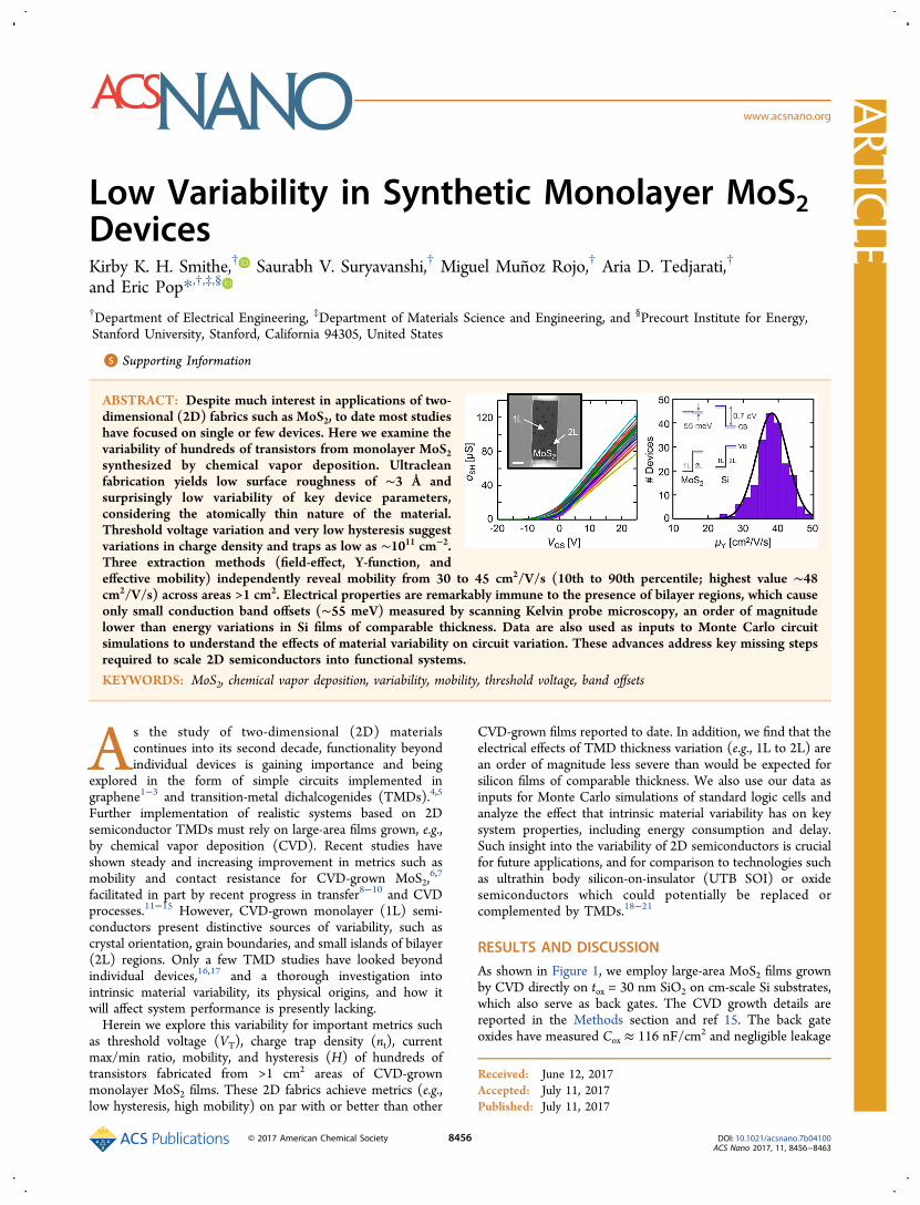
As shown in Figure 1, we employ large-area MoS2 films grownby CVD directly on tox = 30 nm SiO2 on cm-scale Si substrates,which also serve as back gates. The CVD growth details arereported in the Methods section and ref 15. The back gateoxides have measured Cox ≈ 116 nF/cm2 and negligible leakage
Received: June 12, 2017Accepted: July 11, 2017Published: July 11, 2017
Artic
lewww.acsnano.org
© 2017 American Chemical Society 8456 DOI: 10.1021/acsnano.7b04100ACS Nano 2017, 11, 8456−8463
up to 25 V (see Supporting Information Figure S1). The cm2
MoS2 films are continuous large-grain 1L with a small fractionbeing bilayer (2L) regions, as shown in Figure 1a,b. Opticallithography is used to fabricate hundreds of field-effecttransistors (FETs) of varying length and width (L and W) ona single chip, as seen in Figure 1c, and fabrication details areprovided in the Methods section and Supporting Informationsection B. A top-view scanning electron microscope (SEM)image and a cartoon of the device geometry are shown inFigure 1d,e, respectively. Small 2L regions (≤0.5 μm2) arevisible in the channel, which is itself a single 1L crystal, as thegrain size of these films is ∼100 μm.Electrical Measurements. Direct current (DC) electrical
characteristics of 200 devices were measured to give statisticaldata for threshold voltage VT, density of charge traps nt,hysteresis H, Imax/Imin current ratio, and three definitions ofmobility: field-effect μFE, Y-function μY, and effective mobilityμeff (see Methods). Such data consist primarily of forward−backward ID−VGS sweeps (at VDS = 0.1 and 1.0 V), as shown inFigure 1f. VT was extracted using four methods from the ID−VGS sweeps:22,23 linear extrapolation, constant-current (CC),(ID)
1/2, and Y-function methods. Only the well-known linearextrapolation method is analyzed in depth here, as its variationdirectly corresponds to variation in charge density. An upperbound of nt = ΔVTCox/q is estimated conservatively by findingthe difference ΔVT between forward and backward sweeps,24
where q is the elementary charge. The ratio of maximum tominimum current is Imax/Imin, employed here because the “on/off ratio” is not well-defined without given voltage rails in acircuit (see Supporting Information Figure S5). The μFE isproportional to the maximum transconductance (gm = ∂ID/∂VGS), as μFE = gmL(WCoxVDS)
−1. H is the maximum measureddifference in constant-current voltage from the forward andbackward sweeps across the entire linear portion of the curve(note that it is very small for our devices). We also quantify W
and L, the fabricated device widths and lengths as measured bySEM (summarized in Supporting Information Figure S7).For all 200 devices, we calculate the mean and standard
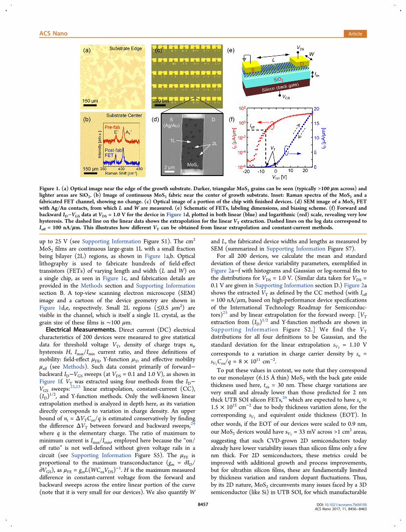
deviation of these device variability parameters, exemplified inFigure 2a−f with histograms and Gaussian or log-normal fits tothe distributions for VDS = 1.0 V. (Similar data taken for VDS =0.1 V are given in Supporting Information section D.) Figure 2ashows the extracted VT as defined by the CC method (with Ioff= 100 nA/μm, based on high-performance device specificationsof the International Technology Roadmap for Semiconduc-tors)25 and by linear extrapolation for the forward sweep. [VT
extraction from (ID)1/2 and Y-function methods are shown in
Supporting Information Figure S2.] We find the VT
distributions for all four definitions to be Gaussian, and thestandard deviation for the linear extrapolation sVT
= 1.10 Vcorresponds to a variation in charge carrier density by sn =sVTCox/q = 8 × 1011 cm−2.To put these values in context, we note that they correspond
to our monolayer (6.15 Å thin) MoS2 with the back gate oxidethickness used here, tox = 30 nm. These charge variations arevery small and already lower than those predicted for 2 nmthick UTB SOI silicon FETs,26 which are expected to have sn ≈1.5 × 1012 cm−2 due to body thickness variation alone, for thecorresponding sVT
and equivalent oxide thickness (EOT). Inother words, if the EOT of our devices were scaled to 0.9 nm,our MoS2 devices would have sVT
= 33 mV across >1 cm2 areas,suggesting that such CVD-grown 2D semiconductors todayalready have lower variability issues than silicon films only a fewnm thick. For 2D semiconductors, these metrics could beimproved with additional growth and process improvements,but for ultrathin silicon films, these are fundamentally limitedby thickness variation and random dopant fluctuations. Thus,by its 2D nature, MoS2 circumvents many issues faced by a 3Dsemiconductor (like Si) in UTB SOI, for which manufacturable
Figure 1. (a) Optical image near the edge of the growth substrate. Darker, triangular MoS2 grains can be seen (typically >100 μm across) andlighter areas are SiO2. (b) Image of continuous MoS2 fabric near the center of growth substrate. Inset: Raman spectra of the MoS2 and afabricated FET channel, showing no change. (c) Optical image of a portion of the chip with finished devices. (d) SEM image of a MoS2 FETwith Ag/Au contacts, from which L and W are measured. (e) Schematic of FETs, labeling dimensions, and biasing scheme. (f) Forward andbackward ID−VGS data at VDS = 1.0 V for the device in Figure 1d, plotted in both linear (blue) and logarithmic (red) scale, revealing very lowhysteresis. The dashed line on the linear data shows the extrapolation for the linear VT extraction. Dashed lines on the log data correspond toIoff = 100 nA/μm. This illustrates how different VT can be obtained from linear extrapolation and constant-current methods.
ACS Nano Article
DOI: 10.1021/acsnano.7b04100ACS Nano 2017, 11, 8456−8463
8457
solutions are not currently known beyond the 5 nm technologynode.ΔVT for our devices is also Gaussian, with a mean value of
⟨ΔVT⟩ = 0.16 V, corresponding to nt = 1.1 × 1011 cm−2, assummarized in Figure 2b. This value implies that lowerdensities of charge traps are present in high-quality CVD-grownMoS2 (and at the SiO2 interface) than previously suggested forsome exfoliated samples.27,28 A further indication of chargetrapping is the measured constant-current hysteresis H,29 whichwe find to have a mean and standard deviation ⟨H⟩ = 0.14 Vand sH = 0.07 V (Figure 2c), indicating that our devices arelargely independent of their own bias history for electric fieldsup to 0.25 V/μm laterally and 1 V/nm vertically. For the decileof devices with the lowest hysteresis, these 20 all demonstratedH ≤ 50 mV. While these values are obtained for tox = 30 nm,scaling to an EOT = 0.9 nm would give a very small average⟨H⟩ ≈ 4.2 mV, as shown along the top horizontal axis of Figure2c. This is much smaller than the supply voltages of moderncircuits, and thus large-scale implementation of CVD-grownMoS2 is already not hindered by intrinsic variability today,provided the EOT is scaled accordingly.Figure 2d reveals that the measured Imax/Imin ratio follows a
log-normal distribution. This is unsurprising given that sVTis
normally distributed and the subthreshold current Isub ∝exp(VGS − VT).
30 For our devices, the median measured Imax/Imin = 5.3 × 10⁶ A/A, keeping in mind that actual current ratioscould be higher, as Imin can be limited by the measurementnoise floor (∼ pA here, as seen in Figure 1f). Additionalvisualizations of these data and the rest that follow are availablein the Supporting Information sections C and D, in the form ofcumulative distribution functions and box-and-whisker plots.In order to decouple the measured electrical variation from
geometric variation, all devices were measured by SEM toobtain precise values for L and W. Figure 2e shows the field-effect mobility distribution, with mean ⟨μFE⟩ = 34.2 cm2/V/sand standard deviation sμFE = 3.6 cm2/V/s, which yields a
coefficient of variation CVμ = sμ/⟨μFE⟩ = 0.10. W and L, on theother hand (Supporting Information Figure S7), weremeasured to have CVW = 0.01 and CVL = 0.05. This impliesthat, given nominal values of L and W, the CV for nominal μFEbased on what the dimensions of the devices should be (ratherthan what they actually are) is31 (CVL
2 + CVW2 + CVμ
2)1/2 =0.12. In other words, variations in lithographic features here aresufficiently small that the device behavior has a variation only2% larger when assuming L andW are their average values fromlithography. Indeed, this is exactly what we observe: Whenassuming that L and W are their average values and repeatingthe analysis, ⟨μFE⟩ remains 34.2 cm2/V/s while the standarddeviation sμFE slightly increases to 4.1 cm2/V/s, resulting in CV= 0.12 (see Supporting Information Figure S8).To further analyze mobility, we employ the Y-function
method, (see ref 23 and Supporting Information section E),whereby we calculate μY = 38.2 ± 8.8 cm2/V/s and RCY = 3.0 ±1.4 kΩ·μm (see Figure 2f and Supporting Information FigureS9), where the uncertainties here are indicative of two standarddeviations (95% inclusive). We note that this estimation ofcontact resistance is an upper bound and that the true RC couldbe lower. The 10th to 90th percentile of mobilities extracted bythe field-effect and Y-function methods ranges from 30 to 45cm2/V/s (highest value ∼48 cm2/V/s from the Y-functionapproach). Additionally, we note that the mobility extractedfrom the Y-function approach is slightly higher than the othermethods because the Y-function typically gives a higher VT thanthe linear extrapolation method.32
Linear and log-scale data for the sheet conductance [σSH =IDL/(VDSW)] of an example 30 of our devices are plotted inFigure 3a and its inset, respectively, at VDS = 0.1 V. These typesof measurements across the entire data set were used forpseudo-transfer length method (pTLM) analysis. Unlike thelinear TLM, where resistances of several channel lengths aremeasured along the same material strip with shared contacts,33
for the pTLM we measure resistances (RTOT) of all our devices
Figure 2. Histograms and distribution fits of statistical data. (a) VT for both the linear extrapolation (blue) and constant-current (Ioff = 100nA/μm, red) methods. (b) nt as estimated from ΔVT. (c) Hysteresis in forward−backward ID−VGS sweeps, which we observe to follow a log-normal distribution. Top horizontal axis shows the very small hysteresis expected if the EOT is scaled to 0.9 nm. (d) Imax/Imin is also log-normal, since subthreshold current is exponentially dependent on VT. (e and f) Histogram of mobility values as extracted from (e) the field-effect and (f) the Y-function approach. Note that μY > μFE in all cases due to the differences in extractions methods.
ACS Nano Article
DOI: 10.1021/acsnano.7b04100ACS Nano 2017, 11, 8456−8463
8458

with various L and W distributed across the chip, constructingthe scatter plot in Figure 3b. We fit the linear regression lines tothe 10th through 90th percentiles of devices, noting that RTOTdistributions are Gaussian with respect to L andW. The verticalintercept of the pTLM line fits is twice the contact resistance,and the slope is the sheet resistance, which can be used toestimate the effective mobility. In Figure 3c this analysis yieldsvalues for μeff = 33.8 ± 2.8 cm2/V/s and RC = 1.0 ± 2.6 kΩ·μmat n = 1.8 × 1013 cm−2, where the uncertainties reflect 95%confidence intervals in the fitting. We note that despite theuncertainty of contact resistance in the pTLM method, therange of RC reported in this work for all extraction methods isamong the best reported today for monolayer, undoped MoS2.We attribute these results to the cleanliness of our processconditions and the use of Ag/Au contacts deposited inultrahigh vacuum (see Supporting Information Section B).It is important to emphasize that all figures of merit discussed
here are for monolayer, CVD-grown MoS2, a sub-1 nm thinsemiconductor. In contrast, silicon has an effective mobility of∼2 cm2/V/s for comparable thickness and carrier densities34
due to strong surface roughness scattering and atomic-scalethickness fluctuations. However, it is evident even from micron-scale devices that improvements in contact engineering arecurrently the greatest issue facing the scaling of TMD systemsfrom a device perspective. The contact resistance achieved hereon a large scale is of the order 1.0 kΩ·μm for n ≥ 1013 cm−2,among the best reported for a monolayer semiconductorwithout deliberate doping. This must be further lowered by upto an order of magnitude, as devices <100 nm would be ∼50%contact dominated with similar contacts.33
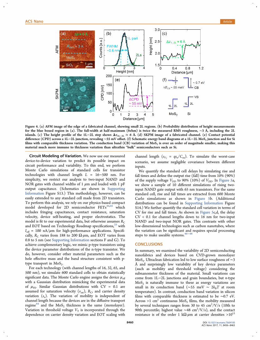
Surface Imaging and Analysis. To gain physical insightinto why our MoS2 devices show relatively low variation giventhe atomically thin nature of this material, we performmeasurements including atomic force microscopy (AFM),scanning Kelvin probe microscopy (SKPM), and SEM analysisof grain boundaries on the fabricated devices. The surfaceroughness of our MoS2 FETs is quantified via AFM includingthe 2L regions as shown in Figure 4a, and the root-mean-square(RMS) value is only 3 Å (Figure 4b) af ter fabrication, which isnear the limit of AFM capabilities and comparable to similarmeasurements on freshly exfoliated MoS2 on SiO2.
35 Weattribute this low roughness as well as the negligible hysteresisand low variability of our devices in part to our growth andprocessing methods (Supporting Information section B), which
yield devices remarkably free of cracks, wrinkles, or photoresistresidue. The small tail at the upper end of the curve in Figure4b is due to the 2L regions, and the distribution does notchange if sampling over the entire FET channel. Figure 4cshows the 1L−2L junction step height measured by AFM isΔz1L−2L ≈ 6 Å, in agreement with the two Gaussian fits inFigure 4b as well as the 6.15 Å MoS2 layer separation observedby neutron diffraction studies on bulk samples.36
SKPM imaging in Figure 4d,e reveals the contact potentialdifference (CPD) at 1L−2L boundaries is only ∼55 meV,confirming recent studies which have shown that 1L−2L MoS2conduction band (CB) offsets are relatively small, ΔECB ∼ 2kBTat room temperature.37,38 The surface potential “jumps” at the2L edges are due to the higher reactivity of the edges,39,40
ostensibly from adsorbates accumulated during long SKPMmeasurements in air. To compare these findings with variabilityin ultrathin silicon, we turn to Figure 4f. This illustrates thatΔECB in MoS2 is over an order of magnitude smaller than CBoffsets calculated for comparable thickness variation (1L vs 2L)in Si, which are ∼0.7 eV depending on crystal orientation.41,42
Thus, in addition to robustness against short-channel effects inultrathin body transistors, 1L MoS2 films also offer naturalrobustness to fluctuations in VT and on-state electron densitycaused by thickness irregularities. For n-type applications theCB variation is nearly negligible at room temperature, since themajority of the potential discontinuity occurs in the valenceband of MoS2.
37 Other monolayer semiconductors will need tobe similarly evaluated for variation (or lack thereof) in p-typeapplications.SEM images of our fabricated FETs (such as Figure 1d) also
reveal that, out of 200 channels with ∼10 μm2 area, 116 aresingle-crystal, 75 have a single grain boundary (GB), and 9 havetwo GBs. However, the presence of GBs does not appear toaffect device performance to a significant degree, consistentwith previous results.43 Similar to 1L−2L junctions, Huang etal. (ref 37) found that CB offsets at GBs are also small andmost energy discontinuities occur in the valence band. Notethat all our measured device variability includes randomdistributions of 2L islands and ∼40% of our devices have atleast one GB. We do not observe bi- or trimodal distributionsin our data and thus conclude (supported by our and others’surface analysis) that the electrical variability introduced bysmall 2L regions and GBs is minimal for n-type monolayerMoS2 nanofabrics operating at room temperature.
Figure 3. (a) Sheet conductance σSH vs VGS for a representative sample of 30 devices. The inset shows the same data displayed in log scale. TheVT variation seen here corresponds to a subset of that recorded in Figure 2a. The EOT here is 30 nm, however if this were scaled to 0.9 nm,these MoS2 devices would have sVT
= 33 mV across >1 cm2 areas (see text). (b) Pseudo-TLM (pTLM) analysis showing measured RTOT vs L(symbols) for the 10th through 90th percentile of devices at n = 4 to 18 × 1012 cm−2, with linear regression fits. The color gradient marks theincreasing carrier density. The slope of the linear fits corresponds to the sheet resistance RSH = (qnμeff)
−1, and the abscissa intercept is 2RC. (c)RC vs n as extracted from the pTLM, with error bars reflecting 95% confidence intervals and a minimum of 730 Ω·μm at n ≈ 1.3 × 1013 cm−2.Inset: Effective mobility μeff vs n for the same fitting, reaching ∼34 cm2/V/s for all n ≥ 4 × 1012 cm−2.
ACS Nano Article
DOI: 10.1021/acsnano.7b04100ACS Nano 2017, 11, 8456−8463
8459
Circuit Modeling of Variation. We now use our measureddevice-to-device variation to predict its possible impact oncircuit performance and variability. To this end, we performMonte Carlo simulations of standard cells for transistortechnologies with channel length L = 16−500 nm. Forsimplicity, we restrict our analysis to two-input NAND andNOR gates with channel widths of 1 μm and loaded with 1 pFoutput capacitance. (Schematics are shown in SupportingInformation Figure S13.) This methodology, however, can beeasily extended to any standard cell made from 2D transistors.To perform this analysis, we rely on our physics-based compactmodel developed for 2D semiconductor FETs44,45 whichincludes fringing capacitances, contact resistance, saturationvelocity, device self-heating, and proper electrostatics. Themodel is fit to our experimental data, but otherwise assumes RCand EOT based on Technology Roadmap specifications,25 withIoff = 100 nA/μm for high-performance applications. Specifi-cally, RC varies from 188 to 200 Ω·μm, and EOT varies from0.8 to 5 nm (see Supporting Information sections F and G). Toachieve complementary logic, we mimic p-type transistors usingthe device parameter distributions of the n-type transistor. Wedo, however, consider other material parameters such as thehole effective mass and the band structure consistent with p-type transport in MoS2.For each technology (with channel lengths of 16, 32, 65, and
500 nm), we simulate 600 standard cells to obtain statisticallysignificant data. The Monte Carlo engine assigns the device μeffwith a Gaussian distribution mimicking the experimental dataof μFE. Similar Gaussian distributions with CV = 0.1 areassumed for saturation velocity (vsat), RC, and carrier densityvariation (sn). The variation of mobility is independent ofchannel length because the devices are in the diffusive transportregime44 and the MoS2 thickness is the same (monolayer).Variation in threshold voltage VT is incorporated through thedependence on carrier density variation and EOT scaling with
channel length (sVT= qsn/Cox). To simulate the worst-case
scenario, we assume negligible covariance between differentinputs.We quantify the standard cell delays by simulating rise and
fall times and define the output rise (fall) time from 10% (90%)of the supply voltage VDD to 90% (10%) of VDD. In Figure 5a,we show a sample of 10 different simulations of rising two-input NAND gate output with 65 nm transistors. For the samestandard cell, rise and fall times are extracted from 600 MonteCarlo simulations as shown in Figure 5b. (Additionaldistributions can be found in Supporting Information FigureS14.) We further quantify the standard cell variation in terms ofCV for rise and fall times. As shown in Figure 5c,d, the delayCV < 0.1 for channel lengths down to 16 nm for two-inputNAND and two-input NOR gates. This contrasts with otherlow-dimensional technologies such as carbon nanotubes, wherethe variation can be significant and requires special processingsteps to make useable systems.46−48
CONCLUSIONSIn summary, we examined the variability of 2D semiconductingnanofabrics and devices based on CVD-grown monolayerMoS2. Ultraclean fabrication led to low surface roughness of ∼3Å and surprisingly low variability of key device parameters(such as mobility and threshold voltage) considering thesubnanometer thickness of the material. Small variations cancome from 1L−2L junctions and grain boundaries, but n-typeMoS2 is naturally immune to these as energy variations aresmall in its conduction band (∼55 meV ∼ 2kBT at roomtemperature). In contrast, conduction band variation in siliconfilms with comparable thickness is estimated to be ∼0.7 eV.Across >1 cm2 continuous MoS2 films, the mobility measuredby several techniques ranges from 30 to 45 cm2/V/s (10th to90th percentile; highest value ∼48 cm2/V/s), and the contactresistance is of the order 1 kΩ·μm at carrier densities >1013
Figure 4. (a) AFM image of the edge of a fabricated channel, showing small 2L regions. (b) Probability distribution of height measurementsfor the blue boxed region in (a). The full-width at half-maximum (fwhm) is twice the measured RMS roughness, ∼3 Å, including the 2Lislands. (c) The height profile of the 1L−2L step shows Δz1L−2L ≈ 6 Å. (d) SKPM image of a fabricated channel. (e) Contact potentialdifference (CPD) across a 1L−2L junction, revealing ∼55 mV offset. (f) Schematic energy band diagrams at a 1L−2L MoS2 junction and for Sifilms with comparable thickness variation. The conduction band (CB) variation of MoS2 is over an order of magnitude smaller, making thismaterial much more immune to thickness variation than ultrathin “bulk” semiconductors such as Si.
ACS Nano Article
DOI: 10.1021/acsnano.7b04100ACS Nano 2017, 11, 8456−8463
8460

cm−2. These values are among the best obtained to date forundoped monolayer CVD-grown 2D semiconductors. We alsoused the statistical data as inputs to Monte Carlo simulations toexplore how such variations might affect system performanceand find the standard cell delay CV < 0.1 for channels down to16 nm. This study provides key missing steps in the quest toscale 2D semiconductors from materials and devices to realisticsystem implementations.
METHODSGrowth Procedure.Monolayer (1L) MoS2 is grown in ∼cm2
filmsdirectly on SiO2/Si substrates by chemical vapor deposition asdescribed in ref 15. In short, 30 μL of 100 μM perylene-3,4,9,10tetracarboxylic acid tetrapotassium salt (PTAS) is decorated aroundthe edges of the HMDS-treated substrate in 2.5 μL droplets and driedon a hot plate. Solid sulfur is loaded into a 2 in. tube furnace upstreamof the reaction zone, where the substrate is placed face-down over∼0.5 mg of solid MoO3. After pumping the tube to base pressure, Ar isused to bring the pressure to 760 Torr before reducing the flow rate to30 sccm. The furnace is then ramped to 850 °C and held there for 15min before being allowed to cool back to room temperature.Device Fabrication and Measurement. All device fabrication is
performed in the Stanford Nanofabrication Facility and Stanford NanoShared Facilities as detailed in Supporting Information section B.Optical lithography is employed to define probe pads, electricalcontacts, and channel sizes in three separate steps. O2 plasma (10 W)is used to etch the MoS2 away for channel definition before probe paddeposition. Ag/Au is used as a planar contact to the MoS2 to achievelow contact resistance. Finally, the substrate is loaded into a vacuumprobe station (∼10−5 Torr) and annealed at 250 °C for 2 h, thenallowed to cool to room temperature before measurements areperformed in situ.Monte Carlo Simulations. A variability model to capture the
coefficient of variation of material properties is developed using theexperimental data. The Python-based Monte Carlo engine generates
600 samples for each simulation case. The transistors are modeledbased on the S2DS model.45 The circuit simulations are performedusing HSPICE, and the data were analyzed using MATLAB.
ASSOCIATED CONTENT*S Supporting InformationThe Supporting Information is available free of charge on theACS Publications website at DOI: 10.1021/acsnano.7b04100.
Device processing details; additional statistical data;Monte Carlo simulation details (PDF)
AUTHOR INFORMATIONCorresponding Author*E-mail: [email protected] K. H. Smithe: 0000-0003-2810-295XEric Pop: 0000-0003-0436-8534NotesThe authors declare no competing financial interest.
ACKNOWLEDGMENTSWe thank A. J. Gabourie for fruitful discussions about hysteresisand charge traps. Work was performed at the StanfordNanofabrication Facility (SNF) and Stanford Nano SharedFacilities (SNSF). This work was supported in part by the AirForce Office of Scientific Research (AFOSR) grant FA9550-14-1-0251, in part by the National Science Foundation (NSF)EFRI 2-DARE grant 1542883, the NCN-NEEDS program,which is funded by the NSF contract 1227020-EEC and by theSemiconductor Research Corporation (SRC), in part by theSystems on Nanoscale Information fabriCs (SONIC), one ofsix SRC STARnet Centers sponsored by MARCO and DARPA,and by the Stanford SystemX Alliance. K.S. acknowledgespartial support from the Stanford Graduate Fellowship (SGF)program and NSF Graduate Research Fellowship under grantno. DGE-114747.
REFERENCES(1) Wang, N. C.; Gonugondla, S. K.; Nahlus, I.; Shanbhag, N. R.;Pop, E. GDOT: A Graphene-Based Nanofunction for Dot-ProductComputation. IEEE Symp. VLSI Technol. 2016, DOI: 10.1109/VLSIT.2016.7573377.(2) Han, S.-J.; Garcia, A. V.; Oida, S.; Jenkins, K. A.; Haensch, W.Graphene Radio Frequency Receiver Integrated Circuit. Nat. Commun.2014, 5, 3086.(3) Grassi, R.; Gnudi, A.; Di Lecce, V.; Gnani, E.; Reggiani, S.;Baccarani, G. Boosting the Voltage Gain of Graphene FETs through aDifferential Amplifier Scheme with Positive Feedback. Solid-StateElectron. 2014, 100, 54−60.(4) Chang, H.-Y.; Yogeesh, M. N.; Ghosh, R.; Rai, A.; Sanne, A.;Yang, S.; Lu, N.; Banerjee, S. K.; Akinwande, D. Large-Area MonolayerMoS2 for Flexible Low-Power RF Nanoelectronics in the GHz Regime.Adv. Mater. 2016, 28, 1818−1823.(5) Yu, L.; El-Damak, D.; Radhakrishna, U.; Ling, X.; Zubair, A.; Lin,Y.; Zhang, Y.; Chuang, M.-H.; Lee, Y.-H.; Antoniadis, D.; Kong, J.;Chandrakasan, A.; Palacios, T. Design, Modeling and Fabrication ofCVD Grown MoS2 Circuits with E-Mode FETs for Large-AreaElectronics. Nano Lett. 2016, 16, 6349−6356.(6) English, C. D.; Smithe, K. K. H.; Xu, R. L.; Pop, E. ApproachingBallistic Transport in Monolayer MoS2 Transistors with Self-Aligned10 nm Top Gates. IEEE Int. Electron Devices Meet. 2016, 5.6.1−5.6.4,DOI: 10.1109/IEDM.2016.7838355.(7) Kappera, R.; Voiry, D.; Yalcin, S. E.; Jen, W.; Acerce, M.; Torrel,S.; Branch, B.; Lei, S.; Chen, W.; Najmaei, S.; Lou, J.; Ajayan, P. M.;
Figure 5. Monte Carlo simulations of standard logic cells using theexperimentally measured device variation. (a) Simulated outputdemonstrating the rise time in two-input NAND gates. We showoutput waveforms of 10 simulations from over 600 simulations forvisual clarity. Red dashed lines represent 10% of VDD and 90% ofVDD. (b) Extracted rise times (τrise) and fall times (τfall) for 600NAND gates are shown by black symbols. The performance cornerssimulated for ⟨μFE⟩ ± 2sμFE are shown in red diamonds. Additionalplots are shown in Supporting Information Figure S14. (c and d)CV in rise times and fall times for NAND and NOR standard cells.The variation in average delay is shown by black lines.
ACS Nano Article
DOI: 10.1021/acsnano.7b04100ACS Nano 2017, 11, 8456−8463
8461

Gupta, G.; Mohite, A. D.; Chhowalla, M. Metallic 1T Phase Source/Drain Electrodes for Field Effect Transistors from Chemical VaporDeposited MoS2. APL Mater. 2014, 2, 092516.(8) Ma, D.; Shi, J.; Ji, Q.; Chen, K.; Yin, J.; Lin, Y.; Zhang, Y.; Liu, M.;Feng, Q.; Song, X.; Guo, X.; Zhang, J.; Zhang, Y.; Liu, Z. A UniversalEtching-Free Transfer of MoS2 Films for Applications in Photo-detectors. Nano Res. 2015, 8, 3662−3672.(9) Gurarslan, A.; Yu, Y.; Su, L.; Yu, Y.; Suarez, F.; Yao, S.; Zhu, Y.;Ozturk, M.; Zhang, Y.; Cao, L. Surface-Energy-Assisted PerfectTransfer of Centimeter-Scale Monolayer and Few-Layer MoS2 Filmsonto Arbitrary Substrates. ACS Nano 2014, 8, 11522−11528.(10) Lin, Z.; Zhao, Y.; Zhou, C.; Zhong, R.; Wang, X.; Tsang, Y. H.;Chai, Y. Controllable Growth of Large-Size Crystalline MoS2 andResist-Free Transfer Assisted with a Cu Thin Film. Sci. Rep. 2016, 5,18596.(11) Dumcenco, D.; Ovchinnikov, D.; Sanchez, O. L.; Gillet, P.;Alexander, D. T. L.; Lazar, S.; Radenovic, A.; Kis, A. Large-Area MoS2Grown Using H2S as the Sulphur Source. 2D Mater. 2015, 2, 044005.(12) Dumcenco, D.; Ovchinnikov, D.; Marinov, K.; Lazic, P.;Gibertini, M.; Marzari, N.; Sanchez, O. L.; Kung, Y.-C.; Krasnozhon,D.; Chen, M.-W.; Bertolazzi, S.; Gillet, P.; Fontcuberta i Morral, A.;Radenovic, A.; Kis, A. Large-Area Epitaxial Monolayer MoS2. ACSNano 2015, 9, 4611−4620.(13) Lee, Y.-H.; Yu, L.; Wang, H.; Shi, Y.; Huang, J.; Chang, T.;Chang, C.; Dresselhaus, M. S.; Palacios, T.; Li, L.; Kong, J. Synthesisand Transfer of Single Layer Transition Metal Disulfides on DiverseSurfaces. Nano Lett. 2013, 13, 1852−1857.(14) Ling, X.; Lee, Y.-H.; Lin, Y.; Fang, W.; Yu, L.; Dresselhaus, M.S.; Kong, J. Role of the Seeding Promoter in MoS2 Growth byChemical Vapor Deposition. Nano Lett. 2014, 14, 464−472.(15) Smithe, K. K. H.; English, C. D.; Suryavanshi, S. V.; Pop, E.Intrinsic Electrical Transport and Performance Projections ofSynthetic Monolayer MoS2 Devices. 2D Mater. 2017, 4, 011009.(16) Wachter, S.; Polyushkin, D. K.; Bethge, O.; Mueller, T. A.Microprocessor Based on a Two-Dimensional Semiconductor. Nat.Commun. 2017, 8, 14948.(17) Kang, K.; Xie, S.; Huang, L.; Han, Y.; Huang, P. Y.; Mak, K. F.;Kim, C.-J.; Muller, D.; Park, J. High-Mobility Three-Atom-ThickSemiconducting Films with Wafer-Scale Homogeneity. Nature 2015,520, 656−660.(18) Alam, K.; Lake, R. K. Monolayer Transistors Beyond theTechnology Road Map. IEEE Trans. Electron Devices 2012, 59, 3250−3254.(19) Agarwal, T.; Yakimets, D.; Raghavan, P.; Radu, I.; Thean, A.;Heyns, M.; Dehaene, W. Benchmarking of MoS2 FETs with MultigateSi-FET Options for 5 nm and Beyond. IEEE Trans. Electron Devices2015, 62, 4051−4056.(20) Majumdar, K.; Hobbs, C.; Kirsch, P. D. BenchmarkingTransition Metal Dichalcogenide MOSFET in the Ultimate PhysicalScaling Limit. IEEE Electron Device Lett. 2014, 35, 402−404.(21) Ni, Z.; Ye, M.; Ma, J.; Wang, Y.; Quhe, R.; Zheng, J.; Dai, L.; Yu,D.; Shi, J.; Yang, J.; Watanabe, S.; Lu, J. Performance Upper Limit ofSub-10 nm Monolayer MoS2 Transistors. Adv. Electron. Mater. 2016, 2,1600191.(22) Ortiz-Conde, A.; García Sanchez, F. J.; Liou, J. J.; Cerdeira, A.;Estrada, M.; Yue, Y. A Review of Recent MOSFET Threshold VoltageExtraction Methods. Microelectron. Reliab. 2002, 42, 583−596.(23) Chang, H.-Y.; Zhu, W.; Akinwande, D. On the Mobility andContact Resistance Evaluation for Transistors Based on MoS2 or Two-Dimensional Semiconducting Atomic Crystals. Appl. Phys. Lett. 2014,104, 113504.(24) Datye, I. M.; Gabourie, A. J.; English, C. D.; Wang, N. C.; Pop,E. Reduction of Hysteresis in MoS2 Transistors Using Pulsed VoltageMeasurements. IEEE Device Res. Conf. 2016, DOI: 10.1109/DRC.2016.7548426.(25) International Technology Roadmap for Semiconductors (ITRS).High Performance (HP) and Low Power (LP) PIDS Tables. http://www.itrs2.net/itrs-reports.html. Accessed June 1, 2017.
(26) Samsudin, K.; Adamu-Lema, F.; Brown, A. R.; Roy, S.; Asenov,A. Combined Sources of Intrinsic Parameter Fluctuations in Sub-25nm Generation UTB-SOI MOSFETs: A Statistical Simulation Study.Solid-State Electron. 2007, 51, 611−616.(27) Yu, Z.; Pan, Y.; Shen, Y.; Wang, Z.; Ong, Z.-Y.; Xu, T.; Xin, R.;Pan, L.; Wang, B.; Sun, L.; Wang, J.; Zhang, G.; Zhang, Y. W.; Shi, Y.;Wang, X. Towards Intrinsic Charge Transport in MonolayerMolybdenum Disulfide by Defect and Interface Engineering. Nat.Commun. 2014, 5, 5290.(28) Park, Y.; Baac, H. W.; Heo, J.; Yoo, G. Thermally Activated TrapCharges Responsible for Hysteresis in Multilayer MoS2 Field-EffectTransistors. Appl. Phys. Lett. 2016, 108, 083102.(29) Late, D. J.; Liu, B.; Matte, H. S. S. R.; Dravid, V. P.; Rao, C. N.R. Hysteresis in Single-Layer MoS2 Field Effect Transistors. ACS Nano2012, 6, 5635−5641.(30) Sze, S. M.; Ng, K. K. Physics of Semiconductor Devices, 3rd ed.;John Wiley & Sons: Hoboken, NJ, 2007.(31) Meyer, S. L. Data Analysis for Scientists and Engineers; JohnWiley & Sons: Hoboken, NJ, 1975.(32) Ghibaudo, G. A New Method for the Extraction of MOSFETParameters. Electron. Lett. 1988, 24, 543−545.(33) English, C. D.; Shine, G.; Dorgan, V. E.; Saraswat, K. C.; Pop, E.Improved Contacts to MoS2 Field-Effect Transistors by Ultra-HighVacuum Metal Deposition. Nano Lett. 2016, 16, 3824−3830.(34) Schmidt, M.; Lemme, M. C.; Gottlob, H. D. B.; Driussi, F.;Selmi, L.; Kurz, H. Mobility Extraction in SOI MOSFETs with Sub 1nm Body Thickness. Solid-State Electron. 2009, 53, 1246−1251.(35) Quereda, J.; Castellanos-Gomez, A.; Agrait, N.; Rubio-Bollinger,G. Single-Layer MoS2 Roughness and Sliding Friction Quenching byInteraction with Atomically Flat Substrates. Appl. Phys. Lett. 2014, 105,053111.(36) Wakabayashi, N.; Smith, H. G.; Nicklow, R. M. LatticeDynamics of Hexagonal MoS2 Studied by Neutron Scattering. Phys.Rev. B 1975, 12, 659−663.(37) Huang, Y. L.; Chen, Y.; Zhang, W.; Quek, S. Y.; Chen, C.-H.; Li,L.-J.; Hsu, W.-T.; Chang, W.-H.; Zheng, Y. J.; Chen, W.; Wee, A. T. S.Bandgap Tunability at Single-Layer Molybdenum Disulphide GrainBoundaries. Nat. Commun. 2015, 6, 6298.(38) Yalon, E.; McCellan, C. J.; Smithe, K. K. H.; Munoz Rojo, M.;Xu, R.; Saurabh, V.; Gabourie, A. J.; Neumann, C. M.; Xiong, F.;Farimani, A. B.; Pop, E. Energy Dissipation in Monolayer MoS2Electronics. Nano Lett. 2017, 17, 3429−3433.(39) Hao, S.; Yang, B.; Gao, Y. Controllable Growth and ElectrostaticProperties of Bernal Stacked Bilayer MoS2. J. Appl. Phys. 2016, 120,124310.(40) Jaramillo, T. F.; Jorgensen, K. P.; Bonde, J.; Nielsen, J. H.;Horch, S.; Chorkendorff, I. Identification of Active Edge Sites forElectrochemical H2 Evolution from MoS2 Nanocatalysts. Science 2007,317, 100−102.(41) Lin, L.; Li, Z.; Feng, J.; Zhang, Z. Indirect to Direct Band GapTransition in Ultra-Thin Silicon Films. Phys. Chem. Chem. Phys. 2013,15, 6063−6067.(42) Uchida, K.; Takagi, S. Carrier Scattering Induced by ThicknessFluctuation of Silicon-on-Insulator Film in Ultrathin-Body Metal-Oxide-Semiconductor Field-Effect Transistors. Appl. Phys. Lett. 2003,82, 2916−2918.(43) van der Zande, A. M.; Huang, P. Y.; Chenet, D. A.; Berkelbach,T. C.; You, Y.; Lee, G.-H.; Heinz, T. F.; Reichman, D. R.; Muller, D.A.; Hone, J. C. Grains and Grain Boundaries in Highly CrystallineMonolayer Molybdenum Disulphide. Nat. Mater. 2013, 12, 554−561.(44) Suryavanshi, S. V.; Pop, E. S2DS: Physics-Based CompactModel for Circuit Simulation of Two-Dimensional SemiconductorDevices Including Non-Idealities. J. Appl. Phys. 2016, 120, 224503.(45) Suryavanshi, S. V.; Pop, E. Stanford 2D Semiconductor (S2DS)Model; Stanford University: Stanford, CA, 2016. https://nanohub.org/publications/18.(46) Shulaker, M. M.; Hills, G.; Patil, N.; Wei, H.; Chen, H.-Y.;Wong, H.-S. P.; Mitra, S. Carbon Nanotube Computer. Nature 2013,501, 526−530.
ACS Nano Article
DOI: 10.1021/acsnano.7b04100ACS Nano 2017, 11, 8456−8463
8462

(47) Franklin, A. D.; Tulevski, G. S.; Han, S.-J.; Shahrjerdi, D.; et al.Variability in Carbon Nanotube Transistors: Improving Device-to-Device Consistency. ACS Nano 2012, 6, 1109−1115.(48) Han, S. J.; Oida, S.; Park, H.; Hannon, J. B.; Tulevski, G. S.;Haensch, W. Carbon Nanotube Complementary Logic Based onErbium Contacts and Self-Assembled High Purity Solution Tubes.IEEE Int. Electron Devices Meet. 2013, 19.8.1−19.8.4.
ACS Nano Article
DOI: 10.1021/acsnano.7b04100ACS Nano 2017, 11, 8456−8463
8463

Supp-1
SUPPORTING INFORMATION
Low Variability in Synthetic Monolayer MoS2 Devices
Kirby K.H. Smithe, Saurabh V. Suryavanshi, Miguel Muñoz Rojo, Aria D. Tedjarati, Eric Pop
Department of Electrical Engineering, Stanford University, Stanford, CA 94305, U.S.A.
*Contact: [email protected]
A. Dry thermal SiO2 on Si (p++) Characterization
Figure S1. (a) Example C-V measurement (f = 100 kHz, vac = 30 mV) on a 40 nm Au/1 nm Ti/30
nm SiO2/500 μm Si (p++) MOScap, normalized to its area. The growing depletion capacitance in
the p++ Si causes the <10% reduction in the measured capacitance for negative gate biases at this
frequency. For VDC > 15 V, the measured capacitance is above 115 nF/cm2 and approaches the real
value Cox ~ 116 nF/cm2. (b) Measured gate leakage for the same device shown in Figure 1f, both
in absolute μA and normalized to the combined source and drain pad area of 5×103 μm2 (also
showing forward and backward sweeps). The total leakage remains well below 10-4 A/cm2 for all
VGS, and is over four orders of magnitude below ID at VGS = 25 V. All our oxides are grown in-
house at the Stanford Nanofabrication Facility (SNF) using a Thermco oxidation furnace and dry
O2 gas as the oxidant.
B. Process Flow for MoS2 FET Fabrication and Measurement
All feature definition for this work was performed by optical photolithography using a KarlSuss
MA-6 Contact Aligner system (365 nm, 15 mW/cm2, hard contact mode with a 40 μm gap). For
metallization steps, Shipley LOL 2000 was applied (60 s @ 3000 rpm) as a liftoff resist before
application of SPR 3612 optical photoresist (PR). For the channel definition, only the latter was
used. The two etch steps are done in a Materials Research Corporation model 55 reactive ion etcher
(RIE), using 20 sccm O2 at 10 W and a pressure of 20 mTorr. (We attribute the very small RMS
surface roughness of our finished devices to this very gentle etch process.) All metallization steps
VGS [V]-20
I G[μ
A]
10-6
-10 20100
10-5
10-2
10-3
10-4
I G[A
/cm
2]
2×10⁻⁸
2×10⁻⁷
2×10⁻⁴
2×10⁻⁵
2×10⁻⁶
VDC [V]-25 -15 155-5 25
CO
X[n
F/c
m2]
120
115
110
105
100
(a) (b)

Supp-2
were performed in a Kurt J. Lesker electron beam metal evaporator at base pressures of ~5×10⁻⁸
Torr. (The low pressure of contact evaporation is crucial for good contacts.S1) Metal liftoff is done
by soaking chips in MicroChem Remover PG at room temperature for at least one hour before
spraying with acetone and methanol, and blow-drying with N2.
The general process flow before measurement is as follows:
1. CVD synthesis of large-area MoS2 nanofabrics on 30 nm SiO2 on Si as detailed in Ref. S2.
2. Define probe pads in PR; etch MoS2 in pad areas; deposit 2/40 nm Ti/Au; liftoff.
3. Define contact regions in PR; deposit 25/25 nm Ag/Au; liftoff.
4. Define channel regions in PR; etch exposed MoS2; dissolve PR in acetone.
5. Mount chip in a Janis vacuum probe station, pump to pressure of ~2×10⁻⁵ Torr, and perform
a two-hour in-situ vacuum anneal at 250 °C followed by an overnight cool-down period.
6. Measure devices in-situ at room temperature ~20 oC, in the same vacuum probe station.
C. Additional Statistical Data for VDS = 1.0 V
Measured Quantity Mean ⟨…⟩ Standard Deviation (s) α for χ2 test
Linear VT -1.78 V 1.05 V 0.02
Constant-current VT -7.42 V 1.79 V 0.46
√ID VT -7.06 V 2.17 V 10-5
Y-function VT -0.51 V 0.99 V 0.37
Linear ΔVT 0.16 V 0.12 V 10-3
nt 1.1×1011 cm-2 0.9×1011 cm-2 10-3
log10(H) -0.8885 0.2246 0.1
log10(IMAX/IMIN) 6.6813 0.4015 10-7
μFE 34.2 cm2/V/s 3.6 cm2/V/s 0.13
μY 38.2 cm2/V/s 4.4 cm2/V/s 0.34
RCY 3.0 kΩ·μm 0.7 kΩ·μm 10-4
W 11.74 μm 0.13 μm 10-21
Table S1. Means and standard deviations for all values extracted in this study at VDS = 1.0 V. We
recall that the VT here is representative of the tox = 30 nm oxide thickness. Different equivalent
oxide thickness (EOT) will rescale the VT by the ratio EOT/tox.
Supp-3
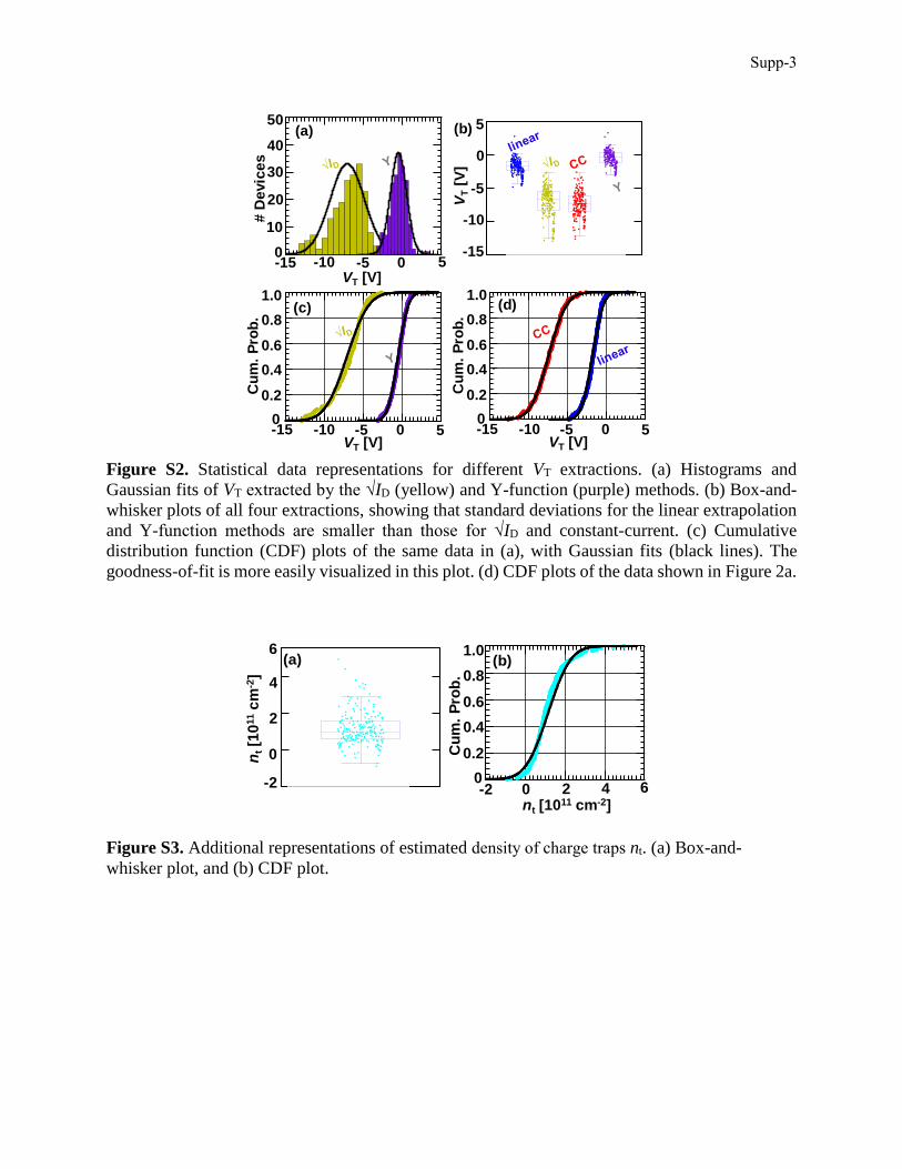
Figure S2. Statistical data representations for different VT extractions. (a) Histograms and
Gaussian fits of VT extracted by the √ID (yellow) and Y-function (purple) methods. (b) Box-and-
whisker plots of all four extractions, showing that standard deviations for the linear extrapolation
and Y-function methods are smaller than those for √ID and constant-current. (c) Cumulative
distribution function (CDF) plots of the same data in (a), with Gaussian fits (black lines). The
goodness-of-fit is more easily visualized in this plot. (d) CDF plots of the data shown in Figure 2a.
Figure S3. Additional representations of estimated density of charge traps nt. (a) Box-and-
whisker plot, and (b) CDF plot.
1 2 3 4
VT
[V]
-10
-15
-5
0
5
VT [V]50-5-10-15
# D
evic
es
50
40
30
20
10
0
VT [V]50-5-10-15
Cu
m.
Pro
b.
1.0
0.8
0.6
0.4
0.2
0
VT [V]50-5-10-15
Cu
m.
Pro
b.
1.0
0.8
0.6
0.4
0.2
0
(a) (b)
(c) (d)
1
nt[1
011
cm
-2]
2
0
-2
6
4
6nt [1011 cm-2]
20-2 4
1.0
0.8
0.6
0.4
0.2
0
Cu
m.
Pro
b.
(b)(a)

Supp-4
Figure S4. Additional representations of hysteresis extractions. (a) A mock-ID-VGS sweep with
over-exaggerated hysteresis, showing how we extract ΔVT and H. (b) ΔVT as measured by linear
extrapolation between the forward and backward ID-VGS sweep. These data correspond directly to
Figure 2b of the main text by nt = ΔVTCox/q. (c) Box-and-whisker plots of ΔVT and the maximum
measured hysteresis as taken between all points in the linear region of the forward and backward
ID-VGS sweeps. Given the definitions in (a), it is unsurprising that typical values for H would be
less than that for ΔVT. (d) CDF plots of the same data in (c) along with Gaussian and lognormal
fits (lines) for ΔVT and H, respectively.
It should be pointed out that, despite all values for H being positive as expected, 5% of the
extractions for ΔVT are negative. This is an artifact of the extraction methodology combined with
the fact that the hysteresis in our devices is indeed quite small. For any particular extraction of the
forward and backward values for VT, the 95% confidence intervals in the extraction (with the
coefficient of determination r2 ≥ 0.99999) overlap by 95%. Loosely put, there is a 95% chance that
the two values are the same, to 95% certainty in our measurement. This results in the error bars on
either side of any one ΔVT data point in Figures S4b-d being 20–25% greater than the mean value,
which would ideally be zero. This highlights the importance of taking measurements on large
numbers of data and running statistics. A more strict interpretation of the statistics will only lead
to the conclusion that, in addition to ΔVT being very small, we can only be 95% certain that the
population mean μΔVT is indeed positive. Compare to Figure S11e, where all extractions for ΔVT
and nt are positive.
1 2
Hys
tere
sis
[V
]
1.0
0.5
0
-0.5
ΔVT [V]1.00.50-0.5
# D
evic
es
50
40
30
20
10
0
Hysteresis [V]1.00.50-0.5
1.0
0.8
0.6
0.4
0.2
0
Cu
m.
Pro
b.
(b)
(c) (d)
1 2
VGS [V]-20 -10 0 10 20 30
I D[a
.u.]
ΔVT
H
(a)
Supp-5
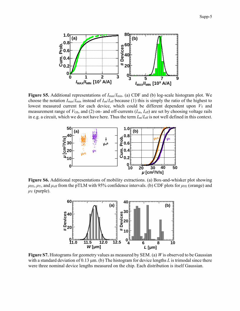
Figure S5. Additional representations of Imax/Imin. (a) CDF and (b) log-scale histogram plot. We
choose the notation Imax/Imin instead of Ion/Ioff because (1) this is simply the ratio of the highest to
lowest measured current for each device, which could be different dependent upon VT and
measurement range of VGS, and (2) on- and off-currents (Ion, Ioff) are set by choosing voltage rails
in e.g. a circuit, which we do not have here. Thus the term Ion/Ioff is not well defined in this context.
Figure S6. Additional representations of mobility extractions. (a) Box-and-whisker plot showing
μFE, μY, and μeff from the pTLM with 95% confidence intervals. (b) CDF plots for μFE (orange) and
μY (purple).
Figure S7. Histograms for geometry values as measured by SEM. (a) W is observed to be Gaussian
with a standard deviation of 0.13 μm. (b) The histogram for device lengths L is trimodal since there
were three nominal device lengths measured on the chip. Each distribution is itself Gaussian.
1.0
0.8
0.6
0.4
0.2
0
Cu
m.
Pro
b.
3IMAX/IMIN [107 A/A]
210
80
60
40
20
09
IMAX/IMIN [10X A/A]753
# D
evic
es
(b)(a)
1 2
μ[c
m2/V
/s]
20
10
0
50
30
40
1.0
0.8
0.6
0.4
0.2
0
Cu
m.
Pro
b.
50μ [cm2/V/s]
40302010
(a) (b)
40
30
20
10
010
L [μm]864
# D
evic
es
(b)
# D
evic
es
60
40
20
012.5
W [μm]12.011.511.0
(a)

Supp-6
Figure S8. Extractions for μFE assuming that L and W are their mean values for each device. (a)
While the mean is exactly the same, the variance of the histogram for μFE can be seen to increase
slightly with this assumption. The coefficient of variation (CV) only increases slightly due to L
and W having such small variances. (b) CDF plot of the data in (a), which may be contrasted to
the orange data in Figure S6b.
Figure S9. The histogram for RCY shows a mean near 3.0 kΩ·μm.
Figure S10. (a) pTLM analysis for VDS = 1.0 V. (b) RC = 2.1 ± 2.7 kΩ·μm at n = 1.6×1013 cm-2.
Inset: μeff = 34.7 ± 2.8 cm2/V/s. Colors represent increasing carrier density.
1.0
0.8
0.6
0.4
0.2
0
Cu
m.
Pro
b.
50μFE [cm2/V/s]
40302010
# D
evic
es
50
40
30
20
10
050
μFE [cm2/V/s]40302010
(a) (b)
80
60
40
20
06
RCY·W [kΩ·μm]420
# D
evic
es
8
n [1012 cm-2]15
0
20
40
µe
ff[c
m2/V
/s]
5 100
n [1012 cm-2]0 5 201510
RC
[kΩ
·μm
]
0
20
40
10
30
50
(b)
0 2 64 8 10L [μm]
RT
OT
[kΩ
·μm
]
0
200
400
100
300
(a)
20
60
Supp-7
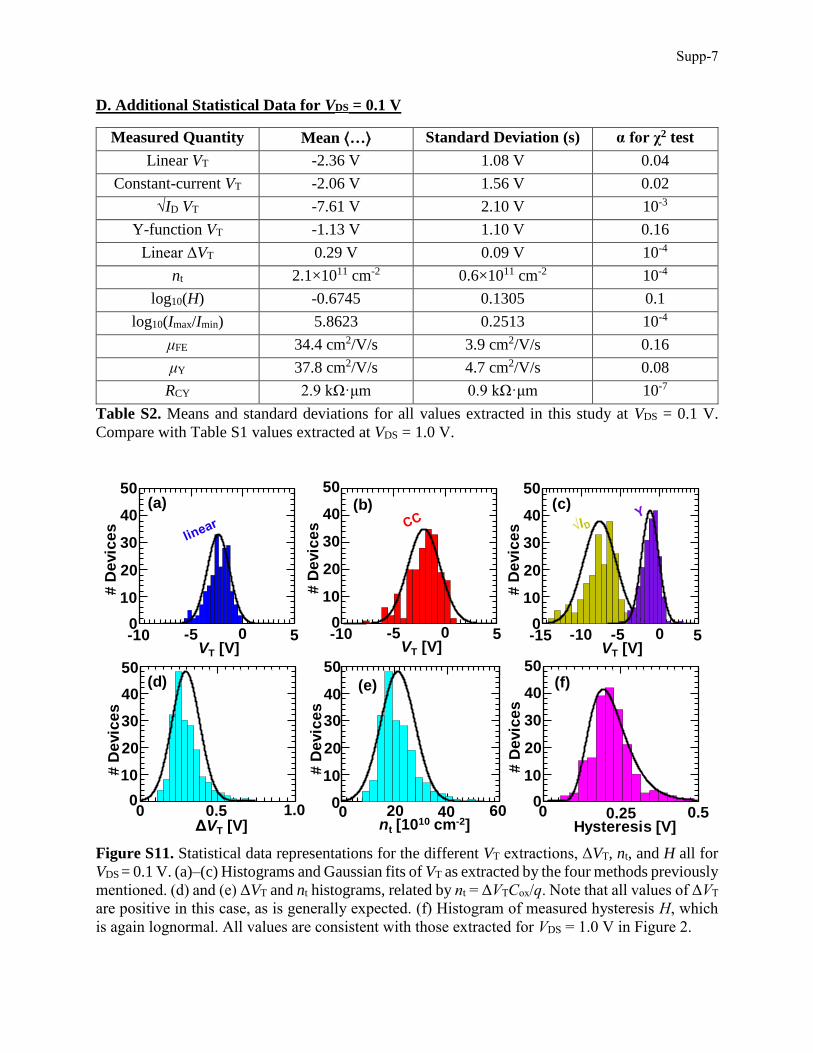
D. Additional Statistical Data for VDS = 0.1 V
Measured Quantity Mean ⟨…⟩ Standard Deviation (s) α for χ2 test
Linear VT -2.36 V 1.08 V 0.04
Constant-current VT -2.06 V 1.56 V 0.02
√ID VT -7.61 V 2.10 V 10-3
Y-function VT -1.13 V 1.10 V 0.16
Linear ΔVT 0.29 V 0.09 V 10-4
nt 2.1×1011 cm-2 0.6×1011 cm-2 10-4
log10(H) -0.6745 0.1305 0.1
log10(Imax/Imin) 5.8623 0.2513 10-4
μFE 34.4 cm2/V/s 3.9 cm2/V/s 0.16
μY 37.8 cm2/V/s 4.7 cm2/V/s 0.08
RCY 2.9 kΩ·μm 0.9 kΩ·μm 10-7
Table S2. Means and standard deviations for all values extracted in this study at VDS = 0.1 V.
Compare with Table S1 values extracted at VDS = 1.0 V.
Figure S11. Statistical data representations for the different VT extractions, ΔVT, nt, and H all for
VDS = 0.1 V. (a)–(c) Histograms and Gaussian fits of VT as extracted by the four methods previously
mentioned. (d) and (e) ΔVT and nt histograms, related by nt = ΔVTCox/q. Note that all values of ΔVT
are positive in this case, as is generally expected. (f) Histogram of measured hysteresis H, which
is again lognormal. All values are consistent with those extracted for VDS = 1.0 V in Figure 2.
VT [V]50-5-10
# D
evic
es
50
40
30
20
10
0
VT [V]50-5-10
# D
evic
es
50
40
30
20
10
0
VT [V]50-5-15
# D
evic
es
50
40
30
20
10
0-10
0.50.250
# D
evic
es
50
40
30
20
10
0
Hysteresis [V]ΔVT [V]1.00.50
# D
evic
es
50
40
30
20
10
0
# D
evic
es
50
40
30
20
10
0
nt [1010 cm-2]40200 60
(a) (b)
(d) (e)
(c)
(f)

Supp-8
Figure S12. Histograms for VDS = 0.1 V. (a) Histograms and lognormal fit of Imax/Imin. Note that
these values have fallen by approximately one order of magnitude compared to VDS = 1.0 V (see
Figure 2d in main text), since these devices are operating in triode and contact resistance is
relatively small. (b) μFE values are again the same as for VDS = 1.0 V (Figure 2e). (c) and (d),
mobility and contact resistance as extracted from the Y-function method (compare to Figure 2f at
VDS = 1.0 V).
E. Extractions Using the Y-Function Method
As expounded in Ref. S3, mobility can be estimated from the Y-function, mD / gIY , by the
expression
DSox
2
TGS
YVWC
L
VV
Y , where VT is estimated by linear extrapolation from a
plot of Y vs. VGS rather than ID vs. VGS. Further, an upper bound on the minimum single-contact
resistance in the strong inversion regime can be estimated by Yox
CY2
C
LWR , where θ is a VGS-
dependent attenuation factor with units of V-1 in the expression
DSTGSox
TGS
YD
1VVV
L
WC
VVI
. From these equations, we calculate μY = 38.2 ± 8.8
cm2/V/s and RCYW = 3.0 ± 1.4 kΩ·μm for VDS = 1.0 V.
60
40
20
0#
De
vic
es
3IMAX/IMIN [106 A/A]
210
# D
evic
es
50
40
30
20
10
050
μFE [cm2/V/s]40302010
# D
evic
es
50μY [cm2/V/s]
40302010
60
40
20
0
80
60
40
20
010
RCY·W [kΩ·μm]50
# D
evic
es
100
(a) (b)
(c) (d)

Supp-9
F. International Technology Roadmap (ITRS) specifications
In simulations, we optimize the flat band voltage of the top gate (VFB) for each channel length such
that the Ioff (at VGS = 0, VDS = VDD) = 100 nA/μm. Other device parameters used are as per ITRSS4
specifications as shown in the table below.
L (nm) tox (nm) VDD (V) RC (Ω·μm)
16 0.8 0.86 188
32 1.1 1.1 180
65 1.3 1.2 190
500 5.0 3.3 200
Table S3. The device parameters used to simulate MoS2 transistors with ITRS specifications.S4
G. Monte Carlo simulations of standard cells
Figure S13. Schematic for 2-input NAND and NOR gate
VDD
A B
A
B
VDD
2-input NAND gate 2-input NOR gate
A
B
A B

Supp-10
Figure S14. (a) to (f) show Monte Carlo simulations of fall time (𝜏Fall) and rise time (𝜏Rise) of
NOR2 for 16 nm and 65 nm technology nodes respectively. We have normalized the rise time and
fall time for each channel length with respective mean values. The performance corners [NFET-
PFET: Fast-Fast (FF), Slow-Slow (SS), Fast-Slow (FS) and Slow-Fast (SF)] are calculated for
⟨μFE⟩ ± 2sμFE. The simulated values for the performance corners are shown in red diamonds.
0.7 0.85 1 1.15 1.30.7
0.85
1
1.15
1.3
0.7 0.85 1 1.15 1.30.7
0.85
1
1.15
1.3
0.7 0.85 1 1.15 1.30.7
0.85
1
1.15
1.3
0.7 0.85 1 1.15 1.30.7
0.85
1
1.15
1.3
NAND
0.7 0.85 1 1.15 1.30.7
0.85
1
1.15
1.3
0.7 0.85 1 1.15 1.30.7
0.85
1
1.15
1.3
0.7 0.85 1 1.15 1.30.7
0.85
1
1.15
1.3
0.7 0.85 1 1.15 1.30.7
0.85
1
1.15
1.3
NOR
Norm. rise time
No
rm. fa
ll tim
e
Norm. rise time
No
rm. fa
ll tim
e
Norm. rise time
No
rm. fa
ll tim
e
Norm. rise time
No
rm. fa
ll tim
e
Norm. rise time
No
rm. fa
ll tim
e
Norm. rise time
No
rm. fa
ll tim
e
Norm. rise time
No
rm. fa
ll tim
e
Norm. rise time
No
rm. fa
ll tim
e
(a)
(b)
(c)
(d)
(f)
(g)
(h)
(i)
L = 16 nm
L = 32 nm
L = 65 nm
L = 500 nm
Supp-11
Supplementary References (S1) English, C. D.; Shine, G.; Dorgan, V. E.; Saraswat, K. C.; Pop, E. Improved Contacts to
MoS2 Field-Effect Transistors by Ultra-High Vacuum Metal Deposition. Nano Lett. 2016,
16, 3824–3830.
(S2) Smithe, K. K. H.; English, C. D.; Suryavanshi, S. V; Pop, E. Intrinsic Electrical Transport
and Performance Projections of Synthetic Monolayer MoS2 Devices. 2D Mater. 2017, 4,
011009.
(S3) Chang, H.-Y.; Zhu, W.; Akinwande, D. On the Mobility and Contact Resistance Evaluation
for Transistors Based on MoS2 or Two-Dimensional Semiconducting Atomic Crystals.
Appl. Phys. Lett. 2014, 104, 113504.
(S4) International Technology Roadmap for Semiconductors (ITRS). High Performance (HP)
and Low Power (LP) PIDS Tables. URL: <http://www.itrs2.net/itrs-reports.html>.