Embed Size (px)
Citation preview
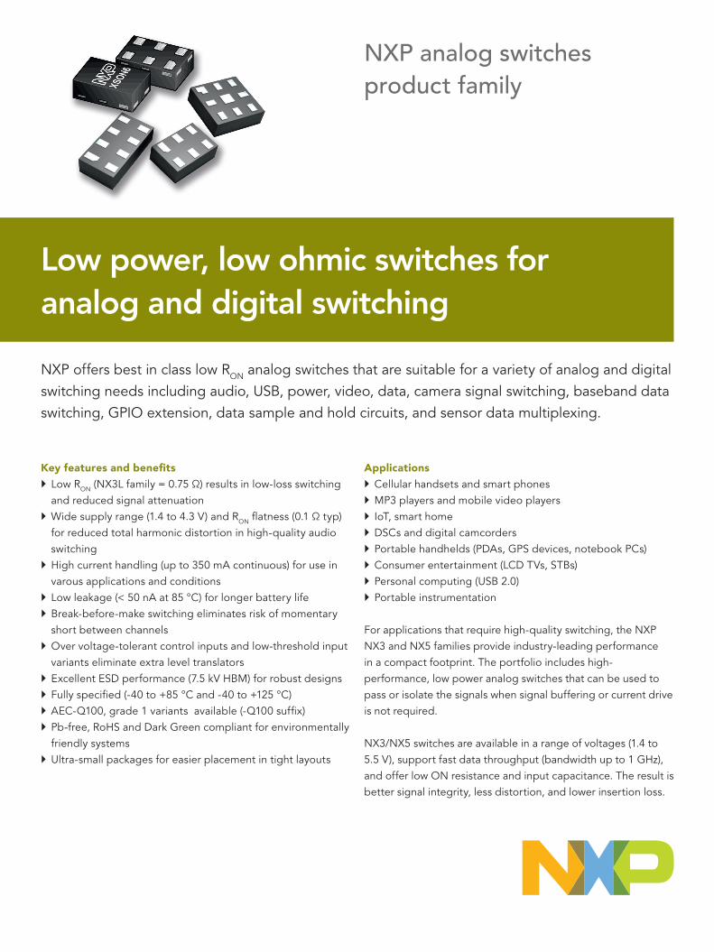
Low power, low ohmic switches for analog and digital switching
Key features and benefits ` Low RON (NX3L family = 0.75 Ω) results in low-loss switching and reduced signal attenuation
` Wide supply range (1.4 to 4.3 V) and RON flatness (0.1 Ω typ) for reduced total harmonic distortion in high-quality audio switching
` High current handling (up to 350 mA continuous) for use in varous applications and conditions
` Low leakage (< 50 nA at 85 °C) for longer battery life ` Break-before-make switching eliminates risk of momentary short between channels
` Over voltage-tolerant control inputs and low-threshold input variants eliminate extra level translators
` Excellent ESD performance (7.5 kV HBM) for robust designs ` Fully specified (-40 to +85 °C and -40 to +125 °C) ` AEC-Q100, grade 1 variants available (-Q100 suffix) ` Pb-free, RoHS and Dark Green compliant for environmentally friendly systems
` Ultra-small packages for easier placement in tight layouts
NXP offers best in class low RON analog switches that are suitable for a variety of analog and digital switching needs including audio, USB, power, video, data, camera signal switching, baseband data switching, GPIO extension, data sample and hold circuits, and sensor data multiplexing.
Applications ` Cellular handsets and smart phones ` MP3 players and mobile video players ` IoT, smart home ` DSCs and digital camcorders ` Portable handhelds (PDAs, GPS devices, notebook PCs) ` Consumer entertainment (LCD TVs, STBs) ` Personal computing (USB 2.0) ` Portable instrumentation
For applications that require high-quality switching, the NXP NX3 and NX5 families provide industry-leading performance in a compact footprint. The portfolio includes high-performance, low power analog switches that can be used to pass or isolate the signals when signal buffering or current drive is not required.
NX3/NX5 switches are available in a range of voltages (1.4 to 5.5 V), support fast data throughput (bandwidth up to 1 GHz), and offer low ON resistance and input capacitance. The result is better signal integrity, less distortion, and lower insertion loss.
NXP analog switches product family

NX3L and NX5L low ohmic switchesThe combination of low ON resistance and low RON flatnessof the NX3L devices greatly reduces switched signal attenuation and distortion, thus eliminating the need for buffer amplifiers in many applications.
0
0.4
0
0.8
1.2NX3L series
RON(Ω)
1 2 3 4 5VI (V)
0
0.2
2
3
4
5
6
7
8
10 1 2 3 4 5
0
0.4
0.6NX3V series
NX3DV series
RON(Ω)
RON(Ω)
1 2 3 4 5VI (V)
VI (V)
Measured at Tamp = 25°C
3.3 V 4.3 V
Vcc = 1.5 V
1.8 V
2.5 V 2.7 V
3.3 V
3.6 V
4.3 V
4.3 V
Vcc = 1.5 V
Vcc = 1.4 V
1.8 V
1.65 V
2.5 V
2.5 V
2.7 V
3.0 V
NX3L typical ON resistance v switch input voltage
When switching 2 V audio signals to a 32 Ω speaker at a supply voltage of 2.7 V, the NX3L series has a typical attenuation of 0.13 dB and a typical distortion of 0.024%.
NX3L switches are fabricated in a 0.35 μm CMOS technology that delivers a wide supply range (1.4 to 4.3 V), low leakage and very low static and dynamic power dissipation. This makes the NX3L devices especially well suited for portable applications. Very low switch leakage (< 50 nA) also makes them an excellent choice for data monitoring and analog sensing applications.
NX3DV & NX5DV data/video switchesNX3DV and NX5DV are higher bandwidth data video switches. They are well suited for applications that switch analog VGA signals between a graphics controller and multiple displays or that multiplex audio, USB, and UART signals via a single connector.
The NX5DV715 is a dual supply 1-of-2 VGA switch which integrates high-bandwidth SPDT switches with level-translating buffers and level translating switches to provide switching of input RGB, H-Sync, V-Sync and DDC signals to either of two output channels.
The NX3DV221 (see eye diagram below) and NX3DV42 are designed for the switching of USB 2.0 signals in handset and consumer applications.
NX3DV221 USB2.0 eye diagram
All NX3 and NX5 products have control inputs with Schmitt-trigger action making them tolerant to slower input rise and fall times (up to 200 ns/V). To support mixed-voltage applications, the NX3LnT and NX3DV products have low threshold control inputs. This allows a 1.8 V controller to drive a 3.3 V switch without any external translator devices.
To improve placement and routing these switches are offered in small footprint PicoGate, MicroPak and leadless QFN packages, making them a solution for applications where board space and headroom are at a premium.
The NX3 and NX5 range also includes devices that are automotive qualified per AEC-Q100 grade 1.
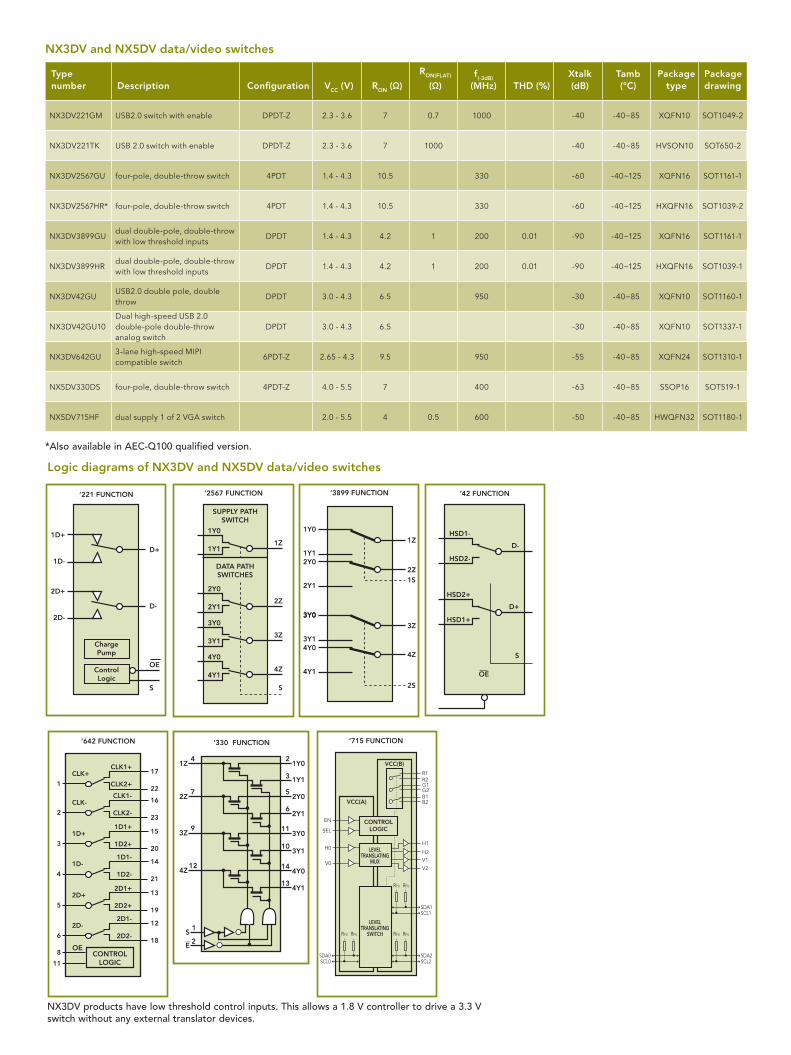
Type number Description Configuration VCC (V) RON (Ω)
RON(FLAT)
(Ω)f(-3dB)
(MHz) THD (%)Xtalk (dB)
Tamb (°C)
Package type
Package drawing
NX3DV221GM USB2.0 switch with enable DPDT-Z 2.3 - 3.6 7 0.7 1000 -40 -40~85 XQFN10 SOT1049-2
NX3DV221TK USB 2.0 switch with enable DPDT-Z 2.3 - 3.6 7 1000 -40 -40~85 HVSON10 SOT650-2
NX3DV2567GU four-pole, double-throw switch 4PDT 1.4 - 4.3 10.5 330 -60 -40~125 XQFN16 SOT1161-1
NX3DV2567HR* four-pole, double-throw switch 4PDT 1.4 - 4.3 10.5 330 -60 -40~125 HXQFN16 SOT1039-2
NX3DV3899GUdual double-pole, double-throw with low threshold inputs
DPDT 1.4 - 4.3 4.2 1 200 0.01 -90 -40~125 XQFN16 SOT1161-1
NX3DV3899HRdual double-pole, double-throw with low threshold inputs
DPDT 1.4 - 4.3 4.2 1 200 0.01 -90 -40~125 HXQFN16 SOT1039-1
NX3DV42GUUSB2.0 double pole, double throw
DPDT 3.0 - 4.3 6.5 950 -30 -40~85 XQFN10 SOT1160-1
NX3DV42GU10Dual high-speed USB 2.0 double-pole double-throw analog switch
DPDT 3.0 - 4.3 6.5 -30 -40~85 XQFN10 SOT1337-1
NX3DV642GU3-lane high-speed MIPI compatible switch
6PDT-Z 2.65 - 4.3 9.5 950 -55 -40~85 XQFN24 SOT1310-1
NX5DV330DS four-pole, double-throw switch 4PDT-Z 4.0 - 5.5 7 400 -63 -40~85 SSOP16 SOT519-1
NX5DV715HF dual supply 1 of 2 VGA switch 2.0 - 5.5 4 0.5 600 -50 -40~85 HWQFN32 SOT1180-1
NX3DV and NX5DV data/video switches
Logic diagrams of NX3DV and NX5DV data/video switches
‘1G3157 FUNCTION'1T3157 FUNCTION'1T5157 FUNCTION
‘1G384 FUNCTION'1T384 FUNCTION
‘4357 FUNCTION ‘4684 FUNCTION‘2267 ’2750
‘2G384 FUNCTION
‘1G53 FUNCTION'1T53 FUNCTION
‘1G66 FUNCTION ‘2G66 FUNCTION’2T66 FUNCTION
Y1
Y0
S
Y0
Y1
Y22Y1
2Y0
Z
Z
Y1
Y0
S E
E2S
E
YY1
Y0
Z
E
EE0
E1
Z
Z
Z1
2Z
E0
Z0
Y1
Y0
Z1
Z01Y1
1Y0
1S
1Z
‘2467 FUNCTION
1Y0
1Y12Y0
3Y0
2Y1
1Z
2Z1S
3Y0
3Y14Y0
4Y1
3Z
4Z2S
‘3899 FUNCTION
1Y0
1Y12Y0
3Y0
2Y1
1Z
2Z1S
3Y0
3Y14Y0
4Y1
3Z
4Z
2S
‘2567 FUNCTION
1Y0
1Y11Z
2Y0
2Y12Z
3Y0
3Y13Z
4Y0
4Y14Z
S
SUPPLY PATHSWITCH
DATA PATHSWITCHES
‘4053 FUNCTION/E
1Y0
1Y11Z
S1
2Y0
2Y12Z
S2
3Y0
3Y13Z
S3
‘42 FUNCTION
HSD1-
HSD2-
D-
S
HSD2+
HSD1+
D+
OE
‘642 FUNCTION
CLK1+CLK+ 17
CLK2+22
1
CLK1-CLK- 16
CLK2-23
2
1D1+1D+ 15
1D2+20
3
1D1-1D- 14
1D2-21
4
2D1+2D+ 13
2D2+19
5
2D1-2D- 12
2D2-18
6
8
11
OECONTROL
LOGIC
‘221 FUNCTION
ChargePump
1D+
1D-
D+
2D+
2D-
D-
S
OEControlLogic
‘715 FUNCTION
EN
VCC(B)
VCC(A)
H1
R1R2G1G2B1B2
H2V1
V2
SEL
LEVELTRANSLATING
MUX
LEVELTRANSLATING
SWITCH
H0
V0
SDA0
RPU
SCL0SDA2SCL2
SDA1SCL1
RPU RPU RPU
RPU RPU
CONTROL LOGIC
‘4051 FUNCTION
Y0
Y1
Y2
Y3
Y4
Y5
Y6
Y7
Z
/E
S1S2S3
‘330 FUNCTION
1Z 1Y04 2
2Z 2Y0
1Y1
7
3Z9
4Z12
S1
E 2
5
3
2Y16
3Y011
3Y110
4Y014
4Y113
*Also available in AEC-Q100 qualified version.
NX3DV products have low threshold control inputs. This allows a 1.8 V controller to drive a 3.3 V switch without any external translator devices.

Type number Description Configuration VCC (V) RON (Ω)
RON(FLAT)
(Ω)f(-3dB)
(MHz) THD (%)Xtalk (dB)
Tamb (°C)
Package type
Package drawing
NX3L1G3157GM single-pole, double-throw SPDT-Z 1.4 - 4.3 0.75 0.3 60 0.0024 -90 -40~125 XSON6 SOT886
NX3L1G384GM single-pole, single-throw SPST-NC 1.4 - 4.3 0.75 0.3 60 0.0024 -90 -40~125 XSON6 SOT886
NX3L1G53GM single-pole, double-throw SPDT-Z 1.4 - 4.3 0.75 0.3 60 0.0024 -90 -40~125 XQFN8 SOT902-1
NX3L1G53GT single-pole, double-throw SPDT-Z 1.4 - 4.3 0.75 0.3 60 0.0024 -90 -40~125 XSON8 SOT833-1
NX3L1G66GM single-pole, single-throw SPST-NO 1.4 - 4.3 0.75 0.3 60 0.0024 -90 -40~125 XSON6 SOT886
NX3L1T3157GM single-pole, double-throw with low threshold inputs SPDT 1.4 - 4.3 0.75 0.3 60 0.0024 -90 -40~125 XSON6 SOT886
NX3L1T384GM single-pole, single-throw with low threshold inputs SPST-NC 1.4 - 4.3 0.75 0.3 60 0.0024 -90 -40~125 XSON6 SOT886
NX3L1T5157GM single-pole, double-throw with low threshold inputs SPDT 1.4 - 4.3 0.75 0.3 60 0.0024 -90 -40~125 XSON6 SOT886
NX3L1T53GM single-pole, double-throw with low threshold inputs SPDT-Z 1.4 - 4.3 0.75 0.3 60 0.0024 -90 -40~125 XQFN8 SOT902-1
NX3L1T53GT single-pole, double-throw with low threshold inputs SPDT-Z 1.4 - 4.3 0.75 0.3 60 0.0024 -90 -40~125 XSON8 SOT833-1
NX3L2267GM dual single-pole double-throw with low threshold inputs SPDT 1.4 - 4.3 0.75 0.3 60 0.02 -90 -40~125 XQFN10 SOT1049-3
NX3L2267GU dual single-pole double-throw with low threshold inputs SPDT 1.4 - 4.3 0.75 0.3 60 0.02 -90 -40~125 XQFN10 SOT1160-1
NX3L2267SGU dual single-pole double-throw with low threshold inputs SPDT 1.4 - 4.3 0.75 0.3 60 0.02 -90 -40~125 XQFN10 SOT1160-1
NX3L2467GU dual double-pole, double-throw with low threshold inputs DPDT 1.4 - 4.3 0.75 0.3 60 0.01 -90 -40~125 XQFN16 SOT1161-1
NX3L2467HR dual double-pole, double-throw with low threshold inputs DPDT 1.4 - 4.3 0.75 0.3 60 0.01 -90 -40~125 HXQFN16 SOT1039-1
NX3L2467PW dual double-pole, double-throw with low threshold inputs DPDT 1.4 - 4.3 0.75 0.3 60 0.01 -90 -40~125 TSSOP16 SOT403-1
NX3L2G384GM dual single-pole, single-throw SPST-NC 1.4 - 4.3 0.75 0.3 60 0.0024 -90 -40~125 XQFN8 SOT902-1
NX3L2G384GT dual single-pole, single-throw SPST-NC 1.4 - 4.3 0.75 0.3 60 0.0024 -90 -40~125 XSON8 SOT833-1
NX3L2G66GT dual single-pole, single-throw SPST-NO 1.4 - 4.3 0.75 0.3 60 0.0024 -90 -40~125 XSON8 SOT833-1
NX3L2T66GM dual single-pole, single-throw with low threshold inputs SPST-NO 1.4 - 4.3 0.75 0.3 60 0.0024 -90 -40~125 XQFN8 SOT902-1
NX3L2T66GT dual single-pole, single-throw with low threshold inputs SPST-NO 1.4 - 4.3 0.75 0.3 60 0.0024 -90 -40~125 XSON8 SOT833-1
NX3L4051HR* single-pole, octal-throw SP8T-Z 1.4 - 4.3 0.75 0.3 15 0.02 -90 -40~125 HXQFN16 SOT1039-1
NX3L4051PW* single-pole, octal-throw SP8T-Z 1.4 - 4.3 0.75 0.3 15 0.02 -90 -40~125 TSSOP16 SOT403-1
NX3L4053HR* triple single-pole, double-throw SPDT-Z 1.4 - 4.3 0.8 0.3 60 0.02 -90 -40~125 HXQFN16 SOT1039-1
NX3L4053PW* triple single-pole, double-throw SPDT-Z 1.4 - 4.3 0.8 0.3 60 0.02 -90 -40~125 TSSOP16 SOT403-1
NX3L4357GM single-pole, triple-throw with low threshold inputs SP3T-Z 1.4 - 4.3 0.75 0.35 30 0.02 -90 -40~125 XQFN10 SOT1049-2
NX3L4684GM dual single-pole double-throw with low threshold inputs SPDT 1.4 - 4.3 0.8 0.3 25 0.01 -90 -40~125 XQFN10 SOT1049-3
NX3L4684TK dual single-pole double-throw with low threshold inputs SPDT 1.4 - 4.3 0.8 0.3 25 0.01 -90 -40~125 HVSON10 SOT650-2
NX5L2750CGU single-pole double-throw audio, negative swing SPDT 1.8 - 5.0 0.8 0.3 100 0.03 -60 -40~85 XQFN10 SOT1160-1
NX3L and NX5L low-ohmic analog switches
*Also available in AEC-Q100 qualified version.
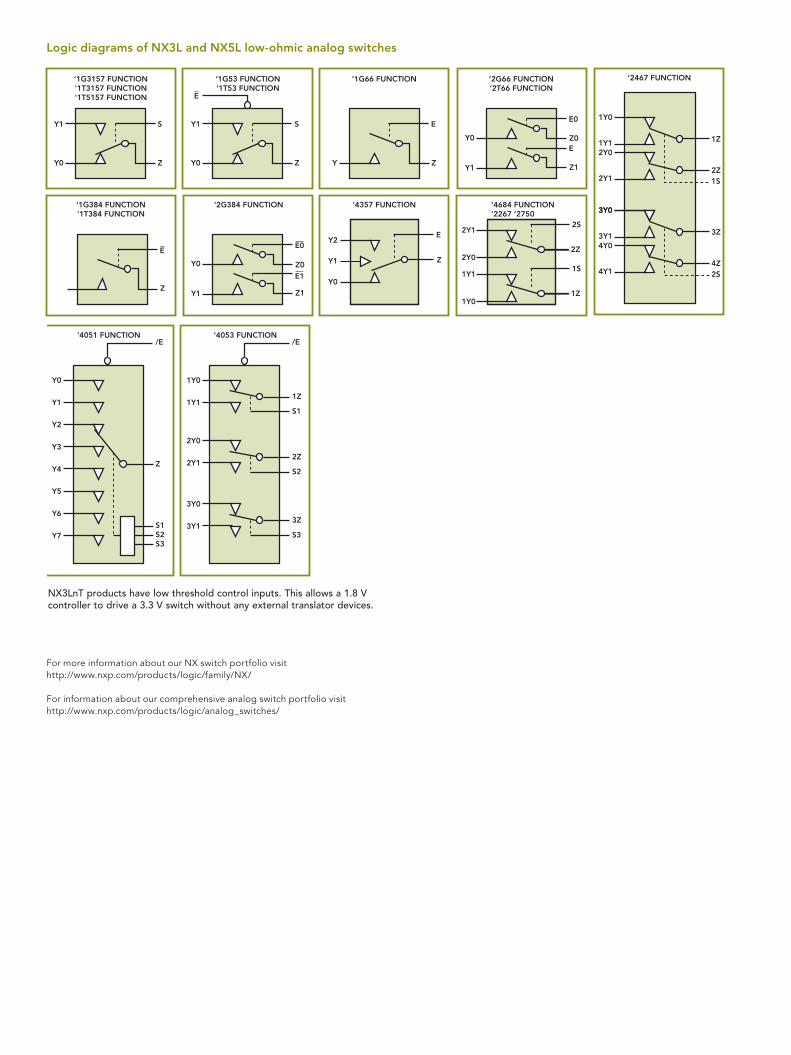
Logic diagrams of NX3L and NX5L low-ohmic analog switches
‘1G3157 FUNCTION'1T3157 FUNCTION'1T5157 FUNCTION
‘1G384 FUNCTION'1T384 FUNCTION
‘4357 FUNCTION ‘4684 FUNCTION‘2267 ’2750
‘2G384 FUNCTION
‘1G53 FUNCTION'1T53 FUNCTION
‘1G66 FUNCTION ‘2G66 FUNCTION’2T66 FUNCTION
Y1
Y0
S
Y0
Y1
Y22Y1
2Y0
Z
Z
Y1
Y0
S E
E2S
E
YY1
Y0
Z
E
EE0
E1
Z
Z
Z1
2Z
E0
Z0
Y1
Y0
Z1
Z01Y1
1Y0
1S
1Z
‘2467 FUNCTION
1Y0
1Y12Y0
3Y0
2Y1
1Z
2Z1S
3Y0
3Y14Y0
4Y1
3Z
4Z2S
‘3899 FUNCTION
1Y0
1Y12Y0
3Y0
2Y1
1Z
2Z1S
3Y0
3Y14Y0
4Y1
3Z
4Z
2S
‘2567 FUNCTION
1Y0
1Y11Z
2Y0
2Y12Z
3Y0
3Y13Z
4Y0
4Y14Z
S
SUPPLY PATHSWITCH
DATA PATHSWITCHES
‘4053 FUNCTION/E
1Y0
1Y11Z
S1
2Y0
2Y12Z
S2
3Y0
3Y13Z
S3
‘42 FUNCTION
HSD1-
HSD2-
D-
S
HSD2+
HSD1+
D+
OE
‘642 FUNCTION
CLK1+CLK+ 17
CLK2+22
1
CLK1-CLK- 16
CLK2-23
2
1D1+1D+ 15
1D2+20
3
1D1-1D- 14
1D2-21
4
2D1+2D+ 13
2D2+19
5
2D1-2D- 12
2D2-18
6
8
11
OECONTROL
LOGIC
‘221 FUNCTION
ChargePump
1D+
1D-
D+
2D+
2D-
D-
S
OEControlLogic
‘715 FUNCTION
EN
VCC(B)
VCC(A)
H1
R1R2G1G2B1B2
H2V1
V2
SEL
LEVELTRANSLATING
MUX
LEVELTRANSLATING
SWITCH
H0
V0
SDA0
RPU
SCL0SDA2SCL2
SDA1SCL1
RPU RPU RPU
RPU RPU
CONTROL LOGIC
‘4051 FUNCTION
Y0
Y1
Y2
Y3
Y4
Y5
Y6
Y7
Z
/E
S1S2S3
‘330 FUNCTION
1Z 1Y04 2
2Z 2Y0
1Y1
7
3Z9
4Z12
S1
E 2
5
3
2Y16
3Y011
3Y110
4Y014
4Y113
For more information about our NX switch portfolio visithttp://www.nxp.com/products/logic/family/NX/
For information about our comprehensive analog switch portfolio visithttp://www.nxp.com/products/logic/analog_switches/
NX3LnT products have low threshold control inputs. This allows a 1.8 V controller to drive a 3.3 V switch without any external translator devices.
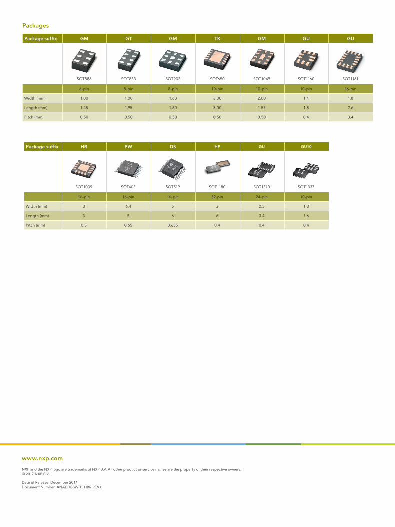
Package suffix GM GT GM TK GM GU GU
SOT886 SOT833 SOT902 SOT650 SOT1049 SOT1160 SOT1161
6-pin 8-pin 8-pin 10-pin 10-pin 10-pin 16-pin
Width (mm) 1.00 1.00 1.60 3.00 2.00 1.4 1.8
Length (mm) 1.45 1.95 1.60 3.00 1.55 1.8 2.6
Pitch (mm) 0.50 0.50 0.50 0.50 0.50 0.4 0.4
Package suffix HR PW DS HF GU GU10
SOT1039 SOT403 SOT519 SOT1180 SOT1310 SOT1337
16-pin 16-pin 16-pin 32-pin 24-pin 10-pin
Width (mm) 3 6.4 5 3 2.5 1.3
Length (mm) 3 5 6 6 3.4 1.6
Pitch (mm) 0.5 0.65 0.635 0.4 0.4 0.4
Packages
www.nxp.com
NXP and the NXP logo are trademarks of NXP B.V. All other product or service names are the property of their respective owners. © 2017 NXP B.V.
Date of Release: December 2017 Document Number: ANALOGSWITCHBR REV 0