Embed Size (px)
Citation preview
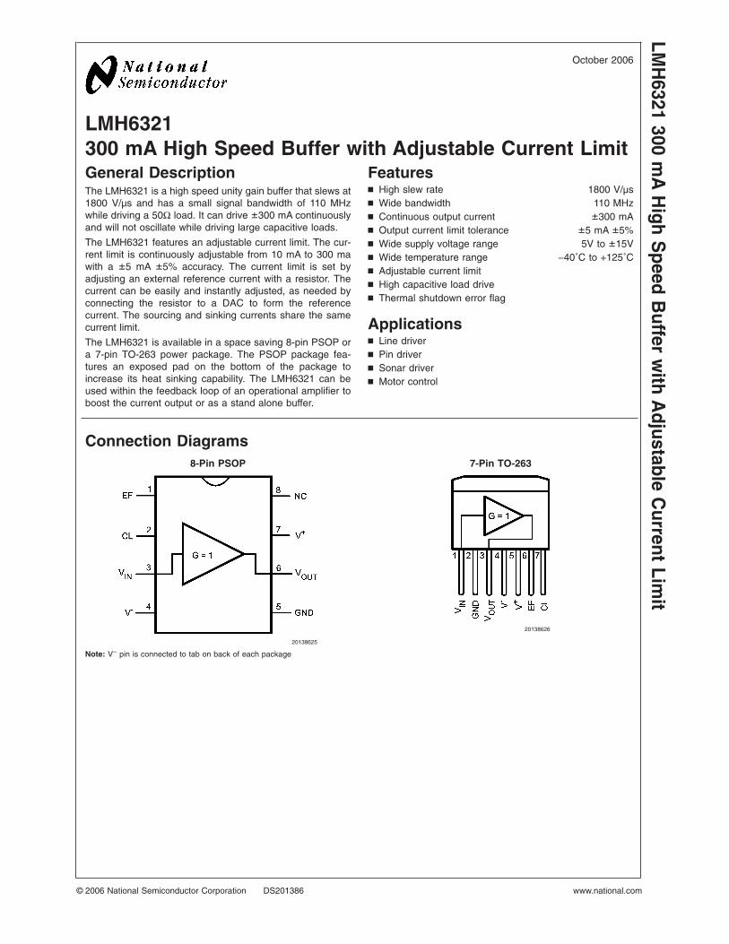
LMH6321300 mA High Speed Buffer with Adjustable Current LimitGeneral DescriptionThe LMH6321 is a high speed unity gain buffer that slews at1800 V/µs and has a small signal bandwidth of 110 MHzwhile driving a 50Ω load. It can drive ±300 mA continuouslyand will not oscillate while driving large capacitive loads.
The LMH6321 features an adjustable current limit. The cur-rent limit is continuously adjustable from 10 mA to 300 mawith a ±5 mA ±5% accuracy. The current limit is set byadjusting an external reference current with a resistor. Thecurrent can be easily and instantly adjusted, as needed byconnecting the resistor to a DAC to form the referencecurrent. The sourcing and sinking currents share the samecurrent limit.
The LMH6321 is available in a space saving 8-pin PSOP ora 7-pin TO-263 power package. The PSOP package fea-tures an exposed pad on the bottom of the package toincrease its heat sinking capability. The LMH6321 can beused within the feedback loop of an operational amplifier toboost the current output or as a stand alone buffer.
Featuresn High slew rate 1800 V/µsn Wide bandwidth 110 MHzn Continuous output current ±300 mAn Output current limit tolerance ±5 mA ±5%n Wide supply voltage range 5V to ±15Vn Wide temperature range −40˚C to +125˚Cn Adjustable current limitn High capacitive load driven Thermal shutdown error flag
Applicationsn Line drivern Pin drivern Sonar drivern Motor control
Connection Diagrams8-Pin PSOP 7-Pin TO-263
20138625
20138626
Note: V− pin is connected to tab on back of each package
October 2006LM
H6321
300m
AH
ighS
peedB
ufferw
ithA
djustableC
urrentLim
it
© 2006 National Semiconductor Corporation DS201386 www.national.com
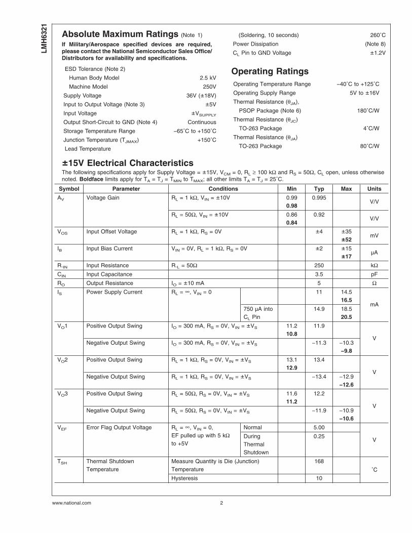
Absolute Maximum Ratings (Note 1)
If Military/Aerospace specified devices are required,please contact the National Semiconductor Sales Office/Distributors for availability and specifications.
ESD Tolerance (Note 2)
Human Body Model 2.5 kV
Machine Model 250V
Supply Voltage 36V (±18V)
Input to Output Voltage (Note 3) ±5V
Input Voltage ±VSUPPLY
Output Short-Circuit to GND (Note 4) Continuous
Storage Temperature Range −65˚C to +150˚C
Junction Temperature (TJMAX) +150˚C
Lead Temperature
(Soldering, 10 seconds) 260˚C
Power Dissipation (Note 8)
CL Pin to GND Voltage ±1.2V
Operating RatingsOperating Temperature Range −40˚C to +125˚C
Operating Supply Range 5V to ±16V
Thermal Resistance (θJA),
PSOP Package (Note 6) 180˚C/W
Thermal Resistance (θJC)
TO-263 Package 4˚C/W
Thermal Resistance (θJA)
TO-263 Package 80˚C/W
±15V Electrical CharacteristicsThe following specifications apply for Supply Voltage = ±15V, VCM = 0, RL ≥ 100 kΩ and RS = 50Ω, CL open, unless otherwisenoted. Boldface limits apply for TA = TJ = TMIN to TMAX; all other limits TA = TJ = 25˚C.
Symbol Parameter Conditions Min Typ Max Units
AV Voltage Gain RL = 1 kΩ, VIN = ±10V 0.990.98
0.995V/V
RL = 50Ω, VIN = ±10V 0.860.84
0.92V/V
VOS Input Offset Voltage RL = 1 kΩ, RS = 0V ±4 ±35±52
mV
IB Input Bias Current VIN = 0V, RL = 1 kΩ, RS = 0V ±2 ±15±17
µA
R.IN Input Resistance R.L = 50Ω 250 kΩCIN Input Capacitance 3.5 pF
RO Output Resistance IO = ±10 mA 5 ΩIS Power Supply Current RL = ∞, VIN = 0 11 14.5
16.5mA
750 µA intoCL Pin
14.9 18.520.5
VO1 Positive Output Swing IO = 300 mA, RS = 0V, VIN = ±VS 11.210.8
11.9
VNegative Output Swing IO = 300 mA, RS = 0V, VIN = ±VS −11.3 −10.3
−9.8
VO2 Positive Output Swing RL = 1 kΩ, RS = 0V, VIN = ±VS 13.112.9
13.4
VNegative Output Swing RL = 1 kΩ, RS = 0V, VIN = ±VS −13.4 −12.9
−12.6
VO3 Positive Output Swing RL = 50Ω, RS = 0V, VIN = ±VS 11.611.2
12.2
VNegative Output Swing RL = 50Ω, RS = 0V, VIN = ±VS −11.9 −10.9
−10.6
VEF Error Flag Output Voltage RL = ∞, VIN = 0,EF pulled up with 5 kΩto +5V
Normal 5.00
VDuringThermalShutdown
0.25
TSH Thermal ShutdownTemperature
Measure Quantity is Die (Junction)Temperature
168
˚C
Hysteresis 10
LMH
6321
www.national.com 2
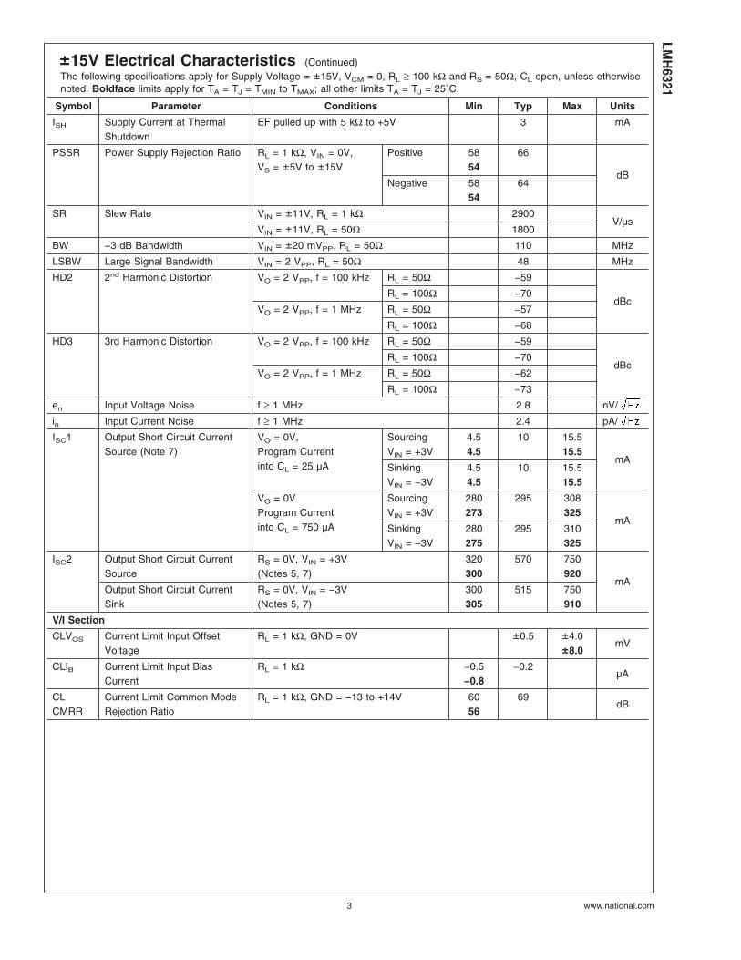
±15V Electrical Characteristics (Continued)The following specifications apply for Supply Voltage = ±15V, VCM = 0, RL ≥ 100 kΩ and RS = 50Ω, CL open, unless otherwisenoted. Boldface limits apply for TA = TJ = TMIN to TMAX; all other limits TA = TJ = 25˚C.
Symbol Parameter Conditions Min Typ Max Units
ISH Supply Current at ThermalShutdown
EF pulled up with 5 kΩ to +5V 3 mA
PSSR Power Supply Rejection Ratio RL = 1 kΩ, VIN = 0V,VS = ±5V to ±15V
Positive 5854
66
dBNegative 58
5464
SR Slew Rate VIN = ±11V, RL = 1 kΩ 2900V/µs
VIN = ±11V, RL = 50Ω 1800
BW −3 dB Bandwidth VIN = ±20 mVPP, RL = 50Ω 110 MHz
LSBW Large Signal Bandwidth VIN = 2 VPP, RL = 50Ω 48 MHz
HD2 2nd Harmonic Distortion VO = 2 VPP, f = 100 kHz RL = 50Ω −59
dBcRL = 100Ω −70
VO = 2 VPP, f = 1 MHz RL = 50Ω −57
RL = 100Ω −68
HD3 3rd Harmonic Distortion VO = 2 VPP, f = 100 kHz RL = 50Ω −59
dBcRL = 100Ω −70
VO = 2 VPP, f = 1 MHz RL = 50Ω −62
RL = 100Ω −73
en Input Voltage Noise f ≥ 1 MHz 2.8 nV/
in Input Current Noise f ≥ 1 MHz 2.4 pA/
ISC1 Output Short Circuit CurrentSource (Note 7)
VO = 0V,Program Currentinto CL = 25 µA
SourcingVIN = +3V
4.54.5
10 15.515.5
mASinkingVIN = −3V
4.54.5
10 15.515.5
VO = 0VProgram Currentinto CL = 750 µA
SourcingVIN = +3V
280273
295 308325
mASinkingVIN = −3V
280275
295 310325
ISC2 Output Short Circuit CurrentSource
RS = 0V, VIN = +3V(Notes 5, 7)
320300
570 750920
mAOutput Short Circuit CurrentSink
RS = 0V, VIN = −3V(Notes 5, 7)
300305
515 750910
V/I Section
CLVOS Current Limit Input OffsetVoltage
RL = 1 kΩ, GND = 0V ±0.5 ±4.0±8.0
mV
CLIB Current Limit Input BiasCurrent
RL = 1 kΩ −0.5−0.8
−0.2µA
CLCMRR
Current Limit Common ModeRejection Ratio
RL = 1 kΩ, GND = −13 to +14V 6056
69dB
LMH
6321
www.national.com3
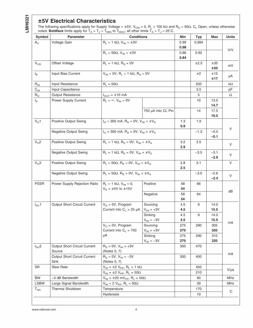
±5V Electrical CharacteristicsThe following specifications apply for Supply Voltage = ±5V, VCM = 0, RL ≥ 100 kΩ and RS = 50Ω, CL Open, unless otherwisenoted. Boldface limits apply for TA = TJ = TMIN to TMAX; all other limits TA = TJ = 25˚C.
Symbol Parameter Conditions Min Typ Max Units
AV Voltage Gain RL = 1 kΩ, VIN = ±3V 0.990.98
0.994
V/VRL = 50Ω, VIN = ±3V 0.86
0.840.92
VOS Offset Voltage RL = 1 kΩ, RS = 0V ±2.5 ±35±50
mV
IB Input Bias Current VIN = 0V, RL = 1 kΩ, RS = 0V ±2 ±15±17
µA
RIN Input Resistance RL = 50Ω 250 kΩCIN Input Capacitance 3.5 pF
RO Output Resistance IOUT = ±10 mA 5 ΩIS Power Supply Current RL = ∞, VIN = 0V 10 13.5
14.7
750 µA into CL Pin 14 17.519.5
VO1 Positive Output Swing IO = 300 mA, RS = 0V, VIN = ±VS 1.30.9
1.9
VNegative Output Swing IO = 300 mA, RS = 0V, VIN = ±VS −1.3 −0.5
−0.1
VO2 Positive Output Swing RL = 1 kΩ, RS = 0V, VIN = ±VS 3.22.9
3.5V
Negative Output Swing RL = 1 kΩ, RS = 0V, VIN = ±VS −3.5 −3.1−2.9
V
VO3 Positive Output Swing RL = 50Ω, RS = 0V, VIN = ±VS 2.82.5
3.1 V
Negative Output Swing RL = 50Ω, RS = 0V, VIN = ±VS −3.0 −2.6−2.4
V
PSSR Power Supply Rejection Ratio RL = 1 kΩ, VIN = 0,VS = ±5V to ±15V
Positive 5854
66
dBNegative 58
5464
ISC1 Output Short Circuit Current VO = 0V, ProgramCurrent into CL = 25 µA
SourcingVIN = +3V
4.54.5
9 14.015.5
mA
SinkingVIN = −3V
4.54.5
9 14.015.5
VO = 0V, ProgramCurrent into CL = 750µA
SourcingVIN = +3V
275270
290 305320
SinkingVIN = −3V
275270
290 310320
ISC2 Output Short Circuit CurrentSource
RS = 0V, VIN = +3V(Notes 5, 7)
300 470
mAOutput Short Circuit CurrentSink
RS = 0V, VIN = −3V(Notes 5, 7)
300 400
SR Slew Rate VIN = ±2 VPP, RL = 1 kΩ 450V/µs
VIN = ±2 VPP, RL = 50Ω 210
BW −3 dB Bandwidth VIN = ±20 mVPP, RL = 50Ω 90 MHz
LSBW Large Signal Bandwidth VIN = 2 VPP, RL = 50Ω 39 MHz
TSD Thermal Shutdown Temperature 170˚C
Hysteresis 10
LMH
6321
www.national.com 4
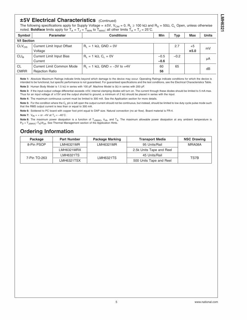
±5V Electrical Characteristics (Continued)The following specifications apply for Supply Voltage = ±5V, VCM = 0, RL ≥ 100 kΩ and RS = 50Ω, CL Open, unless otherwisenoted. Boldface limits apply for TA = TJ = TMIN to TMAX; all other limits TA = TJ = 25˚C.
Symbol Parameter Conditions Min Typ Max Units
V/I Section
CLVOS Current Limit Input OffsetVoltage
RL = 1 kΩ, GND = 0V 2.7 +5±5.0
mV
CLIB Current Limit Input BiasCurrent
RL = 1 kΩ, CL = 0V −0.5−0.6
−0.2µA
CLCMRR
Current Limit Common ModeRejection Ratio
RL = 1 kΩ, GND = −3V to +4V 6056
65dB
Note 1: Absolute Maximum Ratings indicate limits beyond which damage to the device may occur. Operating Ratings indicate conditions for which the device isintended to be functional, but specific performance is not guaranteed. For guaranteed specifications and the test conditions, see the Electrical Characteristics Table.
Note 2: Human Body Model is 1.5 kΩ in series with 100 pF. Machine Model is 0Ω in series with 200 pF.
Note 3: If the input-output voltage differential exceeds ±5V, internal clamping diodes will turn on. The current through these diodes should be limited to 5 mA max.Thus for an input voltage of ±15V and the output shorted to ground, a minimum of 2 kΩ should be placed in series with the input.
Note 4: The maximum continuous current must be limited to 300 mA. See the Application section for more details.
Note 5: For the condition where the CL pin is left open the output current should not be continuous, but instead, should be limited to low duty cycle pulse mode suchthat the RMS output current is less than or equal to 300 mA.
Note 6: Soldered to PC board with copper foot print equal to DAP size. Natural convection (no air flow). Board material is FR-4.
Note 7: VIN = + or −4V at TJ = −40˚C.
Note 8: The maximum power dissipation is a function of TJ(MAX), θJA, and TA. The maximum allowable power dissipation at any ambient temperature isPD = TJ(MAX)–TA)/θJA. See Thermal Management section of the Application Hints.
Ordering InformationPackage Part Number Package Marking Transport Media NSC Drawing
8-Pin PSOP LMH6321MR LMH6321MR 95 Units/Rail MRA08A
LMH6321MRX 2.5k Units Tape and Reel
7-Pin TO-263LMH6321TS
LMH6321TS45 Units/Rail
TS7BLMH6321TSX 500 Units Tape and Reel
LMH
6321
www.national.com5
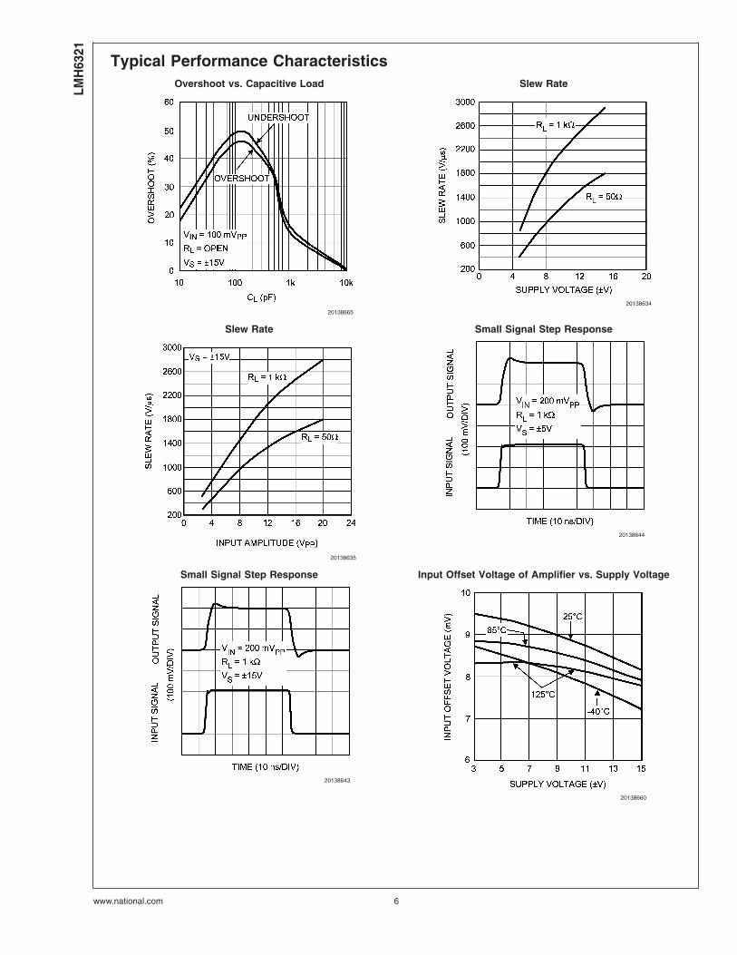
Typical Performance CharacteristicsOvershoot vs. Capacitive Load Slew Rate
20138665
20138634
Slew Rate Small Signal Step Response
20138635
20138644
Small Signal Step Response Input Offset Voltage of Amplifier vs. Supply Voltage
20138643
20138660
LMH
6321
www.national.com 6
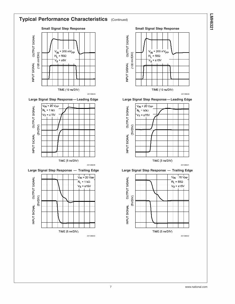
Typical Performance Characteristics (Continued)
Small Signal Step Response Small Signal Step Response
20138645 20138646
Large Signal Step Response — Leading Edge Large Signal Step Response — Leading Edge
20138639 20138641
Large Signal Step Response — Trailing Edge Large Signal Step Response — Trailing Edge
20138640 20138642
LMH
6321
www.national.com7
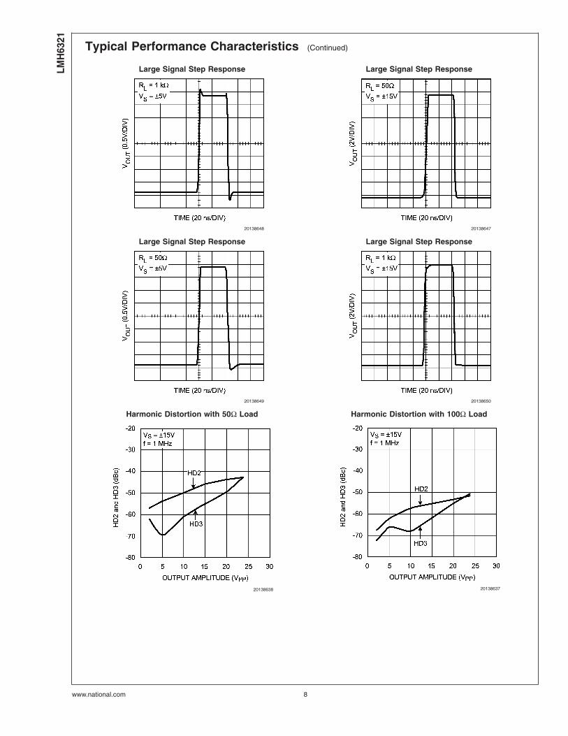
Typical Performance Characteristics (Continued)
Large Signal Step Response Large Signal Step Response
20138648 20138647
Large Signal Step Response Large Signal Step Response
20138649 20138650
Harmonic Distortion with 50Ω Load Harmonic Distortion with 100Ω Load
20138638 20138637
LMH
6321
www.national.com 8
Typical Performance Characteristics (Continued)
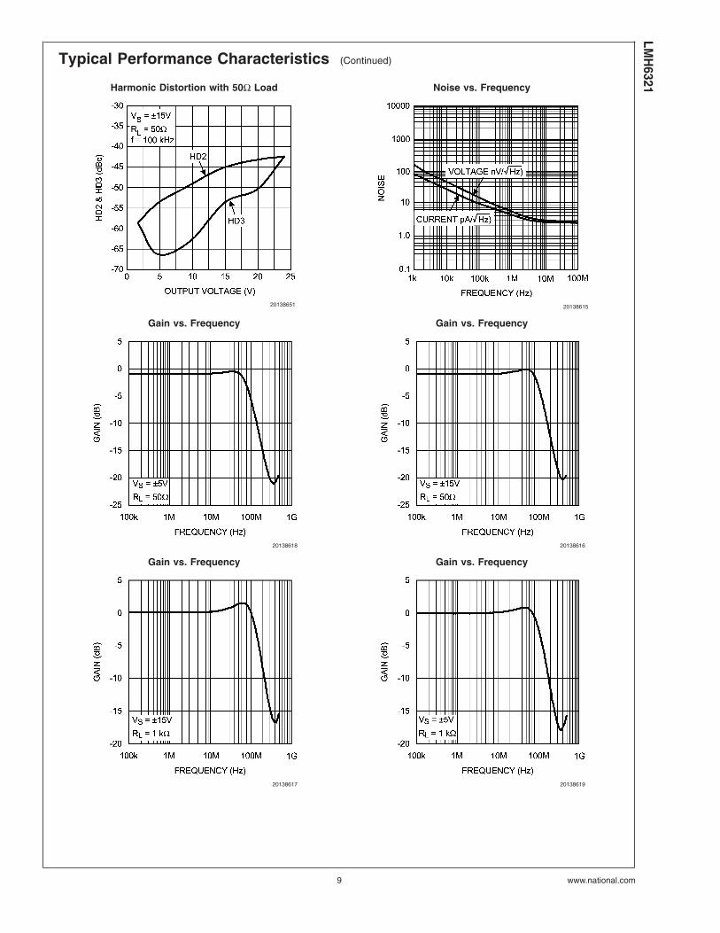
Harmonic Distortion with 50Ω Load Noise vs. Frequency
20138651 20138615
Gain vs. Frequency Gain vs. Frequency
20138618 20138616
Gain vs. Frequency Gain vs. Frequency
20138617 20138619
LMH
6321
www.national.com9
Typical Performance Characteristics (Continued)
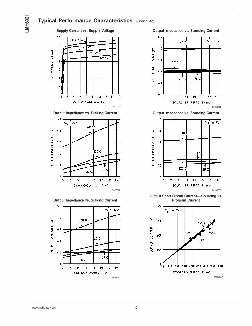
Supply Current vs. Supply Voltage Output Impedance vs. Sourcing Current
20138653 20138654
Output Impedance vs. Sinking Current Output Impedance vs. Sourcing Current
20138620 20138622
Output Impedance vs. Sinking CurrentOutput Short Circuit Current — Sourcing vs.
Program Current
20138621 20138657
LMH
6321
www.national.com 10
Typical Performance Characteristics (Continued)
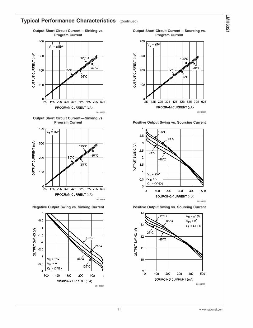
Output Short Circuit Current — Sinking vs.Program Current
Output Short Circuit Current — Sourcing vs.Program Current
20138655 20138661
Output Short Circuit Current — Sinking vs.Program Current Positive Output Swing vs. Sourcing Current
2013865920138623
Negative Output Swing vs. Sinking Current Positive Output Swing vs. Sourcing Current
2013862420138656
LMH
6321
www.national.com11
Typical Performance Characteristics (Continued)
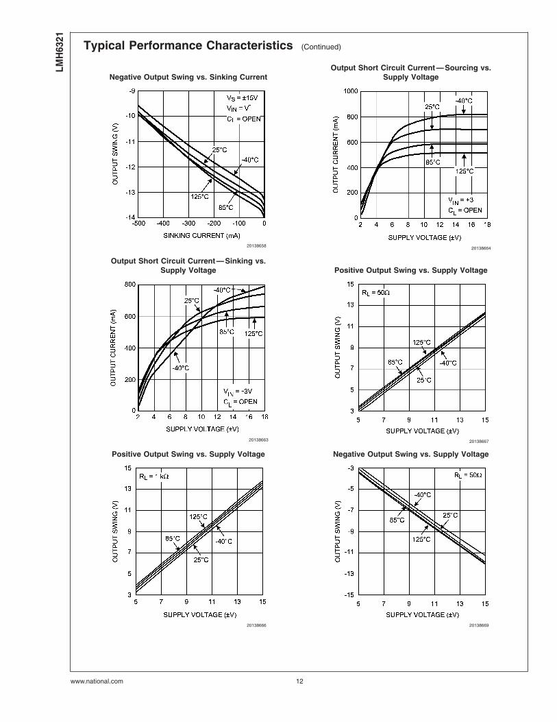
Negative Output Swing vs. Sinking CurrentOutput Short Circuit Current — Sourcing vs.
Supply Voltage
20138658 20138664
Output Short Circuit Current — Sinking vs.Supply Voltage Positive Output Swing vs. Supply Voltage
20138663 20138667
Positive Output Swing vs. Supply Voltage Negative Output Swing vs. Supply Voltage
20138666 20138669
LMH
6321
www.national.com 12
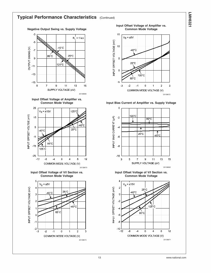
Typical Performance Characteristics (Continued)
Negative Output Swing vs. Supply VoltageInput Offset Voltage of Amplifier vs.
Common Mode Voltage
20138668 20138672
Input Offset Voltage of Amplifier vs.Common Mode Voltage Input Bias Current of Amplifier vs. Supply Voltage
20138670 20138662
Input Offset Voltage of V/I Section vs.Common Mode Voltage
Input Offset Voltage of V/I Section vs.Common Mode Voltage
20138673 20138671
LMH
6321
www.national.com13
Application Hints
BUFFERS
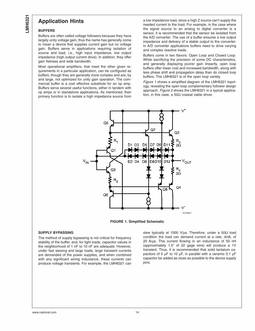
Buffers are often called voltage followers because they havelargely unity voltage gain, thus the name has generally cometo mean a device that supplies current gain but no voltagegain. Buffers serve in applications requiring isolation ofsource and load, i.e., high input impedance, low outputimpedance (high output current drive). In addition, they offergain flatness and wide bandwidth.
Most operational amplifiers, that meet the other given re-quirements in a particular application, can be configured asbuffers, though they are generally more complex and are, byand large, not optimized for unity gain operation. The com-mercial buffer is a cost effective substitute for an op amp.Buffers serve several useful functions, either in tandem withop amps or in standalone applications. As mentioned, theirprimary function is to isolate a high impedance source from
a low impedance load, since a high Z source can’t supply theneeded current to the load. For example, in the case wherethe signal source to an analog to digital converter is asensor, it is recommended that the sensor be isolated fromthe A/D converter. The use of a buffer ensures a low outputimpedance and delivery of a stable output to the converter.In A/D converter applications buffers need to drive varyingand complex reactive loads.
Buffers come in two flavors: Open Loop and Closed Loop.While sacrificing the precision of some DC characteristics,and generally displaying poorer gain linearity, open loopbuffers offer lower cost and increased bandwidth, along withless phase shift and propagation delay than do closed loopbuffers. The LMH6321 is of the open loop variety.
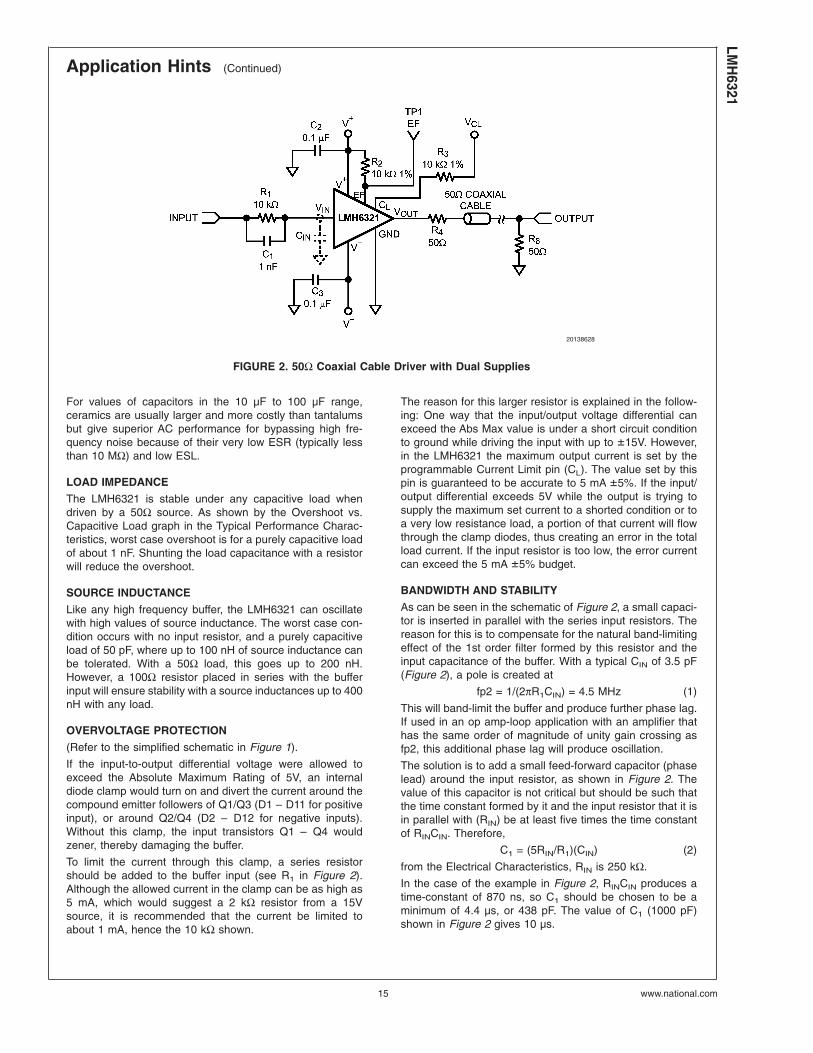
Figure 1 shows a simplified diagram of the LMH6321 topol-ogy, revealing the open loop complementary follower designapproach. Figure 2 shows the LMH6321 in a typical applica-tion, in this case, a 50Ω coaxial cable driver.
SUPPLY BYPASSING
The method of supply bypassing is not critical for frequencystability of the buffer, and, for light loads, capacitor values inthe neighborhood of 1 nF to 10 nF are adequate. However,under fast slewing and large loads, large transient currentsare demanded of the power supplies, and when combinedwith any significant wiring inductance, these currents canproduce voltage transients. For example, the LMH6321 can
slew typically at 1000 V/µs. Therefore, under a 50Ω loadcondition the load can demand current at a rate, di/dt, of20 A/µs. This current flowing in an inductance of 50 nH(approximately 1.5” of 22 gage wire) will produce a 1Vtransient. Thus, it is recommended that solid tantalum ca-pacitors of 5 µF to 10 µF, in parallel with a ceramic 0.1 µFcapacitor be added as close as possible to the device supplypins.
20138627
FIGURE 1. Simplified Schematic
LMH
6321
www.national.com 14
Application Hints (Continued)
For values of capacitors in the 10 µF to 100 µF range,ceramics are usually larger and more costly than tantalumsbut give superior AC performance for bypassing high fre-quency noise because of their very low ESR (typically lessthan 10 MΩ) and low ESL.
LOAD IMPEDANCE
The LMH6321 is stable under any capacitive load whendriven by a 50Ω source. As shown by the Overshoot vs.Capacitive Load graph in the Typical Performance Charac-teristics, worst case overshoot is for a purely capacitive loadof about 1 nF. Shunting the load capacitance with a resistorwill reduce the overshoot.
SOURCE INDUCTANCE
Like any high frequency buffer, the LMH6321 can oscillatewith high values of source inductance. The worst case con-dition occurs with no input resistor, and a purely capacitiveload of 50 pF, where up to 100 nH of source inductance canbe tolerated. With a 50Ω load, this goes up to 200 nH.However, a 100Ω resistor placed in series with the bufferinput will ensure stability with a source inductances up to 400nH with any load.
OVERVOLTAGE PROTECTION
(Refer to the simplified schematic in Figure 1).
If the input-to-output differential voltage were allowed toexceed the Absolute Maximum Rating of 5V, an internaldiode clamp would turn on and divert the current around thecompound emitter followers of Q1/Q3 (D1 – D11 for positiveinput), or around Q2/Q4 (D2 – D12 for negative inputs).Without this clamp, the input transistors Q1 – Q4 wouldzener, thereby damaging the buffer.
To limit the current through this clamp, a series resistorshould be added to the buffer input (see R1 in Figure 2).Although the allowed current in the clamp can be as high as5 mA, which would suggest a 2 kΩ resistor from a 15Vsource, it is recommended that the current be limited toabout 1 mA, hence the 10 kΩ shown.
The reason for this larger resistor is explained in the follow-ing: One way that the input/output voltage differential canexceed the Abs Max value is under a short circuit conditionto ground while driving the input with up to ±15V. However,in the LMH6321 the maximum output current is set by theprogrammable Current Limit pin (CL). The value set by thispin is guaranteed to be accurate to 5 mA ±5%. If the input/output differential exceeds 5V while the output is trying tosupply the maximum set current to a shorted condition or toa very low resistance load, a portion of that current will flowthrough the clamp diodes, thus creating an error in the totalload current. If the input resistor is too low, the error currentcan exceed the 5 mA ±5% budget.
BANDWIDTH AND STABILITY
As can be seen in the schematic of Figure 2, a small capaci-tor is inserted in parallel with the series input resistors. Thereason for this is to compensate for the natural band-limitingeffect of the 1st order filter formed by this resistor and theinput capacitance of the buffer. With a typical CIN of 3.5 pF(Figure 2), a pole is created at
fp2 = 1/(2πR1CIN) = 4.5 MHz (1)
This will band-limit the buffer and produce further phase lag.If used in an op amp-loop application with an amplifier thathas the same order of magnitude of unity gain crossing asfp2, this additional phase lag will produce oscillation.
The solution is to add a small feed-forward capacitor (phaselead) around the input resistor, as shown in Figure 2. Thevalue of this capacitor is not critical but should be such thatthe time constant formed by it and the input resistor that it isin parallel with (RIN) be at least five times the time constantof RINCIN. Therefore,
C1 = (5RIN/R1)(CIN) (2)
from the Electrical Characteristics, RIN is 250 kΩ.
In the case of the example in Figure 2, RINCIN produces atime-constant of 870 ns, so C1 should be chosen to be aminimum of 4.4 µs, or 438 pF. The value of C1 (1000 pF)shown in Figure 2 gives 10 µs.
20138628
FIGURE 2. 50Ω Coaxial Cable Driver with Dual Supplies
LMH
6321
www.national.com15
Application Hints (Continued)
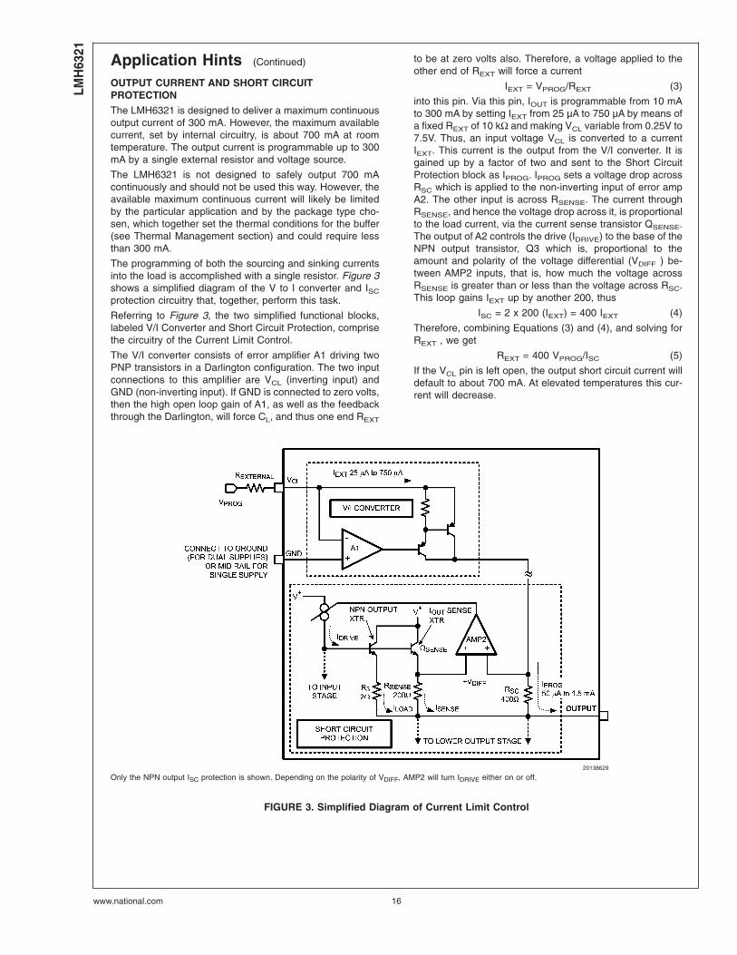
OUTPUT CURRENT AND SHORT CIRCUITPROTECTION
The LMH6321 is designed to deliver a maximum continuousoutput current of 300 mA. However, the maximum availablecurrent, set by internal circuitry, is about 700 mA at roomtemperature. The output current is programmable up to 300mA by a single external resistor and voltage source.
The LMH6321 is not designed to safely output 700 mAcontinuously and should not be used this way. However, theavailable maximum continuous current will likely be limitedby the particular application and by the package type cho-sen, which together set the thermal conditions for the buffer(see Thermal Management section) and could require lessthan 300 mA.
The programming of both the sourcing and sinking currentsinto the load is accomplished with a single resistor. Figure 3shows a simplified diagram of the V to I converter and ISC
protection circuitry that, together, perform this task.
Referring to Figure 3, the two simplified functional blocks,labeled V/I Converter and Short Circuit Protection, comprisethe circuitry of the Current Limit Control.
The V/I converter consists of error amplifier A1 driving twoPNP transistors in a Darlington configuration. The two inputconnections to this amplifier are VCL (inverting input) andGND (non-inverting input). If GND is connected to zero volts,then the high open loop gain of A1, as well as the feedbackthrough the Darlington, will force CL, and thus one end REXT
to be at zero volts also. Therefore, a voltage applied to theother end of REXT will force a current
IEXT = VPROG/REXT (3)
into this pin. Via this pin, IOUT is programmable from 10 mAto 300 mA by setting IEXT from 25 µA to 750 µA by means ofa fixed REXT of 10 kΩ and making VCL variable from 0.25V to7.5V. Thus, an input voltage VCL is converted to a currentIEXT. This current is the output from the V/I converter. It isgained up by a factor of two and sent to the Short CircuitProtection block as IPROG. IPROG sets a voltage drop acrossRSC which is applied to the non-inverting input of error ampA2. The other input is across RSENSE. The current throughRSENSE, and hence the voltage drop across it, is proportionalto the load current, via the current sense transistor QSENSE.The output of A2 controls the drive (IDRIVE) to the base of theNPN output transistor, Q3 which is, proportional to theamount and polarity of the voltage differential (VDIFF ) be-tween AMP2 inputs, that is, how much the voltage acrossRSENSE is greater than or less than the voltage across RSC.This loop gains IEXT up by another 200, thus
ISC = 2 x 200 (IEXT) = 400 IEXT (4)
Therefore, combining Equations (3) and (4), and solving forREXT , we get
REXT = 400 VPROG/ISC (5)
If the VCL pin is left open, the output short circuit current willdefault to about 700 mA. At elevated temperatures this cur-rent will decrease.
20138629
Only the NPN output ISC protection is shown. Depending on the polarity of VDIFF, AMP2 will turn IDRIVE either on or off.
FIGURE 3. Simplified Diagram of Current Limit Control
LMH
6321
www.national.com 16
Application Hints (Continued)
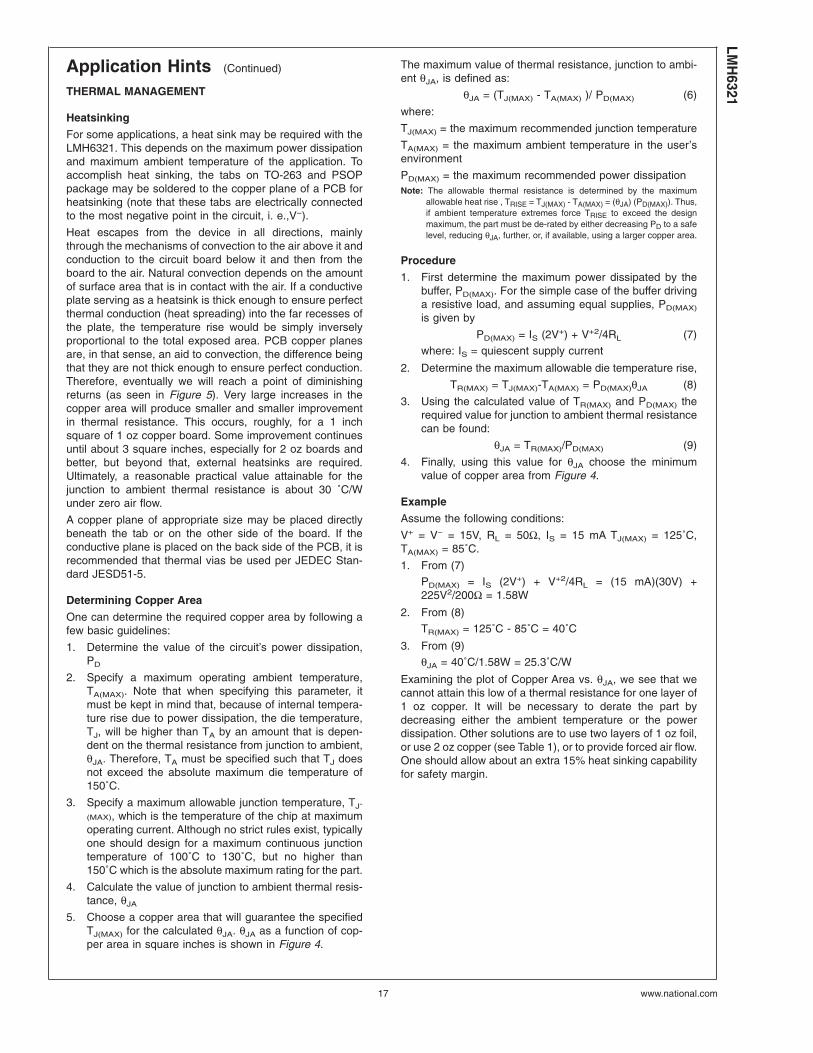
THERMAL MANAGEMENT
Heatsinking
For some applications, a heat sink may be required with theLMH6321. This depends on the maximum power dissipationand maximum ambient temperature of the application. Toaccomplish heat sinking, the tabs on TO-263 and PSOPpackage may be soldered to the copper plane of a PCB forheatsinking (note that these tabs are electrically connectedto the most negative point in the circuit, i. e.,V−).
Heat escapes from the device in all directions, mainlythrough the mechanisms of convection to the air above it andconduction to the circuit board below it and then from theboard to the air. Natural convection depends on the amountof surface area that is in contact with the air. If a conductiveplate serving as a heatsink is thick enough to ensure perfectthermal conduction (heat spreading) into the far recesses ofthe plate, the temperature rise would be simply inverselyproportional to the total exposed area. PCB copper planesare, in that sense, an aid to convection, the difference beingthat they are not thick enough to ensure perfect conduction.Therefore, eventually we will reach a point of diminishingreturns (as seen in Figure 5). Very large increases in thecopper area will produce smaller and smaller improvementin thermal resistance. This occurs, roughly, for a 1 inchsquare of 1 oz copper board. Some improvement continuesuntil about 3 square inches, especially for 2 oz boards andbetter, but beyond that, external heatsinks are required.Ultimately, a reasonable practical value attainable for thejunction to ambient thermal resistance is about 30 ˚C/Wunder zero air flow.
A copper plane of appropriate size may be placed directlybeneath the tab or on the other side of the board. If theconductive plane is placed on the back side of the PCB, it isrecommended that thermal vias be used per JEDEC Stan-dard JESD51-5.
Determining Copper Area
One can determine the required copper area by following afew basic guidelines:
1. Determine the value of the circuit’s power dissipation,PD
2. Specify a maximum operating ambient temperature,TA(MAX). Note that when specifying this parameter, itmust be kept in mind that, because of internal tempera-ture rise due to power dissipation, the die temperature,TJ, will be higher than TA by an amount that is depen-dent on the thermal resistance from junction to ambient,θJA. Therefore, TA must be specified such that TJ doesnot exceed the absolute maximum die temperature of150˚C.
3. Specify a maximum allowable junction temperature, TJ-
(MAX), which is the temperature of the chip at maximumoperating current. Although no strict rules exist, typicallyone should design for a maximum continuous junctiontemperature of 100˚C to 130˚C, but no higher than150˚C which is the absolute maximum rating for the part.
4. Calculate the value of junction to ambient thermal resis-tance, θJA
5. Choose a copper area that will guarantee the specifiedTJ(MAX) for the calculated θJA. θJA as a function of cop-per area in square inches is shown in Figure 4.
The maximum value of thermal resistance, junction to ambi-ent θJA, is defined as:
θJA = (TJ(MAX) - TA(MAX) )/ PD(MAX) (6)
where:
TJ(MAX) = the maximum recommended junction temperature
TA(MAX) = the maximum ambient temperature in the user’senvironment
PD(MAX) = the maximum recommended power dissipationNote: The allowable thermal resistance is determined by the maximum
allowable heat rise , TRISE = TJ(MAX) - TA(MAX) = (θJA) (PD(MAX)). Thus,if ambient temperature extremes force TRISE to exceed the designmaximum, the part must be de-rated by either decreasing PD to a safelevel, reducing θJA, further, or, if available, using a larger copper area.
Procedure
1. First determine the maximum power dissipated by thebuffer, PD(MAX). For the simple case of the buffer drivinga resistive load, and assuming equal supplies, PD(MAX)
is given by
PD(MAX) = IS (2V+) + V+2/4RL (7)
where: IS = quiescent supply current
2. Determine the maximum allowable die temperature rise,
TR(MAX) = TJ(MAX)-TA(MAX) = PD(MAX)θJA (8)
3. Using the calculated value of TR(MAX) and PD(MAX) therequired value for junction to ambient thermal resistancecan be found:
θJA = TR(MAX)/PD(MAX) (9)
4. Finally, using this value for θJA choose the minimumvalue of copper area from Figure 4.
Example
Assume the following conditions:
V+ = V− = 15V, RL = 50Ω, IS = 15 mA TJ(MAX) = 125˚C,TA(MAX) = 85˚C.
1. From (7)
PD(MAX) = IS (2V+) + V+2/4RL = (15 mA)(30V) +225V2/200Ω = 1.58W
2. From (8)
TR(MAX) = 125˚C - 85˚C = 40˚C
3. From (9)
θJA = 40˚C/1.58W = 25.3˚C/W
Examining the plot of Copper Area vs. θJA, we see that wecannot attain this low of a thermal resistance for one layer of1 oz copper. It will be necessary to derate the part bydecreasing either the ambient temperature or the powerdissipation. Other solutions are to use two layers of 1 oz foil,or use 2 oz copper (see Table 1), or to provide forced air flow.One should allow about an extra 15% heat sinking capabilityfor safety margin.
LMH
6321
www.national.com17
Application Hints (Continued)
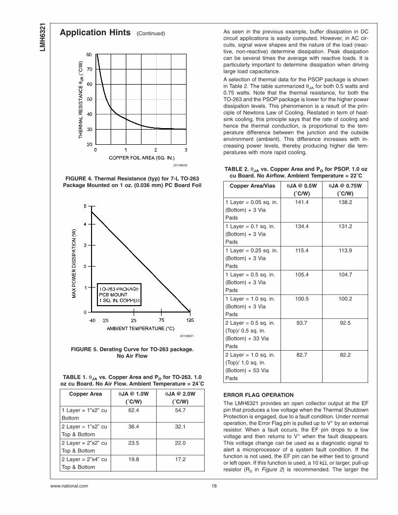
TABLE 1. θJA vs. Copper Area and PD for TO-263. 1.0oz cu Board. No Air Flow. Ambient Temperature = 24˚C
Copper Area θJA @ 1.0W(˚C/W)
θJA @ 2.0W(˚C/W)
1 Layer = 1”x2” cuBottom
62.4 54.7
2 Layer = 1”x2” cuTop & Bottom
36.4 32.1
2 Layer = 2”x2” cuTop & Bottom
23.5 22.0
2 Layer = 2”x4” cuTop & Bottom
19.8 17.2
As seen in the previous example, buffer dissipation in DCcircuit applications is easily computed. However, in AC cir-cuits, signal wave shapes and the nature of the load (reac-tive, non-reactive) determine dissipation. Peak dissipationcan be several times the average with reactive loads. It isparticularly important to determine dissipation when drivinglarge load capacitance.
A selection of thermal data for the PSOP package is shownin Table 2. The table summarized θJA for both 0.5 watts and0.75 watts. Note that the thermal resistance, for both theTO-263 and the PSOP package is lower for the higher powerdissipation levels. This phenomenon is a result of the prin-ciple of Newtons Law of Cooling. Restated in term of heat-sink cooling, this principle says that the rate of cooling andhence the thermal conduction, is proportional to the tem-perature difference between the junction and the outsideenvironment (ambient). This difference increases with in-creasing power levels, thereby producing higher die tem-peratures with more rapid cooling.
TABLE 2. θJA vs. Copper Area and PD for PSOP. 1.0 ozcu Board. No Airflow. Ambient Temperature = 22˚C
Copper Area/Vias θJA @ 0.5W(˚C/W)
θJA @ 0.75W(˚C/W)
1 Layer = 0.05 sq. in.(Bottom) + 3 ViaPads
141.4 138.2
1 Layer = 0.1 sq. in.(Bottom) + 3 ViaPads
134.4 131.2
1 Layer = 0.25 sq. in.(Bottom) + 3 ViaPads
115.4 113.9
1 Layer = 0.5 sq. in.(Bottom) + 3 ViaPads
105.4 104.7
1 Layer = 1.0 sq. in.(Bottom) + 3 ViaPads
100.5 100.2
2 Layer = 0.5 sq. in.(Top)/ 0.5 sq. in.(Bottom) + 33 ViaPads
93.7 92.5
2 Layer = 1.0 sq. in.(Top)/ 1.0 sq. in.(Bottom) + 53 ViaPads
82.7 82.2
ERROR FLAG OPERATION
The LMH6321 provides an open collector output at the EFpin that produces a low voltage when the Thermal ShutdownProtection is engaged, due to a fault condition. Under normaloperation, the Error Flag pin is pulled up to V+ by an externalresistor. When a fault occurs, the EF pin drops to a lowvoltage and then returns to V+ when the fault disappears.This voltage change can be used as a diagnostic signal toalert a microprocessor of a system fault condition. If thefunction is not used, the EF pin can be either tied to groundor left open. If this function is used, a 10 kΩ, or larger, pull-upresistor (R2 in Figure 2) is recommended. The larger the
20138630
FIGURE 4. Thermal Resistance (typ) for 7-L TO-263Package Mounted on 1 oz. (0.036 mm) PC Board Foil
20138631
FIGURE 5. Derating Curve for TO-263 package.No Air Flow
LMH
6321
www.national.com 18
Application Hints (Continued)
resistor the lower the voltage will be at this pin under thermalshutdown. Table 3 shows some typical values of VEF for 10kΩ and 100 kΩ.
TABLE 3. VEF vs. R2 Figure 2
R2 @ V+ = 5V @V+ = 15V
10 kΩ 0.24V 0.55V
100 KΩ 0.036V 0.072V
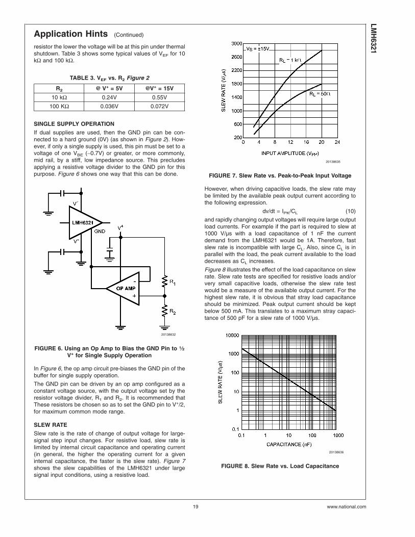
SINGLE SUPPLY OPERATION
If dual supplies are used, then the GND pin can be con-nected to a hard ground (0V) (as shown in Figure 2). How-ever, if only a single supply is used, this pin must be set to avoltage of one VBE (∼0.7V) or greater, or more commonly,mid rail, by a stiff, low impedance source. This precludesapplying a resistive voltage divider to the GND pin for thispurpose. Figure 6 shows one way that this can be done.
In Figure 6, the op amp circuit pre-biases the GND pin of thebuffer for single supply operation.
The GND pin can be driven by an op amp configured as aconstant voltage source, with the output voltage set by theresistor voltage divider, R1 and R2. It is recommended thatThese resistors be chosen so as to set the GND pin to V+/2,for maximum common mode range.
SLEW RATE
Slew rate is the rate of change of output voltage for large-signal step input changes. For resistive load, slew rate islimited by internal circuit capacitance and operating current(in general, the higher the operating current for a giveninternal capacitance, the faster is the slew rate). Figure 7shows the slew capabilities of the LMH6321 under largesignal input conditions, using a resistive load.
However, when driving capacitive loads, the slew rate maybe limited by the available peak output current according tothe following expression.
dv/dt = IPK/CL (10)
and rapidly changing output voltages will require large outputload currents. For example if the part is required to slew at1000 V/µs with a load capacitance of 1 nF the currentdemand from the LMH6321 would be 1A. Therefore, fastslew rate is incompatible with large CL. Also, since CL is inparallel with the load, the peak current available to the loaddecreases as CL increases.
Figure 8 illustrates the effect of the load capacitance on slewrate. Slew rate tests are specified for resistive loads and/orvery small capacitive loads, otherwise the slew rate testwould be a measure of the available output current. For thehighest slew rate, it is obvious that stray load capacitanceshould be minimized. Peak output current should be keptbelow 500 mA. This translates to a maximum stray capaci-tance of 500 pF for a slew rate of 1000 V/µs.
20138632
FIGURE 6. Using an Op Amp to Bias the GND Pin to 1⁄2V+ for Single Supply Operation
20138635
FIGURE 7. Slew Rate vs. Peak-to-Peak Input Voltage
20138636
FIGURE 8. Slew Rate vs. Load Capacitance
LMH
6321
www.national.com19
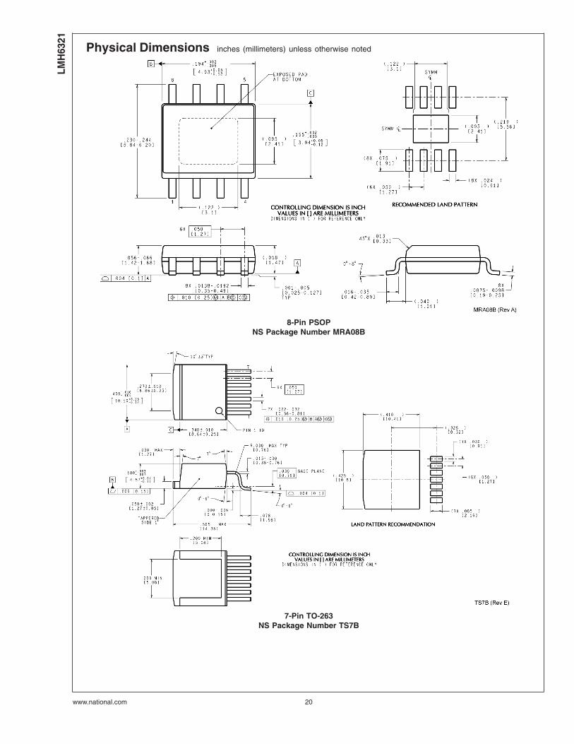
Physical Dimensions inches (millimeters) unless otherwise noted
8-Pin PSOPNS Package Number MRA08B
7-Pin TO-263NS Package Number TS7B
LMH
6321
www.national.com 20
Notes
National does not assume any responsibility for use of any circuitry described, no circuit patent licenses are implied and National reservesthe right at any time without notice to change said circuitry and specifications.
For the most current product information visit us at www.national.com.
LIFE SUPPORT POLICY
NATIONAL’S PRODUCTS ARE NOT AUTHORIZED FOR USE AS CRITICAL COMPONENTS IN LIFE SUPPORT DEVICES OR SYSTEMSWITHOUT THE EXPRESS WRITTEN APPROVAL OF THE PRESIDENT AND GENERAL COUNSEL OF NATIONAL SEMICONDUCTORCORPORATION. As used herein:
1. Life support devices or systems are devices or systemswhich, (a) are intended for surgical implant into the body, or(b) support or sustain life, and whose failure to perform whenproperly used in accordance with instructions for useprovided in the labeling, can be reasonably expected to resultin a significant injury to the user.
2. A critical component is any component of a life supportdevice or system whose failure to perform can be reasonablyexpected to cause the failure of the life support device orsystem, or to affect its safety or effectiveness.
BANNED SUBSTANCE COMPLIANCE
National Semiconductor follows the provisions of the Product Stewardship Guide for Customers (CSP-9-111C2) and Banned Substancesand Materials of Interest Specification (CSP-9-111S2) for regulatory environmental compliance. Details may be found at:www.national.com/quality/green.
Lead free products are RoHS compliant.
National SemiconductorAmericas CustomerSupport CenterEmail: [email protected]: 1-800-272-9959
National SemiconductorEurope Customer Support Center
Fax: +49 (0) 180-530 85 86Email: [email protected]
Deutsch Tel: +49 (0) 69 9508 6208English Tel: +44 (0) 870 24 0 2171Français Tel: +33 (0) 1 41 91 8790
National SemiconductorAsia Pacific CustomerSupport CenterEmail: [email protected]
National SemiconductorJapan Customer Support CenterFax: 81-3-5639-7507Email: [email protected]: 81-3-5639-7560
www.national.com
LMH
6321300
mA
High
Speed
Buffer
with
Adjustable
Current
Limit