Embed Size (px)
Citation preview
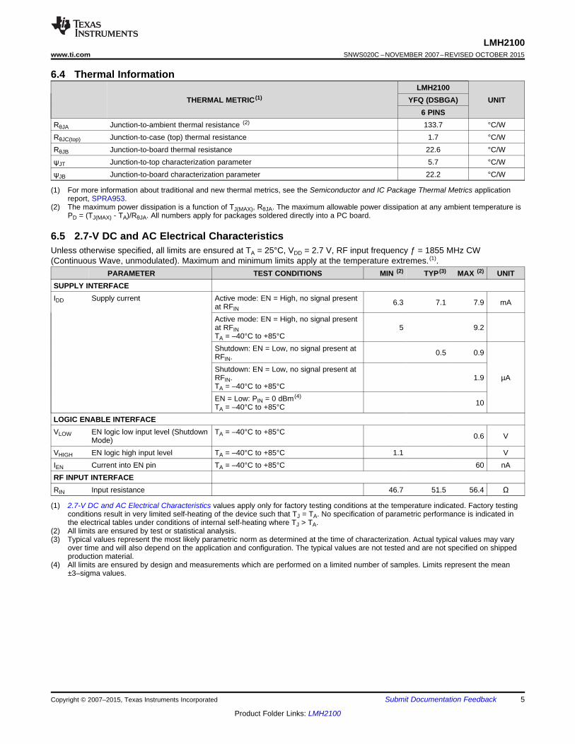
PAANTENNA
RFIN OUT
LMH2100
RF
VDD
GND
50 :
REF
ADC
2
CPRP
1 6
34 5 -
+
COUPLER
EN
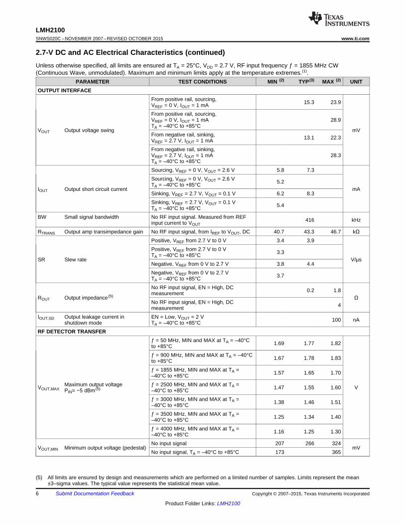
PAANTENNA
RFIN OUT
LMH2100
RF
VDD
GND
50 :
EN REF
ADC
2
CS
RS
1 6
34 5 -
+
COUPLER
Product
Folder
Sample &Buy
Technical
Documents
Tools &
Software
Support &Community
LMH2100SNWS020C –NOVEMBER 2007–REVISED OCTOBER 2015
LMH2100 50-MHz to 4-GHz 40-dB Logarithmic Power Detector for CDMA and WCDMA1 Features 3 Description
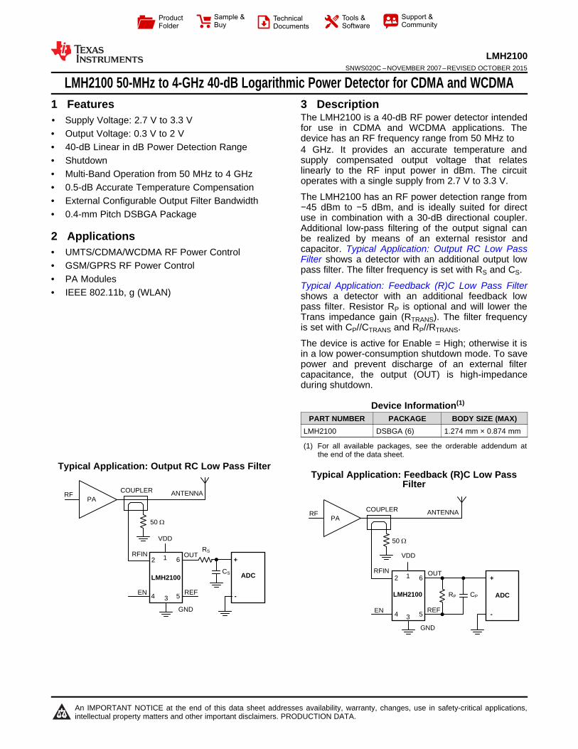
The LMH2100 is a 40-dB RF power detector intended1• Supply Voltage: 2.7 V to 3.3 V
for use in CDMA and WCDMA applications. The• Output Voltage: 0.3 V to 2 V device has an RF frequency range from 50 MHz to• 40-dB Linear in dB Power Detection Range 4 GHz. It provides an accurate temperature and
supply compensated output voltage that relates• Shutdownlinearly to the RF input power in dBm. The circuit• Multi-Band Operation from 50 MHz to 4 GHzoperates with a single supply from 2.7 V to 3.3 V.
• 0.5-dB Accurate Temperature CompensationThe LMH2100 has an RF power detection range from• External Configurable Output Filter Bandwidth−45 dBm to −5 dBm, and is ideally suited for direct
• 0.4-mm Pitch DSBGA Package use in combination with a 30-dB directional coupler.Additional low-pass filtering of the output signal can
2 Applications be realized by means of an external resistor andcapacitor. Typical Application: Output RC Low Pass• UMTS/CDMA/WCDMA RF Power ControlFilter shows a detector with an additional output low
• GSM/GPRS RF Power Control pass filter. The filter frequency is set with RS and CS.• PA Modules
Typical Application: Feedback (R)C Low Pass Filter• IEEE 802.11b, g (WLAN) shows a detector with an additional feedback low
pass filter. Resistor RP is optional and will lower theTrans impedance gain (RTRANS). The filter frequencyis set with CP//CTRANS and RP//RTRANS.
The device is active for Enable = High; otherwise it isin a low power-consumption shutdown mode. To savepower and prevent discharge of an external filtercapacitance, the output (OUT) is high-impedanceduring shutdown.
Device Information(1)
PART NUMBER PACKAGE BODY SIZE (MAX)LMH2100 DSBGA (6) 1.274 mm × 0.874 mm
(1) For all available packages, see the orderable addendum atthe end of the data sheet.
Typical Application: Output RC Low Pass FilterTypical Application: Feedback (R)C Low Pass
Filter
1
An IMPORTANT NOTICE at the end of this data sheet addresses availability, warranty, changes, use in safety-critical applications,intellectual property matters and other important disclaimers. PRODUCTION DATA.
LMH2100SNWS020C –NOVEMBER 2007–REVISED OCTOBER 2015 www.ti.com
Table of Contents7.3 Feature Description................................................. 231 Features .................................................................. 17.4 Device Functional Modes........................................ 292 Applications ........................................................... 1
8 Application and Implementation ........................ 303 Description ............................................................. 18.1 Application Information............................................ 304 Revision History..................................................... 28.2 Typical Applications ............................................... 335 Pin Configuration and Functions ......................... 3
9 Power Supply Recommendations ...................... 396 Specifications......................................................... 410 Layout................................................................... 406.1 Absolute Maximum Ratings ..................................... 4
10.1 Layout Guidelines ................................................ 406.2 ESD Ratings.............................................................. 410.2 Layout Example .................................................... 426.3 Recommended Operating Ratings ........................... 4
11 Device and Documentation Support ................. 436.4 Thermal Information .................................................. 511.1 Community Resources.......................................... 436.5 2.7-V DC and AC Electrical Characteristics.............. 511.2 Trademarks ........................................................... 436.6 Timing Requirements .............................................. 1111.3 Electrostatic Discharge Caution............................ 436.7 Typical Characteristics ............................................ 1111.4 Glossary ................................................................ 437 Detailed Description ............................................ 23
12 Mechanical, Packaging, and Orderable7.1 Overview ................................................................. 23Information ........................................................... 437.2 Functional Block Diagram ....................................... 23
4 Revision HistoryNOTE: Page numbers for previous revisions may differ from page numbers in the current version.
Changes from Revision B (March 2013) to Revision C Page
• Added Device Information and Pin Configuration and Functions sections, ESD Ratings table, Feature Description,Device Functional Modes, Application and Implementation, Power Supply Recommendations, Layout, Device andDocumentation Support, and Mechanical, Packaging, and Orderable Information sections. ................................................ 1
Changes from Revision A (March 2013) to Revision B Page
• Changed layout of National Data Sheet to TI format ........................................................................................................... 42
2 Submit Documentation Feedback Copyright © 2007–2015, Texas Instruments Incorporated
Product Folder Links: LMH2100
A1VDD
B1RFIN
C2EN
B2REF
A2OUT
C1GND
LMH2100www.ti.com SNWS020C –NOVEMBER 2007–REVISED OCTOBER 2015
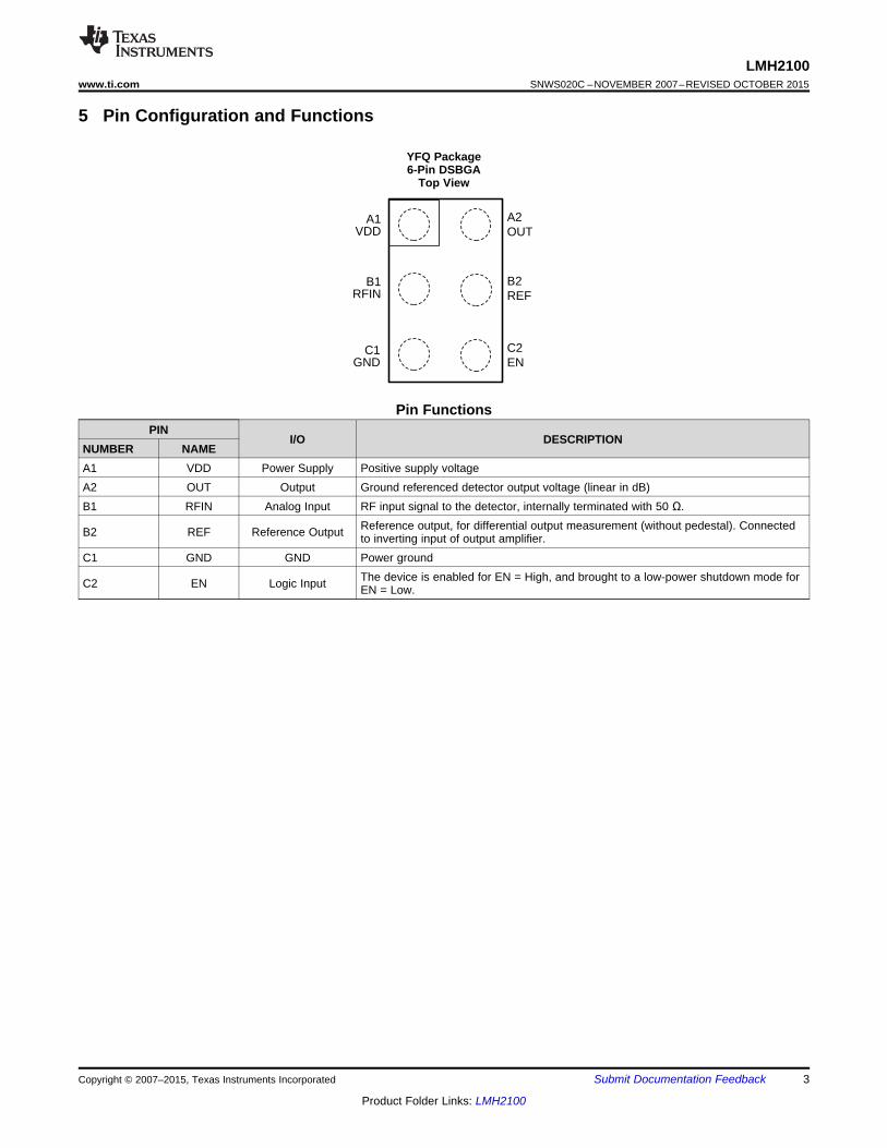
5 Pin Configuration and Functions
YFQ Package6-Pin DSBGA
Top View
Pin FunctionsPIN
I/O DESCRIPTIONNUMBER NAMEA1 VDD Power Supply Positive supply voltageA2 OUT Output Ground referenced detector output voltage (linear in dB)B1 RFIN Analog Input RF input signal to the detector, internally terminated with 50 Ω.
Reference output, for differential output measurement (without pedestal). ConnectedB2 REF Reference Output to inverting input of output amplifier.C1 GND GND Power ground
The device is enabled for EN = High, and brought to a low-power shutdown mode forC2 EN Logic Input EN = Low.
Copyright © 2007–2015, Texas Instruments Incorporated Submit Documentation Feedback 3
Product Folder Links: LMH2100
LMH2100SNWS020C –NOVEMBER 2007–REVISED OCTOBER 2015 www.ti.com
6 Specifications
6.1 Absolute Maximum Ratingsover operating free-air temperature range (unless otherwise noted) (1) (2)
MIN MAX UNITSupply voltage, VDD to GND 3.6 VRF input, input power 10 dBmRF input, DC voltage 400 mVEnable input voltage VSS – 0.4 < VEN < VDD + 0.4 VJunction temperature (3) 150 °CMaximum lead temperature (soldering,10 sec) 260 °CStorage temperature, Tstg −65 150 °C
(1) Stresses beyond those listed under Absolute Maximum Ratings may cause permanent damage to the device. These are stress ratingsonly, which do not imply functional operation of the device at these or any other conditions beyond those indicated under RecommendedOperating Conditions. Exposure to absolute-maximum-rated conditions for extended periods may affect device reliability. For ensuredspecifications and the test conditions, see the 2.7-V DC and AC Electrical Characteristics.
(2) If Military/Aerospace specified devices are required, contact the Texas Instruments Sales Office/ Distributors for availability andspecifications.
(3) The maximum power dissipation is a function of TJ(MAX), RθJA. The maximum allowable power dissipation at any ambient temperature isPD = (TJ(MAX) – TA)/RθJA. All numbers apply for packages soldered directly into a PC board.
6.2 ESD RatingsVALUE UNIT
Human-body model (HBM), per ANSI/ESDA/JEDEC JS-001 (1) ±2000V(ESD) Electrostatic discharge Charged-device model (CDM), per JEDEC specification JESD22-C101 (2) ±2000 V
Machine model ±200
(1) JEDEC document JEP155 states that 500-V HBM allows safe manufacturing with a standard ESD control process.(2) JEDEC document JEP157 states that 250-V CDM allows safe manufacturing with a standard ESD control process.
6.3 Recommended Operating Ratingsover operating free-air temperature range (unless otherwise noted) (1)
MIN NOM MAX UNITSupply voltage 2.7 3.3 VTemperature range –40 85 °CRF frequency range 50 4000 MHz
–45 –5 dBmRF input power range (2)–58 –18 dBV
(1) Stresses beyond those listed under Absolute Maximum Ratings may cause permanent damage to the device. These are stress ratingsonly, which do not imply functional operation of the device at these or any other conditions beyond those indicated under RecommendedOperating Conditions. Exposure to absolute-maximum-rated conditions for extended periods may affect device reliability. For ensuredspecifications and the test conditions, see the 2.7-V DC and AC Electrical Characteristics.
(2) Power in dBV = dBm + 13 when the impedance is 50 Ω.
4 Submit Documentation Feedback Copyright © 2007–2015, Texas Instruments Incorporated
Product Folder Links: LMH2100
LMH2100www.ti.com SNWS020C –NOVEMBER 2007–REVISED OCTOBER 2015
6.4 Thermal InformationLMH2100
THERMAL METRIC (1) YFQ (DSBGA) UNIT6 PINS
RθJA Junction-to-ambient thermal resistance (2) 133.7 °C/WRθJC(top) Junction-to-case (top) thermal resistance 1.7 °C/WRθJB Junction-to-board thermal resistance 22.6 °C/WψJT Junction-to-top characterization parameter 5.7 °C/WψJB Junction-to-board characterization parameter 22.2 °C/W
(1) For more information about traditional and new thermal metrics, see the Semiconductor and IC Package Thermal Metrics applicationreport, SPRA953.
(2) The maximum power dissipation is a function of TJ(MAX), RθJA. The maximum allowable power dissipation at any ambient temperature isPD = (TJ(MAX) - TA)/RθJA. All numbers apply for packages soldered directly into a PC board.
6.5 2.7-V DC and AC Electrical CharacteristicsUnless otherwise specified, all limits are ensured at TA = 25°C, VDD = 2.7 V, RF input frequency ƒ = 1855 MHz CW(Continuous Wave, unmodulated). Maximum and minimum limits apply at the temperature extremes. (1).
PARAMETER TEST CONDITIONS MIN (2) TYP (3) MAX (2) UNITSUPPLY INTERFACEIDD Supply current Active mode: EN = High, no signal present 6.3 7.1 7.9 mAat RFIN
Active mode: EN = High, no signal presentat RFIN 5 9.2TA = –40°C to +85°CShutdown: EN = Low, no signal present at 0.5 0.9RFIN.Shutdown: EN = Low, no signal present atRFIN. 1.9 µATA = –40°C to +85°CEN = Low: PIN = 0 dBm (4)
10TA = –40°C to +85°CLOGIC ENABLE INTERFACEVLOW EN logic low input level (Shutdown TA = –40°C to +85°C 0.6 VMode)VHIGH EN logic high input level TA = –40°C to +85°C 1.1 VIEN Current into EN pin TA = –40°C to +85°C 60 nARF INPUT INTERFACERIN Input resistance 46.7 51.5 56.4 Ω
(1) 2.7-V DC and AC Electrical Characteristics values apply only for factory testing conditions at the temperature indicated. Factory testingconditions result in very limited self-heating of the device such that TJ = TA. No specification of parametric performance is indicated inthe electrical tables under conditions of internal self-heating where TJ > TA.
(2) All limits are ensured by test or statistical analysis.(3) Typical values represent the most likely parametric norm as determined at the time of characterization. Actual typical values may vary
over time and will also depend on the application and configuration. The typical values are not tested and are not specified on shippedproduction material.
(4) All limits are ensured by design and measurements which are performed on a limited number of samples. Limits represent the mean±3–sigma values.
Copyright © 2007–2015, Texas Instruments Incorporated Submit Documentation Feedback 5
Product Folder Links: LMH2100
LMH2100SNWS020C –NOVEMBER 2007–REVISED OCTOBER 2015 www.ti.com
2.7-V DC and AC Electrical Characteristics (continued)Unless otherwise specified, all limits are ensured at TA = 25°C, VDD = 2.7 V, RF input frequency ƒ = 1855 MHz CW(Continuous Wave, unmodulated). Maximum and minimum limits apply at the temperature extremes.(1).
PARAMETER TEST CONDITIONS MIN (2) TYP (3) MAX (2) UNITOUTPUT INTERFACE
From positive rail, sourcing, 15.3 23.9VREF = 0 V, IOUT = 1 mAFrom positive rail, sourcing,VREF = 0 V, IOUT = 1 mA 28.9TA = –40°C to +85°C
VOUT Output voltage swing mVFrom negative rail, sinking, 13.1 22.3VREF = 2.7 V, IOUT = 1 mAFrom negative rail, sinking,VREF = 2.7 V, IOUT = 1 mA 28.3TA = –40°C to +85°CSourcing, VREF = 0 V, VOUT = 2.6 V 5.8 7.3Sourcing, VREF = 0 V, VOUT = 2.6 V 5.2TA = –40°C to +85°C
IOUT Output short circuit current mASinking, VREF = 2.7 V, VOUT = 0.1 V 6.2 8.3Sinking, VREF = 2.7 V, VOUT = 0.1 V 5.4TA = –40°C to +85°C
BW Small signal bandwidth No RF input signal. Measured from REF 416 kHzinput current to VOUT
RTRANS Output amp transimpedance gain No RF input signal, from IREF to VOUT, DC 40.7 43.3 46.7 kΩPositive, VREF from 2.7 V to 0 V 3.4 3.9Positive, VREF from 2.7 V to 0 V 3.3TA = –40°C to +85°C
SR Slew rate V/µsNegative, VREF from 0 V to 2.7 V 3.8 4.4Negative, VREF from 0 V to 2.7 V 3.7TA = –40°C to +85°CNo RF input signal, EN = High, DC 0.2 1.8measurement
ROUT Output impedance (5) ΩNo RF input signal, EN = High, DC 4measurement
IOUT,SD Output leakage current in EN = Low, VOUT = 2 V 100 nAshutdown mode TA = –40°C to +85°CRF DETECTOR TRANSFER
ƒ = 50 MHz, MIN and MAX at TA = –40°C 1.69 1.77 1.82to +85°Cƒ = 900 MHz, MIN and MAX at TA = –40°C 1.67 1.78 1.83to +85°Cƒ = 1855 MHz, MIN and MAX at TA = 1.57 1.65 1.70–40°C to +85°C
Maximum output voltage ƒ = 2500 MHz, MIN and MAX at TA =VOUT,MAX 1.47 1.55 1.60 VPIN= −5 dBm (5) –40°C to +85°Cƒ = 3000 MHz, MIN and MAX at TA = 1.38 1.46 1.51–40°C to +85°Cƒ = 3500 MHz, MIN and MAX at TA = 1.25 1.34 1.40–40°C to +85°Cƒ = 4000 MHz, MIN and MAX at TA = 1.16 1.25 1.30–40°C to +85°CNo input signal 207 266 324
VOUT,MIN Minimum output voltage (pedestal) mVNo input signal, TA = –40°C to +85°C 173 365
(5) All limits are ensured by design and measurements which are performed on a limited number of samples. Limits represent the mean±3–sigma values. The typical value represents the statistical mean value.
6 Submit Documentation Feedback Copyright © 2007–2015, Texas Instruments Incorporated
Product Folder Links: LMH2100
LMH2100www.ti.com SNWS020C –NOVEMBER 2007–REVISED OCTOBER 2015
2.7-V DC and AC Electrical Characteristics (continued)Unless otherwise specified, all limits are ensured at TA = 25°C, VDD = 2.7 V, RF input frequency ƒ = 1855 MHz CW(Continuous Wave, unmodulated). Maximum and minimum limits apply at the temperature extremes.(1).
PARAMETER TEST CONDITIONS MIN (2) TYP (3) MAX (2) UNITƒ = 50 MHz, MIN and MAX at TA = –40°C 1.38 1.44 1.49to +85°Cƒ = 900 MHz, MIN and MAX at TA = –40°C 1.34 1.43 1.46to +85°Cƒ = 1855 MHz, MIN and MAX at TA = 1.27 1.32 1.36–40°C to +85°C
Output voltage range ƒ = 2500 MHz, MIN and MAX at TA =ΔVOUT 1.19 1.23 1.27 VPIN from −45 dBm to −5 dBm (5) –40°C to +85°Cƒ = 3000 MHz, MIN and MAX at TA = 1.11 1.16 1.19–40°C to +85°Cƒ = 3500 MHz, MIN and MAX at TA = 1 1.05 1.1–40°C to +85°Cƒ = 4000 MHz, MIN and MAX at TA = 0.91 0.97 1.01–40°C to +85°Cƒ = 50 MHz 39.6 40.9 42.1ƒ = 900 MHz 37.0 38.2 39.4ƒ = 1855 MHz 34.5 35.5 36.5
KSLOPE Logarithmic slope (5) ƒ = 2500 MHz 32.7 33.7 34.6 mV/dBƒ = 3000 MHz 31.1 32.1 33.1ƒ = 3500 MHz 29.7 30.7 31.6f = 4000 MHz 28.5 29.4 30.3ƒ = 50 MHz –50.2 −49.5 –48.8ƒ = 900 MHz –53.6 −52.7 –51.8ƒ = 1855 MHz –53.2 −52.3 –51.4
PINT Logarithmic intercept (5) ƒ = 2500 MHz –52.4 −51.2 –50.1 dBmƒ = 3000 MHz –51.2 −50.1 –48.9ƒ = 3500 MHz –49.1 −47.8 –46.4ƒ = 4000 MHz –47.3 −46.1 –44.9
en Output referred noise (6) PIN = −10 dBm at 10 kHz 1.5 µV/√HzvN Output referred noise (5) Integrated over frequency band, 1 kHz to 1006.5 kHz
µVRMSIntegrated over frequency band, 1 kHz to6.5 kHz 150TA = –40°C to +85°CPIN = −10 dBm, ƒ = 1800 MHz 60
PSRR Power supply rejection ratio (6) dBPIN = −10 dBm, ƒ = 1800 MHz 55TA = –40°C to +85°C
(6) This parameter is ensured by design and/or characterization and is not tested in production.
Copyright © 2007–2015, Texas Instruments Incorporated Submit Documentation Feedback 7
Product Folder Links: LMH2100
LMH2100SNWS020C –NOVEMBER 2007–REVISED OCTOBER 2015 www.ti.com
2.7-V DC and AC Electrical Characteristics (continued)Unless otherwise specified, all limits are ensured at TA = 25°C, VDD = 2.7 V, RF input frequency ƒ = 1855 MHz CW(Continuous Wave, unmodulated). Maximum and minimum limits apply at the temperature extremes.(1).
PARAMETER TEST CONDITIONS MIN (2) TYP (3) MAX (2) UNITPOWER MEASUREMENT PERFORMANCE
ƒ = 50 MHz –0.2 0.12 1.2ƒ = 50 MHz, MIN and MAX at TA = –40°C –0.8 1.3to +85°Cƒ = 900 MHz –0.4 –0.06 0.2ƒ = 900 MHz, MIN and MAX at TA = –40°C –1 0.3to +85°Cƒ = 1855 MHz –0.3 -0.03 0.3ƒ = 1855 MHz, MIN and MAX at TA = –0.7 0.4–40°C to +85°Cƒ = 2500 MHz –0.2 0.04 0.8
Log conformance error (5)ELC dBƒ = 2500 MHz, MIN and MAX at TA =−40 dBm ≤ PIN ≤ −10 dBm –0.8 1.1–40°C to +85°C
ƒ = 3000 MHz –0.1 0.13 1.6ƒ = 3000 MHz, MIN and MAX at TA = 1 1.8–40°C to +85°Cƒ = 3500 MHz -0.036 0.35 3.3ƒ = 3500 MHz, MIN and MAX at TA = –1 3.5–40°C to +85°Cƒ = 4000 MHz –0.048 0.65 4.6ƒ = 4000 MHz, MIN and MAX at TA = –1 4.9–40°C to +85°Cƒ = 50 MHz, MIN and MAX at TA = –40°C –0.63 0.43to +85°Cƒ = 900 MHz, MIN and MAX at TA = –40°C –0.94 0.30to +85°Cƒ = 1855 MHz, MIN and MAX at TA = –0.71 0.33–40°C to +85°C
Variation over temperature (5) ƒ = 2500 MHz, MIN and MAX at TA =EVOT –0.88 0.35 dB−40 dBm ≤ PIN ≤ −10 dBm –40°C to +85°Cƒ = 3000 MHz, MIN and MAX at TA = –1.03 0.37–40°C to +85°Cƒ = 3500 MHz, MIN and MAX at TA = –1.10 0.33–40°C to +85°Cƒ = 4000 MHz, MIN and MAX at TA = –1.12 0.33–40°C to +85°Cƒ = 50 MHz, MIN and MAX at TA = –40°C –0.064 0.066to +85°Cƒ = 900 MHz, MIN and MAX at TA = –40°C –0.123 0.051to +85°Cƒ = 1855 MHz, MIN and MAX at TA = –0.050 0.067–40°C to +85°C
Measurement Error for a 1-dB ƒ = 2500 MHz, MIN and MAX at TA =E1 dB Input power step (5) –0.058 0.074 dB–40°C to +85°C−40 dBm ≤ PIN ≤ −10 dBmƒ = 3000 MHz, MIN and MAX at TA = –0.066 0.069–40°C to +85°Cƒ = 3500 MHz, MIN and MAX at TA = –0.082 0.066–40°C to +85°Cƒ = 4000 MHz, MIN and MAX at TA = –0.098 0.072–40°C to +85°C
8 Submit Documentation Feedback Copyright © 2007–2015, Texas Instruments Incorporated
Product Folder Links: LMH2100

LMH2100www.ti.com SNWS020C –NOVEMBER 2007–REVISED OCTOBER 2015
2.7-V DC and AC Electrical Characteristics (continued)Unless otherwise specified, all limits are ensured at TA = 25°C, VDD = 2.7 V, RF input frequency ƒ = 1855 MHz CW(Continuous Wave, unmodulated). Maximum and minimum limits apply at the temperature extremes.(1).
PARAMETER TEST CONDITIONS MIN (2) TYP (3) MAX (2) UNITƒ = 50 MHz, MIN and MAX at TA = –40°C –0.40 0.27to +85°Cƒ = 900 MHz, MIN and MAX at TA = –40°C –0.58 0.22to +85°Cƒ = 1855 MHz, MIN and MAX at TA = –0.29 0.20–40°C to +85°C
Measurement Error for a 10-dB ƒ = 2500 MHz, MIN and MAX at TA =E10 dB Input power step (5) –0.28 0.24 dB–40°C to +85°C−40 dBm ≤ PIN ≤ −10 dBmƒ = 3000 MHz, MIN and MAX at TA = –0.38 0.29–40°C to +85°Cƒ = 3500 MHz, MIN and MAX at TA = –0.60 0.40–40°C to +85°Cƒ = 4000 MHz, MIN and MAX at TA = –0.82 0.43–40°C to +85°Cƒ = 50 MHz, MIN and MAX at TA = –40°C –6.5 8.6to +85°Cƒ = 900 MHz, MIN and MAX at TA = –40°C –4.7 14.5to +85°Cƒ = 1855 MHz, MIN and MAX at TA = –5.1 11.0–40°C to +85°C
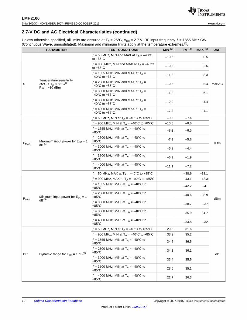
Temperature sensitivity ƒ = 2500 MHz, MIN and MAX at TA =ST –40°C < TA < 25°C –4.3 13.6 mdB/°C–40°C to +85°C−40 dBm ≤ PIN ≤ −10 dBm (5)
ƒ = 3000 MHz, MIN and MAX at TA = –1.5 15.8–40°C to +85°Cƒ = 3500 MHz, MIN and MAX at TA = 0.1 16.9–40°C to +85°Cƒ = 4000 MHz, MIN and MAX at TA = 0.5 17.3–40°C to +85°Cƒ = 50 MHz, MIN at TA = –40°C to +85°C –10.5 0.5ƒ = 900 MHz, MIN at TA = –40°C to +85°C –10.5 2.6ƒ = 1855 MHz, MIN at TA = –40°C to –11.3 3.4+85°Cƒ = 2500 MHz, MIN at TA = –40°C toTemperature sensitivity –10.6 5.8+85°CST 25°C < TA < 85°C mdB/°Cƒ = 3000 MHz, MIN at TA = –40°C to−40 dBm ≤ PIN ≤ −10 dBm (5)
–11.2 6.1+85°Cƒ = 3500 MHz, MIN at TA = –40°C to –12.9 5.5+85°Cƒ = 4000 MHz, MIN at TA = –40°C to –17.8 5.5+85°Cƒ = 50 MHz, MAX at TA = –40°C to +85°C –5.4 8.6ƒ = 900 MHz, MAX at TA = –40°C to +85°C 0.3 14.5ƒ = 1855 MHz, MAX at TA = –40°C to –3.1 11.0+85°Cƒ = 2500 MHz, MAX at TA = –40°C toTemperature sensitivity –1.6 13.6+85°CST −40°C < TA < 25°C (5) mdB/°Cƒ = 3000 MHz, MAX at TA = –40°C toPIN = −10 dBm 0.9 15.8+85°Cƒ = 3500 MHz, MAX at TA = –40°C to 2.5 16.9+85°Cƒ = 4000 MHz, MAX at TA = –40°C to 2.7 17.3+85°C
Copyright © 2007–2015, Texas Instruments Incorporated Submit Documentation Feedback 9
Product Folder Links: LMH2100
LMH2100SNWS020C –NOVEMBER 2007–REVISED OCTOBER 2015 www.ti.com
2.7-V DC and AC Electrical Characteristics (continued)Unless otherwise specified, all limits are ensured at TA = 25°C, VDD = 2.7 V, RF input frequency ƒ = 1855 MHz CW(Continuous Wave, unmodulated). Maximum and minimum limits apply at the temperature extremes.(1).
PARAMETER TEST CONDITIONS MIN (2) TYP (3) MAX (2) UNITƒ = 50 MHz, MIN and MAX at TA = –40°C –10.5 0.5to +85°Cƒ = 900 MHz, MIN and MAX at TA = –40°C –10.5 2.6to +85°Cƒ = 1855 MHz, MIN and MAX at TA = –11.3 3.3–40°C to +85°C
Temperature sensitivity ƒ = 2500 MHz, MIN and MAX at TA =ST 25°C < TA < 85°C (5) –10.6 5.4 mdB/°C–40°C to +85°CPIN = −10 dBmƒ = 3000 MHz, MIN and MAX at TA = –11.2 6.1–40°C to +85°Cƒ = 3500 MHz, MIN and MAX at TA = –12.9 4.4–40°C to +85°Cƒ = 4000 MHz, MIN and MAX at TA = –17.8 –1.1–40°C to +85°Cƒ = 50 MHz, MIN at TA = –40°C to +85°C –9.2 –7.4ƒ = 900 MHz, MIN at TA = –40°C to +85°C –10.5 –8.6ƒ = 1855 MHz, MIN at TA = –40°C to –8.2 –6.5+85°Cƒ = 2500 MHz, MIN at TA = –40°C to -7.3 –5.6Maximum input power for ELC = 1 +85°CPMAX dBmdB (5)ƒ = 3000 MHz, MIN at TA = –40°C to –6.3 –4.4+85°Cƒ = 3500 MHz, MIN at TA = –40°C to –6.9 –1.9+85°Cƒ = 4000 MHz, MIN at TA = –40°C to –11.1 –7.2+85°Cƒ = 50 MHz, MAX at TA = –40°C to +85°C –38.9 –38.1ƒ = 900 MHz, MAX at TA = –40°C to +85°C –43.1 –42.3ƒ = 1855 MHz, MAX at TA = –40°C to –42.2 –41+85°Cƒ = 2500 MHz, MAX at TA = –40°C to –40.6 -38.9Minimum input power for ELC = 1 +85°CPMIN dBmdB (5)ƒ = 3000 MHz, MAX at TA = –40°C to –38.7 –37+85°Cƒ = 3500 MHz, MAX at TA = –40°C to –35.9 –34.7+85°Cƒ = 4000 MHz, MAX at TA = –40°C to –33.5 –32+85°Cƒ = 50 MHz, MIN at TA = –40°C to +85°C 29.5 31.6ƒ = 900 MHz, MIN at TA = –40°C to +85°C 33.3 35.2ƒ = 1855 MHz, MIN at TA = –40°C to 34.2 36.5+85°Cƒ = 2500 MHz, MIN at TA = –40°C to 34.1 36.1+85°CDR Dynamic range for ELC = 1 dB (5) dBƒ = 3000 MHz, MIN at TA = –40°C to 33.4 35.5+85°Cƒ = 3500 MHz, MIN at TA = –40°C to 28.5 35.1+85°Cƒ = 4000 MHz, MIN at TA = –40°C to 22.7 26.3+85°C
10 Submit Documentation Feedback Copyright © 2007–2015, Texas Instruments Incorporated
Product Folder Links: LMH2100
FREQUENCY (Hz)
LOG
AR
ITH
MIC
SLO
PE
(m
V/d
B)
45
40
35
30
2510M 100M 1G 10G
25°C
85°C
-40°C
FREQUENCY (Hz)
LOG
AR
ITH
MIC
INT
ER
CE
PT
(dB
m)
-38
-42
-46
-50
-5410M 100M 1G 10G
25°C
85°C
-40°C
VENABLE (mV)
I SU
PP
LY (
mA
)
10
8
6
4
2
0
650 700 750 800 850 900
-40°C
25°C
85°C
10
8
6
4
2
0
SUPPLY VOLTAGE (V)
SU
PP
LY C
UR
RE
NT
(m
A)
10
8
6
4
2
0
2.2 2.5 2.8 3.1 3.4
85°C 25°C -40°C
10
8
6
4
2
0
LMH2100www.ti.com SNWS020C –NOVEMBER 2007–REVISED OCTOBER 2015
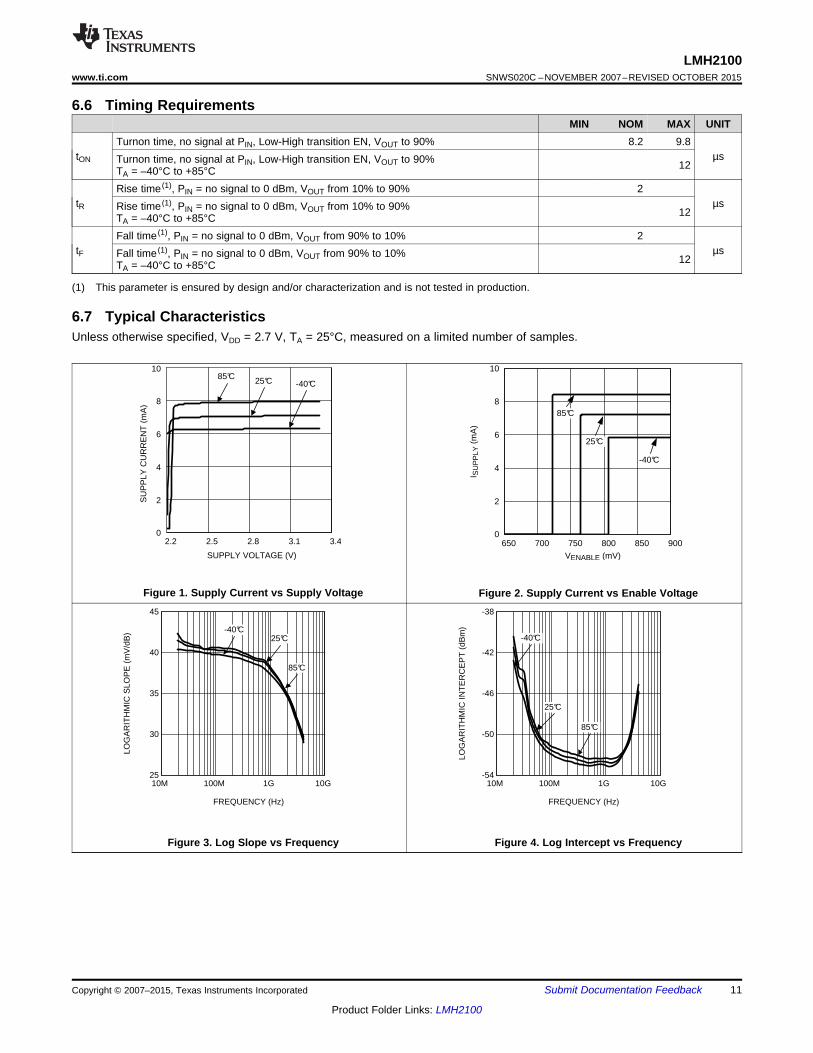
6.6 Timing RequirementsMIN NOM MAX UNIT
Turnon time, no signal at PIN, Low-High transition EN, VOUT to 90% 8.2 9.8tON µsTurnon time, no signal at PIN, Low-High transition EN, VOUT to 90% 12TA = –40°C to +85°C
Rise time (1), PIN = no signal to 0 dBm, VOUT from 10% to 90% 2tR µsRise time (1), PIN = no signal to 0 dBm, VOUT from 10% to 90% 12TA = –40°C to +85°C
Fall time (1), PIN = no signal to 0 dBm, VOUT from 90% to 10% 2tF µsFall time (1), PIN = no signal to 0 dBm, VOUT from 90% to 10% 12TA = –40°C to +85°C
(1) This parameter is ensured by design and/or characterization and is not tested in production.
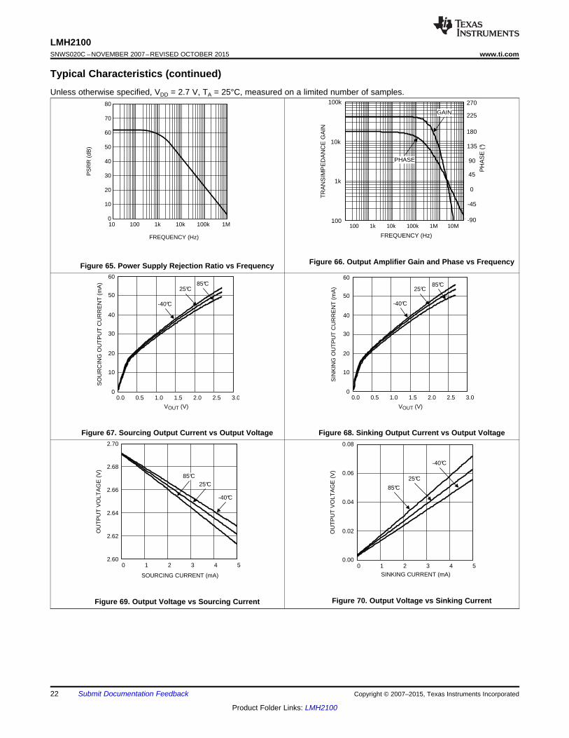
6.7 Typical CharacteristicsUnless otherwise specified, VDD = 2.7 V, TA = 25°C, measured on a limited number of samples.
Figure 1. Supply Current vs Supply Voltage Figure 2. Supply Current vs Enable Voltage
Figure 3. Log Slope vs Frequency Figure 4. Log Intercept vs Frequency
Copyright © 2007–2015, Texas Instruments Incorporated Submit Documentation Feedback 11
Product Folder Links: LMH2100
LOG
CO
NF
OR
MA
NC
E E
RR
OR
(dB
)
RF INPUT POWER (dBm)
VO
UT
(V)
2.01.81.61.41.21.00.80.60.40.20.0
2.52.01.51.00.50.0-0.5-1.0-1.5-2.0-2.5
-55 -45 -35 -25 -15 -5 5
-40°C
25°C
25°C
85°C
-40°C
85°C
2.0
1.8
1.6
1.4
1.0
1.2
0.8
0.6
0.4
0.0
0.2
2.5
2.0
1.5
1.0
0.0
0.5
-0.5
-1.0
-1.5
-2.5
-2.0LOG
CO
NF
OR
MA
NC
E E
RR
OR
(dB
)
RF INPUT POWER (dBm)
VO
UT
(V)
2.01.81.61.41.21.00.80.60.40.20.0
2.52.01.51.00.50.0-0.5-1.0-1.5-2.0-2.5
-55 -45 -35 -25 -15 -5 5
-40°C
25°C
25°C
85°C
-40°C
85°C
2.0
1.8
1.6
1.4
1.0
1.2
0.8
0.6
0.4
0.0
0.2
2.5
2.0
1.5
1.0
0.0
0.5
-0.5
-1.0
-1.5
-2.5
-2.0
LOG
CO
NF
OR
MA
NC
E E
RR
OR
(dB
)
RF INPUT POWER (dBm)
VO
UT
(V)
2.01.81.61.41.21.00.80.60.40.20.0
2.52.01.51.00.50.0-0.5-1.0-1.5-2.0-2.5
-55 -45 -35 -25 -15 -5 5
-40°C
25°C
25°C
85°C
-40°C
85°C
2.0
1.8
1.6
1.4
1.0
1.2
0.8
0.6
0.4
0.0
0.2
2.5
2.0
1.5
1.0
0.0
0.5
-0.5
-1.0
-1.5
-2.5
-2.0 LOG
CO
NF
OR
MA
NC
E E
RR
OR
(dB
)
RF INPUT POWER (dBm)
VO
UT
(V)
2.01.81.61.41.21.00.80.60.40.20.0
2.52.01.51.00.50.0-0.5-1.0-1.5-2.0-2.5
-55 -45 -35 -25 -15 -5 5
-40°C
25°C
25°C
85°C -40°C
85°C
2.0
1.8
1.6
1.4
1.0
1.2
0.8
0.6
0.4
0.0
0.2
2.5
2.0
1.5
1.0
0.0
0.5
-0.5
-1.0
-1.5
-2.5
-2.0
LOG
CO
NF
OR
MA
NC
E E
RR
OR
(dB
)
RF INPUT POWER (dBm)
VO
UT
(V)
2.01.81.61.41.21.00.80.60.40.20.0
2.52.01.51.00.50.0-0.5-1.0-1.5-2.0-2.5
-55 -45 -35 -25 -15 -5 5
-40°C
25°C
25°C
85°C
-40°C
85°C
2.0
1.8
1.6
1.4
1.0
1.2
0.8
0.6
0.4
0.0
0.2
2.5
2.0
1.5
1.0
0.0
0.5
-0.5
-1.0
-1.5
-2.5
-2.0 LOG
CO
NF
OR
MA
NC
E E
RR
OR
(dB
)
RF INPUT POWER (dBm)
VO
UT
(V)
2.01.81.61.41.21.00.80.60.40.20.0
2.52.01.51.00.50.0-0.5-1.0-1.5-2.0-2.5
-55 -45 -35 -25 -15 -5 5
-40°C
25°C
25°C
85°C
-40°C
85°C
2.0
1.8
1.6
1.4
1.0
1.2
0.8
0.6
0.4
0.0
0.2
2.5
2.0
1.5
1.0
0.0
0.5
-0.5
-1.0
-1.5
-2.5
-2.0
LMH2100SNWS020C –NOVEMBER 2007–REVISED OCTOBER 2015 www.ti.com
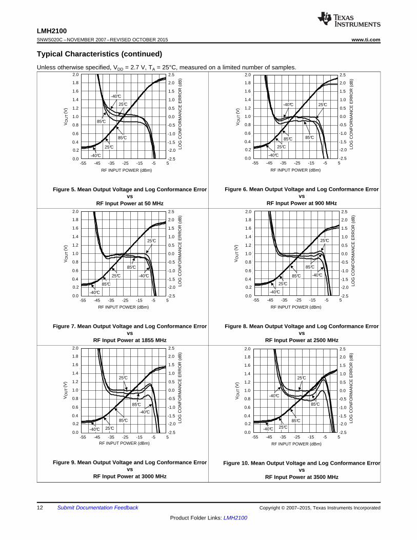
Typical Characteristics (continued)Unless otherwise specified, VDD = 2.7 V, TA = 25°C, measured on a limited number of samples.
Figure 6. Mean Output Voltage and Log Conformance ErrorFigure 5. Mean Output Voltage and Log Conformance Errorvsvs
RF Input Power at 900 MHzRF Input Power at 50 MHz
Figure 7. Mean Output Voltage and Log Conformance Error Figure 8. Mean Output Voltage and Log Conformance Errorvs vs
RF Input Power at 1855 MHz RF Input Power at 2500 MHz
Figure 9. Mean Output Voltage and Log Conformance Error Figure 10. Mean Output Voltage and Log Conformance Errorvs vs
RF Input Power at 3000 MHz RF Input Power at 3500 MHz
12 Submit Documentation Feedback Copyright © 2007–2015, Texas Instruments Incorporated
Product Folder Links: LMH2100
LOG
CO
NF
OR
MA
NC
E E
RR
OR
(dB
)
RF INPUT POWER (dBm)
VO
UT
(V)
2.01.81.61.41.21.00.80.60.40.20.0
2.52.01.51.00.50.0-0.5-1.0-1.5-2.0-2.5
-55 -45 -35 -25 -15 -5 5
-40°C
25°C
25°C
85°C
-40°C85°C
2.0
1.8
1.6
1.4
1.0
1.2
0.8
0.6
0.4
0.0
0.2
2.5
2.0
1.5
1.0
0.0
0.5
-0.5
-1.0
-1.5
-2.5
-2.0
LMH2100www.ti.com SNWS020C –NOVEMBER 2007–REVISED OCTOBER 2015
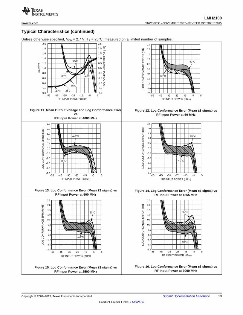
Typical Characteristics (continued)Unless otherwise specified, VDD = 2.7 V, TA = 25°C, measured on a limited number of samples.
Figure 11. Mean Output Voltage and Log Conformance Error Figure 12. Log Conformance Error (Mean ±3 sigma) vsvs RF Input Power at 50 MHz
RF Input Power at 4000 MHz
Figure 13. Log Conformance Error (Mean ±3 sigma) vs Figure 14. Log Conformance Error (Mean ±3 sigma) vsRF Input Power at 900 MHz RF Input Power at 1855 MHz
Figure 16. Log Conformance Error (Mean ±3 sigma) vsFigure 15. Log Conformance Error (Mean ±3 sigma) vsRF Input Power at 3000 MHzRF Input Power at 2500 MHz
Copyright © 2007–2015, Texas Instruments Incorporated Submit Documentation Feedback 13
Product Folder Links: LMH2100
RF INPUT POWER (dBm)
TE
MP
ER
AT
UR
E D
RIF
T (
dB)
1.5
1.0
0.5
0.0
-0.5
-1.0
-1.5
-55 -45 -35 -25 -15 -5 5
-40°C
85°C
1.5
1.0
0.5
0.0
-0.5
-1.5
-1.0
RF INPUT POWER (dBm)
TE
MP
ER
AT
UR
E D
RIF
T (
dB)
1.5
1.0
0.5
0.0
-0.5
-1.0
-1.5
-55 -45 -35 -25 -15 -5 5
-40°C
85°C
1.5
1.0
0.5
0.0
-0.5
-1.5
-1.0
RF INPUT POWER (dBm)
TE
MP
ER
AT
UR
E D
RIF
T (
dB) 1.5
1.0
0.5
0.0
-0.5
-1.0
-1.5
-55 -45 -35 -25 -15 -5 5
-40°C
85°C
1.5
1.0
0.5
0.0
-0.5
-1.5
-1.0
RF INPUT POWER (dBm)
TE
MP
ER
AT
UR
E D
RIF
T (
dB)
1.5
1.0
0.5
0.0
-0.5
-1.0
-1.5
-55 -45 -35 -25 -15 -5 5
-40°C
85°C
1.5
1.0
0.5
0.0
-0.5
-1.5
-1.0
LMH2100SNWS020C –NOVEMBER 2007–REVISED OCTOBER 2015 www.ti.com
Typical Characteristics (continued)Unless otherwise specified, VDD = 2.7 V, TA = 25°C, measured on a limited number of samples.
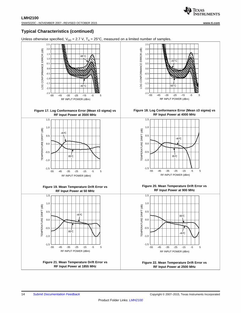
Figure 18. Log Conformance Error (Mean ±3 sigma) vsFigure 17. Log Conformance Error (Mean ±3 sigma) vsRF Input Power at 4000 MHzRF Input Power at 3500 MHz
Figure 20. Mean Temperature Drift Error vsFigure 19. Mean Temperature Drift Error vsRF Input Power at 900 MHzRF Input Power at 50 MHz
Figure 21. Mean Temperature Drift Error vs Figure 22. Mean Temperature Drift Error vsRF Input Power at 1855 MHz RF Input Power at 2500 MHz
14 Submit Documentation Feedback Copyright © 2007–2015, Texas Instruments Incorporated
Product Folder Links: LMH2100
RF INPUT POWER (dBm)
TE
MP
ER
AT
UR
E D
RIF
T (
dB) 1.5
1.0
0.5
0.0
-0.5
-1.0
-1.5
-55 -45 -35 -25 -15 -5 5
-40°C
85°C
1.5
1.0
0.5
0.0
-0.5
-1.5
-1.0
RF INPUT POWER (dBm)
TE
MP
ER
AT
UR
E D
RIF
T (
dB) 1.5
1.0
0.5
0.0
-0.5
-1.0
-1.5
-55 -45 -35 -25 -15 -5 5
-40°C
85°C
1.5
1.0
0.5
0.0
-0.5
-1.5
-1.0
RF INPUT POWER (dBm)
TE
MP
ER
AT
UR
E D
RIF
T (
dB) 1.5
1.0
0.5
0.0
-0.5
-1.0
-1.5
-55 -45 -35 -25 -15 -5 5
-40°C
85°C
1.5
1.0
0.5
0.0
-0.5
-1.5
-1.0
LMH2100www.ti.com SNWS020C –NOVEMBER 2007–REVISED OCTOBER 2015
Typical Characteristics (continued)Unless otherwise specified, VDD = 2.7 V, TA = 25°C, measured on a limited number of samples.
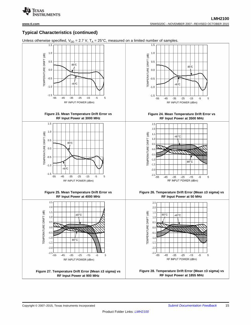
Figure 23. Mean Temperature Drift Error vs Figure 24. Mean Temperature Drift Error vsRF Input Power at 3000 MHz RF Input Power at 3500 MHz
Figure 25. Mean Temperature Drift Error vs Figure 26. Temperature Drift Error (Mean ±3 sigma) vsRF Input Power at 4000 MHz RF Input Power at 50 MHz
Figure 28. Temperature Drift Error (Mean ±3 sigma) vsFigure 27. Temperature Drift Error (Mean ±3 sigma) vsRF Input Power at 1855 MHzRF Input Power at 900 MHz
Copyright © 2007–2015, Texas Instruments Incorporated Submit Documentation Feedback 15
Product Folder Links: LMH2100
RF INPUT POWER (dBm)
ER
RO
R (
dB)
0.3
0.2
0.1
0.0
-0.1
-0.2
-0.3
-55 -45 -35 -25 -15 -5 5
-40°C
85°C
0.3
0.2
0.1
0.0
-0.1
-0.3
-0.2
RF INPUT POWER (dBm)
ER
RO
R (
dB)
0.3
0.2
0.1
0.0
-0.1
-0.2
-0.3
-55 -45 -35 -25 -15 -5 5
-40°C
85°C
0.3
0.2
0.1
0.0
-0.1
-0.3
-0.2
LMH2100SNWS020C –NOVEMBER 2007–REVISED OCTOBER 2015 www.ti.com
Typical Characteristics (continued)Unless otherwise specified, VDD = 2.7 V, TA = 25°C, measured on a limited number of samples.
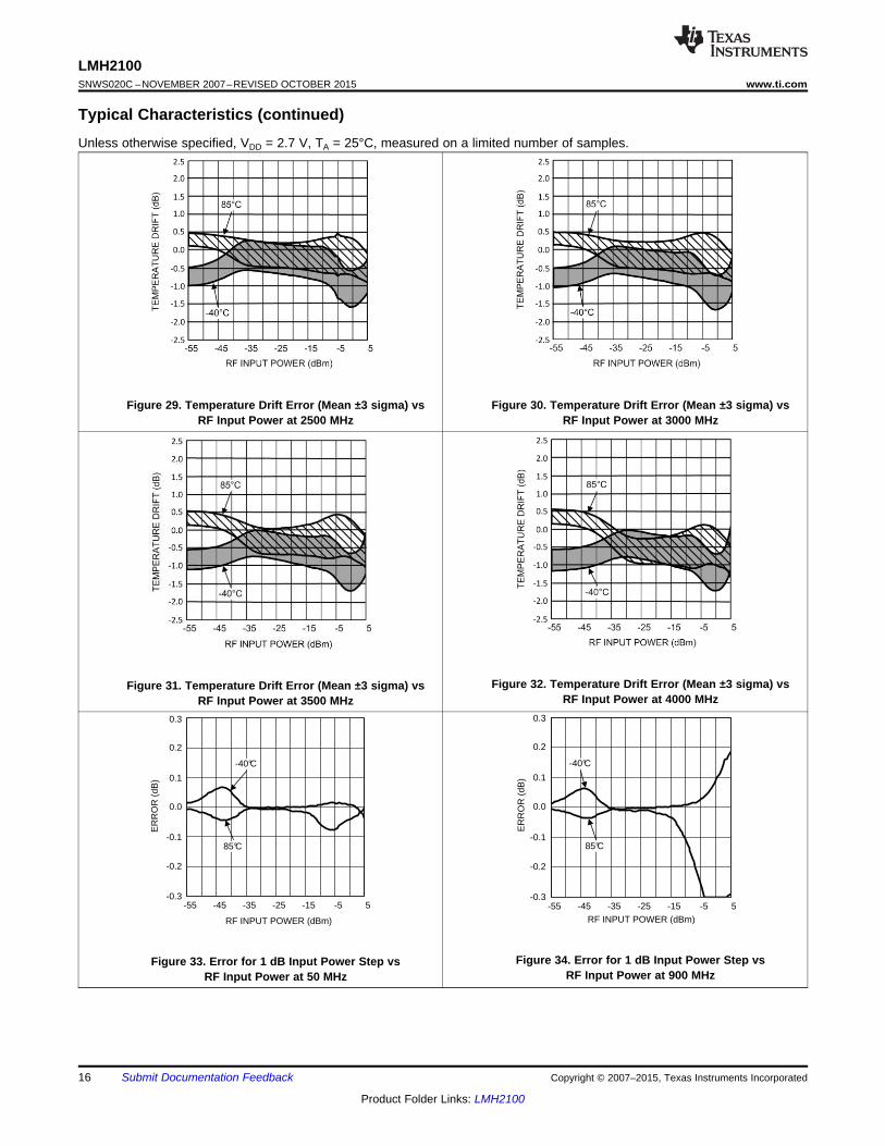
Figure 29. Temperature Drift Error (Mean ±3 sigma) vs Figure 30. Temperature Drift Error (Mean ±3 sigma) vsRF Input Power at 2500 MHz RF Input Power at 3000 MHz
Figure 32. Temperature Drift Error (Mean ±3 sigma) vsFigure 31. Temperature Drift Error (Mean ±3 sigma) vsRF Input Power at 4000 MHzRF Input Power at 3500 MHz
Figure 34. Error for 1 dB Input Power Step vsFigure 33. Error for 1 dB Input Power Step vsRF Input Power at 900 MHzRF Input Power at 50 MHz
16 Submit Documentation Feedback Copyright © 2007–2015, Texas Instruments Incorporated
Product Folder Links: LMH2100
RF INPUT POWER (dBm)
ER
RO
R (
dB)
0.3
0.2
0.1
0.0
-0.1
-0.2
-0.3
-55 -45 -35 -25 -15 -5 5
-40°C
85°C
0.3
0.2
0.1
0.0
-0.1
-0.3
-0.2
RF INPUT POWER (dBm)
ER
RO
R (
dB)
1.000.750.500.250.00
-0.25-0.50-0.75-1.00
-60 -50 -40 -30 -20 -10 0
-40°C
85°C
1.00
0.75
0.50
0.25
0.00
-0.25
-0.50
-1.00
-0.75
RF INPUT POWER (dBm)
ER
RO
R (
dB)
0.3
0.2
0.1
0.0
-0.1
-0.2
-0.3
-55 -45 -35 -25 -15 -5 5
-40°C
85°C
0.3
0.2
0.1
0.0
-0.1
-0.3
-0.2
RF INPUT POWER (dBm)
ER
RO
R (
dB)
0.3
0.2
0.1
0.0
-0.1
-0.2
-0.3
-55 -45 -35 -25 -15 -5 5
-40°C
85°C
0.3
0.2
0.1
0.0
-0.1
-0.3
-0.2
RF INPUT POWER (dBm)
ER
RO
R (
dB)
0.3
0.2
0.1
0.0
-0.1
-0.2
-0.3
-55 -45 -35 -25 -15 -5 5
-40°C
85°C
0.3
0.2
0.1
0.0
-0.1
-0.3
-0.2
RF INPUT POWER (dBm)
ER
RO
R (
dB)
0.3
0.2
0.1
0.0
-0.1
-0.2
-0.3
-55 -45 -35 -25 -15 -5 5
-40°C
85°C
0.3
0.2
0.1
0.0
-0.1
-0.3
-0.2
LMH2100www.ti.com SNWS020C –NOVEMBER 2007–REVISED OCTOBER 2015
Typical Characteristics (continued)Unless otherwise specified, VDD = 2.7 V, TA = 25°C, measured on a limited number of samples.
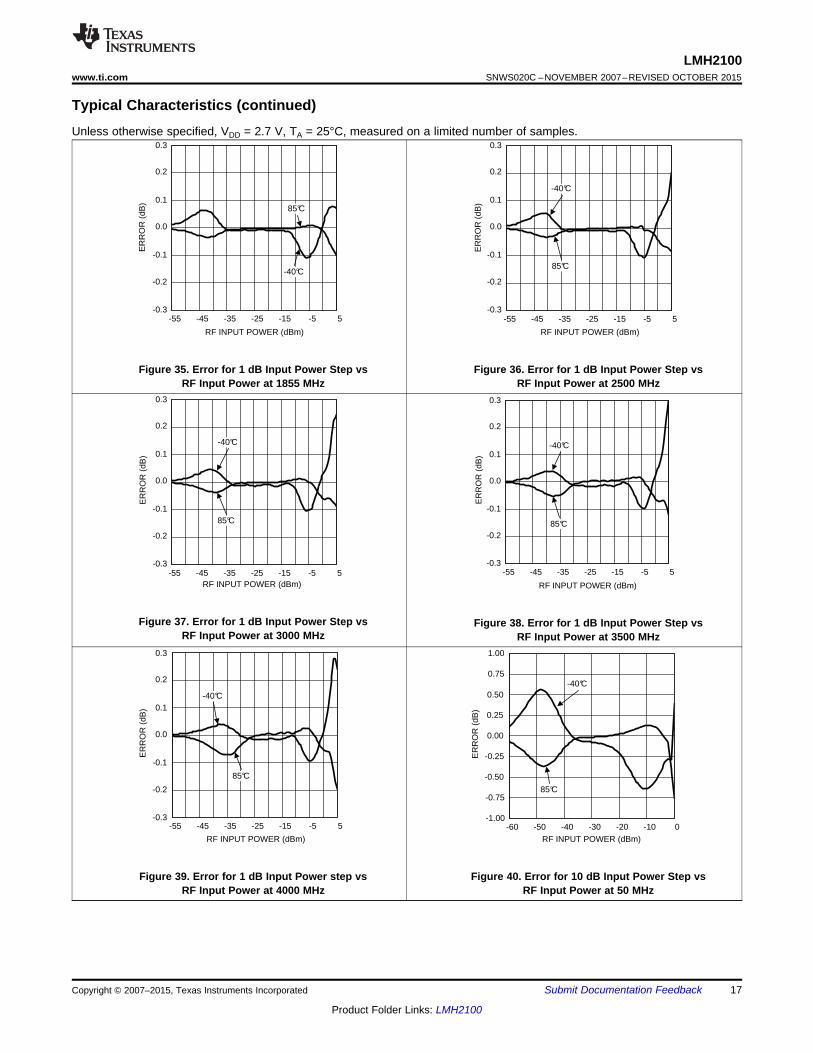
Figure 35. Error for 1 dB Input Power Step vs Figure 36. Error for 1 dB Input Power Step vsRF Input Power at 1855 MHz RF Input Power at 2500 MHz
Figure 37. Error for 1 dB Input Power Step vs Figure 38. Error for 1 dB Input Power Step vsRF Input Power at 3000 MHz RF Input Power at 3500 MHz
Figure 39. Error for 1 dB Input Power step vs Figure 40. Error for 10 dB Input Power Step vsRF Input Power at 4000 MHz RF Input Power at 50 MHz
Copyright © 2007–2015, Texas Instruments Incorporated Submit Documentation Feedback 17
Product Folder Links: LMH2100
RF INPUT POWER (dBm)
ER
RO
R (
dB)
1.000.750.500.250.00
-0.25-0.50-0.75-1.00
-60 -50 -40 -30 -20 -10 0
-40°C
85°C
1.00
0.75
0.50
0.25
0.00
-0.25
-0.50
-1.00
-0.75
RF INPUT POWER (dBm)
ER
RO
R (
dB)
1.000.750.500.250.00
-0.25-0.50-0.75-1.00
-60 -50 -40 -30 -20 -10 0
-40°C
85°C
1.00
0.75
0.50
0.25
0.00
-0.25
-0.50
-1.00
-0.75
RF INPUT POWER (dBm)
ER
RO
R (
dB)
1.000.750.500.250.00
-0.25-0.50-0.75-1.00
-60 -50 -40 -30 -20 -10 0
-40°C
85°C
1.00
0.75
0.50
0.25
0.00
-0.25
-0.50
-1.00
-0.75
RF INPUT POWER (dBm)
ER
RO
R (
dB)
1.000.750.500.250.00
-0.25-0.50-0.75-1.00
-60 -50 -40 -30 -20 -10 0
-40°C
85°C
1.00
0.75
0.50
0.25
0.00
-0.25
-0.50
-1.00
-0.75
RF INPUT POWER (dBm)
ER
RO
R (
dB)
1.000.750.500.250.00
-0.25-0.50-0.75-1.00
-60 -50 -40 -30 -20 -10 0
-40°C
85°C
1.00
0.75
0.50
0.25
0.00
-0.25
-0.50
-1.00
-0.75
RF INPUT POWER (dBm)
ER
RO
R (
dB)
1.000.750.500.250.00
-0.25-0.50-0.75-1.00
-60 -50 -40 -30 -20 -10 0
-40°C
85°C
1.00
0.75
0.50
0.25
0.00
-0.25
-0.50
-1.00
-0.75
LMH2100SNWS020C –NOVEMBER 2007–REVISED OCTOBER 2015 www.ti.com
Typical Characteristics (continued)Unless otherwise specified, VDD = 2.7 V, TA = 25°C, measured on a limited number of samples.
Figure 42. Error for 10 dB Input Power Step vsFigure 41. Error for 10 dB Input Power Step vsRF Input Power at 1855 MHzRF Input Power at 900 MHz
Figure 44. Error for 10 dB Input Power Step vsFigure 43. Error for 10 dB Input Power Step vsRF Input Power at 3000 MHzRF Input Power at 2500 MHz
Figure 46. Error for 10 dB Input Power step vsFigure 45. Error for 10 dB Input Power Step vsRF Input Power at 4000 MHzRF Input Power at 3500 MHz
18 Submit Documentation Feedback Copyright © 2007–2015, Texas Instruments Incorporated
Product Folder Links: LMH2100
RF INPUT POWER (dBm)
SE
NS
ITIV
ITY
(m
dB/°C
)
201510
50
-5-10-15-20
-55 -45 -35 -25 -15 -5 5
-40°C
85°C
20
15
10
5
0
-5
-10
-20
-15
RF INPUT POWER (dBm)
SE
NS
ITIV
ITY
(m
dB/°C
)
201510
50
-5-10-15-20
-55 -45 -35 -25 -15 -5 5
-40°C
85°C
20
15
10
5
0
-5
-10
-20
-15
RF INPUT POWER (dBm)
SE
NS
ITIV
ITY
(m
dB/°C
)
201510
50
-5-10-15-20
-55 -45 -35 -25 -15 -5 5
-40°C
85°C
20
15
10
5
0
-5
-10
-20
-15
RF INPUT POWER (dBm)
SE
NS
ITIV
ITY
(m
dB/°C
)
201510
50
-5-10-15-20
-55 -45 -35 -25 -15 -5 5
-40°C
85°C
20
15
10
5
0
-5
-10
-20
-15
RF INPUT POWER (dBm)
SE
NS
ITIV
ITY
(m
dB/°C
)
201510
50
-5-10-15-20
-55 -45 -35 -25 -15 -5 5
-40°C
85°C
20
15
10
5
0
-5
-10
-20
-15
RF INPUT POWER (dBm)
SE
NS
ITIV
ITY
(m
dB/°C
)
201510
50
-5-10-15-20
-55 -45 -35 -25 -15 -5 5
-40°C
85°C
20
15
10
5
0
-5
-10
-20
-15
LMH2100www.ti.com SNWS020C –NOVEMBER 2007–REVISED OCTOBER 2015
Typical Characteristics (continued)Unless otherwise specified, VDD = 2.7 V, TA = 25°C, measured on a limited number of samples.
Figure 47. Mean Temperature Sensitivity vs Figure 48. Mean Temperature Sensitivity vsRF Input Power at 50 MHz RF Input Power at 900 MHz
Figure 49. Mean Temperature Sensitivity vs Figure 50. Mean Temperature Sensitivity vsRF Input Power at 1855 MHz RF Input Power at 2500 MHz
Figure 51. Mean Temperature Sensitivity vs Figure 52. Mean Temperature Sensitivity vsRF Input Power at 3000 MHz RF Input Power at 3500 MHz
Copyright © 2007–2015, Texas Instruments Incorporated Submit Documentation Feedback 19
Product Folder Links: LMH2100
RF INPUT POWER (dBm)
SE
NS
ITIV
ITY
(md
B/°
C)
20
15
10
5
0
-5
-10
-15
-20-55 -45 -35 -25 -15 -5 5
85°C
-40°C
RF INPUT POWER (dBm)
SE
NS
ITIV
ITY
(md
B/°
C)
20
15
-15
-20-55 -45 -35 -25 -15 -5 5
-40°C
10
5
0
-5
-10
85°C
RF INPUT POWER (dBm)
SE
NS
ITIV
ITY
(md
B/°
C)
20
15
10
5
0
-5
-10
-15
-20-55 -45 -35 -25 -15 -5 5
85°C
-40°C
RF INPUT POWER (dBm)
SE
NS
ITIV
ITY
(mdB
/°C
)
20
15
10
5
0
-5
-10
-15
-20-55 -45 -35 -25 -15 -5 5
85°C
-40°C
RF INPUT POWER (dBm)
SE
NS
ITIV
ITY
(md
B/°
C)
20
15
10
5
0
-5
-10
-15
-20-55 -45 -35 -25 -15 -5 5
85°C
-40°C
RF INPUT POWER (dBm)
SE
NS
ITIV
ITY
(m
dB/°C
)
201510
50
-5-10-15-20
-55 -45 -35 -25 -15 -5 5
-40°C
85°C
20
15
10
5
0
-5
-10
-20
-15
LMH2100SNWS020C –NOVEMBER 2007–REVISED OCTOBER 2015 www.ti.com
Typical Characteristics (continued)Unless otherwise specified, VDD = 2.7 V, TA = 25°C, measured on a limited number of samples.
Figure 53. Mean Temperature Sensitivity vsFigure 54. Temperature Sensitivity (Mean ±3 sigma) vsRF Input power at 4000 MHz
RF Input Power at 50 MHz
Figure 55. Temperature Sensitivity (Mean ±3 sigma) vs Figure 56. Temperature Sensitivity (Mean ±3 sigma) vsRF Input Power at 900 MHz RF Input Power at 1855 MHz
Figure 57. Temperature Sensitivity (Mean ±3 sigma) vs Figure 58. Temperature Sensitivity (Mean ±3 sigma) vsRF Input Power at 2500 MHz RF Input Power at 3000 MHz
20 Submit Documentation Feedback Copyright © 2007–2015, Texas Instruments Incorporated
Product Folder Links: LMH2100
FREQUENCY (Hz)
RF
INP
UT
IMP
ED
AN
CE
(Ö
)
100
75
50
25
0
-25
-50
-75
-10010M 100M 1G 10G
R
X
FREQUENCY (Hz)
VO
LTA
GE
NO
ISE
(µ
V/
Hz)
10
9
8
7
6
5
4
3
2
1
010 100 1k 10k 100k 1M
LOG
CO
NF
OR
MA
NC
E E
RR
OR
(dB
)
RF INPUT POWER (dBm)
VO
UT
(V)
2.01.81.61.41.21.00.80.60.40.20.0
2.52.01.51.00.50.0-0.5-1.0-1.5-2.0-2.5
-55 -45 -35 -25 -15 -5 5
CW
IS-95
WCDMA 64 CH
CW
WCDMA 64 ch
IS-95
2.0
1.8
1.6
1.4
1.0
1.2
0.8
0.6
0.4
0.0
0.2
2.5
2.0
1.5
1.0
0.0
0.5
-0.5
-1.0
-1.5
-2.5
-2.0LOG
CO
NF
OR
MA
NC
E E
RR
OR
(dB
)
RF INPUT POWER (dBm)
VO
UT
(V)
2.01.81.61.41.21.00.80.60.40.20.0
2.52.01.51.00.50.0-0.5-1.0-1.5-2.0-2.5
-55 -45 -35 -25 -15 -5 5
CW
IS-95
IS-95
WCDMA 64 CH
CW
WCDMA 64 ch
2.0
1.8
1.6
1.4
1.0
1.2
0.8
0.6
0.4
0.0
0.2
2.5
2.0
1.5
1.0
0.0
0.5
-0.5
-1.0
-1.5
-2.5
-2.0
RF INPUT POWER (dBm)
SE
NS
ITIV
ITY
(md
B/°
C)
20
15
10
5
0
-5
-10
-15
-20-55 -45 -35 -25 -15 -5 5
85°C
-40°C
RF INPUT POWER (dBm)
SE
NS
ITIV
ITY
(md
B/°
C)
20
15
10
5
0
-5
-10
-15
-20-55 -45 -35 -25 -15 -5 5
85°C
-40°C
LMH2100www.ti.com SNWS020C –NOVEMBER 2007–REVISED OCTOBER 2015
Typical Characteristics (continued)Unless otherwise specified, VDD = 2.7 V, TA = 25°C, measured on a limited number of samples.
Figure 59. Temperature Sensitivity (Mean ±3 sigma) vs Figure 60. Temperature Sensitivity (mean ±3 sigma) vs.RF Input Power at 3500 MHz RF Input Power at 4000 MHz
Figure 61. Output Voltage and Log Conformance Error vs Figure 62. Output Voltage and Log Conformance Error vsRF Input Power for Various Modulation Types at 900 MHz RF Input Power for Various Modulation Types at 1855 MHz
Figure 63. RF Input Impedance vs Figure 64. Output Noise Spectrum vs FrequencyFrequency (Resistance and Reactance)
Copyright © 2007–2015, Texas Instruments Incorporated Submit Documentation Feedback 21
Product Folder Links: LMH2100
SOURCING CURRENT (mA)
OU
TP
UT
VO
LTA
GE
(V
)
2.70
2.68
2.66
2.64
2.62
2.60
0 1 2 3 4 5
25°C85°C
-40°C
2.70
2.68
2.66
2.64
2.62
2.60
SINKING CURRENT (mA)
OU
TP
UT
VO
LTA
GE
(V
)
0.08
0.06
0.04
0.02
0.00
0 1 2 3 4 5
85°C
25°C
-40°C
0.08
0.06
0.04
0.02
0.00
VOUT (V)
SO
UR
CIN
G O
UT
PU
T C
UR
RE
NT
(m
A)
60
50
40
30
20
10
0
0.0 0.5 1.0 1.5 2.0 2.5 3.0
25°C85°C
-40°C
60
50
40
30
20
0
10
VOUT (V)
SIN
KIN
G O
UT
PU
T C
UR
RE
NT
(m
A)
60
50
40
30
20
10
0
0.0 0.5 1.0 1.5 2.0 2.5 3.0
25°C85°C
-40°C
60
50
40
30
20
0
10
FREQUENCY (Hz)
PS
RR
(dB
)
80
70
60
50
40
30
20
10
010 100 1k 10k 100k 1M
PH
AS
E (
°)
FREQUENCY (Hz)
TR
AN
SIM
PE
DA
NC
E G
AIN
100k
10k
1k
100
27022518013590450-45-90
GAIN
PHASE
100 1k 10k 100k 1M 10M
100k
10k
100
1k
270
225
180
135
45
90
0
-45
-90
LMH2100SNWS020C –NOVEMBER 2007–REVISED OCTOBER 2015 www.ti.com
Typical Characteristics (continued)Unless otherwise specified, VDD = 2.7 V, TA = 25°C, measured on a limited number of samples.
Figure 66. Output Amplifier Gain and Phase vs FrequencyFigure 65. Power Supply Rejection Ratio vs Frequency
Figure 67. Sourcing Output Current vs Output Voltage Figure 68. Sinking Output Current vs Output Voltage
Figure 70. Output Voltage vs Sinking CurrentFigure 69. Output Voltage vs Sourcing Current
22 Submit Documentation Feedback Copyright © 2007–2015, Texas Instruments Incorporated
Product Folder Links: LMH2100
OUT
V-V 10 dBRFIN
10 dB
EN
VDD
GND
I / I
10 dB 10 dB
-
+
REF
VREF+-
en
en
en
RIN
RTRANS
A1
C2
B1
C1
A2
B2
LMH2100www.ti.com SNWS020C –NOVEMBER 2007–REVISED OCTOBER 2015
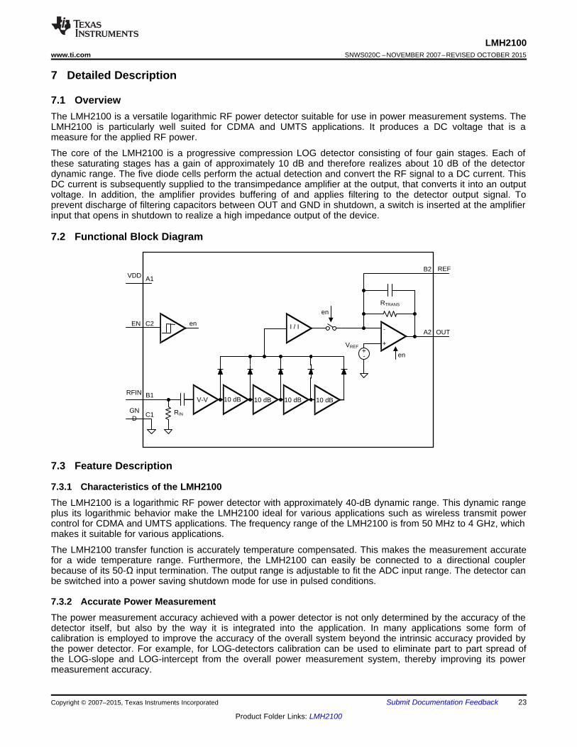
7 Detailed Description
7.1 OverviewThe LMH2100 is a versatile logarithmic RF power detector suitable for use in power measurement systems. TheLMH2100 is particularly well suited for CDMA and UMTS applications. It produces a DC voltage that is ameasure for the applied RF power.
The core of the LMH2100 is a progressive compression LOG detector consisting of four gain stages. Each ofthese saturating stages has a gain of approximately 10 dB and therefore realizes about 10 dB of the detectordynamic range. The five diode cells perform the actual detection and convert the RF signal to a DC current. ThisDC current is subsequently supplied to the transimpedance amplifier at the output, that converts it into an outputvoltage. In addition, the amplifier provides buffering of and applies filtering to the detector output signal. Toprevent discharge of filtering capacitors between OUT and GND in shutdown, a switch is inserted at the amplifierinput that opens in shutdown to realize a high impedance output of the device.
7.2 Functional Block Diagram
7.3 Feature Description
7.3.1 Characteristics of the LMH2100The LMH2100 is a logarithmic RF power detector with approximately 40-dB dynamic range. This dynamic rangeplus its logarithmic behavior make the LMH2100 ideal for various applications such as wireless transmit powercontrol for CDMA and UMTS applications. The frequency range of the LMH2100 is from 50 MHz to 4 GHz, whichmakes it suitable for various applications.
The LMH2100 transfer function is accurately temperature compensated. This makes the measurement accuratefor a wide temperature range. Furthermore, the LMH2100 can easily be connected to a directional couplerbecause of its 50-Ω input termination. The output range is adjustable to fit the ADC input range. The detector canbe switched into a power saving shutdown mode for use in pulsed conditions.
7.3.2 Accurate Power MeasurementThe power measurement accuracy achieved with a power detector is not only determined by the accuracy of thedetector itself, but also by the way it is integrated into the application. In many applications some form ofcalibration is employed to improve the accuracy of the overall system beyond the intrinsic accuracy provided bythe power detector. For example, for LOG-detectors calibration can be used to eliminate part to part spread ofthe LOG-slope and LOG-intercept from the overall power measurement system, thereby improving its powermeasurement accuracy.
Copyright © 2007–2015, Texas Instruments Incorporated Submit Documentation Feedback 23
Product Folder Links: LMH2100
ELCE = PEST - PIN = - (PIN - PINTERCEPT ) VOUT
KSLOPE
VOUT - VOUT,MOD
KSLOPE =
PEST = FEST(VOUT) = + PINTERCEPT VOUT
KSLOPE
VOUT,MOD = FDET,MOD(PIN) = KSLOPE(PIN ± PINTERCEPT)
LMH2100SNWS020C –NOVEMBER 2007–REVISED OCTOBER 2015 www.ti.com
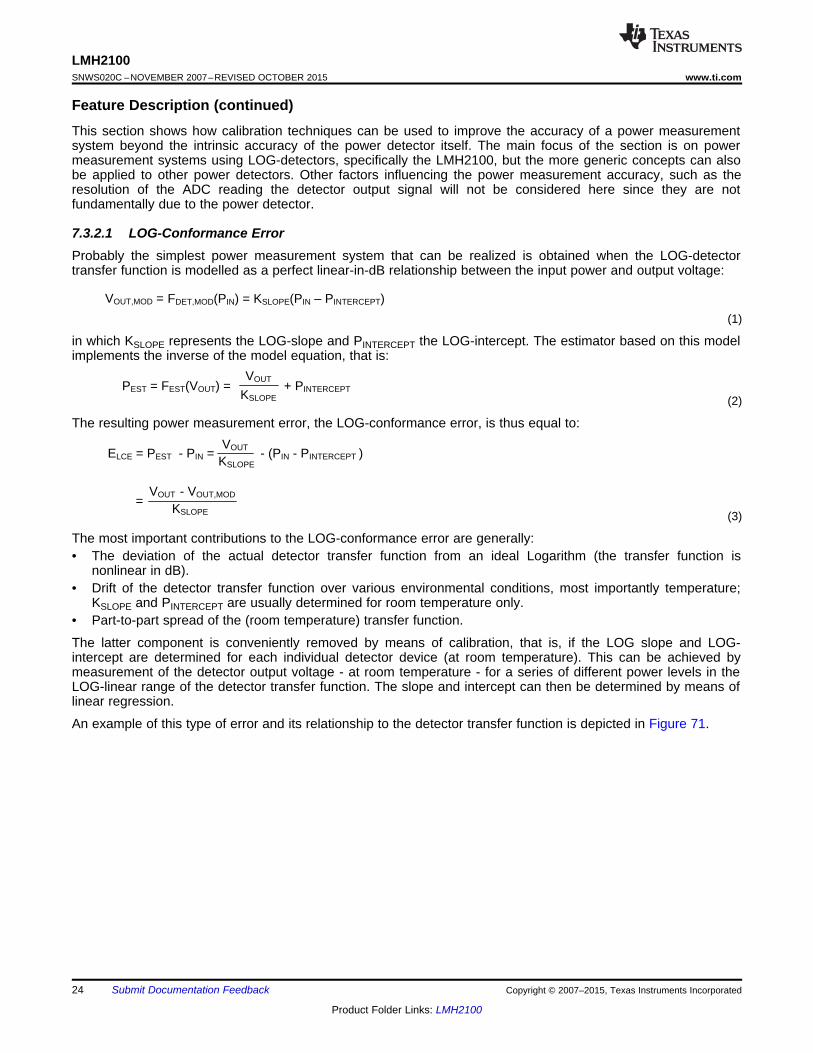
Feature Description (continued)This section shows how calibration techniques can be used to improve the accuracy of a power measurementsystem beyond the intrinsic accuracy of the power detector itself. The main focus of the section is on powermeasurement systems using LOG-detectors, specifically the LMH2100, but the more generic concepts can alsobe applied to other power detectors. Other factors influencing the power measurement accuracy, such as theresolution of the ADC reading the detector output signal will not be considered here since they are notfundamentally due to the power detector.
7.3.2.1 LOG-Conformance ErrorProbably the simplest power measurement system that can be realized is obtained when the LOG-detectortransfer function is modelled as a perfect linear-in-dB relationship between the input power and output voltage:
(1)
in which KSLOPE represents the LOG-slope and PINTERCEPT the LOG-intercept. The estimator based on this modelimplements the inverse of the model equation, that is:
(2)
The resulting power measurement error, the LOG-conformance error, is thus equal to:
(3)
The most important contributions to the LOG-conformance error are generally:• The deviation of the actual detector transfer function from an ideal Logarithm (the transfer function is
nonlinear in dB).• Drift of the detector transfer function over various environmental conditions, most importantly temperature;
KSLOPE and PINTERCEPT are usually determined for room temperature only.• Part-to-part spread of the (room temperature) transfer function.
The latter component is conveniently removed by means of calibration, that is, if the LOG slope and LOG-intercept are determined for each individual detector device (at room temperature). This can be achieved bymeasurement of the detector output voltage - at room temperature - for a series of different power levels in theLOG-linear range of the detector transfer function. The slope and intercept can then be determined by means oflinear regression.
An example of this type of error and its relationship to the detector transfer function is depicted in Figure 71.
24 Submit Documentation Feedback Copyright © 2007–2015, Texas Instruments Incorporated
Product Folder Links: LMH2100
EDRIFT (T,T0) = PEST - PIN = FDET[VOUT(T),T0] - PIN
= FDET[VOUT(T),T0] - FDET[VOUT(T),T)]-1
-1
-1
PEST = FDET[VOUT(T),T0]-1
LOG
CO
NF
OR
MA
NC
E E
RR
OR
(dB
)
RF INPUT POWER (dBm)
VO
UT
(V)
2.01.81.61.41.21.00.80.60.40.20.0
2.52.01.51.00.50.0-0.5-1.0-1.5-2.0-2.5
-55 -45 -35 -25 -15 -5 5
-40°C
25°C
25°C
85°C
-40°C
85°C
2.0
1.8
1.6
1.4
1.0
1.2
0.8
0.6
0.4
0.0
0.2
2.5
2.0
1.5
1.0
0.0
0.5
-0.5
-1.0
-1.5
-2.5
-2.0
LMH2100www.ti.com SNWS020C –NOVEMBER 2007–REVISED OCTOBER 2015
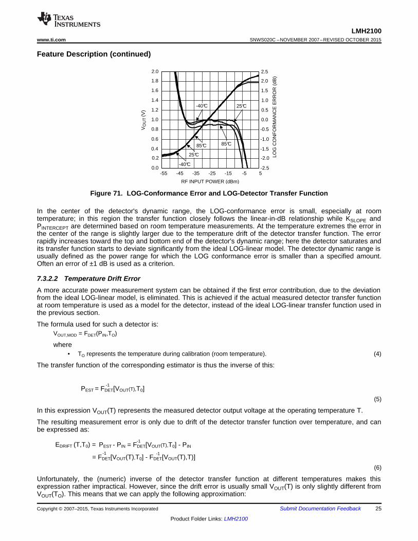
Feature Description (continued)
Figure 71. LOG-Conformance Error and LOG-Detector Transfer Function
In the center of the detector's dynamic range, the LOG-conformance error is small, especially at roomtemperature; in this region the transfer function closely follows the linear-in-dB relationship while KSLOPE andPINTERCEPT are determined based on room temperature measurements. At the temperature extremes the error inthe center of the range is slightly larger due to the temperature drift of the detector transfer function. The errorrapidly increases toward the top and bottom end of the detector's dynamic range; here the detector saturates andits transfer function starts to deviate significantly from the ideal LOG-linear model. The detector dynamic range isusually defined as the power range for which the LOG conformance error is smaller than a specified amount.Often an error of ±1 dB is used as a criterion.
7.3.2.2 Temperature Drift ErrorA more accurate power measurement system can be obtained if the first error contribution, due to the deviationfrom the ideal LOG-linear model, is eliminated. This is achieved if the actual measured detector transfer functionat room temperature is used as a model for the detector, instead of the ideal LOG-linear transfer function used inthe previous section.
The formula used for such a detector is:VOUT,MOD = FDET(PIN,TO)
where• TO represents the temperature during calibration (room temperature). (4)
The transfer function of the corresponding estimator is thus the inverse of this:
(5)
In this expression VOUT(T) represents the measured detector output voltage at the operating temperature T.
The resulting measurement error is only due to drift of the detector transfer function over temperature, and canbe expressed as:
(6)
Unfortunately, the (numeric) inverse of the detector transfer function at different temperatures makes thisexpression rather impractical. However, since the drift error is usually small VOUT(T) is only slightly different fromVOUT(TO). This means that we can apply the following approximation:
Copyright © 2007–2015, Texas Instruments Incorporated Submit Documentation Feedback 25
Product Folder Links: LMH2100
RF INPUT POWER (dBm)
TE
MP
ER
AT
UR
E D
RIF
T (
dB)
1.5
1.0
0.5
0.0
-0.5
-1.0
-1.5
-55 -45 -35 -25 -15 -5 5
-40°C
85°C
1.5
1.0
0.5
0.0
-0.5
-1.5
-1.0
EDRIFT (T,T0) | (T ± T0) FDET[VOUT(T),T0]-1w
w7
= (T ± T0) FDET[VOUT(T),T0]-1wVOUT(T)w
w7 wVOUT
| VOUT(T) ± VOUT(T0)
KSLOPE
EDRIFT(T,T0) | EDRIFT(T0,T0)
-1 -1
w7+ (T - T0) FDET[VOUT(T),T0] - FDET[VOUT(T),T]
w
LMH2100SNWS020C –NOVEMBER 2007–REVISED OCTOBER 2015 www.ti.com
Feature Description (continued)
(7)
This expression is easily simplified by taking the following considerations into account:• The drift error at the calibration temperature E(TO,TO) equals zero (by definition).• The estimator transfer FDET(VOUT,TO) is not a function of temperature; the estimator output changes over
temperature only due to the temperature dependence of VOUT.• The actual detector input power PIN is not temperature dependent (in the context of this expression).• The derivative of the estimator transfer function to VOUT equals approximately 1/KSLOPE in the LOG-linear
region of the detector transfer function (the region of interest).
Using this, we arrive at:
(8)
This expression is very similar to the expression of the LOG-conformance error determined previously. The onlydifference is that instead of the output of the ideal LOG-linear model, the actual detector output voltage at thecalibration temperature is now subtracted from the detector output voltage at the operating temperature.
Figure 72 depicts an example of the drift error.
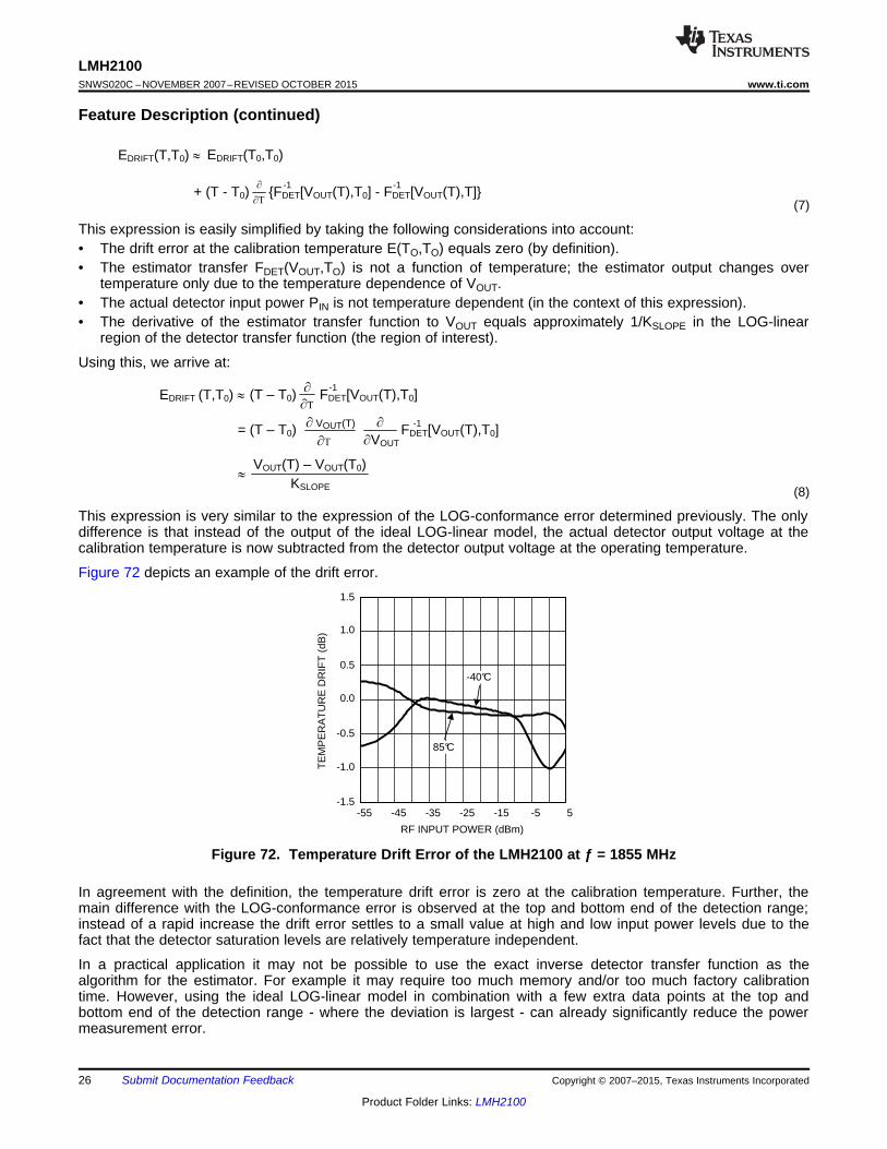
Figure 72. Temperature Drift Error of the LMH2100 at ƒ = 1855 MHz
In agreement with the definition, the temperature drift error is zero at the calibration temperature. Further, themain difference with the LOG-conformance error is observed at the top and bottom end of the detection range;instead of a rapid increase the drift error settles to a small value at high and low input power levels due to thefact that the detector saturation levels are relatively temperature independent.
In a practical application it may not be possible to use the exact inverse detector transfer function as thealgorithm for the estimator. For example it may require too much memory and/or too much factory calibrationtime. However, using the ideal LOG-linear model in combination with a few extra data points at the top andbottom end of the detection range - where the deviation is largest - can already significantly reduce the powermeasurement error.
26 Submit Documentation Feedback Copyright © 2007–2015, Texas Instruments Incorporated
Product Folder Links: LMH2100
T
ERROR
T
ERROR
AFTER
TEMPERATURE
CORRECTION
-3s
-3s
+3s
+3s
MEAN
MEAN
+ (T-T0)2S2[VOUT(T)] + O(T3)
| FDET[VOUT(T),T0]1 + (T-T0)S1[VOUT(T)]
-1
-1
PEST = FDET[VOUT(T),T0]1 + (T-T0)S1[VOUT(T)] +
VOUT,MOD = FDET(PIN,T0)[1 + (T-T0)TC1(PIN)
+ (T-T0)2TC2(PIN) + O(T3)]
LMH2100www.ti.com SNWS020C –NOVEMBER 2007–REVISED OCTOBER 2015
Feature Description (continued)7.3.2.2.1 Temperature Compensation
A further reduction of the power measurement error is possible if the operating temperature is measured in theapplication. For this purpose, the detector model used by the estimator should be extended to cover thetemperature dependency of the detector.
Since the detector transfer function is generally a smooth function of temperature (the output voltage changesgradually over temperature), the temperature is in most cases adequately modeled by a first-order or second-order polynomial (see Equation 9).
(9)
The required temperature dependence of the estimator, to compensate for the detector temperature dependencecan be approximated similarly:
(10)
The last approximation results from the fact that a first-order temperature compensation is usually sufficientlyaccurate. The remainder of this section will therefore concentrate on first-order compensation. For second andhigher-order compensation a similar approach can be followed.
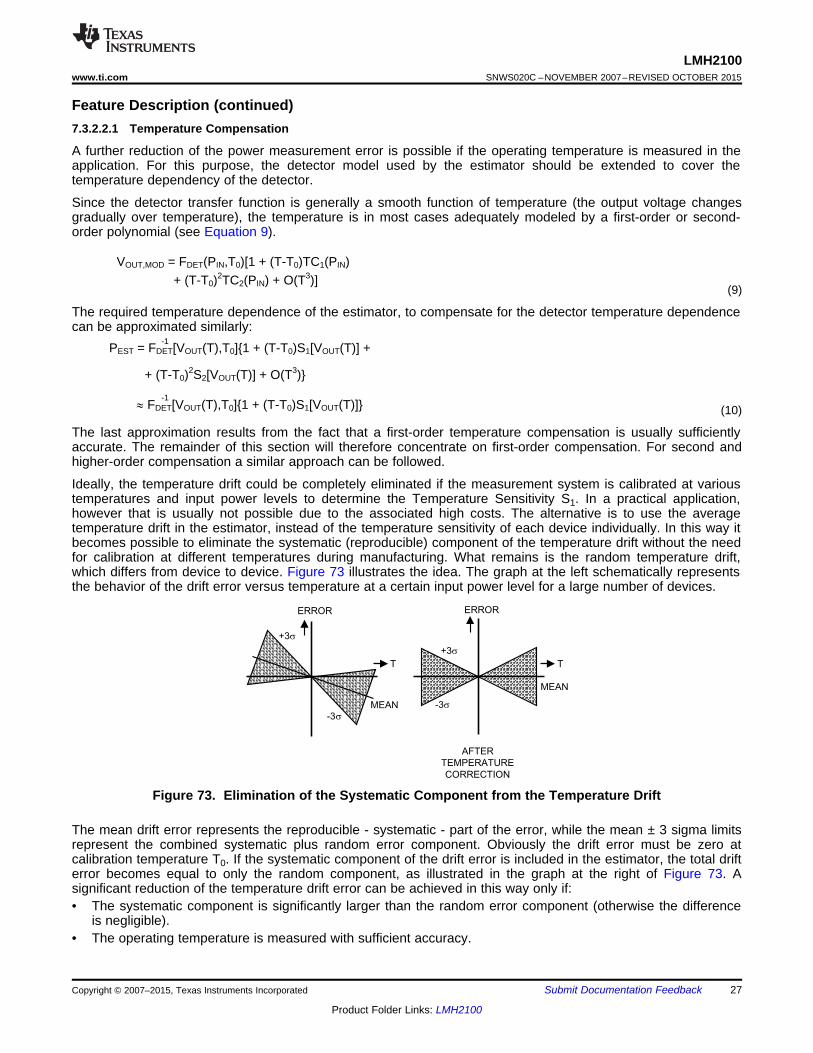
Ideally, the temperature drift could be completely eliminated if the measurement system is calibrated at varioustemperatures and input power levels to determine the Temperature Sensitivity S1. In a practical application,however that is usually not possible due to the associated high costs. The alternative is to use the averagetemperature drift in the estimator, instead of the temperature sensitivity of each device individually. In this way itbecomes possible to eliminate the systematic (reproducible) component of the temperature drift without the needfor calibration at different temperatures during manufacturing. What remains is the random temperature drift,which differs from device to device. Figure 73 illustrates the idea. The graph at the left schematically representsthe behavior of the drift error versus temperature at a certain input power level for a large number of devices.
Figure 73. Elimination of the Systematic Component from the Temperature Drift
The mean drift error represents the reproducible - systematic - part of the error, while the mean ± 3 sigma limitsrepresent the combined systematic plus random error component. Obviously the drift error must be zero atcalibration temperature T0. If the systematic component of the drift error is included in the estimator, the total drifterror becomes equal to only the random component, as illustrated in the graph at the right of Figure 73. Asignificant reduction of the temperature drift error can be achieved in this way only if:• The systematic component is significantly larger than the random error component (otherwise the difference
is negligible).• The operating temperature is measured with sufficient accuracy.
Copyright © 2007–2015, Texas Instruments Incorporated Submit Documentation Feedback 27
Product Folder Links: LMH2100
LMH2100SNWS020C –NOVEMBER 2007–REVISED OCTOBER 2015 www.ti.com
Feature Description (continued)It is essential for the effectiveness of the temperature compensation to assign the appropriate value to thetemperature sensitivity S1. Two different approaches can be followed to determine this parameter:• Determination of a single value to be used over the entire operating temperature range.• Division of the operating temperature range in segments and use of separate values for each of the
segments.
Also for the first method, the accuracy of the extracted temperature sensitivity increases when the number ofmeasurement temperatures increases. Linear regression to temperature can then be used to determine the twoparameters of the linear model for the temperature drift error: the first order temperature sensitivity S1 and thebest-fit (room temperature) value for the power estimate at T0: FDET[VOUT(T),T0]. Note that to achieve an overall -over all temperatures - minimum error, the room temperature drift error in the model can be non-zero at thecalibration temperature (which is not in agreement with the strict definition).
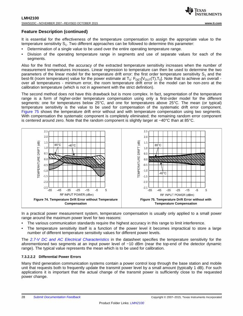
The second method does not have this drawback but is more complex. In fact, segmentation of the temperaturerange is a form of higher-order temperature compensation using only a first-order model for the differentsegments: one for temperatures below 25°C, and one for temperatures above 25°C. The mean (or typical)temperature sensitivity is the value to be used for compensation of the systematic drift error component.Figure 75 shows the temperature drift error without and with temperature compensation using two segments.With compensation the systematic component is completely eliminated; the remaining random error componentis centered around zero. Note that the random component is slightly larger at −40°C than at 85°C.
Figure 74. Temperature Drift Error without Temperature Figure 75. Temperature Drift Error without withCompensation Temperature Compensation
In a practical power measurement system, temperature compensation is usually only applied to a small powerrange around the maximum power level for two reasons:• The various communication standards require the highest accuracy in this range to limit interference.• The temperature sensitivity itself is a function of the power level it becomes impractical to store a large
number of different temperature sensitivity values for different power levels.
The 2.7-V DC and AC Electrical Characteristics in the datasheet specifies the temperature sensitivity for theaforementioned two segments at an input power level of −10 dBm (near the top-end of the detector dynamicrange). The typical value represents the mean which is to be used for calibration.
7.3.2.2.2 Differential Power Errors
Many third generation communication systems contain a power control loop through the base station and mobileunit that requests both to frequently update the transmit power level by a small amount (typically 1 dB). For suchapplications it is important that the actual change of the transmit power is sufficiently close to the requestedpower change.
28 Submit Documentation Feedback Copyright © 2007–2015, Texas Instruments Incorporated
Product Folder Links: LMH2100
E1dB(PIN,T)= EDRIFT(PIN+1dB,T) - EDRIFT(PIN,T)
E10dB(PIN,T)= EDRIFT(PIN+10dB,T) - EDRIFT(PIN,T)
LMH2100www.ti.com SNWS020C –NOVEMBER 2007–REVISED OCTOBER 2015
Feature Description (continued)The error metrics in the datasheet that describe the accuracy of the detector for a change in the input power areE1 dB (for a 1-dB change in the input power) and E10 dB (for a 10-dB step, or ten consecutive steps of 1 dB). Sinceit can be assumed that the temperature does not change during the power step the differential error equals thedifference of the drift error at the two involved power levels:
(11)
It should be noted that the step error increases significantly when one (or both) power levels in the aboveexpression are outside the detector dynamic range. For E10 dB this occurs when PIN is less than 10 dB below themaximum input power of the dynamic range, PMAX.
7.4 Device Functional Modes
7.4.1 ShutdownTo save power, the LMH2100 can be brought into a low-power shutdown mode. The device is active for EN =HIGH (VEN>1.1 V) and in the low-power shutdown mode for EN = LOW (VEN < 0.6 V). In this state the output ofthe LMH2100 is switched to a high impedance mode. Using the shutdown function, care must be taken not toexceed the absolute maximum ratings. Forcing a voltage to the enable input that is 400 mV higher than VDD or400 mV lower than GND will damage the device and further operations is not ensured. The absolute maximumratings can also be exceeded when the enable EN is switched to HIGH (from shutdown to active mode) while thesupply voltage is low (off). This should be prevented at all times. A possible solution to protect the part is to adda resistor of 100 kΩ in series with the enable input.
7.4.1.1 Output Behavior in ShutdownIn order to save power, the LMH2100 can be used in pulsed mode, such that it is active to perform the powermeasurement only during a fraction of the time. During the remaining time the device is in low-power shutdown.Applications using this approach usually require that the output value is available at all times, also when theLMH2100 is in shutdown. The settling time in active mode, however, should not become excessively large. Thiscan be realized by the combination of the LMH2100 and a low pass output filter (see Figure 81).
In active mode, the filter capacitor CS is charged to the output voltage of the LMH2100, which in this mode has alow output impedance to enable fast settling. During shutdown-mode, the capacitor should preserve this voltage.Discharge of CS through any current path should therefore be avoided in shutdown. The output impedance of theLMH2100 becomes high in shutdown, such that the discharge current cannot flow from the capacitor top plate,through RS, and the LMH2100 devices's OUT pin to GND. This is realized by the internal shutdown mechanismof the output amplifier and by the switch depicted in Figure 85. Additionally, it should be ensured that the ADCinput impedance is high as well, to prevent a possible discharge path through the ADC.
Copyright © 2007–2015, Texas Instruments Incorporated Submit Documentation Feedback 29
Product Folder Links: LMH2100
LMH2100SNWS020C –NOVEMBER 2007–REVISED OCTOBER 2015 www.ti.com
8 Application and Implementation
NOTEInformation in the following applications sections is not part of the TI componentspecification, and TI does not warrant its accuracy or completeness. TI’s customers areresponsible for determining suitability of components for their purposes. Customers shouldvalidate and test their design implementation to confirm system functionality.
8.1 Application Information
8.1.1 Functionality and Application of RF Power DetectorsThis section describes the functional behavior of RF power detectors and their typical application. Based on anumber of key electrical characteristics of RF power detectors, Functionality of RF Power Detectors discussesthe functionality of RF power detectors in general and of the LMH2100 LOG detector in particular. Subsequently,Typical Applications describes two important applications of the LMH2100 detector.
8.1.1.1 Functionality of RF Power DetectorsAn RF power detector is a device that produces a DC output voltage in response to the RF power level of thesignal applied to its input. A wide variety of power detectors can be distinguished, each having certain propertiesthat suit a particular application. This section provides an overview of the key characteristics of power detectors,and discusses the most important types of power detectors. The functional behavior of the LMH2100 isdiscussed in detail.
8.1.1.1.1 Key Characteristics of RF Power Detectors
Power detectors are used to accurately measure the power of a signal inside the application. The attainableaccuracy of the measurement is therefore dependent upon the accuracy and predictability of the detector transferfunction from the RF input power to the DC output voltage.
Certain key characteristics determine the accuracy of RF detectors and they are classified accordingly:• Temperature Stability• Dynamic Range• Waveform Dependency• Transfer Shape
Generally, the transfer function of RF power detectors is slightly temperature dependent. This temperature driftreduces the accuracy of the power measurement, because most applications are calibrated at room temperature.In such systems, the temperature drift significantly contributes to the overall system power measurement error.The temperature stability of the transfer function differs for the various types of power detectors. Generally,power detectors that contain only one or few semiconductor devices (diodes, transistors) operating at RFfrequencies attain the best temperature stability.
The dynamic range of a power detector is the input power range for which it creates an accurately reproducibleoutput signal. What is considered accurate is determined by the applied criterion for the detector accuracy; thedetector dynamic range is thus always associated with certain power measurement accuracy. This accuracy isusually expressed as the deviation of its transfer function from a certain predefined relationship, such as ”linear indB" for LOG detectors and ”square-law" transfer (from input RF voltage to DC output voltage) for Mean-Squaredetectors. For LOG-detectors, the dynamic range is often specified as the power range for which its transferfunction follows the ideal linear-in-dB relationship with an error smaller than or equal to ±1 dB. Again, theattainable dynamic range differs considerably for the various types of power detectors.
According to its definition, the average power is a metric for the average energy content of a signal and is notdirectly a function of the shape of the signal in time. In other words, the power contained in a 0-dBm sine wave isidentical to the power contained in a 0-dBm square wave or a 0-dBm WCDMA signal; all these signals have thesame average power. Depending on the internal detection mechanism, though, power detectors may produce aslightly different output signal in response to the aforementioned waveforms, even though their average power
30 Submit Documentation Feedback Copyright © 2007–2015, Texas Instruments Incorporated
Product Folder Links: LMH2100
RF INPUT POWER (dBm)
VO
UT
(V)
2
0-60 0
ÂPÂP
ÂV1
ÂV2
RF INPUT POWER (dBm)
VO
UT
(V)
2
0-60 0
ÂP ÂP
ÂV
ÂV
LMH2100www.ti.com SNWS020C –NOVEMBER 2007–REVISED OCTOBER 2015
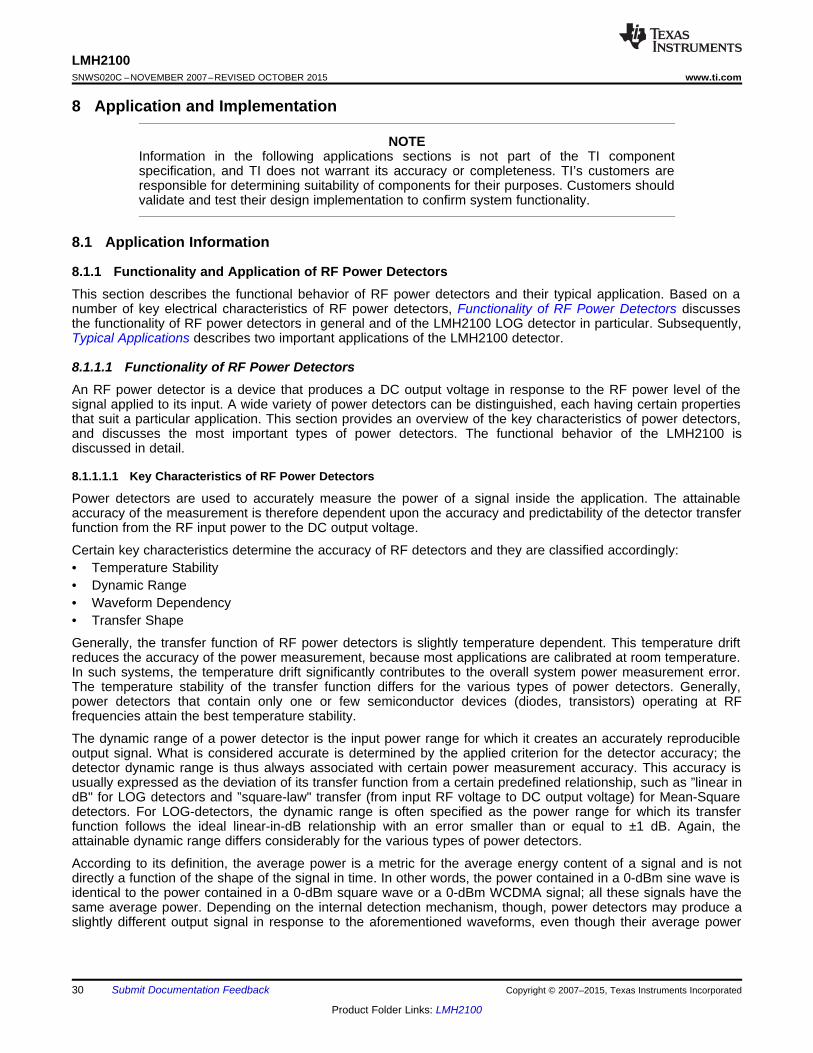
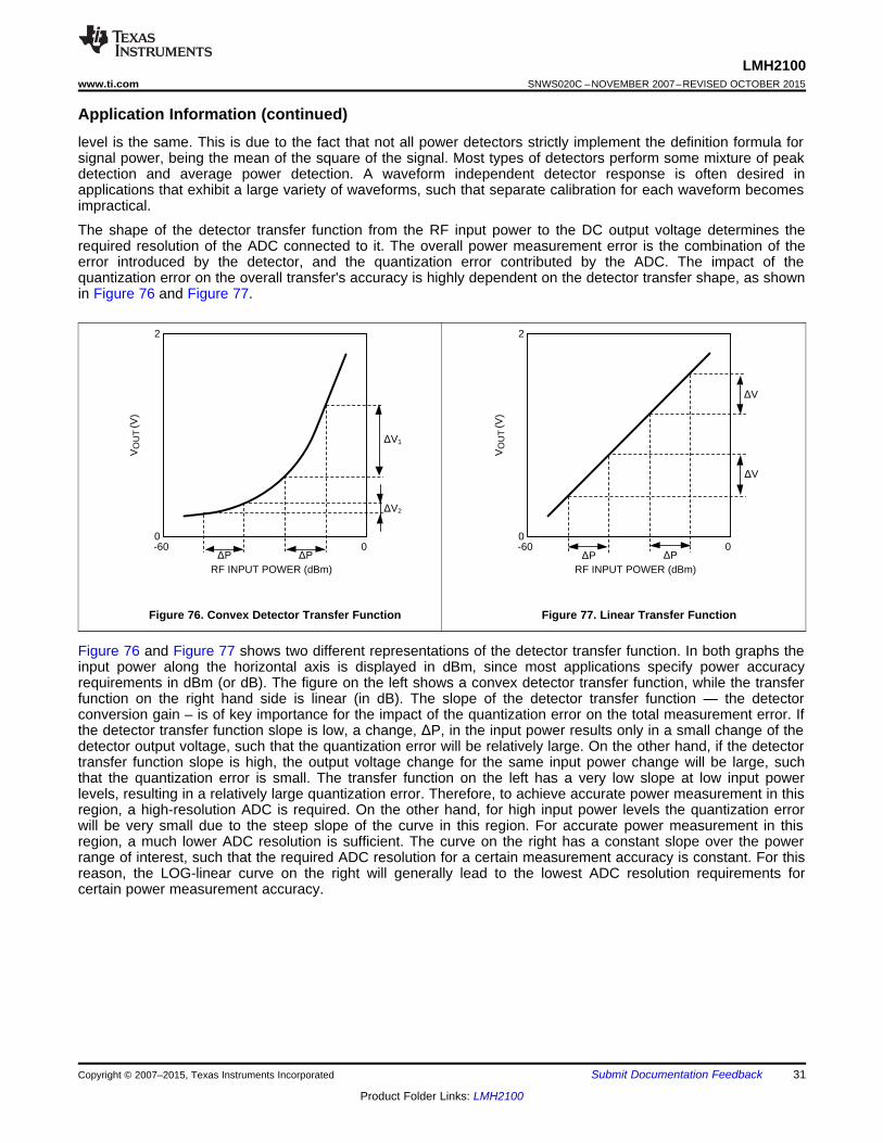
Application Information (continued)level is the same. This is due to the fact that not all power detectors strictly implement the definition formula forsignal power, being the mean of the square of the signal. Most types of detectors perform some mixture of peakdetection and average power detection. A waveform independent detector response is often desired inapplications that exhibit a large variety of waveforms, such that separate calibration for each waveform becomesimpractical.
The shape of the detector transfer function from the RF input power to the DC output voltage determines therequired resolution of the ADC connected to it. The overall power measurement error is the combination of theerror introduced by the detector, and the quantization error contributed by the ADC. The impact of thequantization error on the overall transfer's accuracy is highly dependent on the detector transfer shape, as shownin Figure 76 and Figure 77.
Figure 76. Convex Detector Transfer Function Figure 77. Linear Transfer Function
Figure 76 and Figure 77 shows two different representations of the detector transfer function. In both graphs theinput power along the horizontal axis is displayed in dBm, since most applications specify power accuracyrequirements in dBm (or dB). The figure on the left shows a convex detector transfer function, while the transferfunction on the right hand side is linear (in dB). The slope of the detector transfer function — the detectorconversion gain – is of key importance for the impact of the quantization error on the total measurement error. Ifthe detector transfer function slope is low, a change, ΔP, in the input power results only in a small change of thedetector output voltage, such that the quantization error will be relatively large. On the other hand, if the detectortransfer function slope is high, the output voltage change for the same input power change will be large, suchthat the quantization error is small. The transfer function on the left has a very low slope at low input powerlevels, resulting in a relatively large quantization error. Therefore, to achieve accurate power measurement in thisregion, a high-resolution ADC is required. On the other hand, for high input power levels the quantization errorwill be very small due to the steep slope of the curve in this region. For accurate power measurement in thisregion, a much lower ADC resolution is sufficient. The curve on the right has a constant slope over the powerrange of interest, such that the required ADC resolution for a certain measurement accuracy is constant. For thisreason, the LOG-linear curve on the right will generally lead to the lowest ADC resolution requirements forcertain power measurement accuracy.
Copyright © 2007–2015, Texas Instruments Incorporated Submit Documentation Feedback 31
Product Folder Links: LMH2100
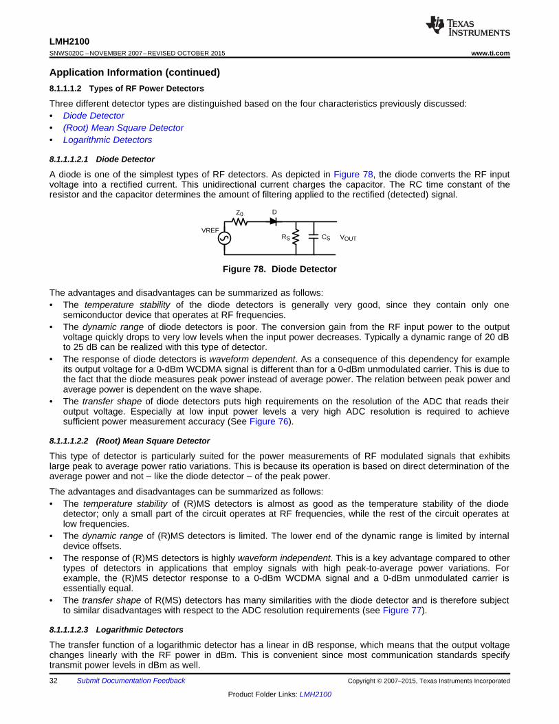
CSRS VOUT
Z0 D
VREF
LMH2100SNWS020C –NOVEMBER 2007–REVISED OCTOBER 2015 www.ti.com
Application Information (continued)8.1.1.1.2 Types of RF Power Detectors
Three different detector types are distinguished based on the four characteristics previously discussed:• Diode Detector• (Root) Mean Square Detector• Logarithmic Detectors
8.1.1.1.2.1 Diode Detector
A diode is one of the simplest types of RF detectors. As depicted in Figure 78, the diode converts the RF inputvoltage into a rectified current. This unidirectional current charges the capacitor. The RC time constant of theresistor and the capacitor determines the amount of filtering applied to the rectified (detected) signal.
Figure 78. Diode Detector
The advantages and disadvantages can be summarized as follows:• The temperature stability of the diode detectors is generally very good, since they contain only one
semiconductor device that operates at RF frequencies.• The dynamic range of diode detectors is poor. The conversion gain from the RF input power to the output
voltage quickly drops to very low levels when the input power decreases. Typically a dynamic range of 20 dBto 25 dB can be realized with this type of detector.
• The response of diode detectors is waveform dependent. As a consequence of this dependency for exampleits output voltage for a 0-dBm WCDMA signal is different than for a 0-dBm unmodulated carrier. This is due tothe fact that the diode measures peak power instead of average power. The relation between peak power andaverage power is dependent on the wave shape.
• The transfer shape of diode detectors puts high requirements on the resolution of the ADC that reads theiroutput voltage. Especially at low input power levels a very high ADC resolution is required to achievesufficient power measurement accuracy (See Figure 76).
8.1.1.1.2.2 (Root) Mean Square Detector
This type of detector is particularly suited for the power measurements of RF modulated signals that exhibitslarge peak to average power ratio variations. This is because its operation is based on direct determination of theaverage power and not – like the diode detector – of the peak power.
The advantages and disadvantages can be summarized as follows:• The temperature stability of (R)MS detectors is almost as good as the temperature stability of the diode
detector; only a small part of the circuit operates at RF frequencies, while the rest of the circuit operates atlow frequencies.
• The dynamic range of (R)MS detectors is limited. The lower end of the dynamic range is limited by internaldevice offsets.
• The response of (R)MS detectors is highly waveform independent. This is a key advantage compared to othertypes of detectors in applications that employ signals with high peak-to-average power variations. Forexample, the (R)MS detector response to a 0-dBm WCDMA signal and a 0-dBm unmodulated carrier isessentially equal.
• The transfer shape of R(MS) detectors has many similarities with the diode detector and is therefore subjectto similar disadvantages with respect to the ADC resolution requirements (see Figure 77).
8.1.1.1.2.3 Logarithmic Detectors
The transfer function of a logarithmic detector has a linear in dB response, which means that the output voltagechanges linearly with the RF power in dBm. This is convenient since most communication standards specifytransmit power levels in dBm as well.32 Submit Documentation Feedback Copyright © 2007–2015, Texas Instruments Incorporated
Product Folder Links: LMH2100
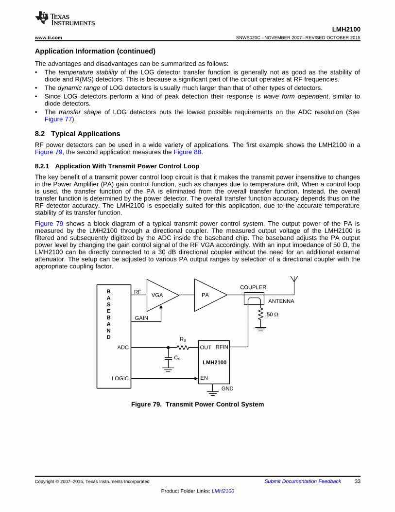
PAANTENNA
RFINOUT
LMH2100
RF
GND
50 :
EN
CS
RS
COUPLERVGA
BASEBAND
GAIN
ADC
LOGIC
LMH2100www.ti.com SNWS020C –NOVEMBER 2007–REVISED OCTOBER 2015
Application Information (continued)The advantages and disadvantages can be summarized as follows:• The temperature stability of the LOG detector transfer function is generally not as good as the stability of
diode and R(MS) detectors. This is because a significant part of the circuit operates at RF frequencies.• The dynamic range of LOG detectors is usually much larger than that of other types of detectors.• Since LOG detectors perform a kind of peak detection their response is wave form dependent, similar to
diode detectors.• The transfer shape of LOG detectors puts the lowest possible requirements on the ADC resolution (See
Figure 77).
8.2 Typical ApplicationsRF power detectors can be used in a wide variety of applications. The first example shows the LMH2100 in aFigure 79, the second application measures the Figure 88.
8.2.1 Application With Transmit Power Control LoopThe key benefit of a transmit power control loop circuit is that it makes the transmit power insensitive to changesin the Power Amplifier (PA) gain control function, such as changes due to temperature drift. When a control loopis used, the transfer function of the PA is eliminated from the overall transfer function. Instead, the overalltransfer function is determined by the power detector. The overall transfer function accuracy depends thus on theRF detector accuracy. The LMH2100 is especially suited for this application, due to the accurate temperaturestability of its transfer function.
Figure 79 shows a block diagram of a typical transmit power control system. The output power of the PA ismeasured by the LMH2100 through a directional coupler. The measured output voltage of the LMH2100 isfiltered and subsequently digitized by the ADC inside the baseband chip. The baseband adjusts the PA outputpower level by changing the gain control signal of the RF VGA accordingly. With an input impedance of 50 Ω, theLMH2100 can be directly connected to a 30 dB directional coupler without the need for an additional externalattenuator. The setup can be adjusted to various PA output ranges by selection of a directional coupler with theappropriate coupling factor.
Figure 79. Transmit Power Control System
Copyright © 2007–2015, Texas Instruments Incorporated Submit Documentation Feedback 33
Product Folder Links: LMH2100
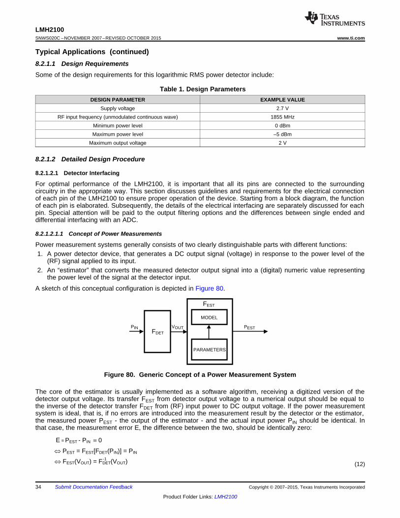
E = PEST - PIN 0
PEST = FEST[FDET(PIN)] = PIN
FEST(VOUT) = FDET(VOUT)-1
PIN PESTFDET
MODEL
PARAMETERS
VOUT
FEST
LMH2100SNWS020C –NOVEMBER 2007–REVISED OCTOBER 2015 www.ti.com
Typical Applications (continued)8.2.1.1 Design RequirementsSome of the design requirements for this logarithmic RMS power detector include:
Table 1. Design ParametersDESIGN PARAMETER EXAMPLE VALUE
Supply voltage 2.7 VRF input frequency (unmodulated continuous wave) 1855 MHz
Minimum power level 0 dBmMaximum power level –5 dBm
Maximum output voltage 2 V
8.2.1.2 Detailed Design Procedure
8.2.1.2.1 Detector Interfacing
For optimal performance of the LMH2100, it is important that all its pins are connected to the surroundingcircuitry in the appropriate way. This section discusses guidelines and requirements for the electrical connectionof each pin of the LMH2100 to ensure proper operation of the device. Starting from a block diagram, the functionof each pin is elaborated. Subsequently, the details of the electrical interfacing are separately discussed for eachpin. Special attention will be paid to the output filtering options and the differences between single ended anddifferential interfacing with an ADC.
8.2.1.2.1.1 Concept of Power Measurements
Power measurement systems generally consists of two clearly distinguishable parts with different functions:1. A power detector device, that generates a DC output signal (voltage) in response to the power level of the
(RF) signal applied to its input.2. An “estimator” that converts the measured detector output signal into a (digital) numeric value representing
the power level of the signal at the detector input.
A sketch of this conceptual configuration is depicted in Figure 80.
Figure 80. Generic Concept of a Power Measurement System
The core of the estimator is usually implemented as a software algorithm, receiving a digitized version of thedetector output voltage. Its transfer FEST from detector output voltage to a numerical output should be equal tothe inverse of the detector transfer FDET from (RF) input power to DC output voltage. If the power measurementsystem is ideal, that is, if no errors are introduced into the measurement result by the detector or the estimator,the measured power PEST - the output of the estimator - and the actual input power PIN should be identical. Inthat case, the measurement error E, the difference between the two, should be identically zero:
(12)
34 Submit Documentation Feedback Copyright © 2007–2015, Texas Instruments Incorporated
Product Folder Links: LMH2100
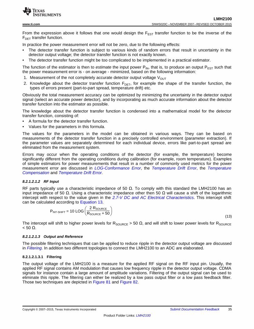
PINT-SHIFT = 10 LOG 2 RSOURCE
RSOURCE + 50¹·
©§
LMH2100www.ti.com SNWS020C –NOVEMBER 2007–REVISED OCTOBER 2015
From the expression above it follows that one would design the FEST transfer function to be the inverse of theFDET transfer function.
In practice the power measurement error will not be zero, due to the following effects:• The detector transfer function is subject to various kinds of random errors that result in uncertainty in the
detector output voltage; the detector transfer function is not exactly known.• The detector transfer function might be too complicated to be implemented in a practical estimator.
The function of the estimator is then to estimate the input power PIN, that is, to produce an output PEST such thatthe power measurement error is - on average - minimized, based on the following information:1. Measurement of the not completely accurate detector output voltage VOUT
2. Knowledge about the detector transfer function FDET, for example the shape of the transfer function, thetypes of errors present (part-to-part spread, temperature drift) etc.
Obviously the total measurement accuracy can be optimized by minimizing the uncertainty in the detector outputsignal (select an accurate power detector), and by incorporating as much accurate information about the detectortransfer function into the estimator as possible.
The knowledge about the detector transfer function is condensed into a mathematical model for the detectortransfer function, consisting of:• A formula for the detector transfer function.• Values for the parameters in this formula.
The values for the parameters in the model can be obtained in various ways. They can be based onmeasurements of the detector transfer function in a precisely controlled environment (parameter extraction). Ifthe parameter values are separately determined for each individual device, errors like part-to-part spread areeliminated from the measurement system.
Errors may occur when the operating conditions of the detector (for example, the temperature) becomesignificantly different from the operating conditions during calibration (for example, room temperature). Examplesof simple estimators for power measurements that result in a number of commonly used metrics for the powermeasurement error are discussed in LOG-Conformance Error, the Temperature Drift Error, the TemperatureCompensation and Temperature Drift Error.
8.2.1.2.1.2 RF Input
RF parts typically use a characteristic impedance of 50 Ω. To comply with this standard the LMH2100 has aninput impedance of 50 Ω. Using a characteristic impedance other then 50 Ω will cause a shift of the logarithmicintercept with respect to the value given in the 2.7-V DC and AC Electrical Characteristics. This intercept shiftcan be calculated according to Equation 13.
(13)
The intercept will shift to higher power levels for RSOURCE > 50 Ω, and will shift to lower power levels for RSOURCE< 50 Ω.
8.2.1.2.1.3 Output and Reference
The possible filtering techniques that can be applied to reduce ripple in the detector output voltage are discussedin Filtering. In addition two different topologies to connect the LMH2100 to an ADC are elaborated.
8.2.1.2.1.3.1 Filtering
The output voltage of the LMH2100 is a measure for the applied RF signal on the RF input pin. Usually, theapplied RF signal contains AM modulation that causes low frequency ripple in the detector output voltage. CDMAsignals for instance contain a large amount of amplitude variations. Filtering of the output signal can be used toeliminate this ripple. The filtering can either be realized by a low pass output filter or a low pass feedback filter.Those two techniques are depicted in Figure 81 and Figure 82.
Copyright © 2007–2015, Texas Instruments Incorporated Submit Documentation Feedback 35
Product Folder Links: LMH2100
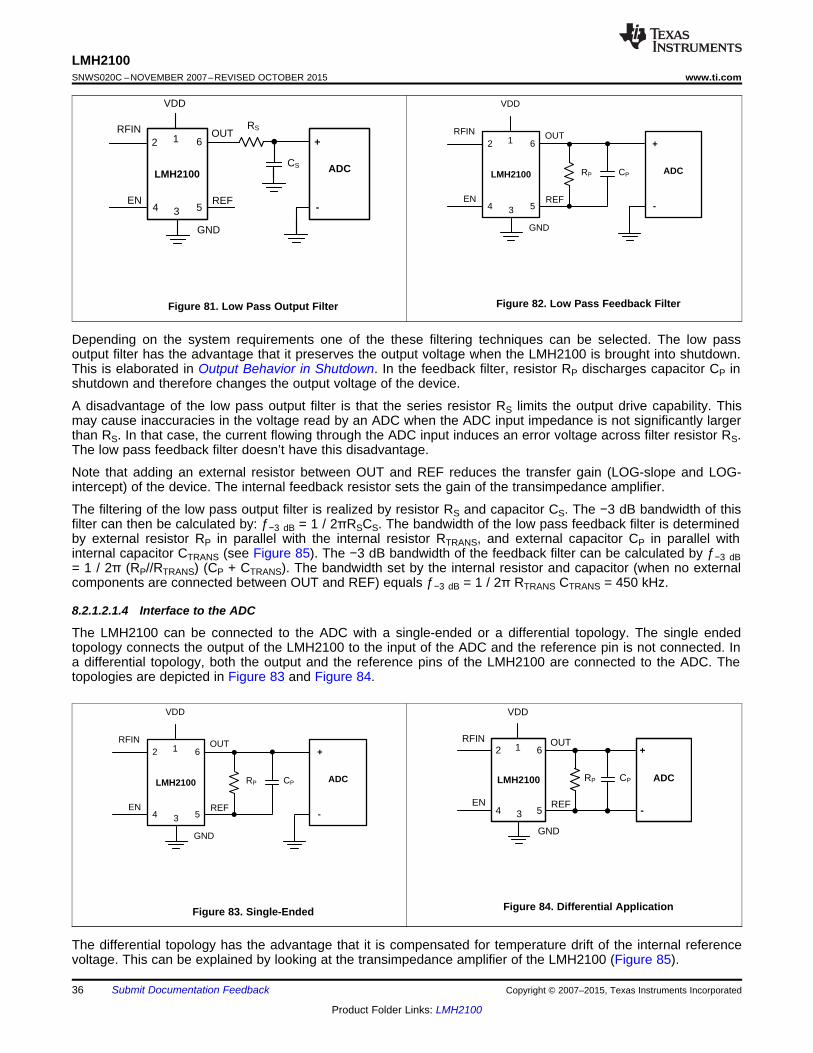
RFIN OUT
LMH2100
VDD
GND
EN REF
ADC
2
CPRP
1 6
34 5 -
+RFIN OUT
LMH2100
VDD
GND
EN REF
ADC
2
CPRP
1 6
34 5 -
+
RFIN OUT
LMH2100
VDD
GND
EN REF
ADC
2
CS
RS
1 6
34 5 -
+RFIN OUT
LMH2100
VDD
GND
EN REF
ADC
2
CPRP
1 6
34 5 -
+
LMH2100SNWS020C –NOVEMBER 2007–REVISED OCTOBER 2015 www.ti.com
Figure 82. Low Pass Feedback FilterFigure 81. Low Pass Output Filter
Depending on the system requirements one of the these filtering techniques can be selected. The low passoutput filter has the advantage that it preserves the output voltage when the LMH2100 is brought into shutdown.This is elaborated in Output Behavior in Shutdown. In the feedback filter, resistor RP discharges capacitor CP inshutdown and therefore changes the output voltage of the device.
A disadvantage of the low pass output filter is that the series resistor RS limits the output drive capability. Thismay cause inaccuracies in the voltage read by an ADC when the ADC input impedance is not significantly largerthan RS. In that case, the current flowing through the ADC input induces an error voltage across filter resistor RS.The low pass feedback filter doesn’t have this disadvantage.
Note that adding an external resistor between OUT and REF reduces the transfer gain (LOG-slope and LOG-intercept) of the device. The internal feedback resistor sets the gain of the transimpedance amplifier.
The filtering of the low pass output filter is realized by resistor RS and capacitor CS. The −3 dB bandwidth of thisfilter can then be calculated by: ƒ−3 dB = 1 / 2πRSCS. The bandwidth of the low pass feedback filter is determinedby external resistor RP in parallel with the internal resistor RTRANS, and external capacitor CP in parallel withinternal capacitor CTRANS (see Figure 85). The −3 dB bandwidth of the feedback filter can be calculated by ƒ−3 dB= 1 / 2π (RP//RTRANS) (CP + CTRANS). The bandwidth set by the internal resistor and capacitor (when no externalcomponents are connected between OUT and REF) equals ƒ−3 dB = 1 / 2π RTRANS CTRANS = 450 kHz.
8.2.1.2.1.4 Interface to the ADC
The LMH2100 can be connected to the ADC with a single-ended or a differential topology. The single endedtopology connects the output of the LMH2100 to the input of the ADC and the reference pin is not connected. Ina differential topology, both the output and the reference pins of the LMH2100 are connected to the ADC. Thetopologies are depicted in Figure 83 and Figure 84.
Figure 84. Differential ApplicationFigure 83. Single-Ended
The differential topology has the advantage that it is compensated for temperature drift of the internal referencevoltage. This can be explained by looking at the transimpedance amplifier of the LMH2100 (Figure 85).
36 Submit Documentation Feedback Copyright © 2007–2015, Texas Instruments Incorporated
Product Folder Links: LMH2100
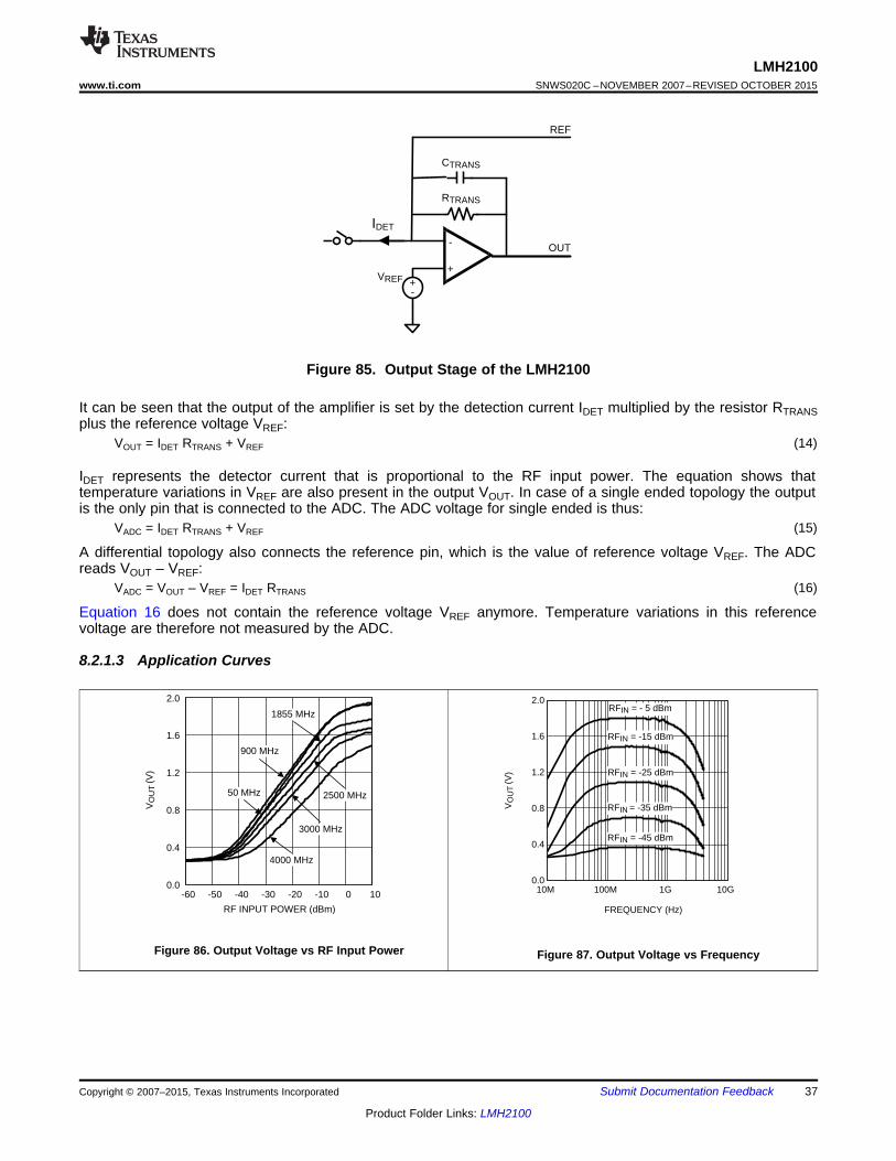
FREQUENCY (Hz)
VO
UT
(V)
2.0
1.6
1.2
0.8
0.4
0.010M 100M 1G 10G
RFIN = -45 dBm
RFIN = -35 dBm
RFIN = -25 dBm
RFIN = -15 dBm
RFIN = - 5 dBm
RF INPUT POWER (dBm)
VO
UT
(V)
2.0
1.6
1.2
0.8
0.4
0.0
-60 -50 -40 -30 -20 -10 0 10
50 MHz
3000 MHz
900 MHz
1855 MHz
2500 MHz
4000 MHz
2.0
1.6
1.2
0.8
0.4
0.0
OUT-
+
REF
VREF +-
IDET
RTRANS
CTRANS
LMH2100www.ti.com SNWS020C –NOVEMBER 2007–REVISED OCTOBER 2015
Figure 85. Output Stage of the LMH2100
It can be seen that the output of the amplifier is set by the detection current IDET multiplied by the resistor RTRANSplus the reference voltage VREF:
VOUT = IDET RTRANS + VREF (14)
IDET represents the detector current that is proportional to the RF input power. The equation shows thattemperature variations in VREF are also present in the output VOUT. In case of a single ended topology the outputis the only pin that is connected to the ADC. The ADC voltage for single ended is thus:
VADC = IDET RTRANS + VREF (15)
A differential topology also connects the reference pin, which is the value of reference voltage VREF. The ADCreads VOUT – VREF:
VADC = VOUT – VREF = IDET RTRANS (16)
Equation 16 does not contain the reference voltage VREF anymore. Temperature variations in this referencevoltage are therefore not measured by the ADC.
8.2.1.3 Application Curves
Figure 86. Output Voltage vs RF Input Power Figure 87. Output Voltage vs Frequency
Copyright © 2007–2015, Texas Instruments Incorporated Submit Documentation Feedback 37
Product Folder Links: LMH2100
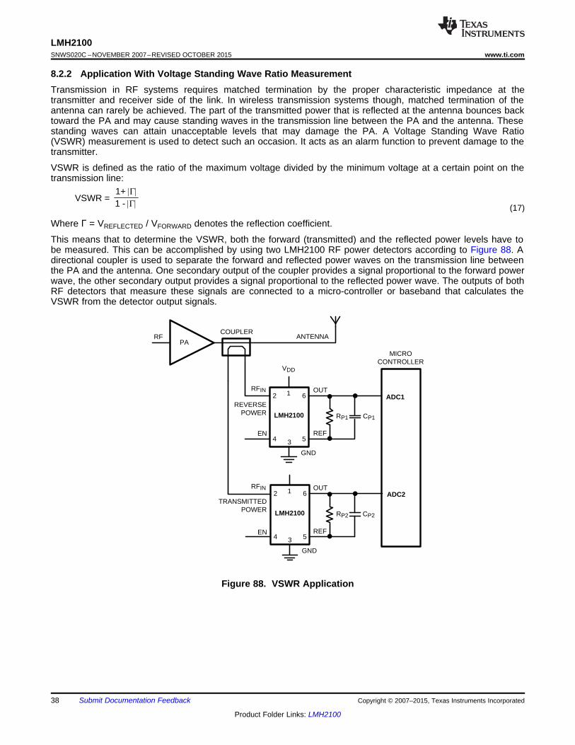
PAANTENNA
RFIN OUT
LMH2100
RF
VDD
GND
REF
ADC12
CP1RP1
1 6
34 5
COUPLER
EN
RFIN OUT
LMH2100
GND
REF
ADC22
CP2RP2
1 6
34 5EN
MICRO CONTROLLER
REVERSE POWER
TRANSMITTED POWER
VSWR =1+_*_
1 - _*_
LMH2100SNWS020C –NOVEMBER 2007–REVISED OCTOBER 2015 www.ti.com
8.2.2 Application With Voltage Standing Wave Ratio MeasurementTransmission in RF systems requires matched termination by the proper characteristic impedance at thetransmitter and receiver side of the link. In wireless transmission systems though, matched termination of theantenna can rarely be achieved. The part of the transmitted power that is reflected at the antenna bounces backtoward the PA and may cause standing waves in the transmission line between the PA and the antenna. Thesestanding waves can attain unacceptable levels that may damage the PA. A Voltage Standing Wave Ratio(VSWR) measurement is used to detect such an occasion. It acts as an alarm function to prevent damage to thetransmitter.
VSWR is defined as the ratio of the maximum voltage divided by the minimum voltage at a certain point on thetransmission line:
(17)
Where Γ = VREFLECTED / VFORWARD denotes the reflection coefficient.
This means that to determine the VSWR, both the forward (transmitted) and the reflected power levels have tobe measured. This can be accomplished by using two LMH2100 RF power detectors according to Figure 88. Adirectional coupler is used to separate the forward and reflected power waves on the transmission line betweenthe PA and the antenna. One secondary output of the coupler provides a signal proportional to the forward powerwave, the other secondary output provides a signal proportional to the reflected power wave. The outputs of bothRF detectors that measure these signals are connected to a micro-controller or baseband that calculates theVSWR from the detector output signals.
Figure 88. VSWR Application
38 Submit Documentation Feedback Copyright © 2007–2015, Texas Instruments Incorporated
Product Folder Links: LMH2100

LMH2100www.ti.com SNWS020C –NOVEMBER 2007–REVISED OCTOBER 2015
9 Power Supply RecommendationsThe LMH2100 is designed to operate from an input voltage supply range between 2.7 V to 3.3 V. This inputvoltage must be well regulated. Enable voltage levels lower than 400 below GND could lead to incorrectoperation of the device. Also, the resistance of the input supply rail must be low enough to ensure correctoperation of the device.
Copyright © 2007–2015, Texas Instruments Incorporated Submit Documentation Feedback 39
Product Folder Links: LMH2100

LMH2100SNWS020C –NOVEMBER 2007–REVISED OCTOBER 2015 www.ti.com
10 Layout
10.1 Layout GuidelinesAs with any other RF device, careful attention must be paid to the board layout. If the board layout is not properlydesigned, unwanted signals can easily be detected or interference will be picked up. This section givesguidelines for proper board layout for the LMH2100.
Electrical signals (voltages and currents) need a finite time to travel through a trace or transmission line. RFvoltage levels at the generator side and at the detector side can therefore be different. This is not only true forthe RF strip line, but for all traces on the PCB. Signals at different locations or traces on the PCB will be in adifferent phase of the RF frequency cycle. Phase differences in, for example, the voltage across neighboringlines, may result in crosstalk between lines due to parasitic capacitive or inductive coupling. This crosstalk isfurther enhanced by the fact that all traces on the PCB are susceptible to resonance. The resonance frequencydepends on the trace geometry. Traces are particularly sensitive to interference when the length of the tracecorresponds to a quarter of the wavelength of the interfering signal or a multiple thereof.
10.1.1 Supply LinesBecause the PSRR of the LMH2100 is finite, variations of the supply can result in some variation at the output.This can be caused among others by RF injection from other parts of the circuitry or the on/off switching of thePA.
10.1.1.1 Positive Supply (VDD)In order to minimize the injection of RF interference into the LMH2100 through the supply lines, the phasedifference between the PCB traces connecting to VDD and GND should be minimized. A suitable way to achievethis is to short both connections for RF. This can be done by placing a small decoupling capacitor between theVDD and GND. It should be placed as close as possible to the VDD and GND pins of the LMH2100 as indicatedin Figure 91. Be aware that the resonance frequency of the capacitor itself should be above the highest RFfrequency used in the application, because the capacitor acts as an inductor above its resonance frequency.
Low frequency supply voltage variations due to PA switching might result in a ripple at the output voltage. TheLMH2100 has a PSRR of 60 dB for low frequencies.
10.1.1.2 Ground (GND)The LMH2100 needs a ground plane free of noise and other disturbing signals. It is important to separate the RFground return path from the other grounds. This is due to the fact that the RF input handles large voltage swings.A power level of 0 dBm will cause a voltage swing larger than 0.6 VPP, over the internal 50-Ω input resistor. Thiswill result in a significant RF return current toward the source. It is therefore recommended that the RF groundreturn path not be used for other circuits in the design. The RF path should be routed directly back to the sourcewithout loops.
10.1.2 RF Input InterfaceThe LMH2100 is designed to be used in RF applications, having a characteristic impedance of 50Ω. To achievethis impedance, the input of the LMH2100 needs to be connected via a 50Ω transmission line. Transmission linescan be easily created on PCBs using microstrip or (grounded) coplanar waveguide (GCPW) configurations. Thissection will discuss both configurations in a general way. For more details about designing microstrip or GCPWtransmission lines, a microwave designer handbook is recommended.
10.1.3 Microstrip ConfigurationOne way to create a transmission line is to use a microstrip configuration. A cross section of the configuration isshown in Figure 89, assuming a two-layer PCB.
40 Submit Documentation Feedback Copyright © 2007–2015, Texas Instruments Incorporated
Product Folder Links: LMH2100
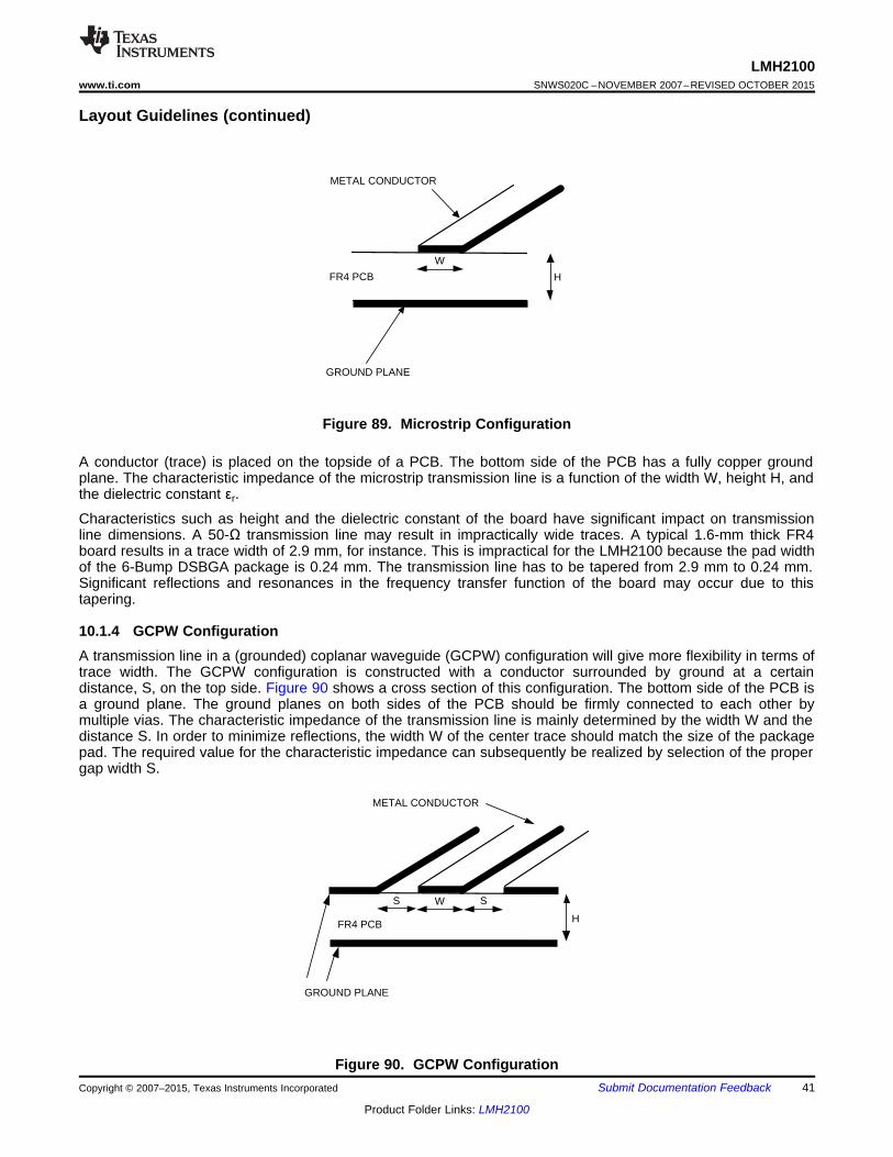
W
GROUND PLANE
METAL CONDUCTOR
FR4 PCB
SS
H
W
H
GROUND PLANE
METAL CONDUCTOR
FR4 PCB
LMH2100www.ti.com SNWS020C –NOVEMBER 2007–REVISED OCTOBER 2015
Layout Guidelines (continued)
Figure 89. Microstrip Configuration
A conductor (trace) is placed on the topside of a PCB. The bottom side of the PCB has a fully copper groundplane. The characteristic impedance of the microstrip transmission line is a function of the width W, height H, andthe dielectric constant εr.
Characteristics such as height and the dielectric constant of the board have significant impact on transmissionline dimensions. A 50-Ω transmission line may result in impractically wide traces. A typical 1.6-mm thick FR4board results in a trace width of 2.9 mm, for instance. This is impractical for the LMH2100 because the pad widthof the 6-Bump DSBGA package is 0.24 mm. The transmission line has to be tapered from 2.9 mm to 0.24 mm.Significant reflections and resonances in the frequency transfer function of the board may occur due to thistapering.
10.1.4 GCPW ConfigurationA transmission line in a (grounded) coplanar waveguide (GCPW) configuration will give more flexibility in terms oftrace width. The GCPW configuration is constructed with a conductor surrounded by ground at a certaindistance, S, on the top side. Figure 90 shows a cross section of this configuration. The bottom side of the PCB isa ground plane. The ground planes on both sides of the PCB should be firmly connected to each other bymultiple vias. The characteristic impedance of the transmission line is mainly determined by the width W and thedistance S. In order to minimize reflections, the width W of the center trace should match the size of the packagepad. The required value for the characteristic impedance can subsequently be realized by selection of the propergap width S.
Figure 90. GCPW ConfigurationCopyright © 2007–2015, Texas Instruments Incorporated Submit Documentation Feedback 41
Product Folder Links: LMH2100
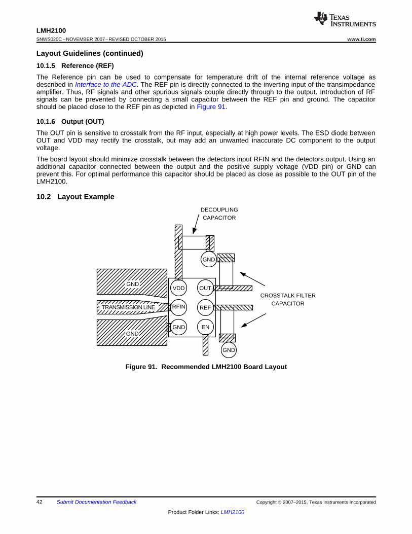
DECOUPLINGCAPACITOR
REF
ENGND
CROSSTALK FILTERCAPACITOR
OUT
GND
GND
TRANSMISSION LINE
VDD
GND
GND
RFIN
LMH2100SNWS020C –NOVEMBER 2007–REVISED OCTOBER 2015 www.ti.com
Layout Guidelines (continued)10.1.5 Reference (REF)The Reference pin can be used to compensate for temperature drift of the internal reference voltage asdescribed in Interface to the ADC. The REF pin is directly connected to the inverting input of the transimpedanceamplifier. Thus, RF signals and other spurious signals couple directly through to the output. Introduction of RFsignals can be prevented by connecting a small capacitor between the REF pin and ground. The capacitorshould be placed close to the REF pin as depicted in Figure 91.
10.1.6 Output (OUT)The OUT pin is sensitive to crosstalk from the RF input, especially at high power levels. The ESD diode betweenOUT and VDD may rectify the crosstalk, but may add an unwanted inaccurate DC component to the outputvoltage.
The board layout should minimize crosstalk between the detectors input RFIN and the detectors output. Using anadditional capacitor connected between the output and the positive supply voltage (VDD pin) or GND canprevent this. For optimal performance this capacitor should be placed as close as possible to the OUT pin of theLMH2100.
10.2 Layout Example
Figure 91. Recommended LMH2100 Board Layout
42 Submit Documentation Feedback Copyright © 2007–2015, Texas Instruments Incorporated
Product Folder Links: LMH2100

LMH2100www.ti.com SNWS020C –NOVEMBER 2007–REVISED OCTOBER 2015
11 Device and Documentation Support
11.1 Community ResourcesThe following links connect to TI community resources. Linked contents are provided "AS IS" by the respectivecontributors. They do not constitute TI specifications and do not necessarily reflect TI's views; see TI's Terms ofUse.
TI E2E™ Online Community TI's Engineer-to-Engineer (E2E) Community. Created to foster collaborationamong engineers. At e2e.ti.com, you can ask questions, share knowledge, explore ideas and helpsolve problems with fellow engineers.
Design Support TI's Design Support Quickly find helpful E2E forums along with design support tools andcontact information for technical support.
11.2 TrademarksE2E is a trademark of Texas Instruments.All other trademarks are the property of their respective owners.
11.3 Electrostatic Discharge CautionThis integrated circuit can be damaged by ESD. Texas Instruments recommends that all integrated circuits be handled withappropriate precautions. Failure to observe proper handling and installation procedures can cause damage.
ESD damage can range from subtle performance degradation to complete device failure. Precision integrated circuits may be moresusceptible to damage because very small parametric changes could cause the device not to meet its published specifications.
11.4 GlossarySLYZ022 — TI Glossary.
This glossary lists and explains terms, acronyms, and definitions.
12 Mechanical, Packaging, and Orderable InformationThe following pages include mechanical, packaging, and orderable information. This information is the mostcurrent data available for the designated devices. This data is subject to change without notice and revision ofthis document. For browser-based versions of this data sheet, refer to the left-hand navigation.
Copyright © 2007–2015, Texas Instruments Incorporated Submit Documentation Feedback 43
Product Folder Links: LMH2100
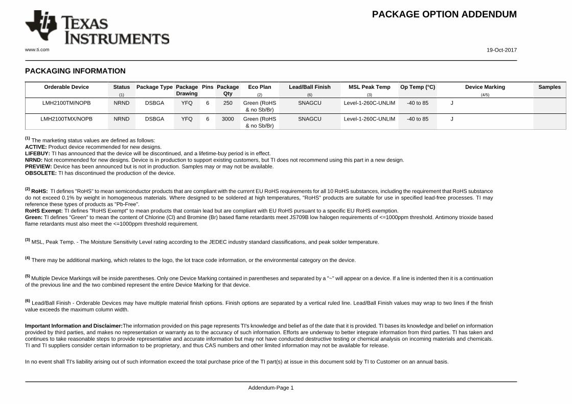
PACKAGE OPTION ADDENDUM
www.ti.com 19-Oct-2017
Addendum-Page 1
PACKAGING INFORMATION
Orderable Device Status(1)
Package Type PackageDrawing
Pins PackageQty
Eco Plan(2)
Lead/Ball Finish(6)
MSL Peak Temp(3)
Op Temp (°C) Device Marking(4/5)
Samples
LMH2100TM/NOPB NRND DSBGA YFQ 6 250 Green (RoHS& no Sb/Br)
SNAGCU Level-1-260C-UNLIM -40 to 85 J
LMH2100TMX/NOPB NRND DSBGA YFQ 6 3000 Green (RoHS& no Sb/Br)
SNAGCU Level-1-260C-UNLIM -40 to 85 J
(1) The marketing status values are defined as follows:ACTIVE: Product device recommended for new designs.LIFEBUY: TI has announced that the device will be discontinued, and a lifetime-buy period is in effect.NRND: Not recommended for new designs. Device is in production to support existing customers, but TI does not recommend using this part in a new design.PREVIEW: Device has been announced but is not in production. Samples may or may not be available.OBSOLETE: TI has discontinued the production of the device.
(2) RoHS: TI defines "RoHS" to mean semiconductor products that are compliant with the current EU RoHS requirements for all 10 RoHS substances, including the requirement that RoHS substancedo not exceed 0.1% by weight in homogeneous materials. Where designed to be soldered at high temperatures, "RoHS" products are suitable for use in specified lead-free processes. TI mayreference these types of products as "Pb-Free".RoHS Exempt: TI defines "RoHS Exempt" to mean products that contain lead but are compliant with EU RoHS pursuant to a specific EU RoHS exemption.Green: TI defines "Green" to mean the content of Chlorine (Cl) and Bromine (Br) based flame retardants meet JS709B low halogen requirements of <=1000ppm threshold. Antimony trioxide basedflame retardants must also meet the <=1000ppm threshold requirement.
(3) MSL, Peak Temp. - The Moisture Sensitivity Level rating according to the JEDEC industry standard classifications, and peak solder temperature.
(4) There may be additional marking, which relates to the logo, the lot trace code information, or the environmental category on the device.
(5) Multiple Device Markings will be inside parentheses. Only one Device Marking contained in parentheses and separated by a "~" will appear on a device. If a line is indented then it is a continuationof the previous line and the two combined represent the entire Device Marking for that device.
(6) Lead/Ball Finish - Orderable Devices may have multiple material finish options. Finish options are separated by a vertical ruled line. Lead/Ball Finish values may wrap to two lines if the finishvalue exceeds the maximum column width.
Important Information and Disclaimer:The information provided on this page represents TI's knowledge and belief as of the date that it is provided. TI bases its knowledge and belief on informationprovided by third parties, and makes no representation or warranty as to the accuracy of such information. Efforts are underway to better integrate information from third parties. TI has taken andcontinues to take reasonable steps to provide representative and accurate information but may not have conducted destructive testing or chemical analysis on incoming materials and chemicals.TI and TI suppliers consider certain information to be proprietary, and thus CAS numbers and other limited information may not be available for release.
In no event shall TI's liability arising out of such information exceed the total purchase price of the TI part(s) at issue in this document sold by TI to Customer on an annual basis.

PACKAGE OPTION ADDENDUM
www.ti.com 19-Oct-2017
Addendum-Page 2
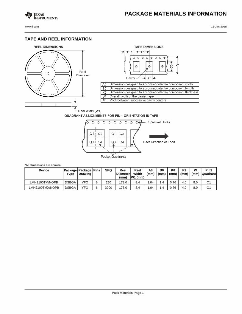
TAPE AND REEL INFORMATION
*All dimensions are nominal
Device PackageType
PackageDrawing
Pins SPQ ReelDiameter
(mm)
ReelWidth
W1 (mm)
A0(mm)
B0(mm)
K0(mm)
P1(mm)
W(mm)
Pin1Quadrant
LMH2100TM/NOPB DSBGA YFQ 6 250 178.0 8.4 1.04 1.4 0.76 4.0 8.0 Q1
LMH2100TMX/NOPB DSBGA YFQ 6 3000 178.0 8.4 1.04 1.4 0.76 4.0 8.0 Q1
PACKAGE MATERIALS INFORMATION
www.ti.com 18-Jan-2018
Pack Materials-Page 1

*All dimensions are nominal
Device Package Type Package Drawing Pins SPQ Length (mm) Width (mm) Height (mm)
LMH2100TM/NOPB DSBGA YFQ 6 250 210.0 185.0 35.0
LMH2100TMX/NOPB DSBGA YFQ 6 3000 210.0 185.0 35.0
PACKAGE MATERIALS INFORMATION
www.ti.com 18-Jan-2018
Pack Materials-Page 2
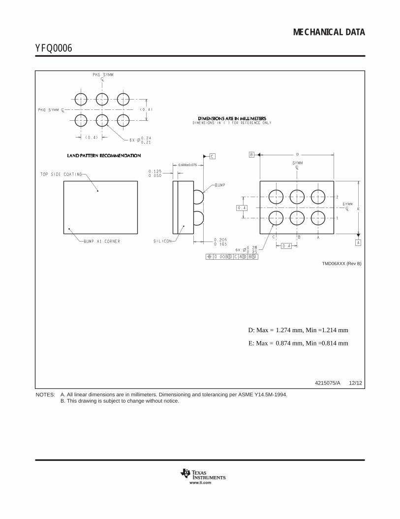
MECHANICAL DATA
YFQ0006xxx
www.ti.com
TMD06XXX (Rev B)
E
0.600±0.075
D
A. All linear dimensions are in millimeters. Dimensioning and tolerancing per ASME Y14.5M-1994.B. This drawing is subject to change without notice.
NOTES:
4215075/A 12/12
D: Max =
E: Max =
1.274 mm, Min =
0.874 mm, Min =
1.214 mm
0.814 mm

IMPORTANT NOTICE
Texas Instruments Incorporated (TI) reserves the right to make corrections, enhancements, improvements and other changes to itssemiconductor products and services per JESD46, latest issue, and to discontinue any product or service per JESD48, latest issue. Buyersshould obtain the latest relevant information before placing orders and should verify that such information is current and complete.TI’s published terms of sale for semiconductor products (http://www.ti.com/sc/docs/stdterms.htm) apply to the sale of packaged integratedcircuit products that TI has qualified and released to market. Additional terms may apply to the use or sale of other types of TI products andservices.Reproduction of significant portions of TI information in TI data sheets is permissible only if reproduction is without alteration and isaccompanied by all associated warranties, conditions, limitations, and notices. TI is not responsible or liable for such reproduceddocumentation. Information of third parties may be subject to additional restrictions. Resale of TI products or services with statementsdifferent from or beyond the parameters stated by TI for that product or service voids all express and any implied warranties for theassociated TI product or service and is an unfair and deceptive business practice. TI is not responsible or liable for any such statements.Buyers and others who are developing systems that incorporate TI products (collectively, “Designers”) understand and agree that Designersremain responsible for using their independent analysis, evaluation and judgment in designing their applications and that Designers havefull and exclusive responsibility to assure the safety of Designers' applications and compliance of their applications (and of all TI productsused in or for Designers’ applications) with all applicable regulations, laws and other applicable requirements. Designer represents that, withrespect to their applications, Designer has all the necessary expertise to create and implement safeguards that (1) anticipate dangerousconsequences of failures, (2) monitor failures and their consequences, and (3) lessen the likelihood of failures that might cause harm andtake appropriate actions. Designer agrees that prior to using or distributing any applications that include TI products, Designer willthoroughly test such applications and the functionality of such TI products as used in such applications.TI’s provision of technical, application or other design advice, quality characterization, reliability data or other services or information,including, but not limited to, reference designs and materials relating to evaluation modules, (collectively, “TI Resources”) are intended toassist designers who are developing applications that incorporate TI products; by downloading, accessing or using TI Resources in anyway, Designer (individually or, if Designer is acting on behalf of a company, Designer’s company) agrees to use any particular TI Resourcesolely for this purpose and subject to the terms of this Notice.TI’s provision of TI Resources does not expand or otherwise alter TI’s applicable published warranties or warranty disclaimers for TIproducts, and no additional obligations or liabilities arise from TI providing such TI Resources. TI reserves the right to make corrections,enhancements, improvements and other changes to its TI Resources. TI has not conducted any testing other than that specificallydescribed in the published documentation for a particular TI Resource.Designer is authorized to use, copy and modify any individual TI Resource only in connection with the development of applications thatinclude the TI product(s) identified in such TI Resource. NO OTHER LICENSE, EXPRESS OR IMPLIED, BY ESTOPPEL OR OTHERWISETO ANY OTHER TI INTELLECTUAL PROPERTY RIGHT, AND NO LICENSE TO ANY TECHNOLOGY OR INTELLECTUAL PROPERTYRIGHT OF TI OR ANY THIRD PARTY IS GRANTED HEREIN, including but not limited to any patent right, copyright, mask work right, orother intellectual property right relating to any combination, machine, or process in which TI products or services are used. Informationregarding or referencing third-party products or services does not constitute a license to use such products or services, or a warranty orendorsement thereof. Use of TI Resources may require a license from a third party under the patents or other intellectual property of thethird party, or a license from TI under the patents or other intellectual property of TI.TI RESOURCES ARE PROVIDED “AS IS” AND WITH ALL FAULTS. TI DISCLAIMS ALL OTHER WARRANTIES ORREPRESENTATIONS, EXPRESS OR IMPLIED, REGARDING RESOURCES OR USE THEREOF, INCLUDING BUT NOT LIMITED TOACCURACY OR COMPLETENESS, TITLE, ANY EPIDEMIC FAILURE WARRANTY AND ANY IMPLIED WARRANTIES OFMERCHANTABILITY, FITNESS FOR A PARTICULAR PURPOSE, AND NON-INFRINGEMENT OF ANY THIRD PARTY INTELLECTUALPROPERTY RIGHTS. TI SHALL NOT BE LIABLE FOR AND SHALL NOT DEFEND OR INDEMNIFY DESIGNER AGAINST ANY CLAIM,INCLUDING BUT NOT LIMITED TO ANY INFRINGEMENT CLAIM THAT RELATES TO OR IS BASED ON ANY COMBINATION OFPRODUCTS EVEN IF DESCRIBED IN TI RESOURCES OR OTHERWISE. IN NO EVENT SHALL TI BE LIABLE FOR ANY ACTUAL,DIRECT, SPECIAL, COLLATERAL, INDIRECT, PUNITIVE, INCIDENTAL, CONSEQUENTIAL OR EXEMPLARY DAMAGES INCONNECTION WITH OR ARISING OUT OF TI RESOURCES OR USE THEREOF, AND REGARDLESS OF WHETHER TI HAS BEENADVISED OF THE POSSIBILITY OF SUCH DAMAGES.Unless TI has explicitly designated an individual product as meeting the requirements of a particular industry standard (e.g., ISO/TS 16949and ISO 26262), TI is not responsible for any failure to meet such industry standard requirements.Where TI specifically promotes products as facilitating functional safety or as compliant with industry functional safety standards, suchproducts are intended to help enable customers to design and create their own applications that meet applicable functional safety standardsand requirements. Using products in an application does not by itself establish any safety features in the application. Designers mustensure compliance with safety-related requirements and standards applicable to their applications. Designer may not use any TI products inlife-critical medical equipment unless authorized officers of the parties have executed a special contract specifically governing such use.Life-critical medical equipment is medical equipment where failure of such equipment would cause serious bodily injury or death (e.g., lifesupport, pacemakers, defibrillators, heart pumps, neurostimulators, and implantables). Such equipment includes, without limitation, allmedical devices identified by the U.S. Food and Drug Administration as Class III devices and equivalent classifications outside the U.S.TI may expressly designate certain products as completing a particular qualification (e.g., Q100, Military Grade, or Enhanced Product).Designers agree that it has the necessary expertise to select the product with the appropriate qualification designation for their applicationsand that proper product selection is at Designers’ own risk. Designers are solely responsible for compliance with all legal and regulatoryrequirements in connection with such selection.Designer will fully indemnify TI and its representatives against any damages, costs, losses, and/or liabilities arising out of Designer’s non-compliance with the terms and provisions of this Notice.
Mailing Address: Texas Instruments, Post Office Box 655303, Dallas, Texas 75265Copyright © 2018, Texas Instruments Incorporated


![TW AUDiO Presets KDSP Preset guide EN 1 · 10 dB -S dB -10 dB -20 dB — -25 dB -30 dB -40 dB O dB MUTE Options Magnitude [-12 12] Layer I 16Hz Layer 2 Layer 3 Delay ms 1.715 m -12d8](https://img.dokumen.tips/doc/110x75/60d3e9cc1ee64b29d6441834/tw-audio-presets-kdsp-preset-guide-en-1-10-db-s-db-10-db-20-db-a-25-db-30.jpg)


![Untitled-1 []...Klipsch RP- 160M 100 Hz f 10 dB '00 dB 90 dB 70 dB Klipsch 160M Pegel- & Klirrverlauf — dB 90 dB — dB — 100 dB 16 Ohm 8 Ohm 2 Ohm 1 Ohm kHz 40 kHz dB 50 dB 20](https://img.dokumen.tips/doc/110x75/60961ba59437253425333804/untitled-1-klipsch-rp-160m-100-hz-f-10-db-00-db-90-db-70-db-klipsch-160m.jpg)