Embed Size (px)
Citation preview
Lecture: Solid State Chemistry(Festkörperchemie)
Part 1
H.J. Deiseroth, SS 2006

Resources Resources
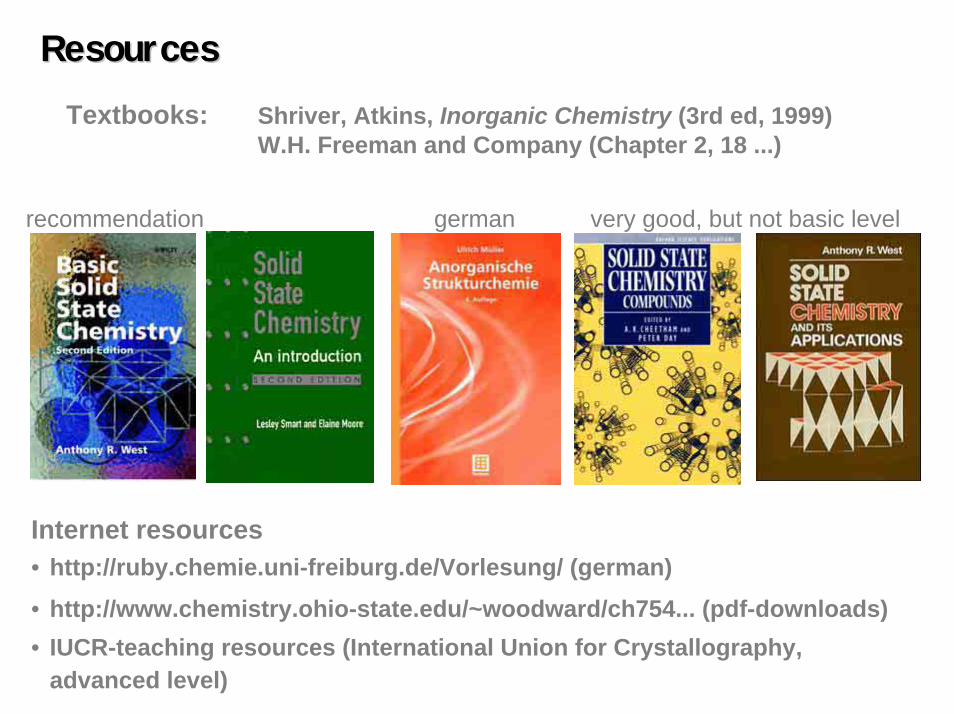
Resources Resources Textbooks: Shriver, Atkins, Inorganic Chemistry (3rd ed, 1999)
W.H. Freeman and Company (Chapter 2, 18 ...)
recommendation german
Internet resources• http://ruby.chemie.uni-freiburg.de/Vorlesung/ (german)
• http://www.chemistry.ohio-state.edu/~woodward/ch754... (pdf-downloads)
• IUCR-teaching resources (International Union for Crystallography, advanced level)
very good, but not basic level

Resources Resources
Journals
Lattice Energy and Chemical Bonding in Solids
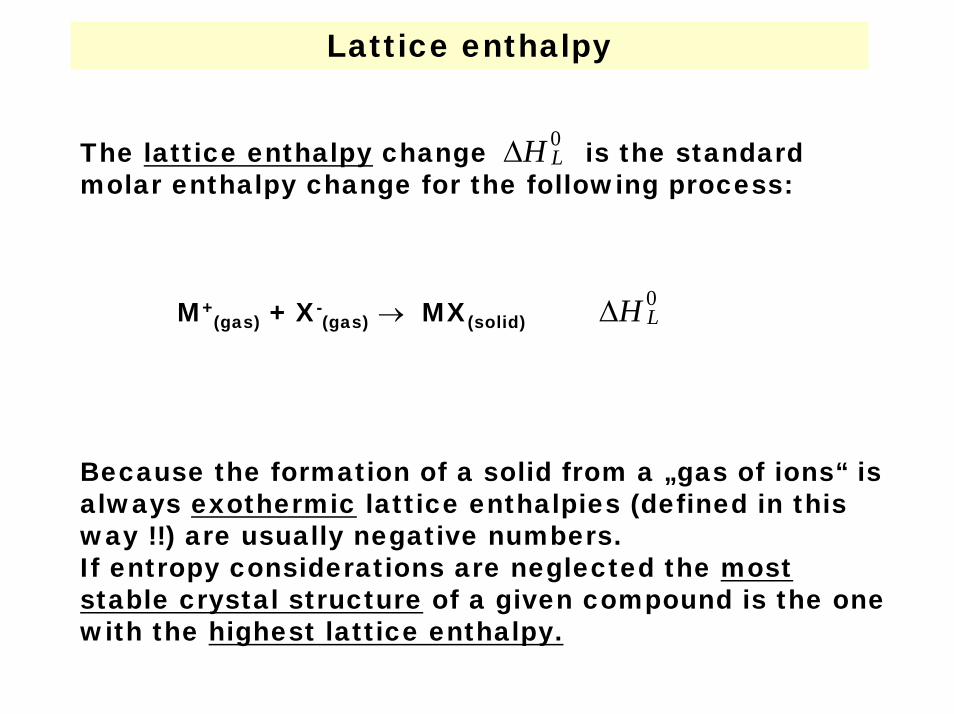
Lattice enthalpy
The lattice enthalpy change is the standardmolar enthalpy change for the following process:
M+(gas) + X-
(gas) → MX(solid)
Because the formation of a solid from a „gas of ions“ isalways exothermic lattice enthalpies (defined in thisway !!) are usually negative numbers.If entropy considerations are neglected the moststable crystal structure of a given compound is the onewith the highest lattice enthalpy.
H L∆ 0
H L∆ 0
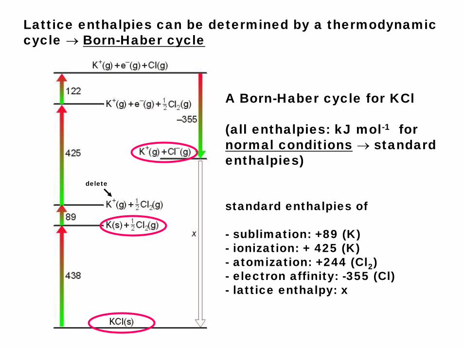
Lattice enthalpies can be determined by a thermodynamiccycle → Born-Haber cycle
A Born-Haber cycle for KCl
(all enthalpies: kJ mol-1 fornormal conditions → standardenthalpies)
standard enthalpies of
- sublimation: +89 (K)- ionization: + 425 (K)- atomization: +244 (Cl2)- electron affinity: -355 (Cl)- lattice enthalpy: x
delete
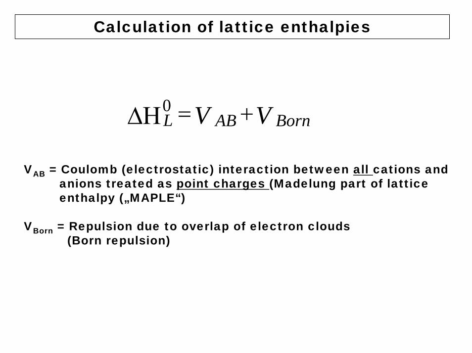
Calculation of lattice enthalpies
VV BornABL +=∆Η0
VAB = Coulomb (electrostatic) interaction between all cations and anions treated as point charges (Madelung part of latticeenthalpy („MAPLE“)
VBorn = Repulsion due to overlap of electron clouds(Born repulsion)
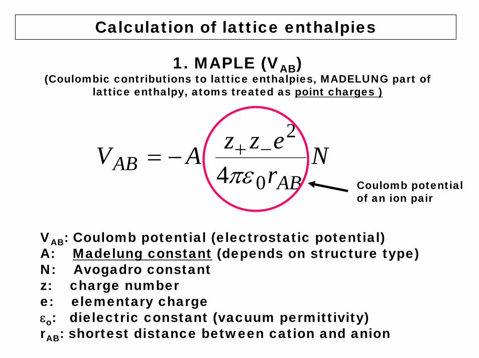
Calculation of lattice enthalpies
1. MAPLE (VAB)(Coulombic contributions to lattice enthalpies, MADELUNG part of
lattice enthalpy, atoms treated as point charges )
NrezzAVAB
AB0
2
4πε−+−=
Coulomb potential of an ion pair
VAB: Coulomb potential (electrostatic potential)A: Madelung constant (depends on structure type)N: Avogadro constantz: charge numbere: elementary chargeεo: dielectric constant (vacuum permittivity)rAB: shortest distance between cation and anion
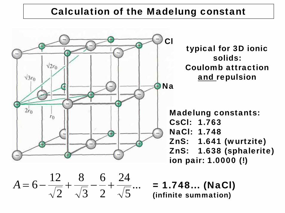
Calculation of the Madelung constant
Na
Cltypical for 3D ionic
solids: Coulomb attraction
and repulsion
Madelung constants:CsCl: 1.763NaCl: 1.748ZnS: 1.641 (wurtzite)ZnS: 1.638 (sphalerite)ion pair: 1.0000 (!)
...5
2426
38
2126 +−+−=A = 1.748... (NaCl)
(infinite summation)
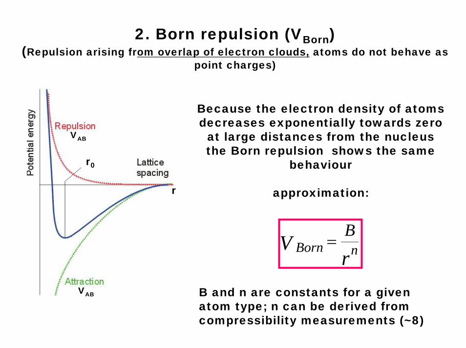
2. Born repulsion (VBorn) (Repulsion arising from overlap of electron clouds, atoms do not behave as
point charges)
Because the electron density of atomsdecreases exponentially towards zero
at large distances from the nucleusthe Born repulsion shows the same
behaviour
approximation:r
r0
VAB
VAB
rV nBorn
B=
B and n are constants for a givenatom type; n can be derived fromcompressibility measurements (~8)
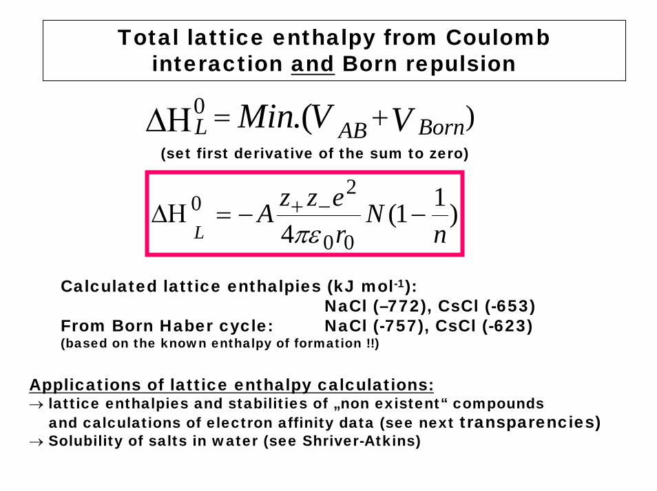
Total lattice enthalpy from Coulombinteraction and Born repulsion
).(0 VVMin BornABL +=∆Η
)11(4 00
20
nN
rezzA
L−−=∆Η −+
πε
(set first derivative of the sum to zero)
Calculated lattice enthalpies (kJ mol-1): NaCl (–772), CsCl (-653)
From Born Haber cycle: NaCl (-757), CsCl (-623) (based on the known enthalpy of formation !!)
Applications of lattice enthalpy calculations:→ lattice enthalpies and stabilities of „non existent“ compounds
and calculations of electron affinity data (see next transparencies)→ Solubility of salts in water (see Shriver-Atkins)
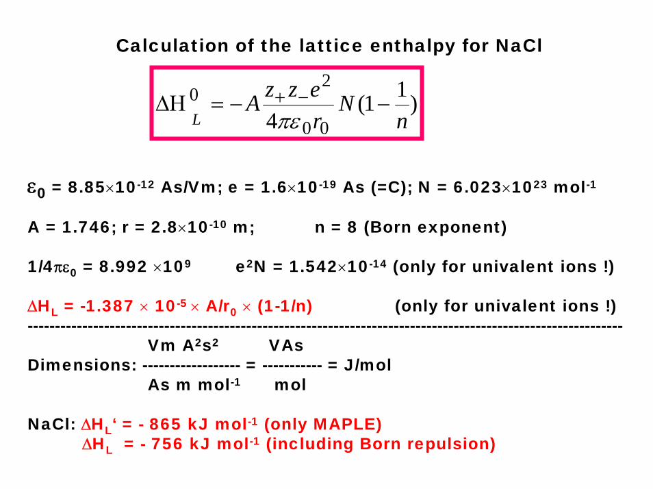
Calculation of the lattice enthalpy for NaCl
)11(4 00
20
nN
rezzA
L−−=∆Η −+
πε
ε0 = 8.85×10⁻¹² As/Vm; e = 1.6×10⁻¹⁹ As (=C); N = 6.023×10²³ mol-1
A = 1.746; r = 2.8×10⁻¹⁰ m; n = 8 (Born exponent)
1/4πε0 = 8.992 ×10⁹ e2N = 1.542×10⁻¹⁴ (only for univalent ions !)
∆HL = -1.387 × 10⁻⁵ × A/r0 × (1-1/n) (only for univalent ions !)-------------------------------------------------------------------------------------------------------------
Vm A2s2 VAsDimensions: ------------------ = ----------- = J/mol
As m mol-1 mol
NaCl: ∆HL‘ = - 865 kJ mol-1 (only MAPLE)∆HL = - 756 kJ mol-1 (including Born repulsion)
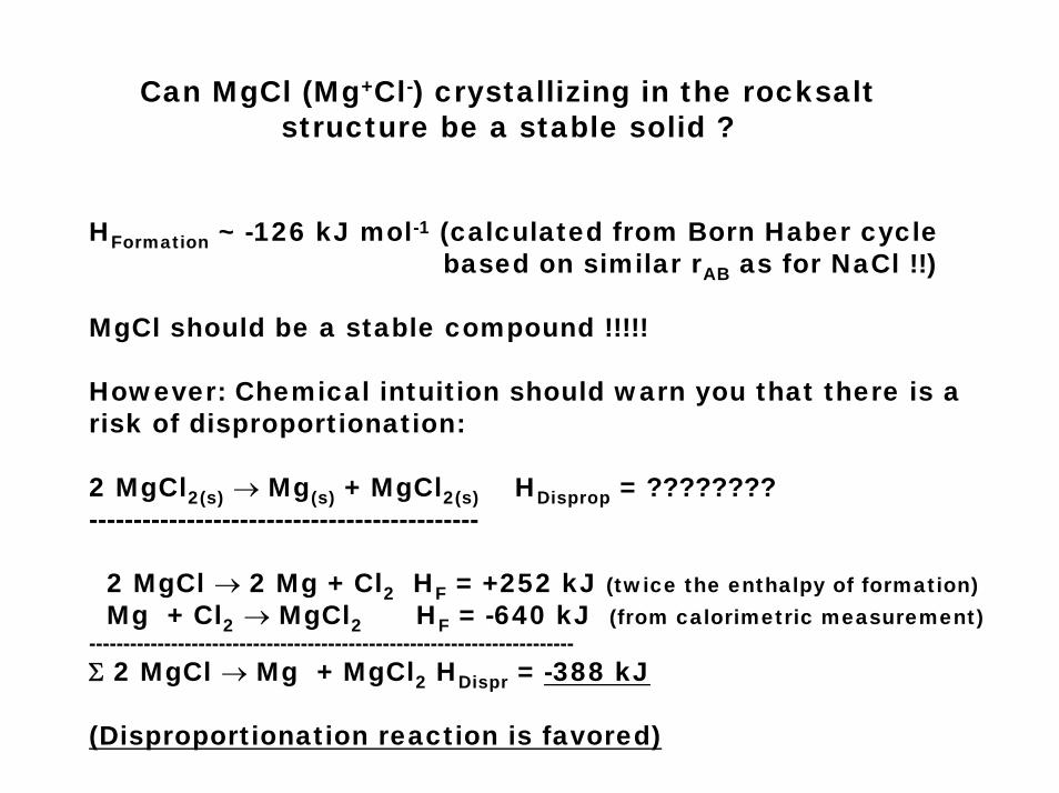
Can MgCl (Mg+Cl-) crystallizing in the rocksaltstructure be a stable solid ?
HFormation ~ -126 kJ mol-1 (calculated from Born Haber cyclebased on similar rAB as for NaCl !!)
MgCl should be a stable compound !!!!!
However: Chemical intuition should warn you that there is a risk of disproportionation:
2 MgCl2(s) → Mg(s) + MgCl2(s) HDisprop = ????????--------------------------------------------
2 MgCl → 2 Mg + Cl2 HF = +252 kJ (twice the enthalpy of formation)Mg + Cl2 → MgCl2 HF = -640 kJ (from calorimetric measurement)
-----------------------------------------------------------------------Σ 2 MgCl → Mg + MgCl2 HDispr = -388 kJ
(Disproportionation reaction is favored)
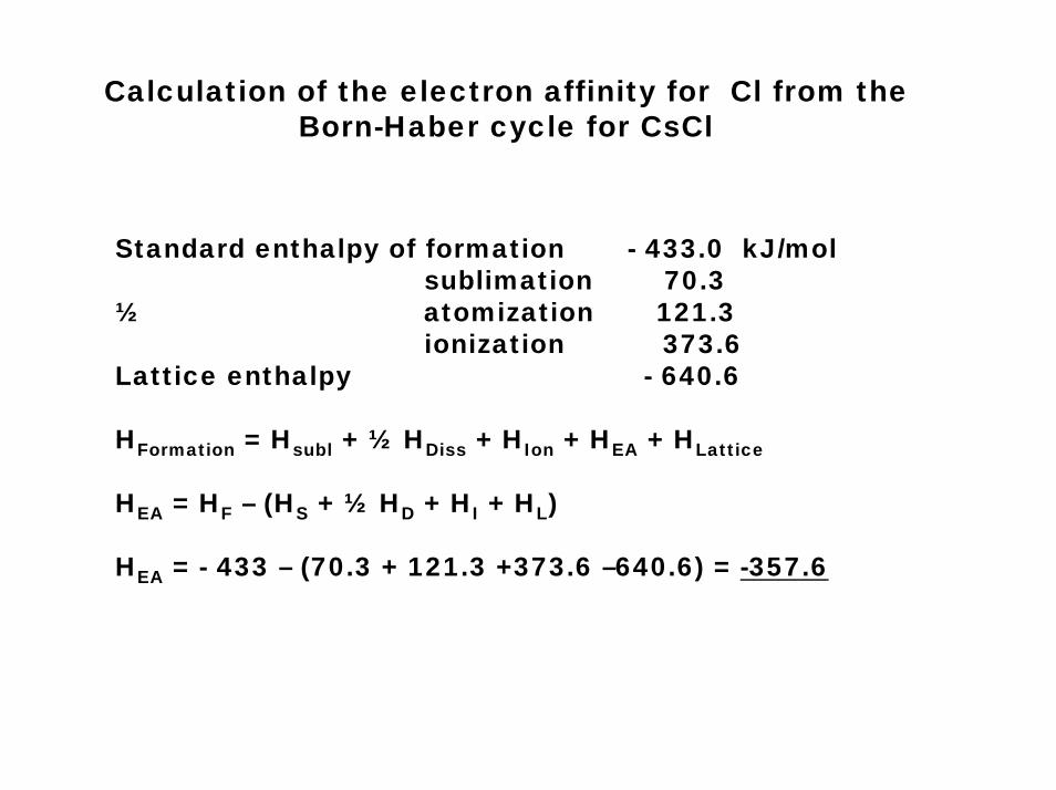
Calculation of the electron affinity for Cl from theBorn-Haber cycle for CsCl
Standard enthalpy of formation - 433.0 kJ/molsublimation 70.3
½ atomization 121.3ionization 373.6
Lattice enthalpy - 640.6
HFormation = Hsubl + ½ HDiss + HIon + HEA + HLattice
HEA = HF – (HS + ½ HD + HI + HL)
HEA = - 433 – (70.3 + 121.3 +373.6 –640.6) = -357.6
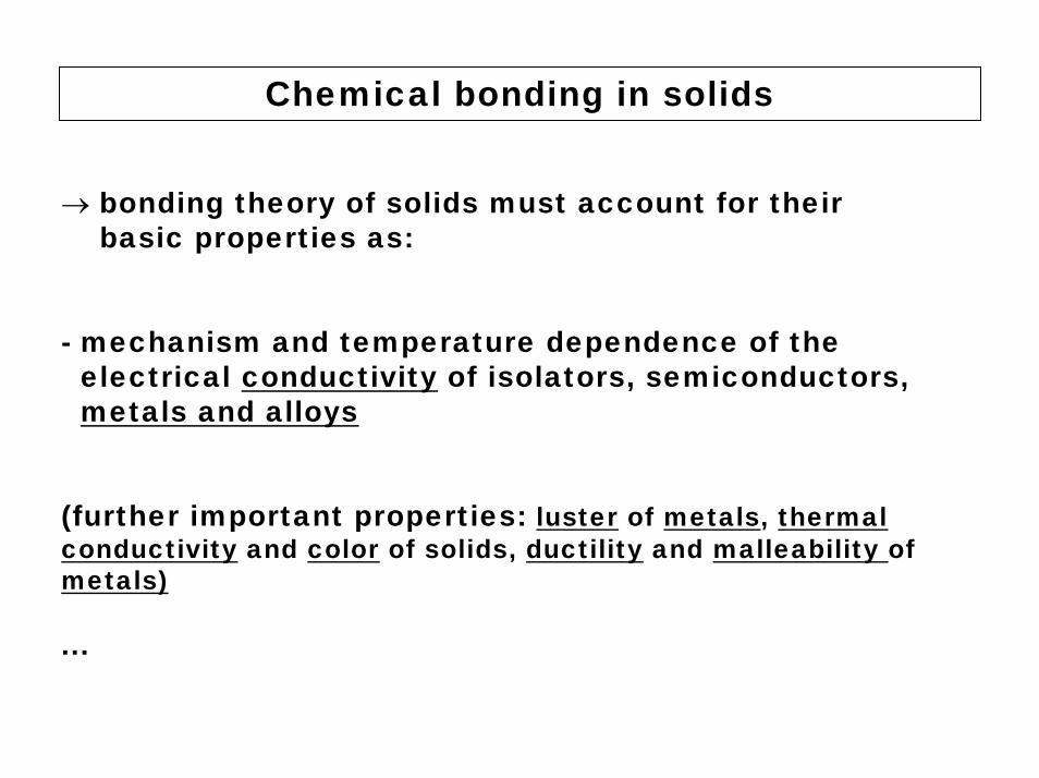
Chemical bonding in solids
→ bonding theory of solids must account for theirbasic properties as:
- mechanism and temperature dependence of theelectrical conductivity of isolators, semiconductors,metals and alloys
(further important properties: luster of metals, thermal conductivity and color of solids, ductility and malleability of metals)
...
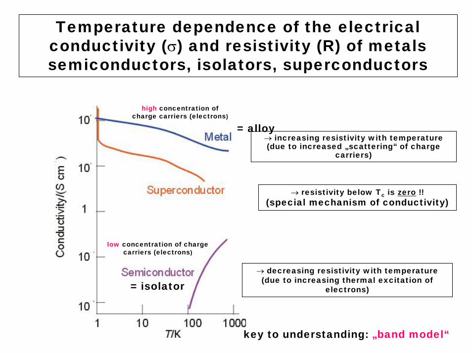
Temperature dependence of the electricalconductivity (σ) and resistivity (R) of metals semiconductors, isolators, superconductors
= isolator
= alloy→ increasing resistivity with temperature(due to increased „scattering“ of charge
carriers)
→ resistivity below Tc is zero !!(special mechanism of conductivity)
→ decreasing resistivity with temperature(due to increasing thermal excitation of
electrons)
key to understanding: „band model“
high concentration of charge carriers (electrons)
low concentration of chargecarriers (electrons)
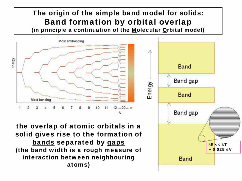
The origin of the simple band model for solids:Band formation by orbital overlap
(in principle a continuation of the Molecular Orbital model)
the overlap of atomic orbitals in a solid gives rise to the formation of
bands separated by gaps(the band width is a rough measure of
interaction between neighbouringatoms)
δE << kT~ 0.025 eV
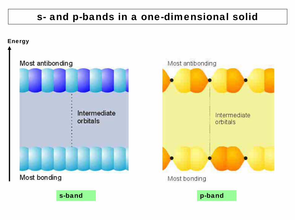
s- and p-bands in a one-dimensional solid
Energy
s-band p-band
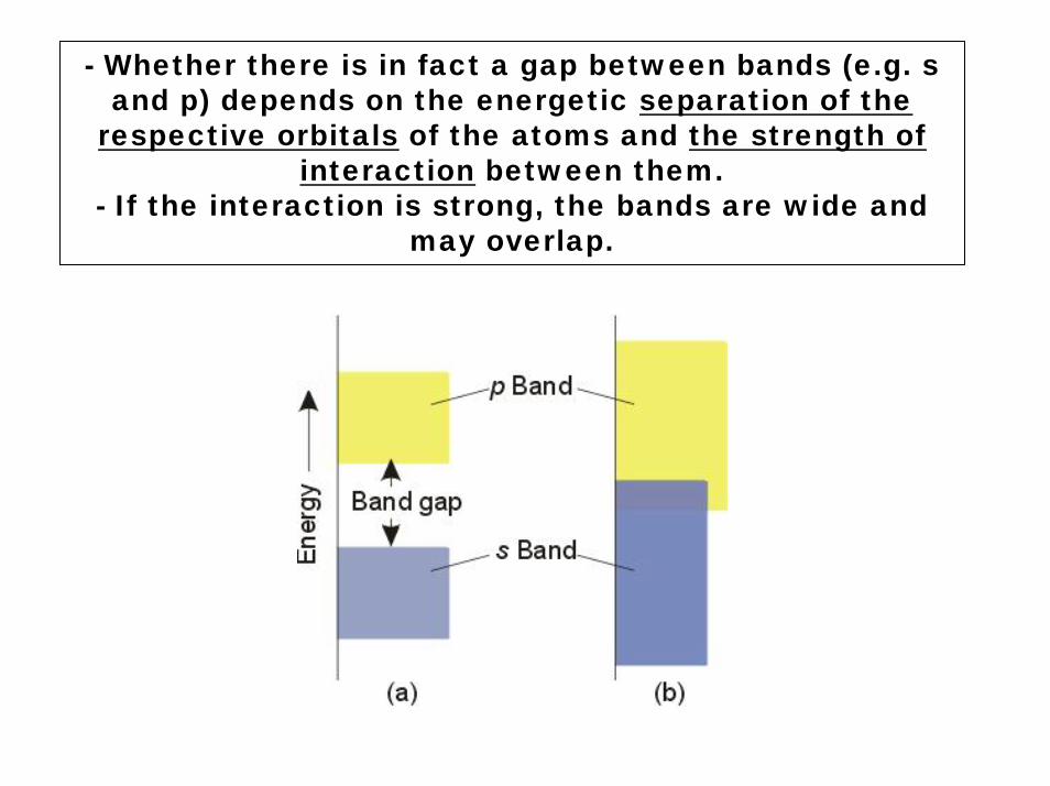
- Whether there is in fact a gap between bands (e.g. s and p) depends on the energetic separation of the
respective orbitals of the atoms and the strength of interaction between them.
- If the interaction is strong, the bands are wide and may overlap.
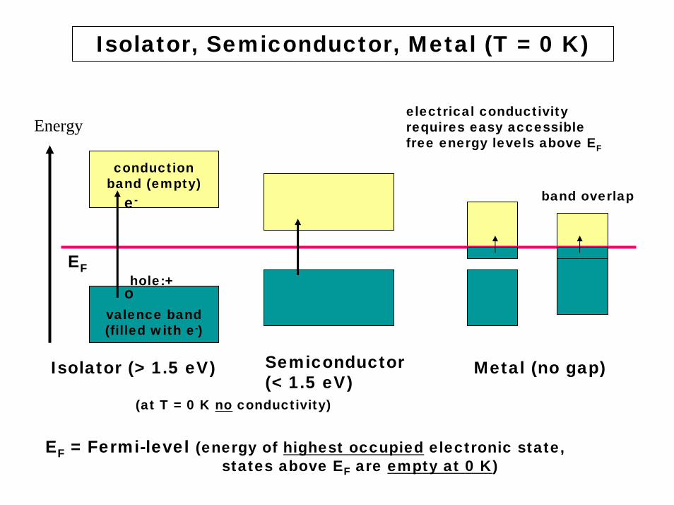
Isolator, Semiconductor, Metal (T = 0 K)
electrical conductivityrequires easy accessiblefree energy levels above EF
Energy
EF
valence band(filled with e-)
conductionband (empty)
band overlap
o
e-
hole:+
Semiconductor(< 1.5 eV)
Isolator (> 1.5 eV) Metal (no gap)
(at T = 0 K no conductivity)
EF = Fermi-level (energy of highest occupied electronic state, states above EF are empty at 0 K)
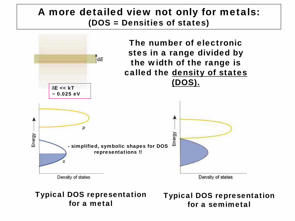
A more detailed view not only for metals:(DOS = Densities of states)
The number of electronicstes in a range divided bythe width of the range is
called the density of states(DOS).
δE << kT~ 0.025 eV
- simplified, symbolic shapes for DOS representations !!
Typical DOS representationfor a metal
Typical DOS representationfor a semimetal
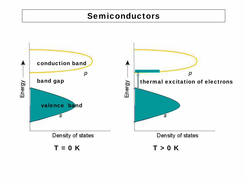
Semiconductors
conduction band
valence band
band gap thermal excitation of electrons
T = 0 K T > 0 K

Temperature dependence of the electricalconductivity (σ) and resistivity (R) of metals semiconductors, isolators, superconductors
= isolator
= alloy→ increasing resistivity with temperature(due to increased „scattering“ of charge
carriers)
→ resistivity below Tc is zero !!(special mechanism of conductivity)
→ decreasing resistivity with temperature(due to increasing thermal excitation of
electrons)
key to understanding: „band model“
high concentration of charge carriers (electrons)
low concentration of chargecarriers (electrons)
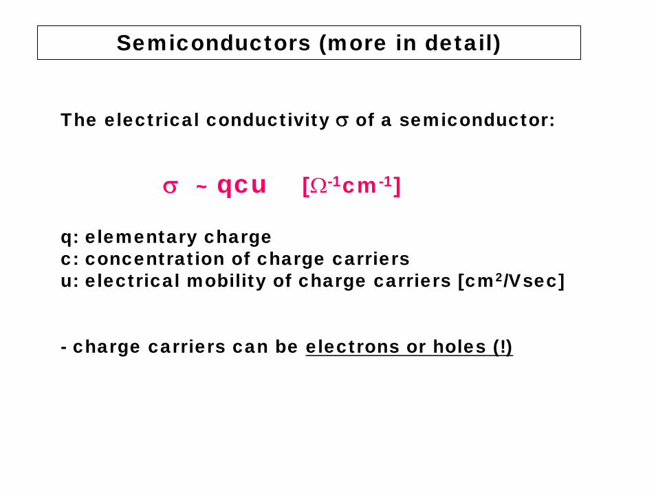
Semiconductors (more in detail)
The electrical conductivity σ of a semiconductor:
σ ~ qcu [Ω-1cm-1]
q: elementary chargec: concentration of charge carriersu: electrical mobility of charge carriers [cm2/Vsec]
- charge carriers can be electrons or holes (!)
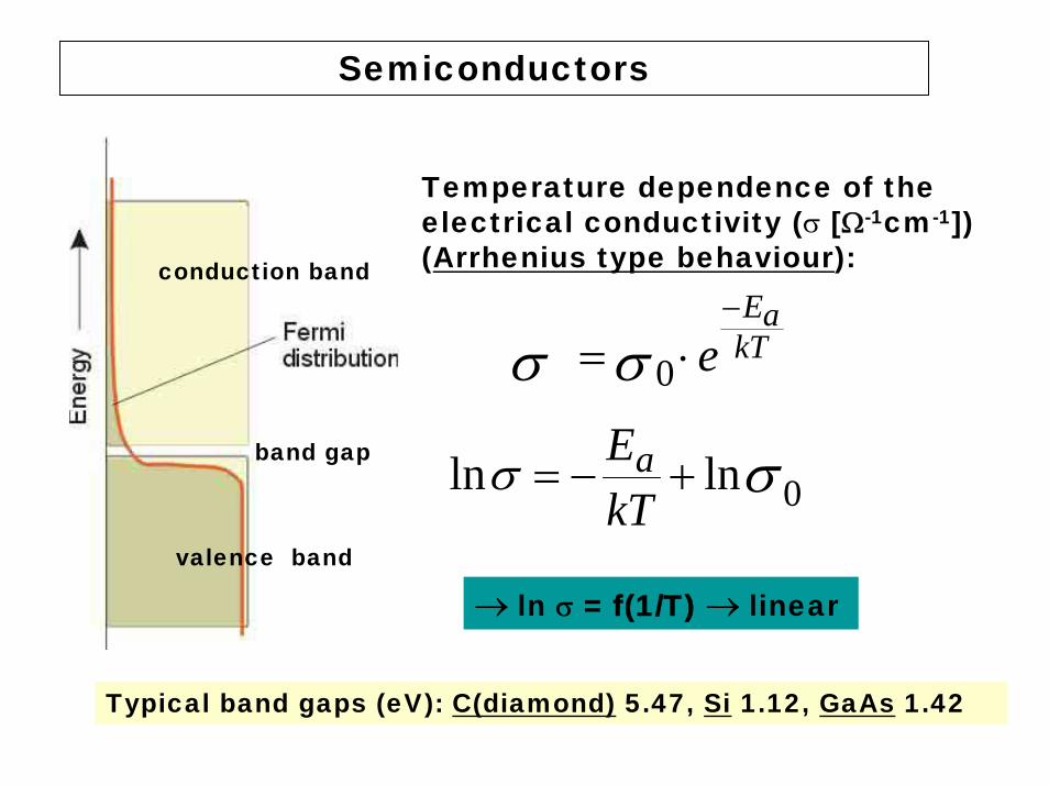
Semiconductors
conduction band
band gap
valence band
Temperature dependence of theelectrical conductivity (σ [Ω-1cm-1])(Arrhenius type behaviour):
kTaE
e−
⋅=σσ 0
0lnln σσ +−=kTEa
→ ln σ = f(1/T) → linear
Typical band gaps (eV): C(diamond) 5.47, Si 1.12, GaAs 1.42
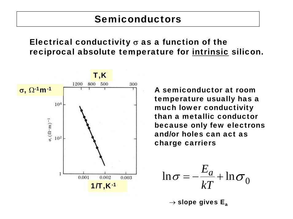
Semiconductors
Electrical conductivity σ as a function of thereciprocal absolute temperature for intrinsic silicon.
σ, Ω-1m-1
T,K
1/T,K-1
A semiconductor at roomtemperature usually has a much lower conductivitythan a metallic conductorbecause only few electronsand/or holes can act as charge carriers
0lnln σσ +−=kTEa
→ slope gives Ea
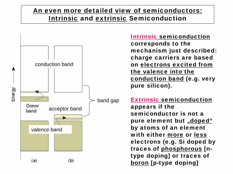
An even more detailed view of semiconductors:Intrinsic and extrinsic Semiconduction
Intrinsic semiconductioncorresponds to themechanism just described: charge carriers are basedon electrons excited fromthe valence into theconduction band (e.g. verypure silicon).
Extrinsic semiconductionappears if thesemiconductor is not a pure element but „doped“by atoms of an elementwith either more or lesselectrons (e.g. Si doped bytraces of phosphorous [n-type doping] or traces of boron [p-type doping]
acceptor band
conduction band
valence band
band gap
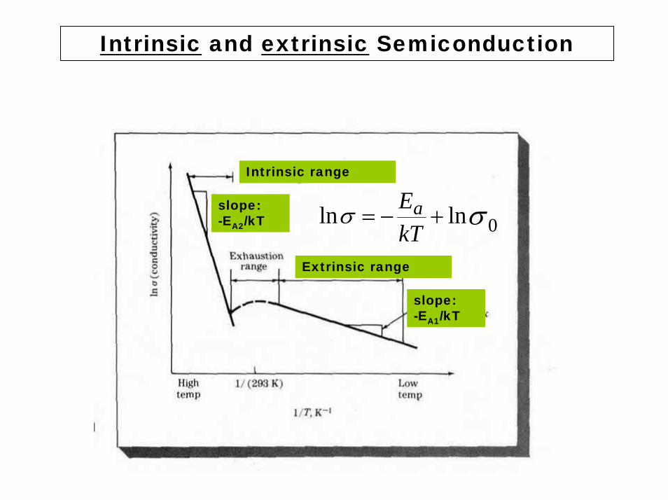
Intrinsic and extrinsic Semiconduction
0lnln σσ +−=kTEa
slope:-EA1/kT
slope:-EA2/kT
Extrinsic range
Intrinsic range
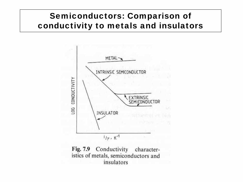
Semiconductors: Comparison of conductivity to metals and insulators
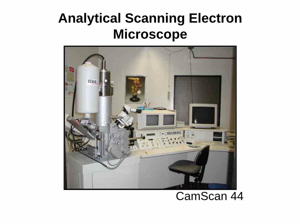
Analytical Scanning ElectronMicroscope
CamScan 44
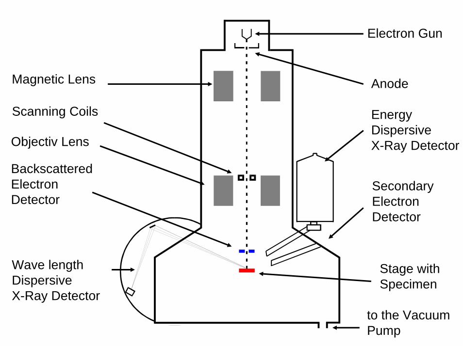
Electron Gun
Magnetic Lens Anode
Scanning Coils EnergyDispersiveX-Ray DetectorObjectiv Lens
Wave lengthDispersiveX-Ray Detector
to the VacuumPump
BackscatteredElectronDetector
SecondaryElectronDetector
Stage withSpecimen

Electron Gun (W-Cathode)
Wehnelt Cylinder(500 V more negativethan the Cathode,„Bias“)
Crossover (20-50 µm)Electron beam source
20000 V
HeatingCurrent (DC)
Cathode
Tungsten
Anodegrounding
The crossover is belittlet projected on the sampleby the electronic-optical system(minimal diameter of the beam: ca. 5 nm)
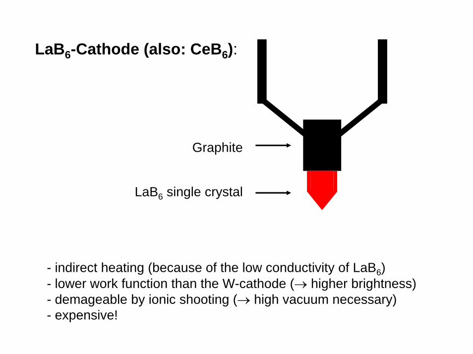
LaB6-Cathode (also: CeB6):
LaB6 single crystal
Graphite
- indirect heating (because of the low conductivity of LaB6)- lower work function than the W-cathode (→ higher brightness)- demageable by ionic shooting (→ high vacuum necessary)- expensive!
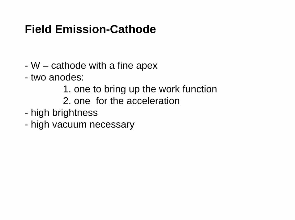
Field Emission-Cathode
- W – cathode with a fine apex- two anodes:
1. one to bring up the work function2. one for the acceleration
- high brightness- high vacuum necessary
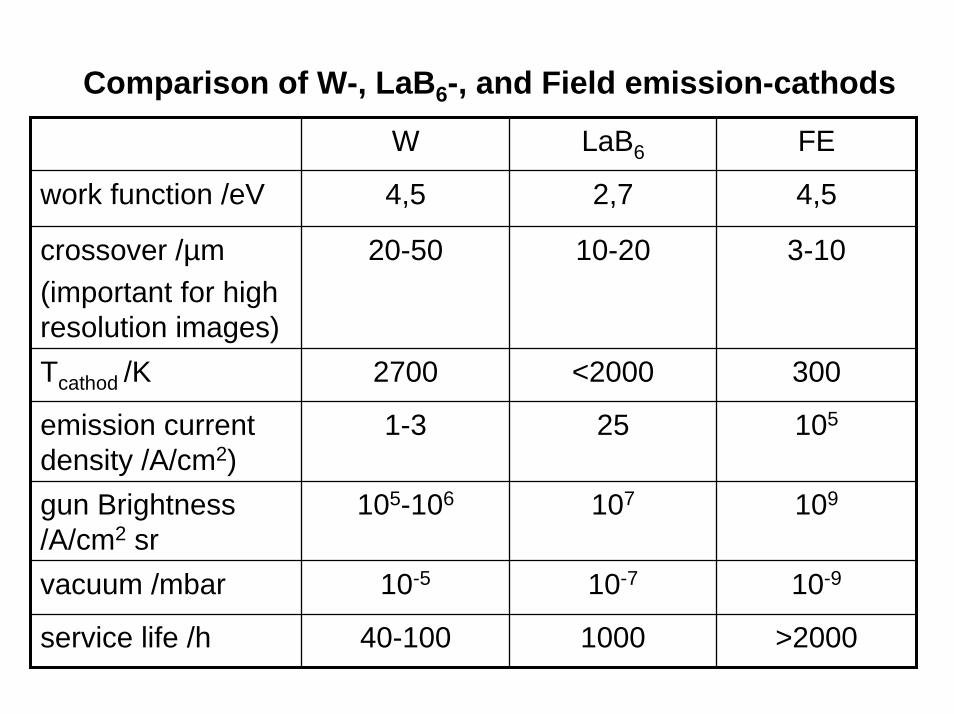
Comparison of W-, LaB6-, and Field emission-cathods
W LaB6 FE
work function /eV 4,5 2,7 4,5
crossover /µm
(important for high resolution images)
20-50 10-20 3-10
Tcathod /K 2700 <2000 300
emission currentdensity /A/cm2)
1-3 25 105
gun Brightness/A/cm2 sr
105-106 107 109
vacuum /mbar 10-5 10-7 10-9
service life /h 40-100 1000 >2000
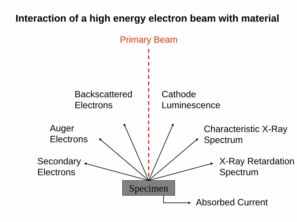
Interaction of a high energy electron beam with material
Primary Beam
Specimen
BackscatteredElectrons
CathodeLuminescence
AugerElectrons
Characteristic X-RaySpectrum
X-Ray RetardationSpectrum
SecondaryElectrons
Absorbed Current
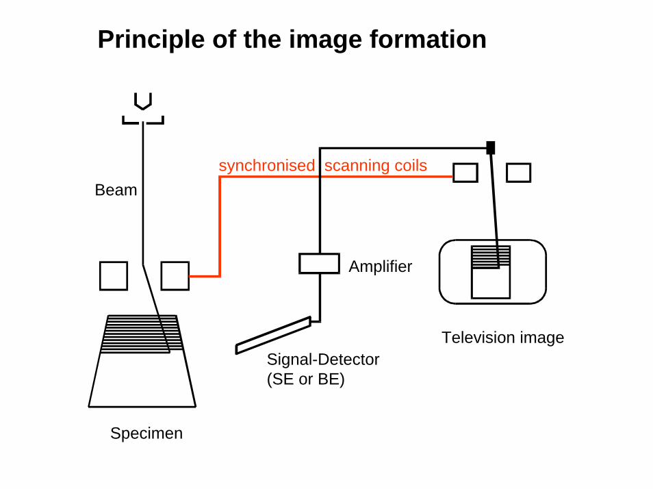
Principle of the image formation
Signal-Detector(SE or BE)
synchronised scanning coils
Television image
Amplifier
Beam
Specimen
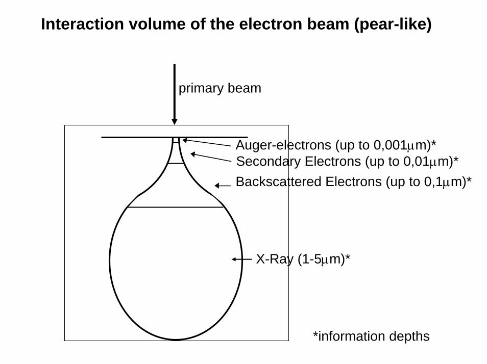
Interaction volume of the electron beam (pear-like)
Auger-electrons (up to 0,001µm)*Secondary Electrons (up to 0,01µm)*
Backscattered Electrons (up to 0,1µm)*
X-Ray (1-5µm)*
primary beam
*information depths
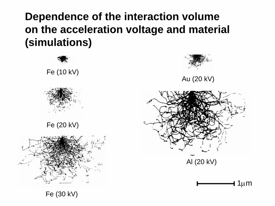
Dependence of the interaction volumeon the acceleration voltage and material(simulations)
Fe (10 kV)Au (20 kV)
Fe (20 kV)
Al (20 kV)
1µm
Fe (30 kV)
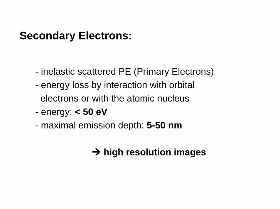
Secondary Electrons:
- inelastic scattered PE (Primary Electrons)
- energy loss by interaction with orbital
electrons or with the atomic nucleus
- energy: < 50 eV
- maximal emission depth: 5-50 nm
high resolution images
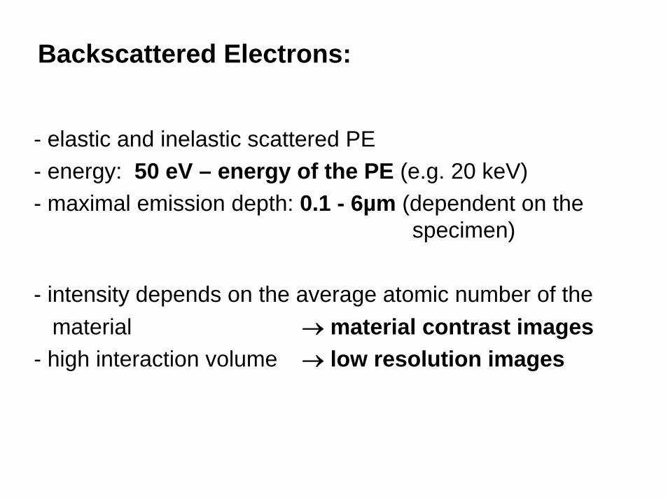
Backscattered Electrons:
- elastic and inelastic scattered PE
- energy: 50 eV – energy of the PE (e.g. 20 keV)
- maximal emission depth: 0.1 - 6µm (dependent on thespecimen)
- intensity depends on the average atomic number of the
material → material contrast images
- high interaction volume → low resolution images
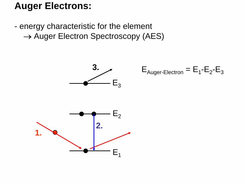
Auger Electrons:
- energy characteristic for the element→ Auger Electron Spectroscopy (AES)
3.
E3
EAuger-Electron = E1-E2-E3
1.
E1
E2
2.
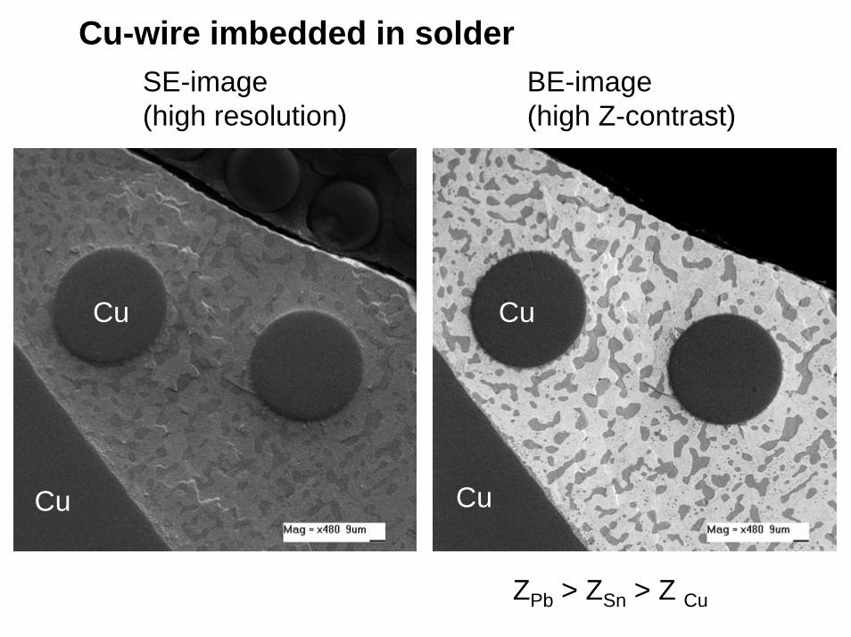
Cu-wire imbedded in solder
SE-image(high resolution)
BE-image(high Z-contrast)
Cu Cu
Cu Cu
ZPb > ZSn > Z Cu
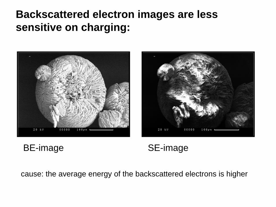
Backscattered electron images are lesssensitive on charging:
BE-image SE-image
cause: the average energy of the backscattered electrons is higher
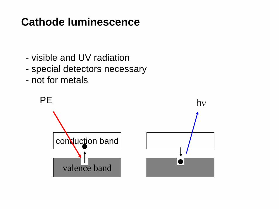
Cathode luminescence
- visible and UV radiation- special detectors necessary - not for metals
PE
valence band
conduction band
hν
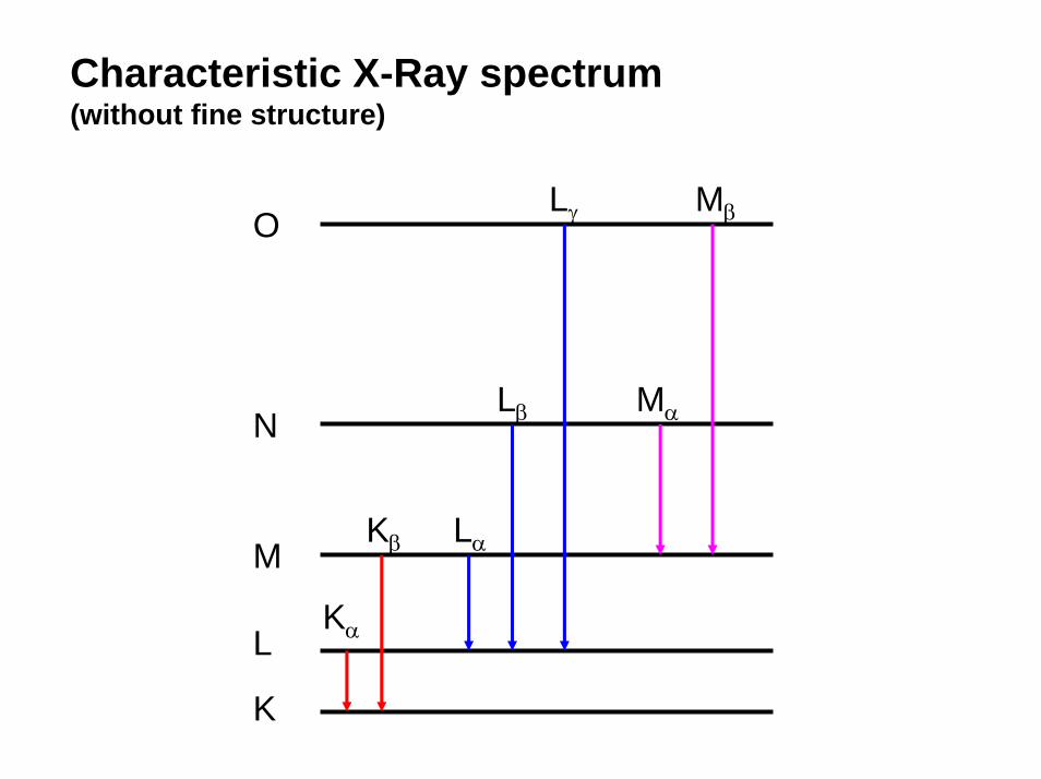
Characteristic X-Ray spectrum(without fine structure)
K
L
N
M
O
Kα
Kβ Lα
Lβ
Lγ
Mα
Mβ
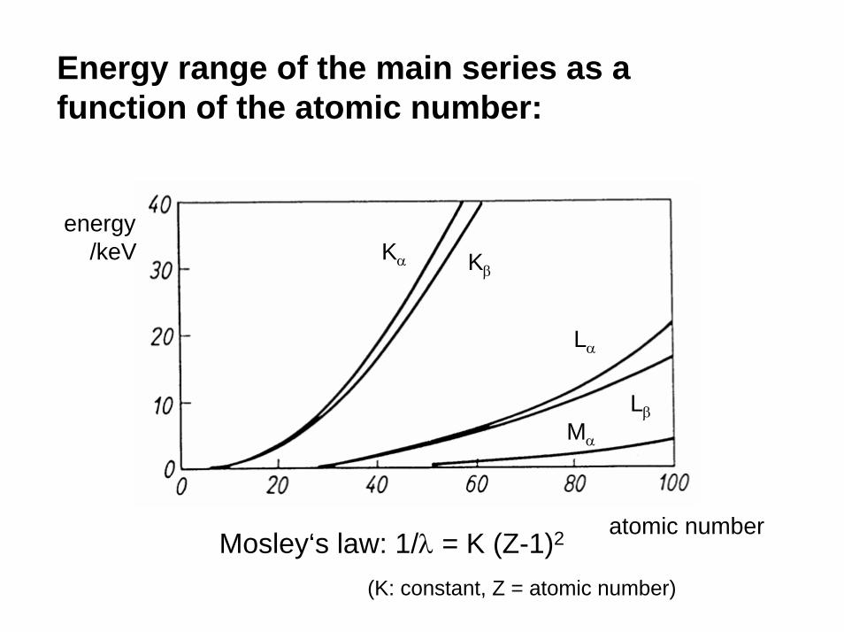
Energy range of the main series as a function of the atomic number:
energy/keV Kα Kβ
Lα
LβMα
atomic numberMosley‘s law: 1/λ = K (Z-1)2
(K: constant, Z = atomic number)
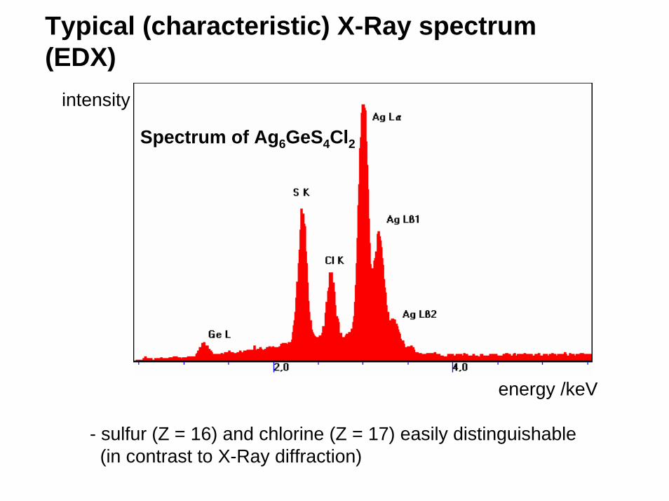
Typical (characteristic) X-Ray spectrum(EDX)
energy /keV
intensity
Spectrum of Ag6GeS4Cl2
- sulfur (Z = 16) and chlorine (Z = 17) easily distinguishable(in contrast to X-Ray diffraction)
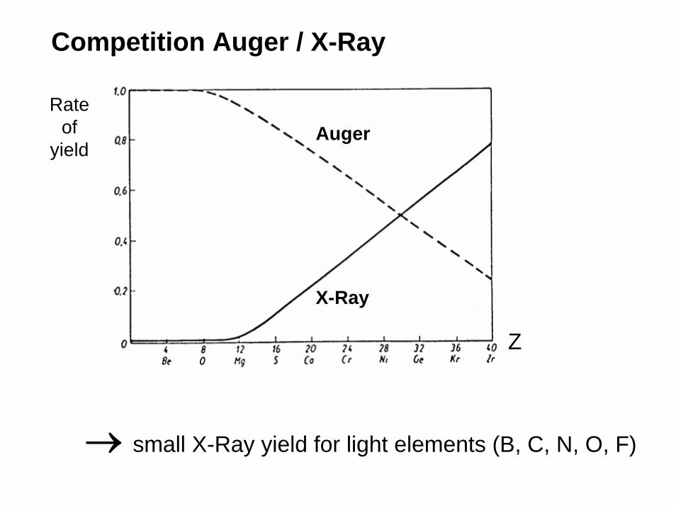
Competition Auger / X-Ray
Auger
X-Ray
Z
Rateof
yield
→ small X-Ray yield for light elements (B, C, N, O, F)
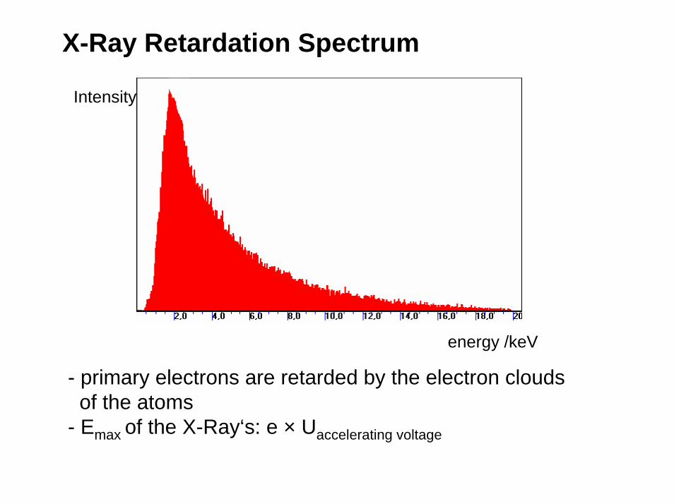
X-Ray Retardation Spectrum
Intensity
energy /keV
- primary electrons are retarded by the electron cloudsof the atoms
- Emax of the X-Ray‘s: e × Uaccelerating voltage
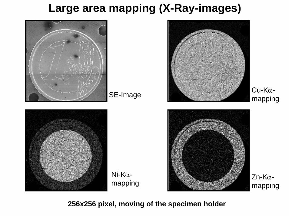
Large area mapping (X-Ray-images)
Cu-Kα-mappingSE-Image
Ni-Kα-mapping
Zn-Kα-mapping
256x256 pixel, moving of the specimen holder
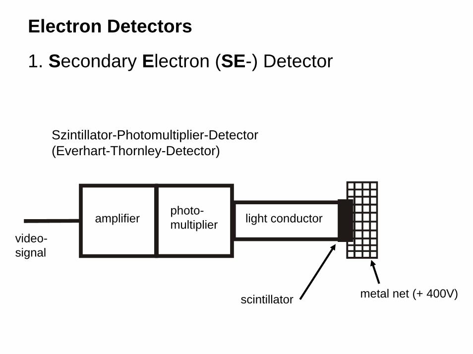
Electron Detectors
1. Secondary Electron (SE-) Detector
Szintillator-Photomultiplier-Detector(Everhart-Thornley-Detector)
video-signal
photo-multiplier light conductor
scintillator metal net (+ 400V)
amplifier
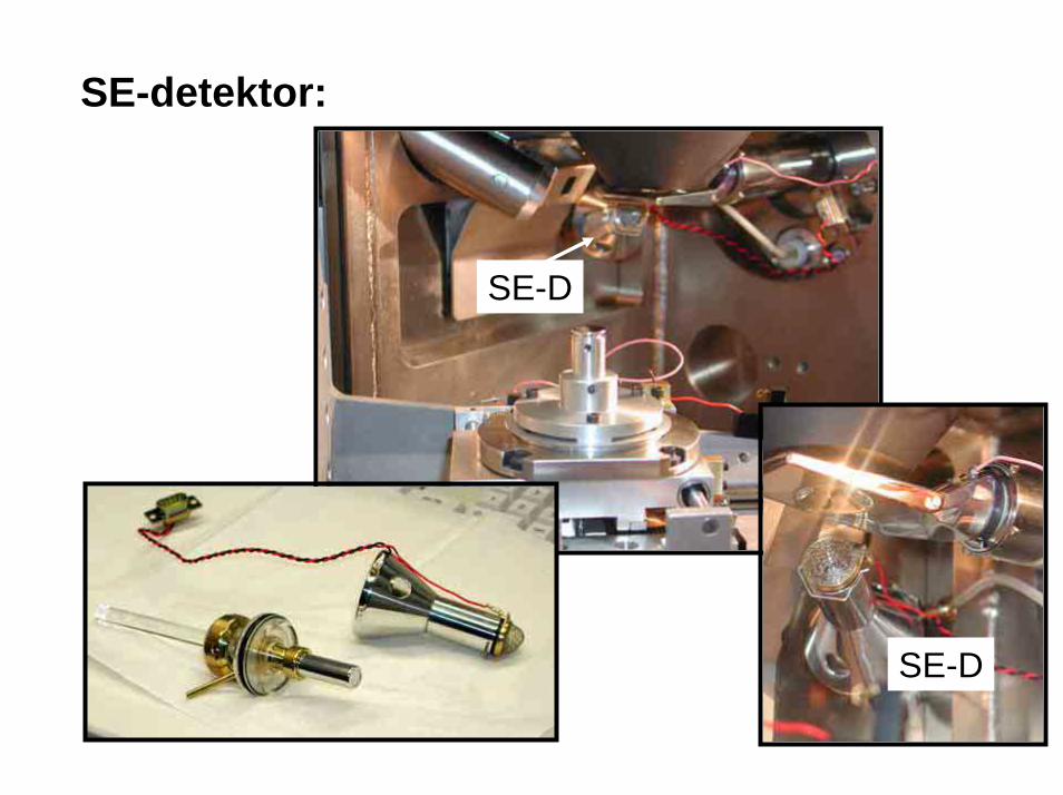
SE-detektor:
SE-D
SE-D
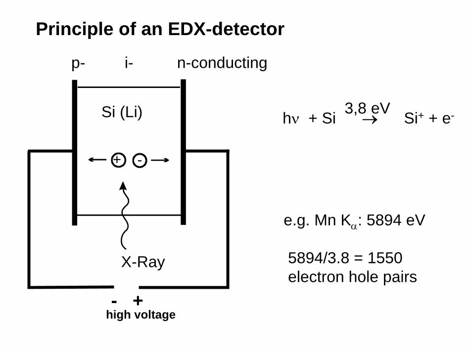
Principle of an EDX-detector
p- i- n-conducting
+ -
X-Ray
Si (Li) hν + Si → Si+ + e-3,8 eV
- +high voltage
e.g. Mn Kα: 5894 eV
5894/3.8 = 1550 electron hole pairs
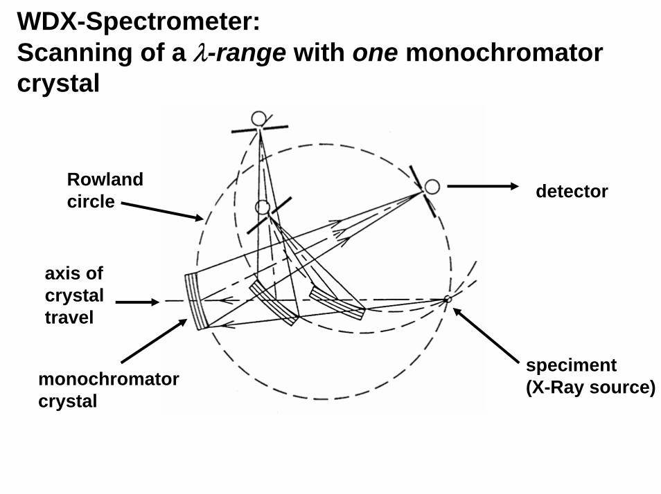
WDX-Spectrometer:Scanning of a λ-range with one monochromatorcrystal
speciment(X-Ray source)monochromator
crystal
detectorRowlandcircle
axis ofcrystaltravel
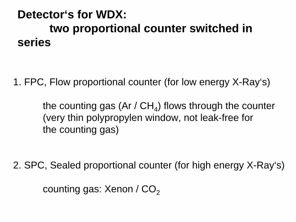
Detector‘s for WDX: two proportional counter switched in
series
1. FPC, Flow proportional counter (for low energy X-Ray‘s)
the counting gas (Ar / CH4) flows through the counter(very thin polypropylen window, not leak-free forthe counting gas)
2. SPC, Sealed proportional counter (for high energy X-Ray‘s)
counting gas: Xenon / CO2
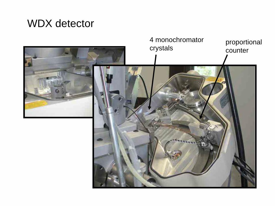
WDX detector
4 monochromatorcrystals
proportionalcounter
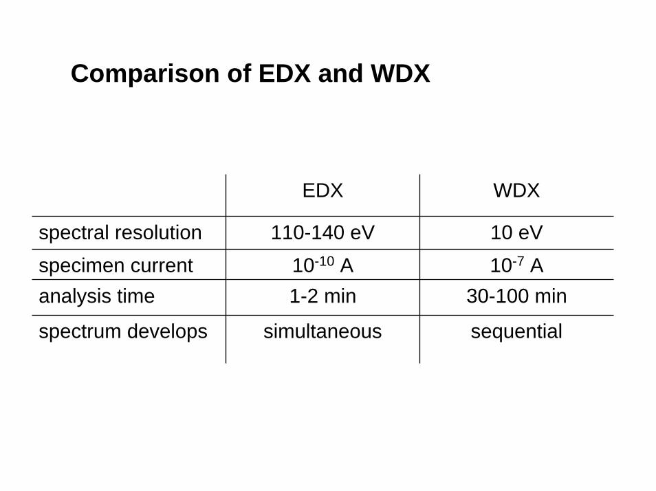
Comparison of EDX and WDX
EDX WDX
spectral resolution 110-140 eV 10 eV
specimen current 10-10 A 10-7 A
analysis time 1-2 min 30-100 min
spectrum develops simultaneous sequential
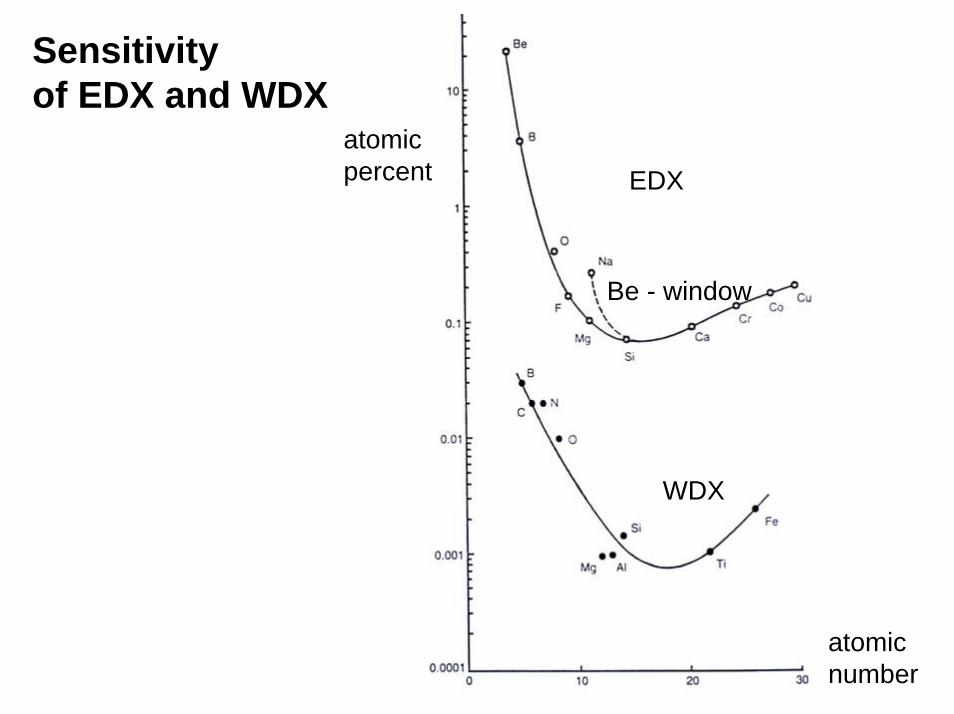
atomicnumber
atomicpercent EDX
WDX
Be - window
Sensitivityof EDX and WDX
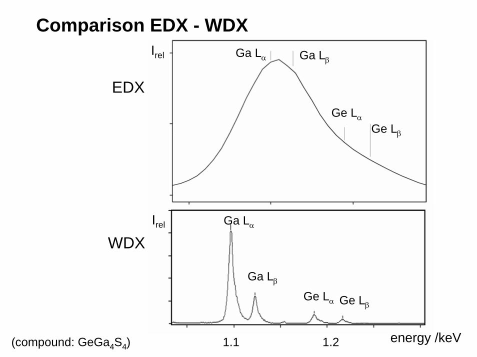
Comparison EDX - WDX
Ga Lα
Ge Lα
Ga Lα
Ge Lα
Ga Lβ
Ge Lβ
Ge Lβ
Ga Lβ
Irel
Irel
energy /keV
EDX
1.1 1.2
WDX
(compound: GeGa4S4)
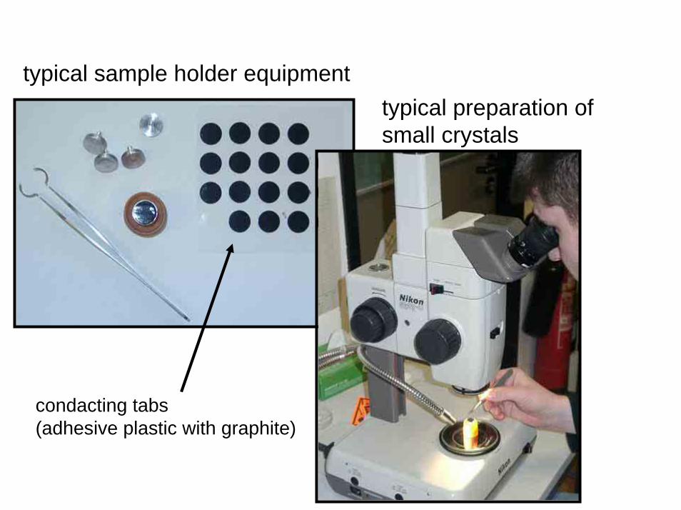
typical sample holder equipment
typical preparation of small crystals
condacting tabs(adhesive plastic with graphite)
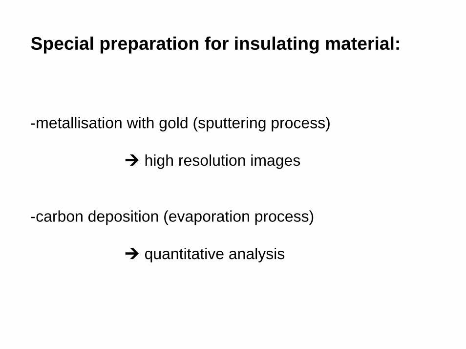
Special preparation for insulating material:
-metallisation with gold (sputtering process)
high resolution images
-carbon deposition (evaporation process)
quantitative analysis
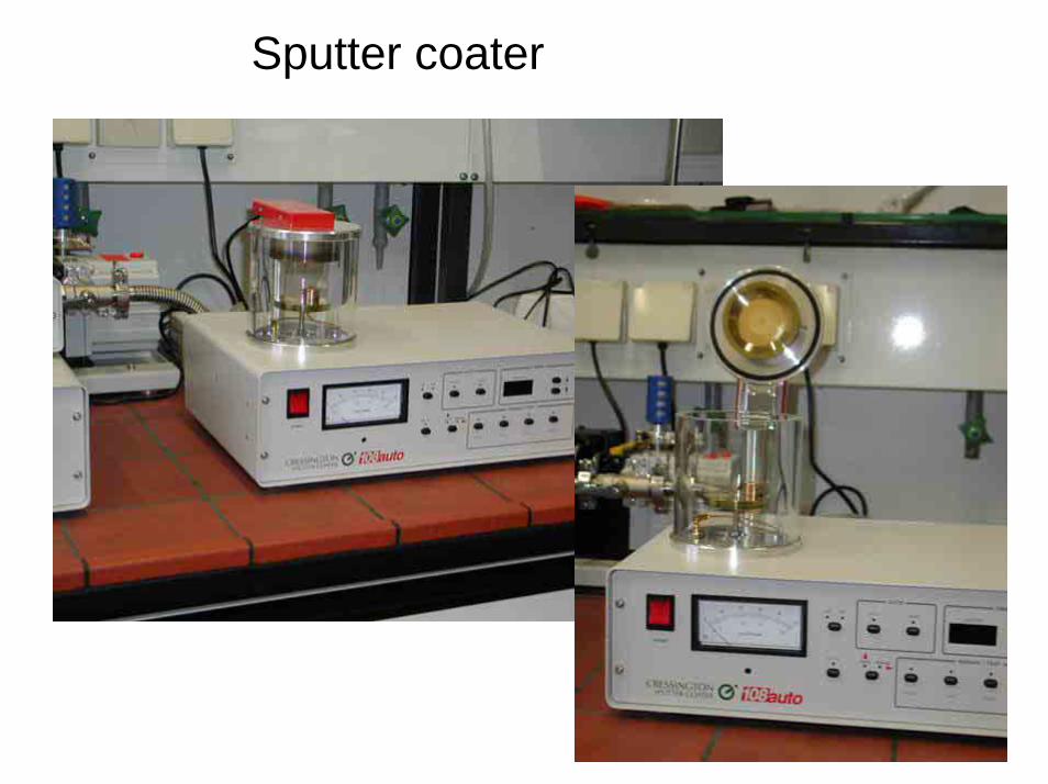
Sputter coater
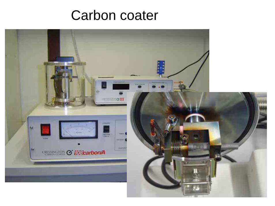
Carbon coater
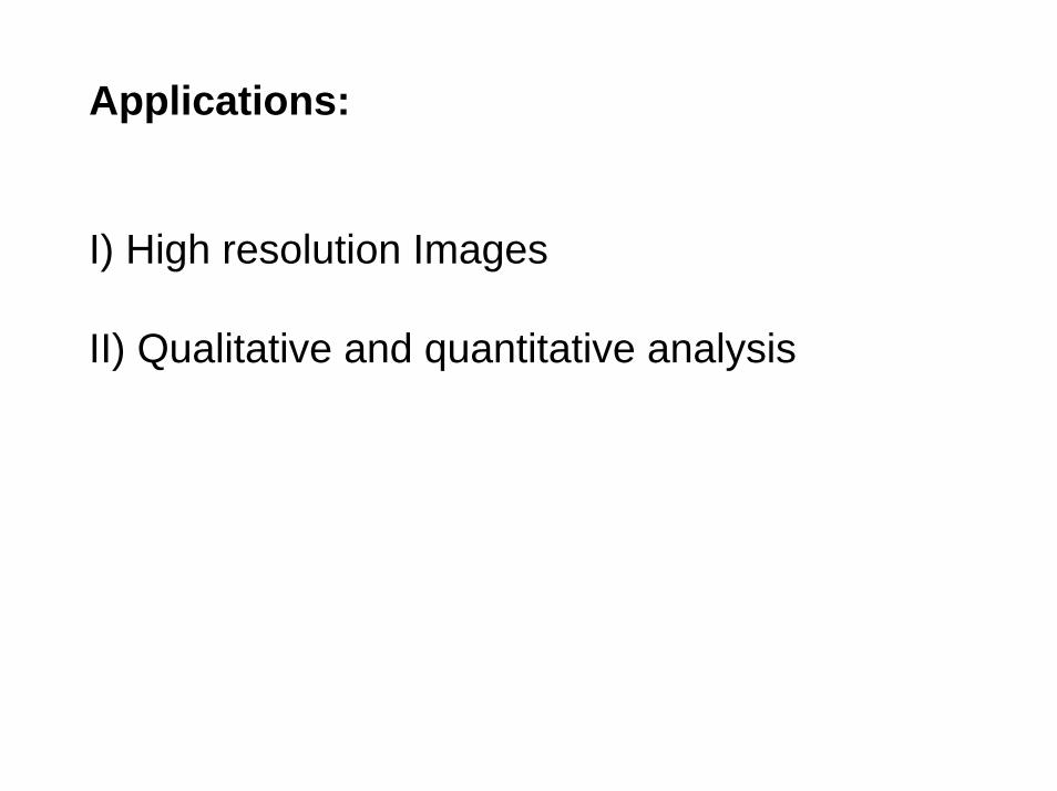
Applications:
I) High resolution Images
II) Qualitative and quantitative analysis
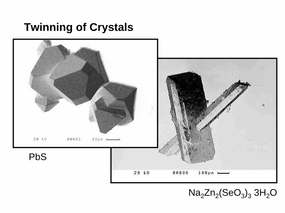
Twinning of Crystals
PbS
Na2Zn2(SeO3)3 3H2O
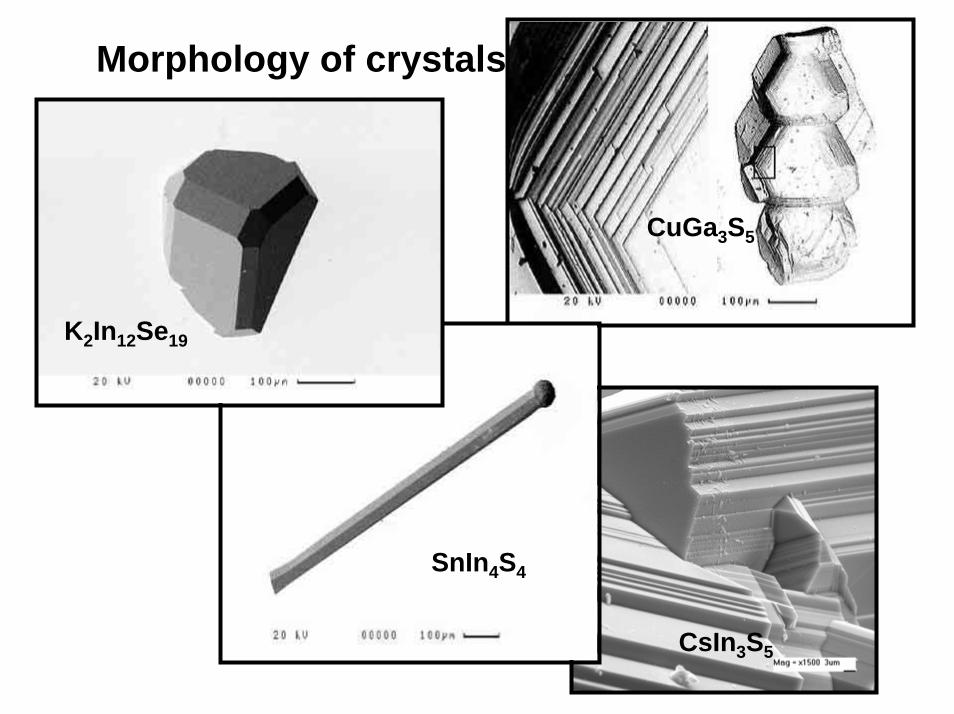
Morphology of crystals
K2In12Se19
SnIn4S4
CsIn3S5
CuGa3S5
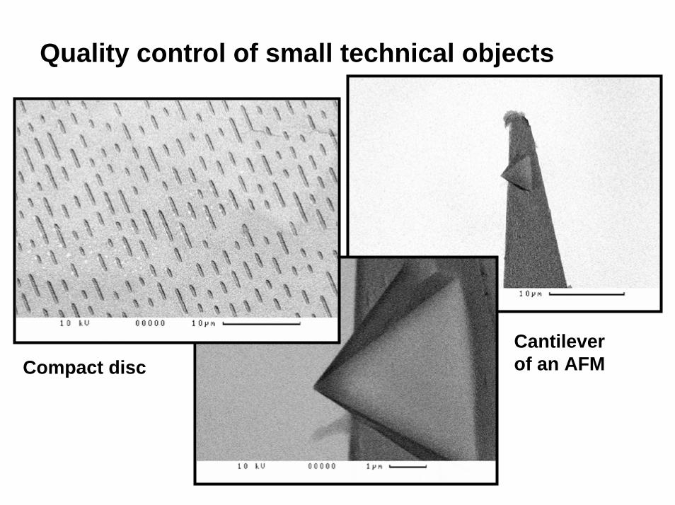
Quality control of small technical objects
Cantileverof an AFMCompact disc
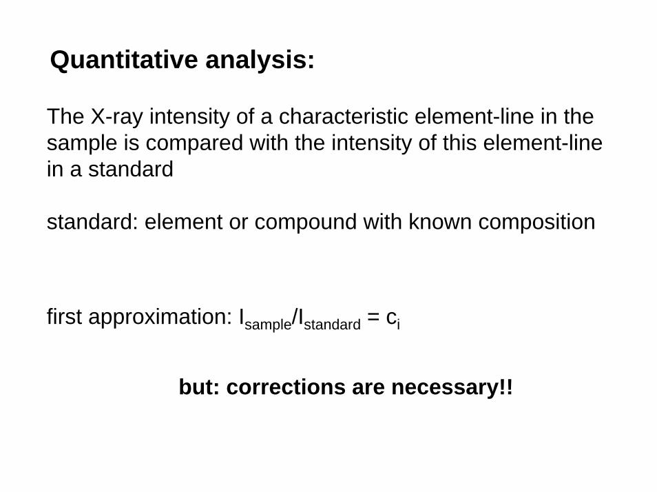
Quantitative analysis:
The X-ray intensity of a characteristic element-line in thesample is compared with the intensity of this element-linein a standard
standard: element or compound with known composition
first approximation: Isample/Istandard = ci
but: corrections are necessary!!
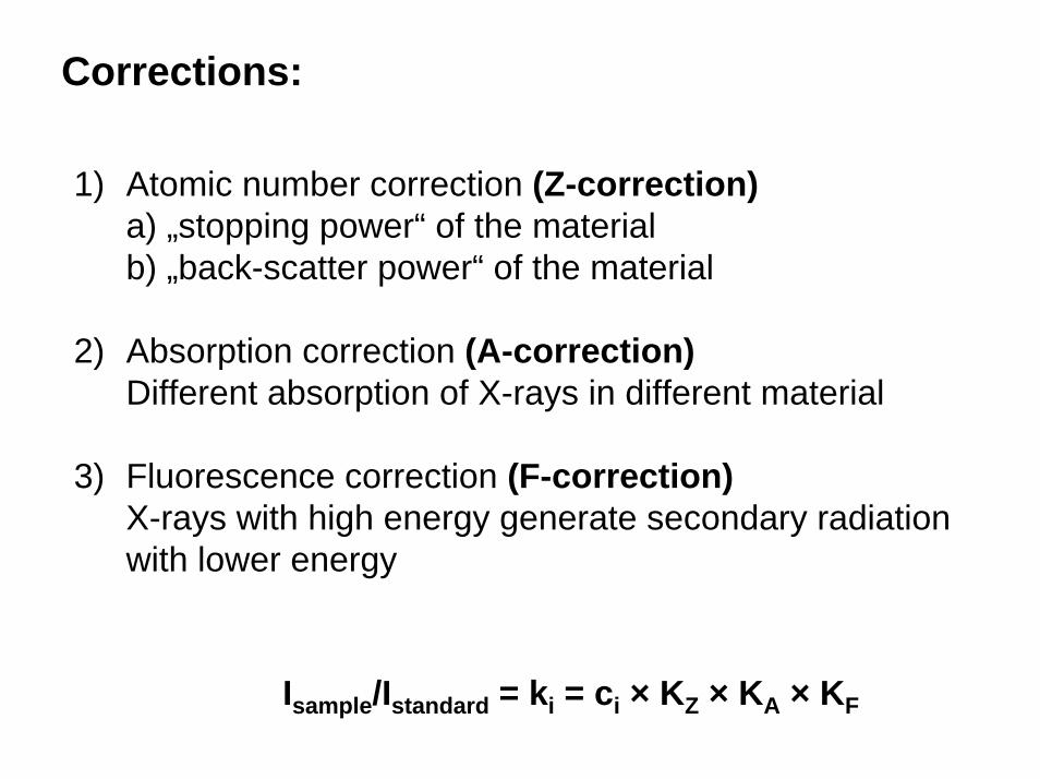
Corrections:
1) Atomic number correction (Z-correction)a) „stopping power“ of the materialb) „back-scatter power“ of the material
2) Absorption correction (A-correction)Different absorption of X-rays in different material
3) Fluorescence correction (F-correction)X-rays with high energy generate secondary radiationwith lower energy
Isample/Istandard = ki = ci × KZ × KA × KF
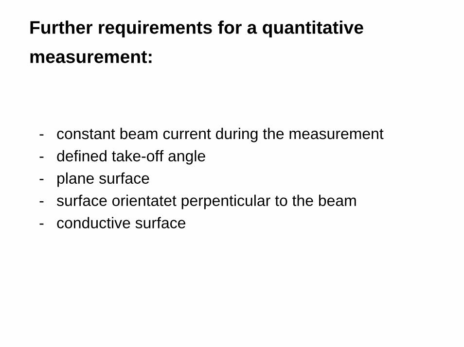
Further requirements for a quantitative
measurement:
- constant beam current during the measurement
- defined take-off angle
- plane surface
- surface orientatet perpenticular to the beam
- conductive surface