Embed Size (px)
Citation preview
Lecture 2
Microprocessor Architecture
Image from: http://micro.magnet.fsu.edu/chipshots/intel/images/intel8080dielarge.jpg
Agenda
Microprocessor components The memory Internal organization of MPU Introducing MARIE
Source Homework
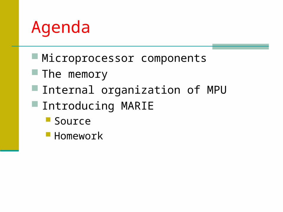
Von Neumann Model (Revisited)
Control Unit
ALU
Main Memory
Mass Memory
Input Output
Memory
CPU
Input Bus Output Bus
Data Bus

CPU Components
Arithmetic Logic Unit (ALU) Performs A & L ops on the data passing through it.
Addition, subtraction Logical AND, OR, shift ops
Control Unit (CU) Sequences the ops of the entire system
Fetch, decode, execute the successive instructions of a program stored in the memory.
Generate signals to synchronize operations There are 3 buses used to interconnect a system
Address buses, data buses, and control buses
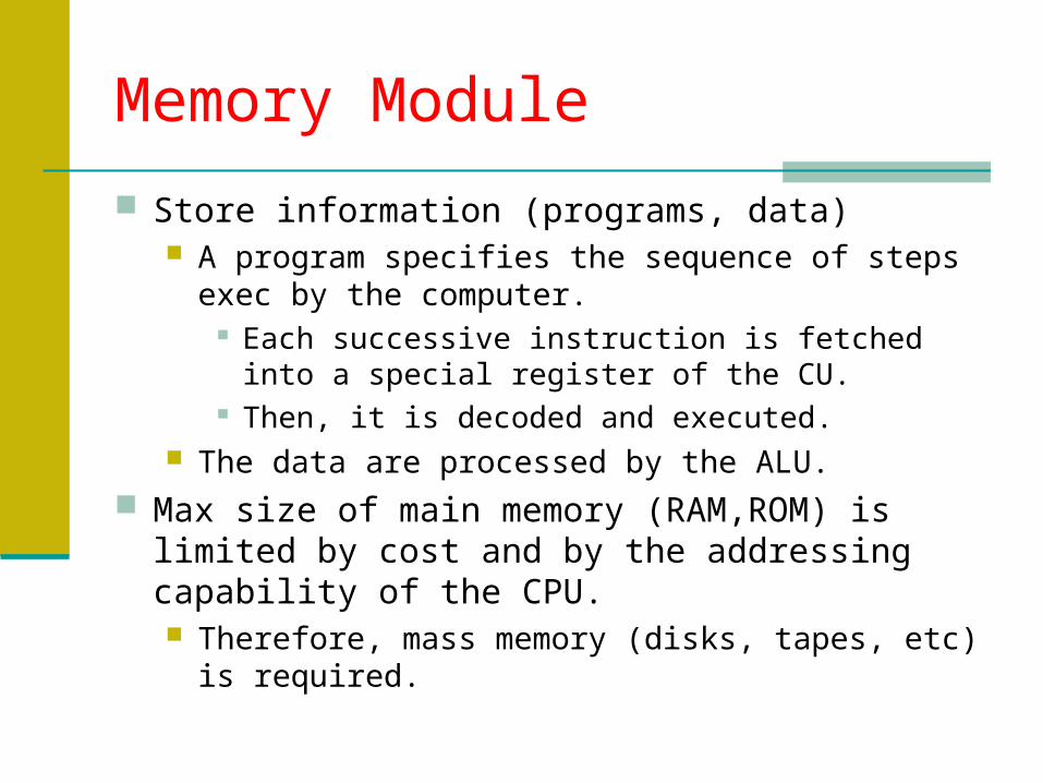
Memory Module
Store information (programs, data) A program specifies the sequence of steps exec by the
computer. Each successive instruction is fetched into a special
register of the CU. Then, it is decoded and executed.
The data are processed by the ALU. Max size of main memory (RAM,ROM) is limited by
cost and by the addressing capability of the CPU. Therefore, mass memory (disks, tapes, etc) is
required.

Input/Output Modules
They are used to communicate with the outside world. Input supplies information to the ALU, or the
memory. Keyboard, mouse, sensors, etc.
Output displays the data coming out of the ALU or executes commands.
Printer, control mechanism (motor, relay), etc.

The Buses
Data bus Transmits data between units Bidirectional Bus width typically equals to microprocessor’s bit-width (i.e.
8-bit MPU has 8-bit wide data bus) Address bus
Used to select the origin or destination of signal transmitted on another bus or line.
If there are 16 lines of address bus 64K addressable Control bus
Synchronizes the activities of the system. Carries status and control info both to and from the MPU
An effective bus design is crucial to the speed of the system.

A Simple Computer
LED Display
I/OInterface
Keyboard
CPU
Registers
Memory
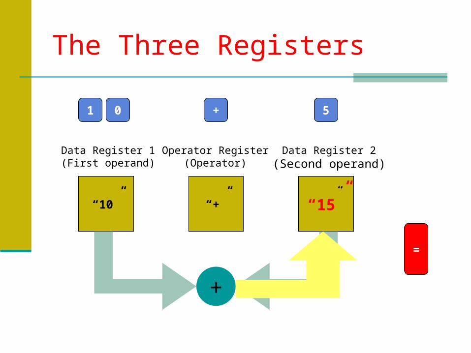
The Three Registers
“10” “+” “5”
1 0 + 5
=
Data Register 1(First operand)
Data Register 2(Second operand)
Operator Register(Operator)
+
“15”

The Memory
Memory Hierarchy Internal registers (fastest, lowest capacity)
Part of the ALU Main memory Mass memory (slowest, largest capacity)
Memory Access Logically organized in “words”.
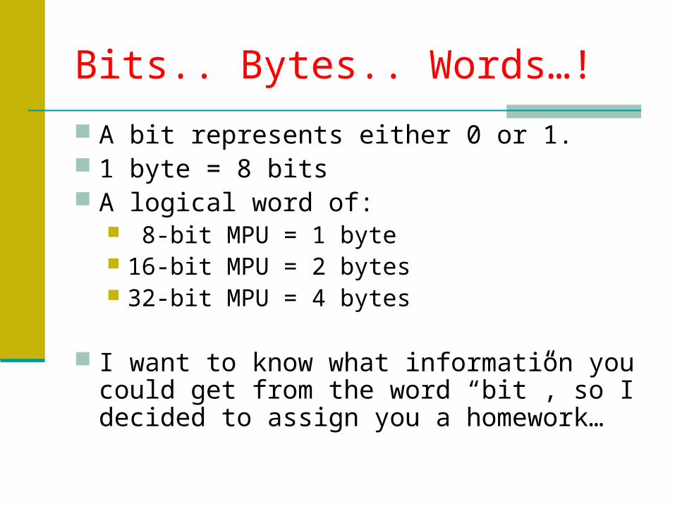
Bits.. Bytes.. Words…!
A bit represents either 0 or 1. 1 byte = 8 bits A logical word of:
8-bit MPU = 1 byte 16-bit MPU = 2 bytes 32-bit MPU = 4 bytes
I want to know what information you could get from the word “bit”, so I decided to assign you a homework…

Memory Access
Address 0
07Bit Position
Address (16 bits)
Address 65535
“P”
Address “P”
Data (8 bits)
Write / ReadControl signal
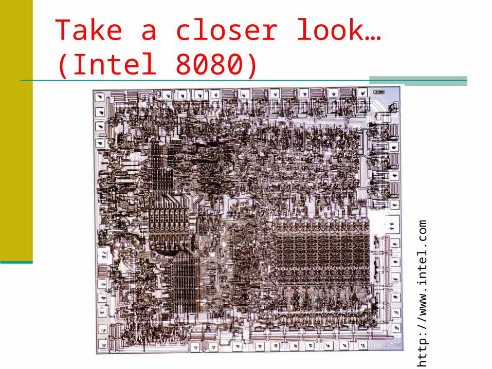
Take a closer look… (Intel 8080)
http
://w
ww
.inte
l.com
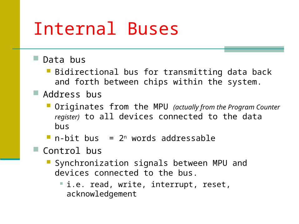
Internal Buses
Data bus Bidirectional bus for transmitting data back and forth
between chips within the system. Address bus
Originates from the MPU (actually from the Program Counter
register) to all devices connected to the data bus n-bit bus = 2n words addressable
Control bus Synchronization signals between MPU and devices
connected to the bus. i.e. read, write, interrupt, reset, acknowledgement
Architecture Category
The data bus is the bus that defines the architecture of a system.
Count the number of data buses used to communicate between the registers and the ALU
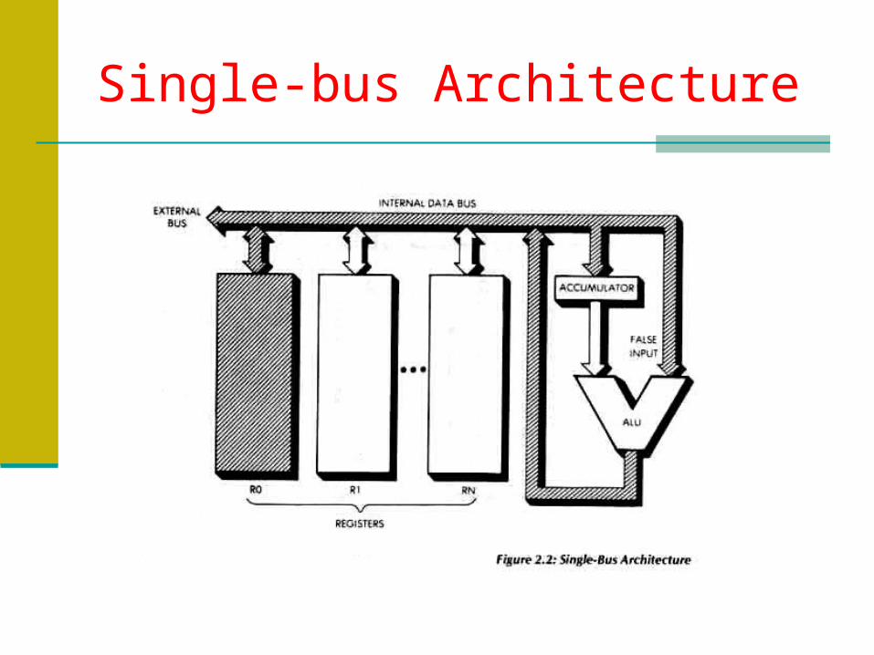
Single-bus Architecture
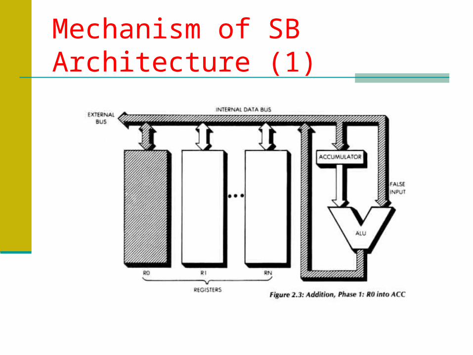
Mechanism of SB Architecture (1)
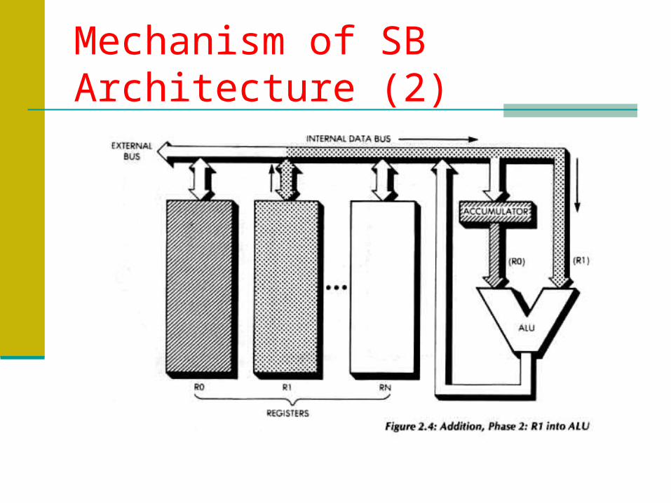
Mechanism of SB Architecture (2)

Mechanism of SB Architecture (3)
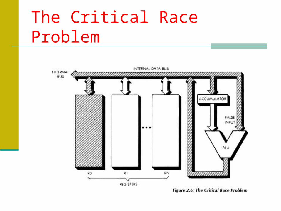
The Critical Race Problem
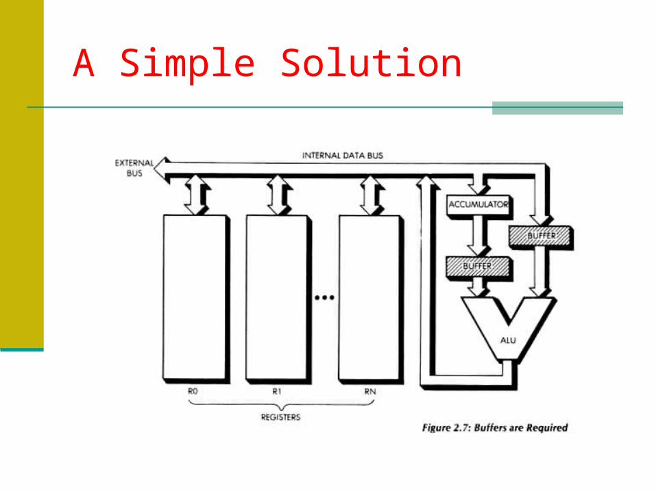
A Simple Solution

Double-Bus Architecture
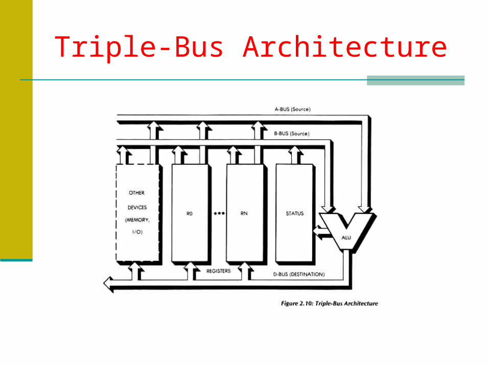
Triple-Bus Architecture
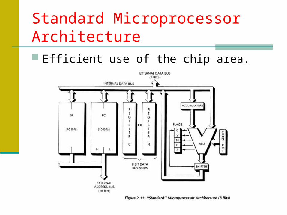
Standard Microprocessor Architecture
Efficient use of the chip area.
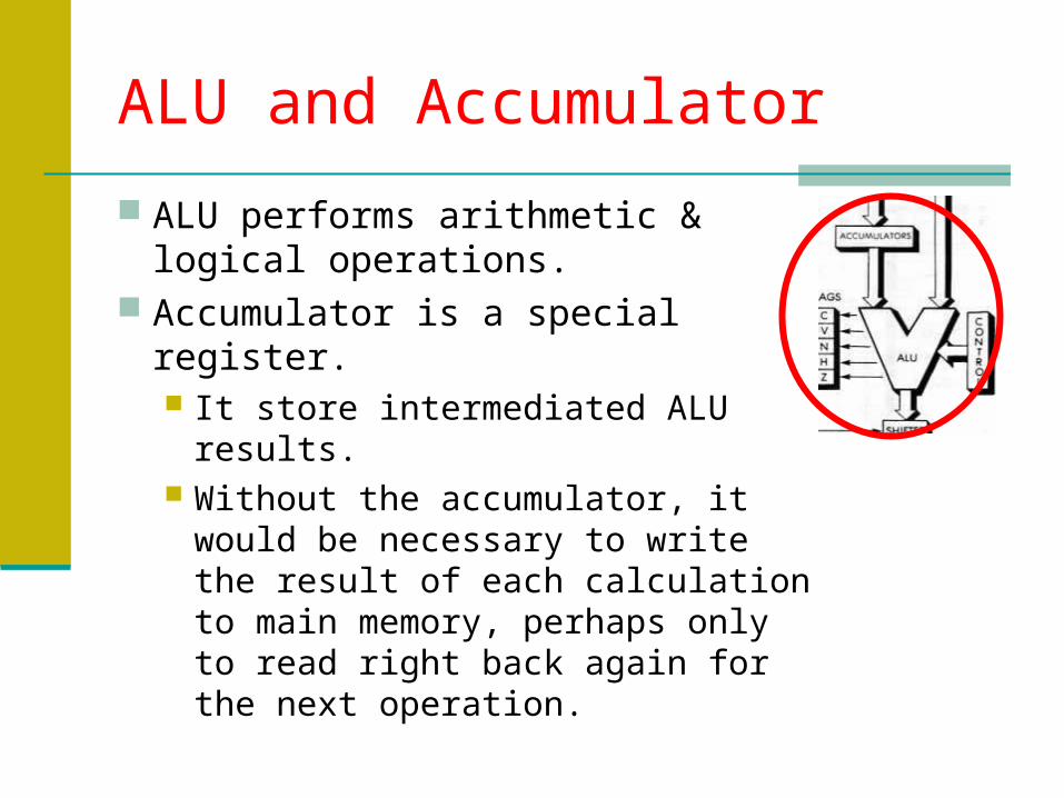
ALU and Accumulator
ALU performs arithmetic & logical operations.
Accumulator is a special register. It store intermediated ALU results. Without the accumulator, it would
be necessary to write the result of each calculation to main memory, perhaps only to read right back again for the next operation.

Shift and Rotate Facilities
The shifter performs shift and rotate operations.
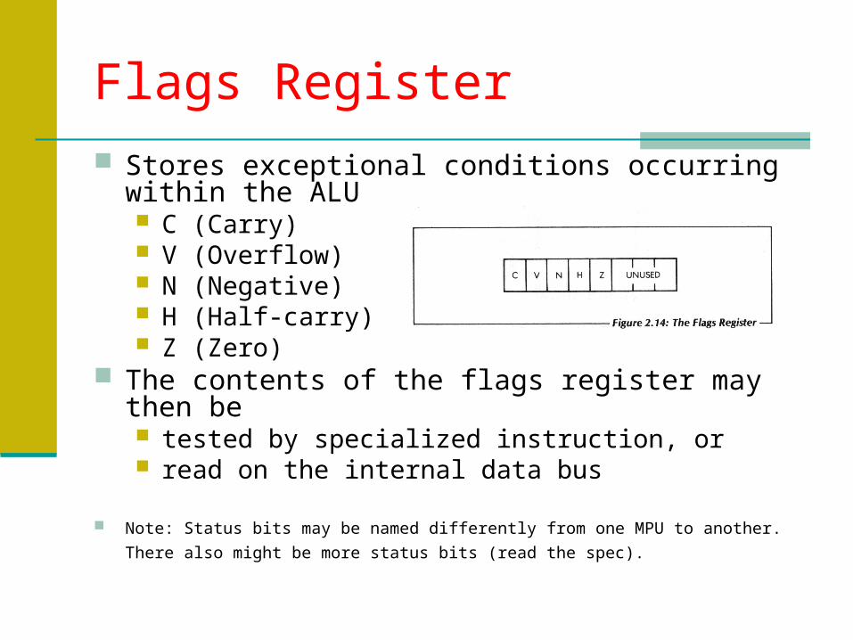
Flags Register
Stores exceptional conditions occurring within the ALU C (Carry) V (Overflow) N (Negative) H (Half-carry) Z (Zero)
The contents of the flags register may then be tested by specialized instruction, or read on the internal data bus
Note: Status bits may be named differently from one MPU to another. There also might be
more status bits (read the spec).
General-Purpose Registers
Fast memories provided that the ALU can manipulate data at high speed.
There are limited number of GPRs because of restrictions placed on the number of bits that it is reasonable to provide within an instruction.
Specific role of these registers is not defined in advance. They may be used to contain any data generated by the program.
Register-pairs facilitate to operate two of these registers simultaneously.
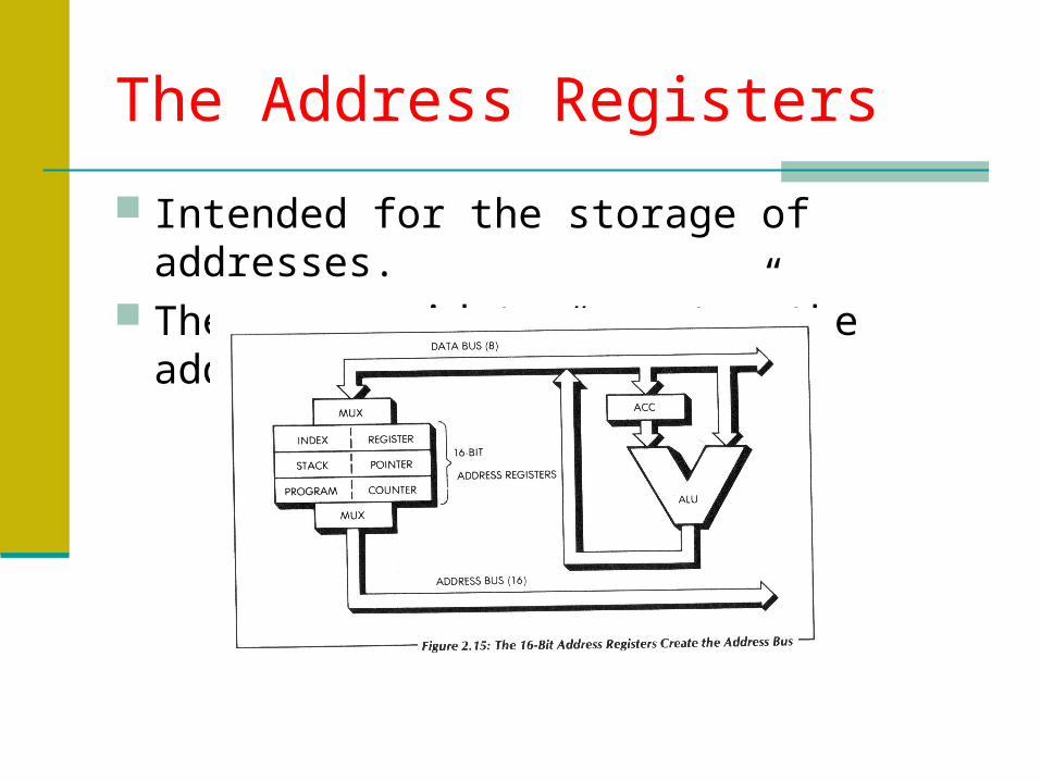
The Address Registers
Intended for the storage of addresses. They are said to “create” the address bus.
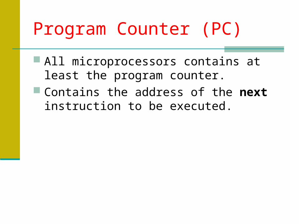
Program Counter (PC)
All microprocessors contains at least the program counter.
Contains the address of the next instruction to be executed.
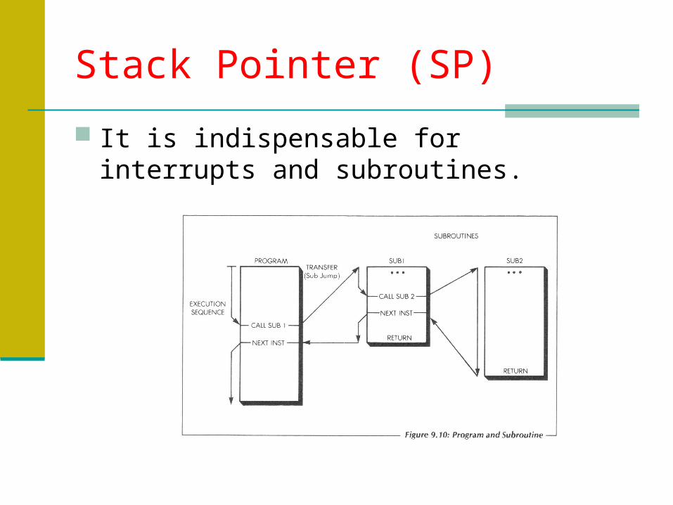
Stack Pointer (SP)
It is indispensable for interrupts and subroutines.
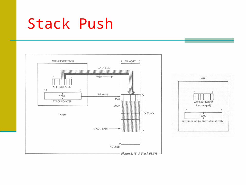
Stack Push
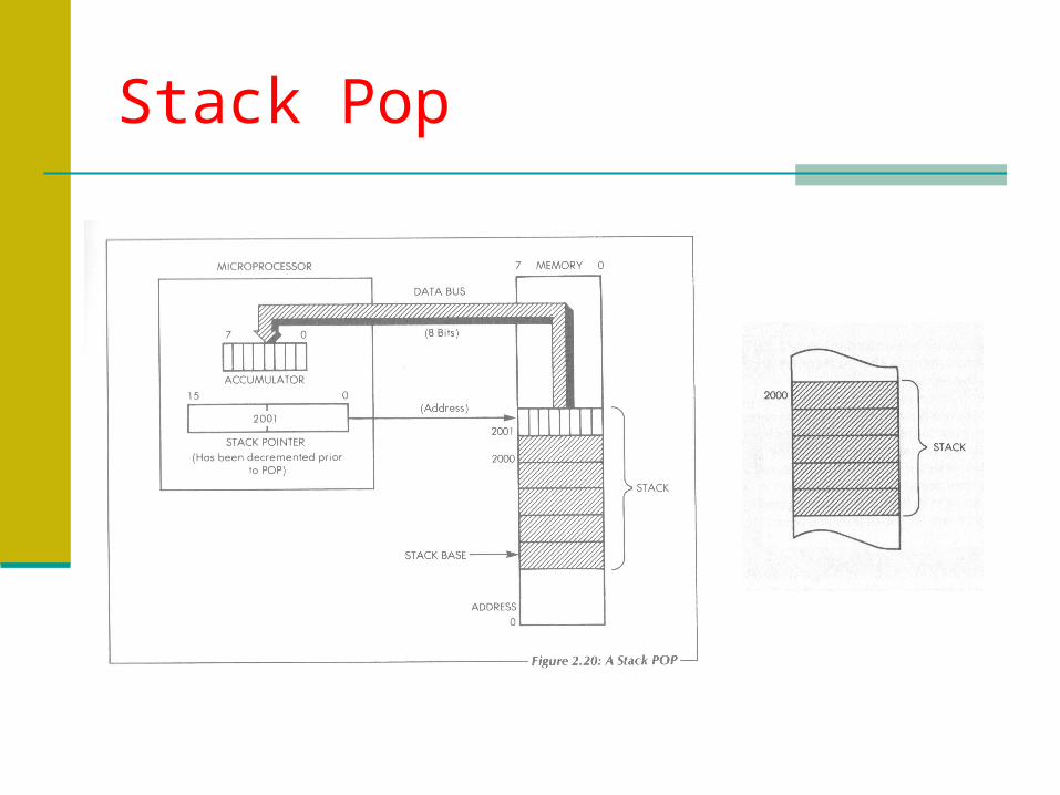
Stack Pop
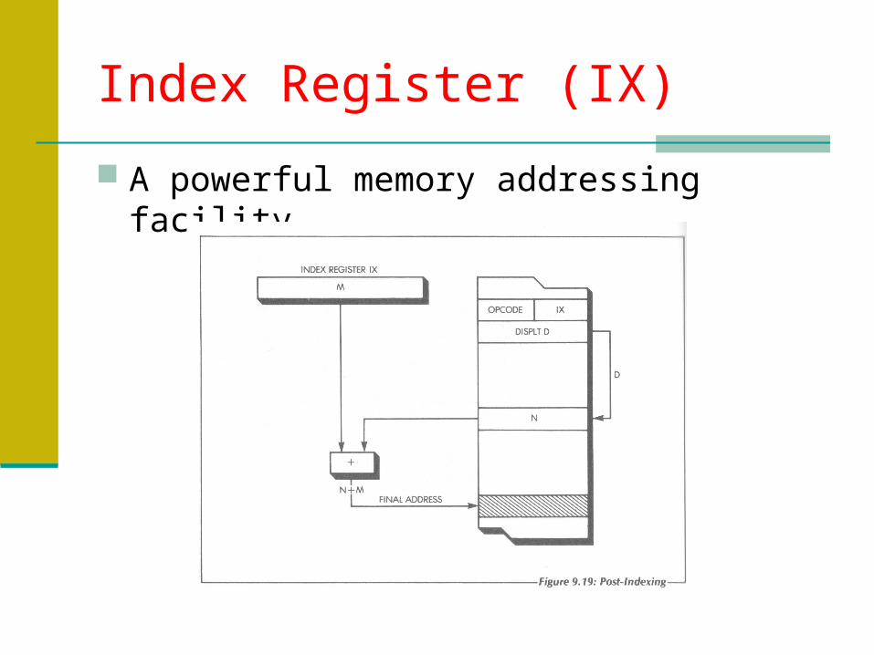
Index Register (IX)
A powerful memory addressing facility.

Disclaimer
Some diagrams in this slide are scanned and some are redrawn for teaching purpose only. They are in the book:
R. Zaks, From Chips to Systems: an Introduction to Microprocessors, Sybex, 1981.