Embed Size (px)
Citation preview
Introduction to
CMOS VLSI
Design
Lecture 2
Circuits and Layout
David Harris, Harvey Mudd College
Kartik Mohanram and Steven Levitan
University of Pittsburgh
CMOS VLSI Design1: Circuits & Layout Slide 2
Outline
A Brief History
CMOS Gate Design
Pass Transistors
CMOS Latches & Flip-Flops
Standard Cell Layouts
Stick Diagrams
CMOS VLSI Design1: Circuits & Layout Slide 3
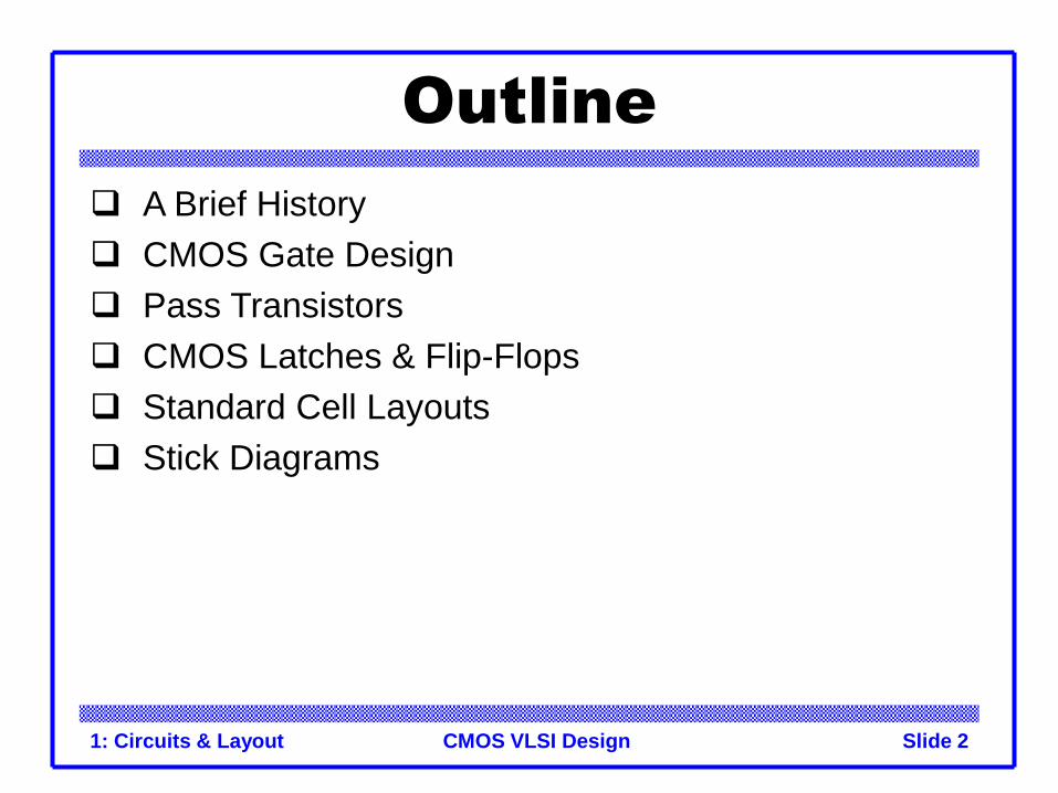
A Brief History
1958: First integrated circuit
– Flip-flop using two transistors
– Built by Jack Kilby at Texas Instruments
2003
– Intel Pentium 4 mprocessor (55 million transistors)
– 512 Mbit DRAM (> 0.5 billion transistors)
53% compound annual growth rate over 45 years
– No other technology has grown so fast so long
Driven by miniaturization of transistors
– Smaller is cheaper, faster, lower in power!
– Revolutionary effects on society

CMOS VLSI Design1: Circuits & Layout Slide 4
Annual Sales
1018 transistors manufactured in 2003
– 100 million for every human on the planet
0
50
100
150
200
1982 1984 1986 1988 1990 1992 1994 1996 1998 2000 2002
Year
Glo
bal S
em
iconducto
r Billin
gs
(Billio
ns o
f US
$)
CMOS VLSI Design1: Circuits & Layout Slide 5
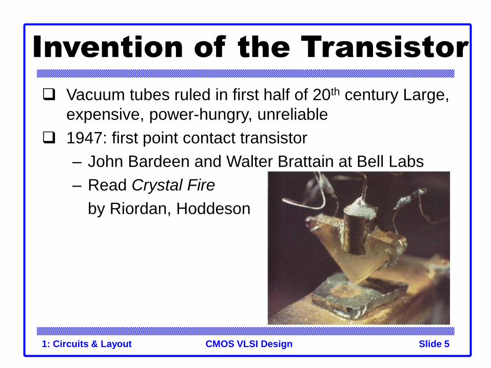
Invention of the Transistor
Vacuum tubes ruled in first half of 20th century Large,
expensive, power-hungry, unreliable
1947: first point contact transistor
– John Bardeen and Walter Brattain at Bell Labs
– Read Crystal Fire
by Riordan, Hoddeson
CMOS VLSI Design1: Circuits & Layout Slide 6
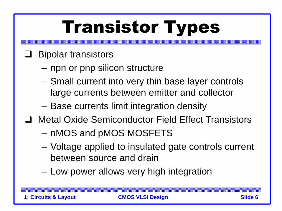
Transistor Types
Bipolar transistors
– npn or pnp silicon structure
– Small current into very thin base layer controls
large currents between emitter and collector
– Base currents limit integration density
Metal Oxide Semiconductor Field Effect Transistors
– nMOS and pMOS MOSFETS
– Voltage applied to insulated gate controls current
between source and drain
– Low power allows very high integration
CMOS VLSI Design1: Circuits & Layout Slide 7
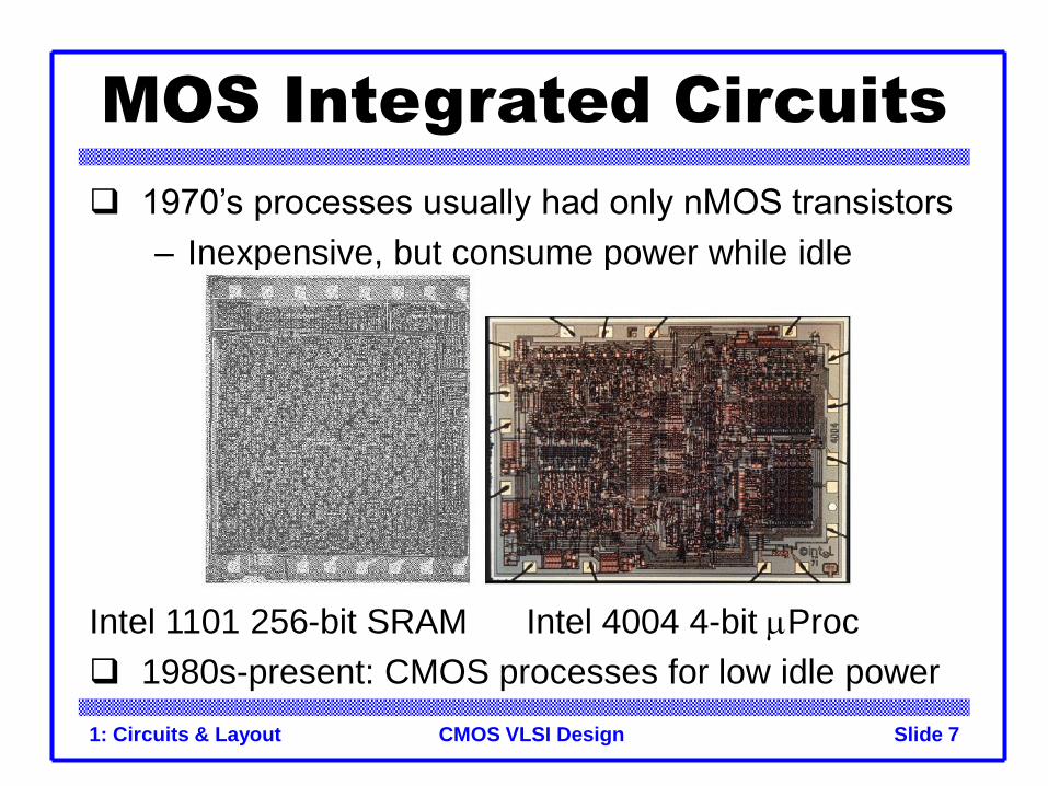
1970’s processes usually had only nMOS transistors
– Inexpensive, but consume power while idle
1980s-present: CMOS processes for low idle power
MOS Integrated Circuits
Intel 1101 256-bit SRAM Intel 4004 4-bit mProc
CMOS VLSI Design1: Circuits & Layout Slide 8
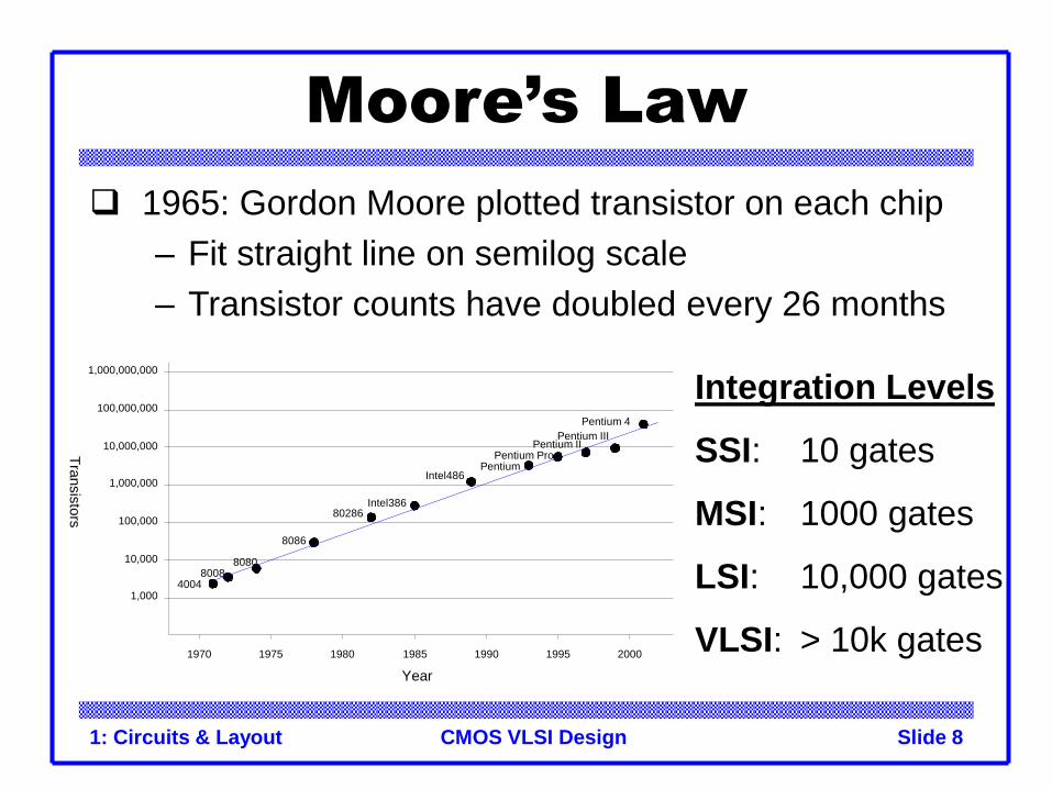
Moore’s Law
1965: Gordon Moore plotted transistor on each chip
– Fit straight line on semilog scale
– Transistor counts have doubled every 26 months
Year
Tra
nsis
tors
40048008
8080
8086
80286Intel386
Intel486Pentium
Pentium ProPentium II
Pentium III
Pentium 4
1,000
10,000
100,000
1,000,000
10,000,000
100,000,000
1,000,000,000
1970 1975 1980 1985 1990 1995 2000
Integration Levels
SSI: 10 gates
MSI: 1000 gates
LSI: 10,000 gates
VLSI: > 10k gates
CMOS VLSI Design1: Circuits & Layout Slide 9
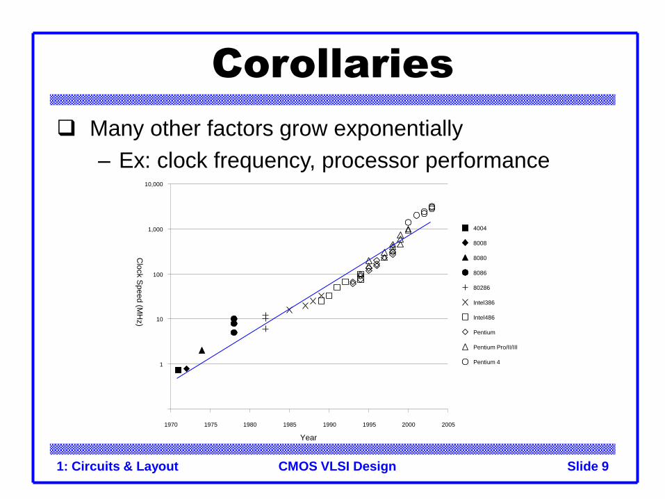
Corollaries
Many other factors grow exponentially
– Ex: clock frequency, processor performance
Year
1
10
100
1,000
10,000
1970 1975 1980 1985 1990 1995 2000 2005
4004
8008
8080
8086
80286
Intel386
Intel486
Pentium
Pentium Pro/II/III
Pentium 4
Clo
ck S
peed (M
Hz)
EE141© Digital Integrated Circuits2nd Manufacturing10
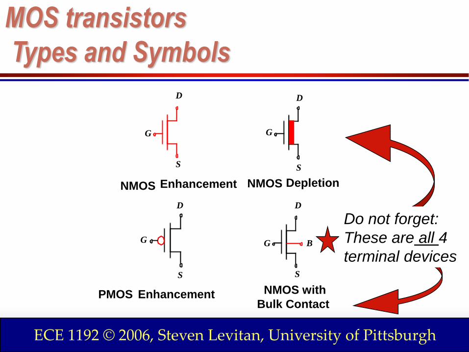
MOS transistors
Types and Symbols
D
S
G
D
S
G
G
S
D D
S
G
NMOS Enhancement NMOS
PMOS
Depletion
Enhancement
B
NMOS with
Bulk Contact
Digital Integrated Circuits © Prentice Hall 1995IntroductionECE 1192 © 2006, Steven Levitan, University of Pittsburgh
Do not forget:
These are all 4
terminal devices
EE141© Digital Integrated Circuits2nd Manufacturing11
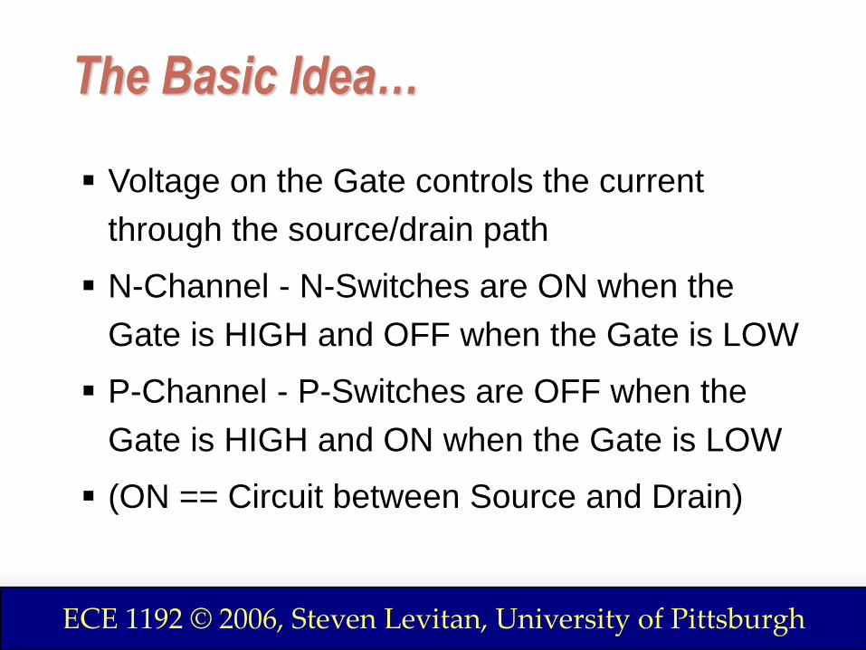
The Basic Idea…
▪ Voltage on the Gate controls the current
through the source/drain path
▪ N-Channel - N-Switches are ON when the
Gate is HIGH and OFF when the Gate is LOW
▪ P-Channel - P-Switches are OFF when the
Gate is HIGH and ON when the Gate is LOW
▪ (ON == Circuit between Source and Drain)
ECE 1192 © 2006, Steven Levitan, University of Pittsburgh
EE141© Digital Integrated Circuits2nd Manufacturing12
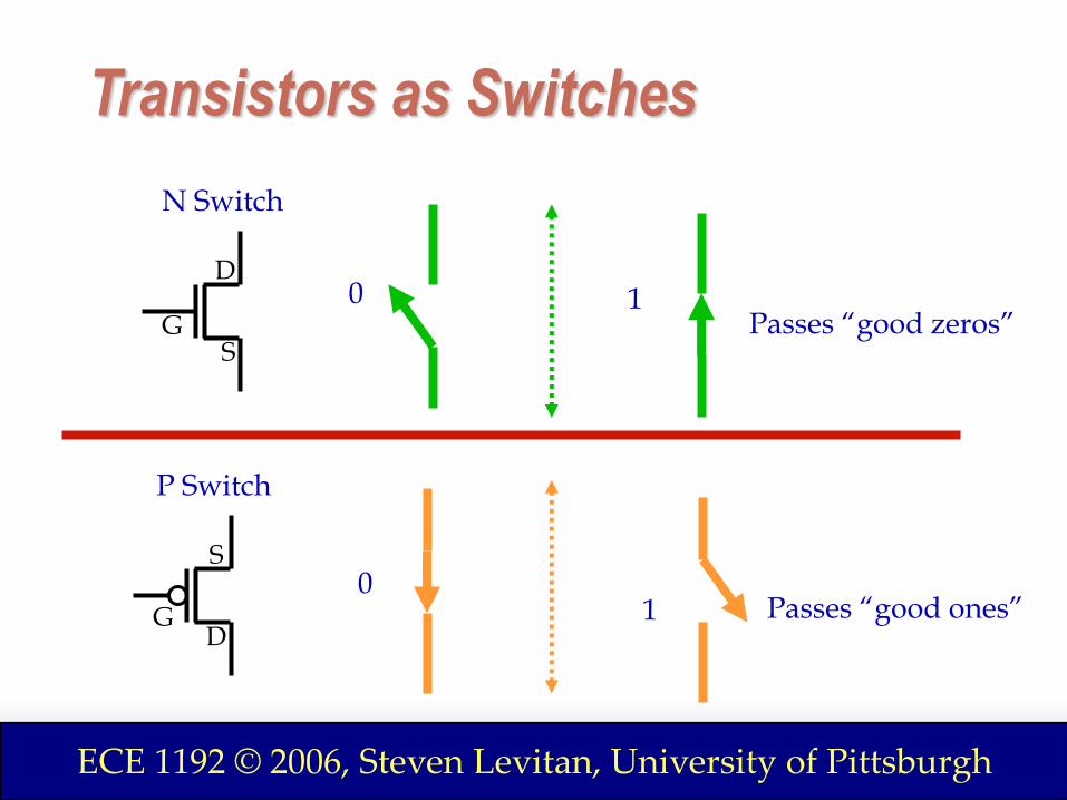
Transistors as Switches
GS
D
GD
S
N Switch
P Switch
0
1
1
0
Passes “good zeros”
Passes “good ones”
ECE 1192 © 2006, Steven Levitan, University of Pittsburgh
EE141© Digital Integrated Circuits2nd Manufacturing13
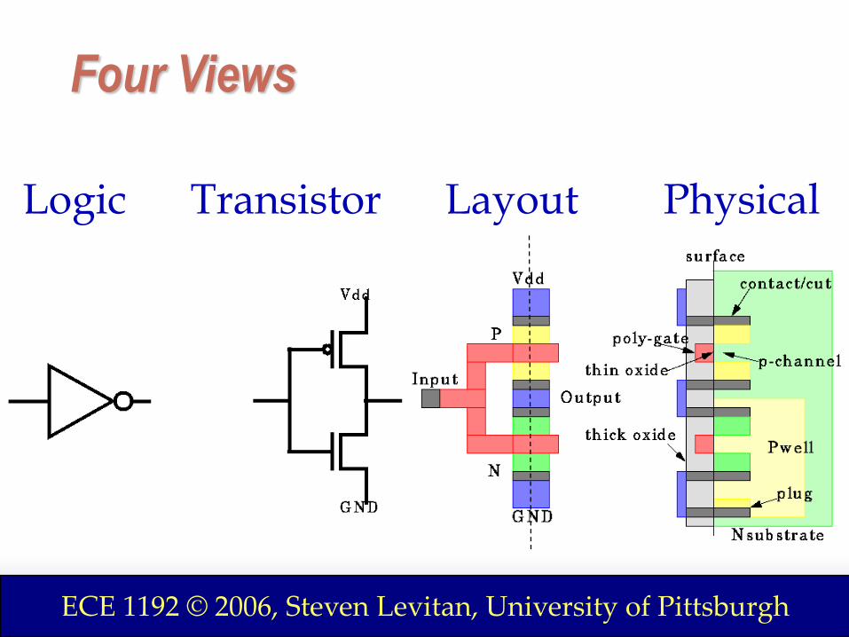
Four Views
Logic Transistor Layout Physical
ECE 1192 © 2006, Steven Levitan, University of Pittsburgh
EE141© Digital Integrated Circuits2nd Manufacturing14
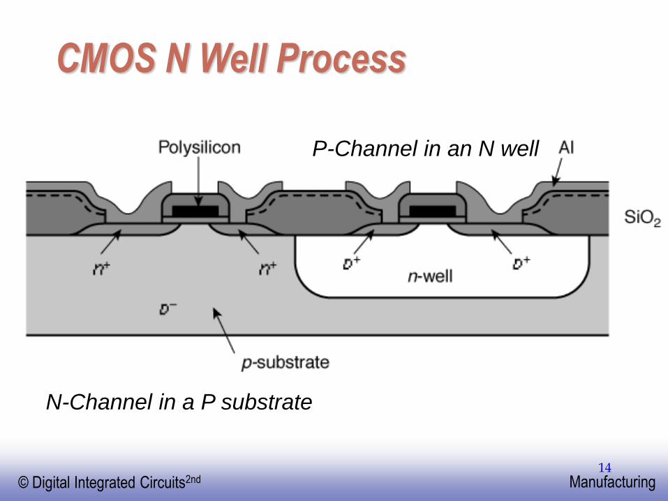
CMOS N Well Process
P-Channel in an N well
N-Channel in a P substrate
EE141© Digital Integrated Circuits2nd Manufacturing15
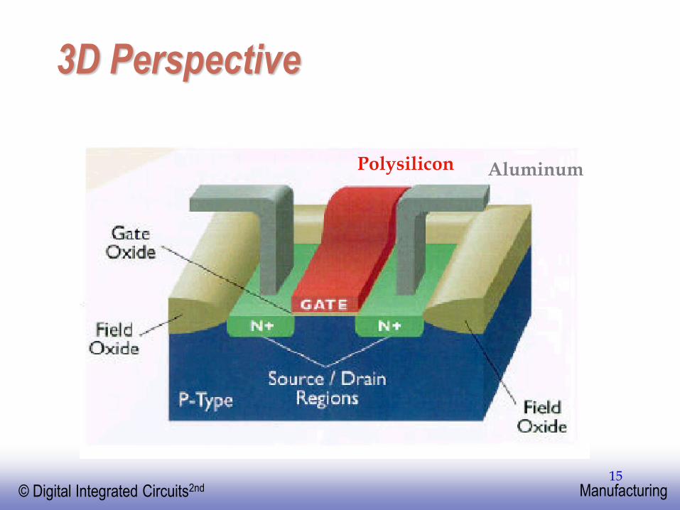
3D Perspective
Polysilicon Aluminum
EE141© Digital Integrated Circuits2nd Manufacturing16
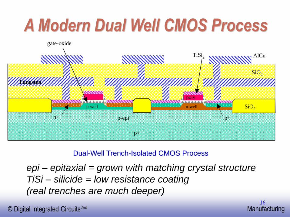
A Modern Dual Well CMOS Process
p-well n-well
p+
p-epi
SiO2
AlCu
poly
n+
SiO2
p+
gate-oxide
Tungsten
TiSi2
Dual-Well Trench-Isolated CMOS Process
epi – epitaxial = grown with matching crystal structure
TiSi – silicide = low resistance coating
(real trenches are much deeper)
CMOS VLSI Design1: Circuits & Layout Slide 17
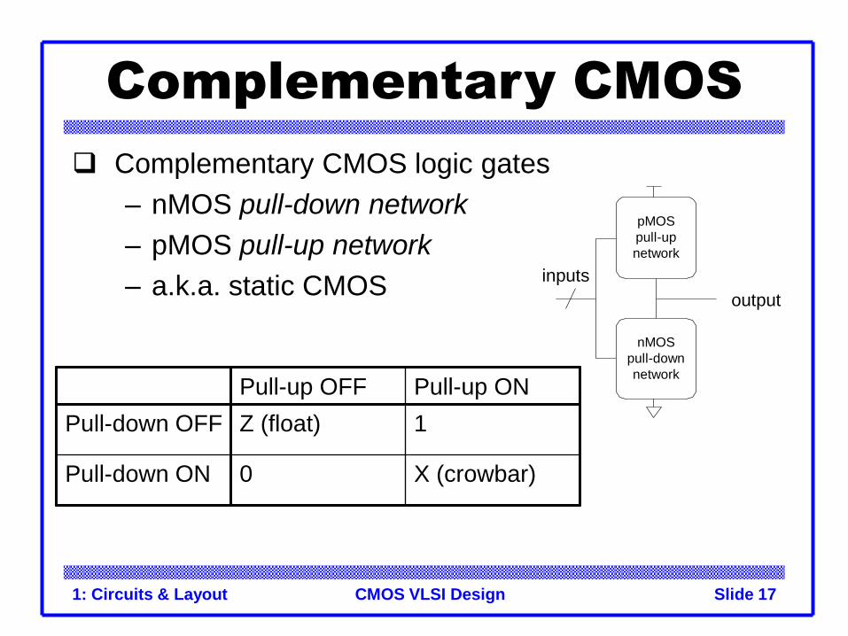
Complementary CMOS
Complementary CMOS logic gates
– nMOS pull-down network
– pMOS pull-up network
– a.k.a. static CMOS
pMOS
pull-up
network
output
inputs
nMOS
pull-down
network
Pull-up OFF Pull-up ON
Pull-down OFF Z (float) 1
Pull-down ON 0 X (crowbar)
CMOS VLSI Design1: Circuits & Layout Slide 18
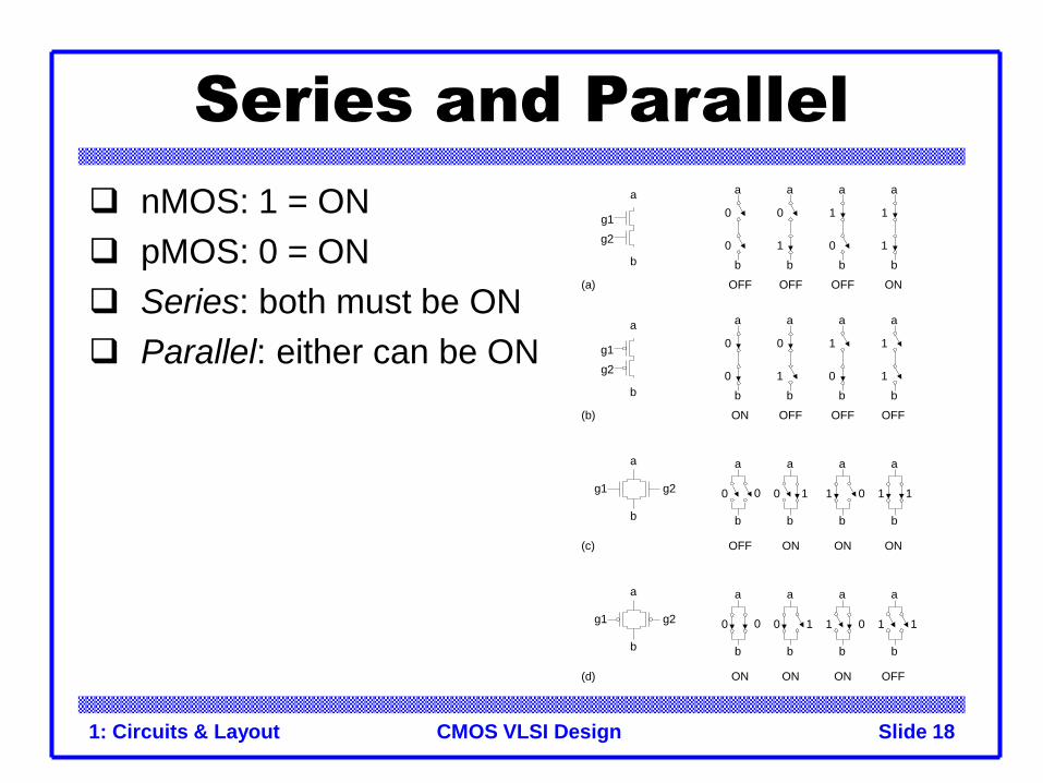
Series and Parallel
nMOS: 1 = ON
pMOS: 0 = ON
Series: both must be ON
Parallel: either can be ON
(a)
a
b
a
b
g1
g2
0
0
a
b
0
1
a
b
1
0
a
b
1
1
OFF OFF OFF ON
(b)
a
b
a
b
g1
g2
0
0
a
b
0
1
a
b
1
0
a
b
1
1
ON OFF OFF OFF
(c)
a
b
a
b
g1 g2 0 0
OFF ON ON ON
(d) ON ON ON OFF
a
b
0
a
b
1
a
b
11 0 1
a
b
0 0
a
b
0
a
b
1
a
b
11 0 1
a
b
g1 g2
CMOS VLSI Design1: Circuits & Layout Slide 19
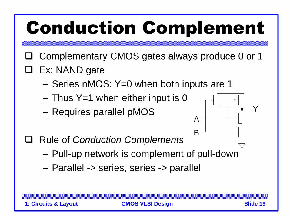
Conduction Complement
Complementary CMOS gates always produce 0 or 1
Ex: NAND gate
– Series nMOS: Y=0 when both inputs are 1
– Thus Y=1 when either input is 0
– Requires parallel pMOS
Rule of Conduction Complements
– Pull-up network is complement of pull-down
– Parallel -> series, series -> parallel
A
B
Y
CMOS VLSI Design1: Circuits & Layout Slide 20
CMOS Gate Design
Activity:
– Sketch a 4-input CMOS NAND gate
CMOS VLSI Design1: Circuits & Layout Slide 21
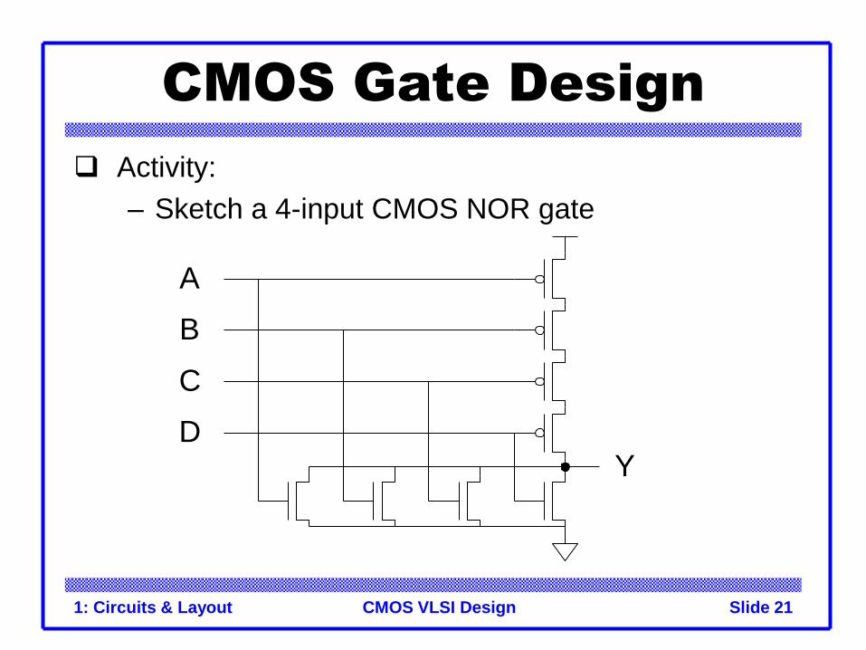
CMOS Gate Design
Activity:
– Sketch a 4-input CMOS NOR gate
A
B
C
DY
CMOS VLSI Design1: Circuits & Layout Slide 22
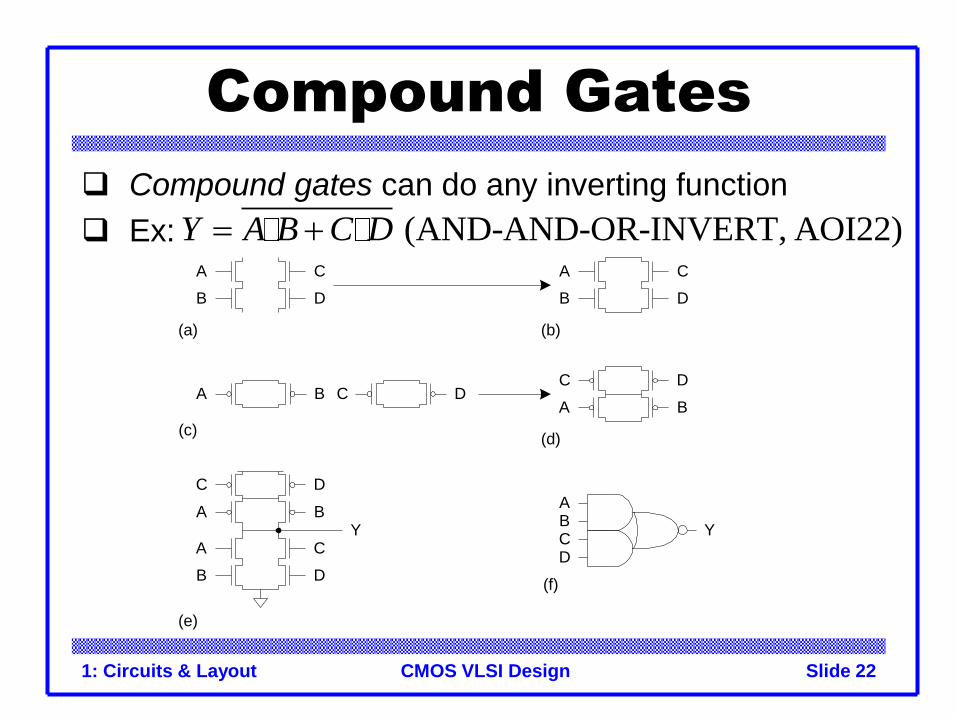
Compound Gates
Compound gates can do any inverting function
Ex: (AND-AND-OR-INVERT, AOI22)Y A B C D A
B
C
D
A
B
C
D
A B C DA B
C D
B
D
YA
CA
C
A
B
C
D
B
D
Y
(a)
(c)
(e)
(b)
(d)
(f)
CMOS VLSI Design1: Circuits & Layout Slide 23
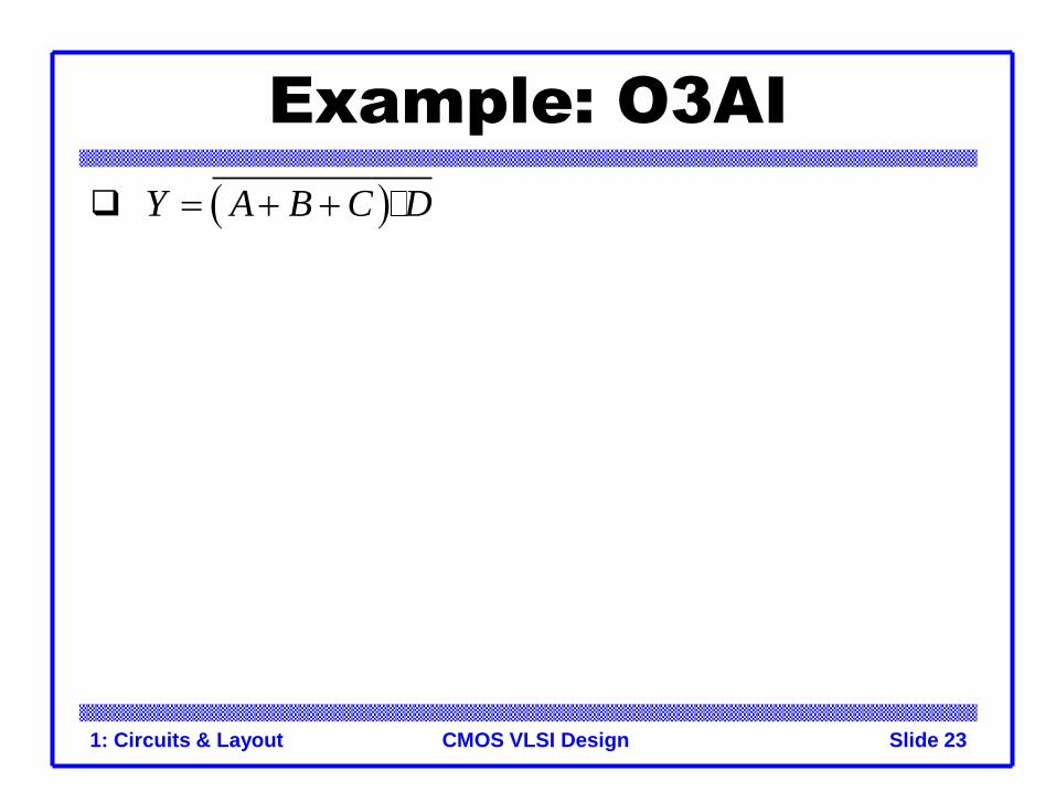
Example: O3AI
Y A B C D
CMOS VLSI Design1: Circuits & Layout Slide 24
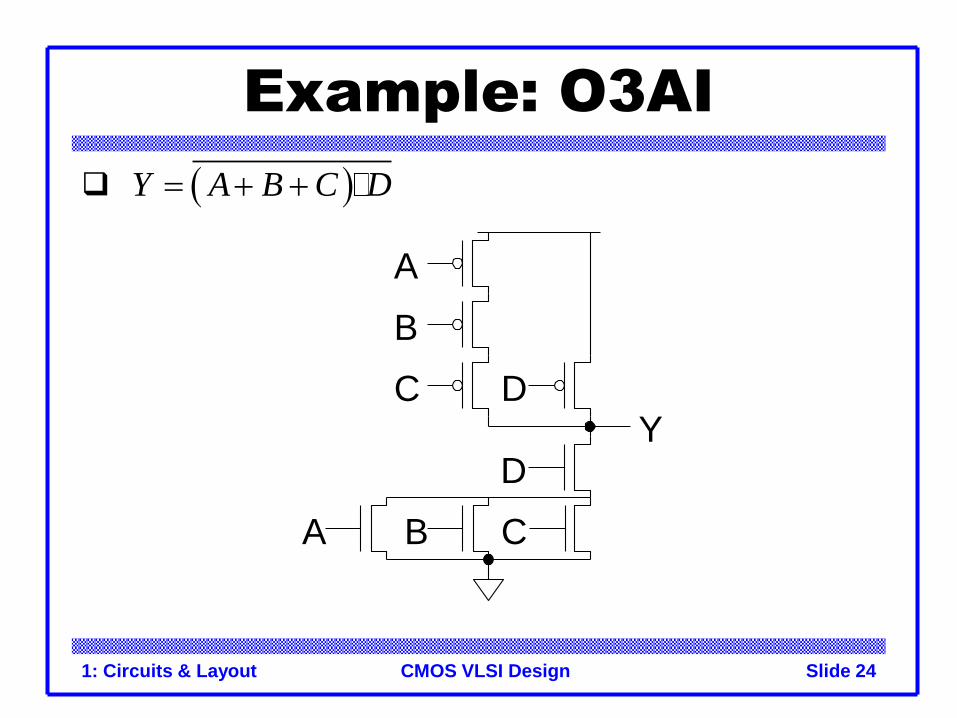
Example: O3AI
Y A B C D
A B
Y
C
D
DC
B
A
CMOS VLSI Design1: Circuits & Layout Slide 25
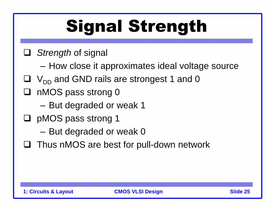
Signal Strength
Strength of signal
– How close it approximates ideal voltage source
VDD and GND rails are strongest 1 and 0
nMOS pass strong 0
– But degraded or weak 1
pMOS pass strong 1
– But degraded or weak 0
Thus nMOS are best for pull-down network

CMOS VLSI Design1: Circuits & Layout Slide 26
Pass Transistors
Transistors can be used as switches
g
s d
g
s d
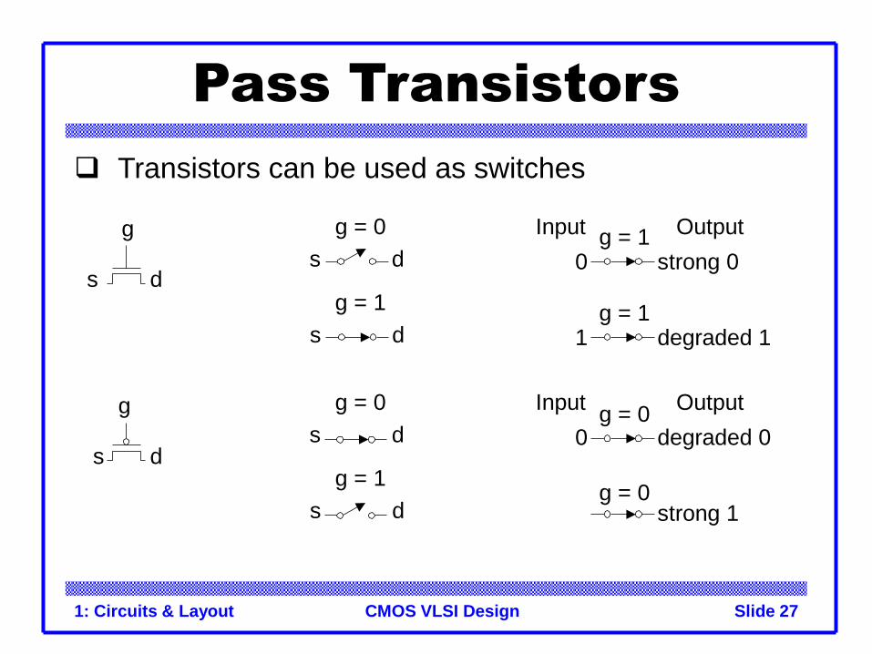
CMOS VLSI Design1: Circuits & Layout Slide 27
Pass Transistors
Transistors can be used as switches
g
s d
g = 0
s d
g = 1
s d
0 strong 0
Input Output
1 degraded 1
g
s d
g = 0
s d
g = 1
s d
0 degraded 0
Input Output
strong 1
g = 1
g = 1
g = 0
g = 0
CMOS VLSI Design1: Circuits & Layout Slide 28
Transmission Gates
Pass transistors produce degraded outputs
Transmission gates pass both 0 and 1 well
CMOS VLSI Design1: Circuits & Layout Slide 29
Transmission Gates
Pass transistors produce degraded outputs
Transmission gates pass both 0 and 1 well
g = 0, gb = 1
a b
g = 1, gb = 0
a b
0 strong 0
Input Output
1 strong 1
g
gb
a b
a b
g
gb
a b
g
gb
a b
g
gb
g = 1, gb = 0
g = 1, gb = 0
CMOS VLSI Design1: Circuits & Layout Slide 30
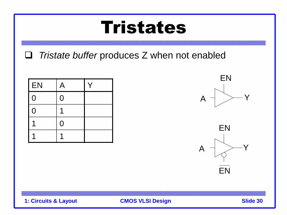
Tristates
Tristate buffer produces Z when not enabled
EN A Y
0 0
0 1
1 0
1 1
A Y
EN
A Y
EN
EN
CMOS VLSI Design1: Circuits & Layout Slide 31
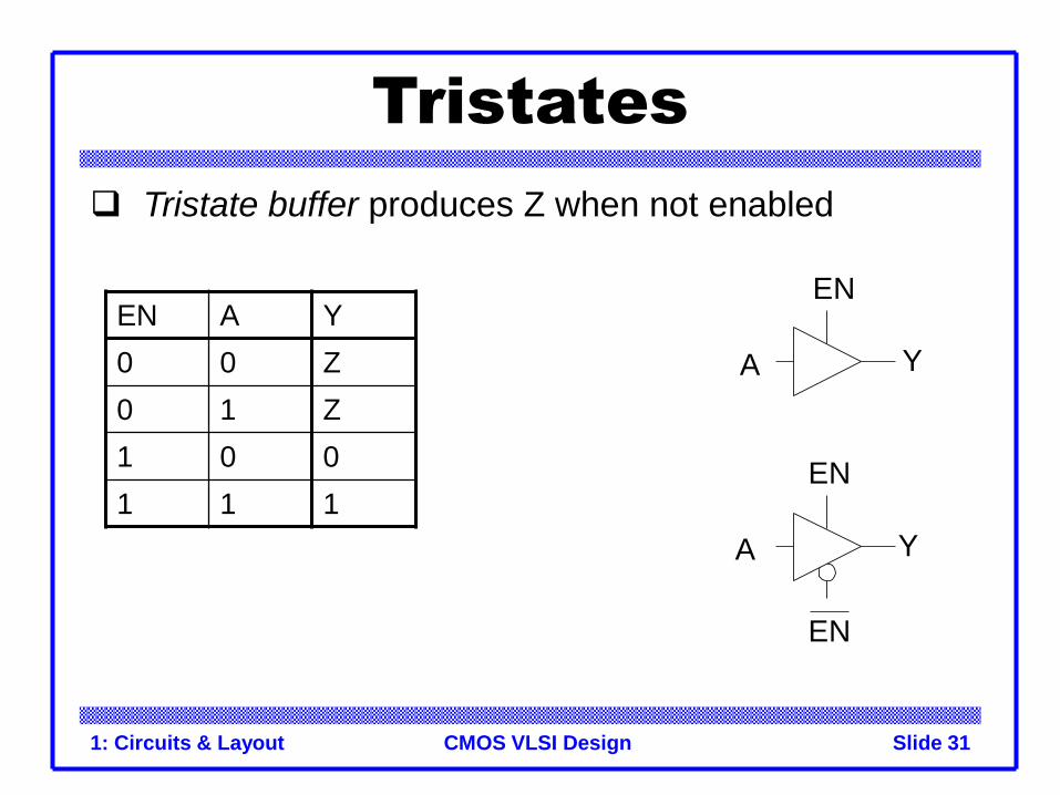
Tristates
Tristate buffer produces Z when not enabled
EN A Y
0 0 Z
0 1 Z
1 0 0
1 1 1
A Y
EN
A Y
EN
EN
CMOS VLSI Design1: Circuits & Layout Slide 32
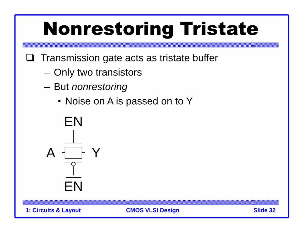
Nonrestoring Tristate
Transmission gate acts as tristate buffer
– Only two transistors
– But nonrestoring
• Noise on A is passed on to Y
A Y
EN
EN
CMOS VLSI Design1: Circuits & Layout Slide 33
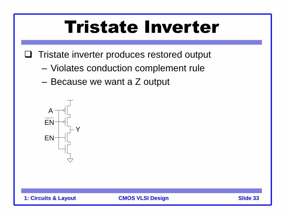
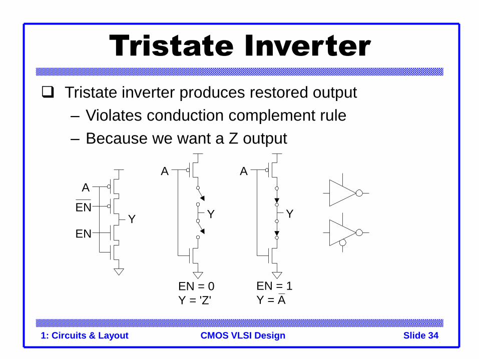
Tristate Inverter
Tristate inverter produces restored output
– Violates conduction complement rule
– Because we want a Z output
A
Y
EN
EN
CMOS VLSI Design1: Circuits & Layout Slide 34
Tristate Inverter
Tristate inverter produces restored output
– Violates conduction complement rule
– Because we want a Z output
A
Y
EN
A
Y
EN = 0
Y = 'Z'
Y
EN = 1
Y = A
A
EN
CMOS VLSI Design1: Circuits & Layout Slide 35
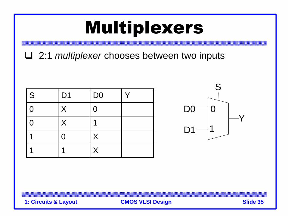
Multiplexers
2:1 multiplexer chooses between two inputs
S D1 D0 Y
0 X 0
0 X 1
1 0 X
1 1 X
0
1
S
D0
D1
Y
CMOS VLSI Design1: Circuits & Layout Slide 36
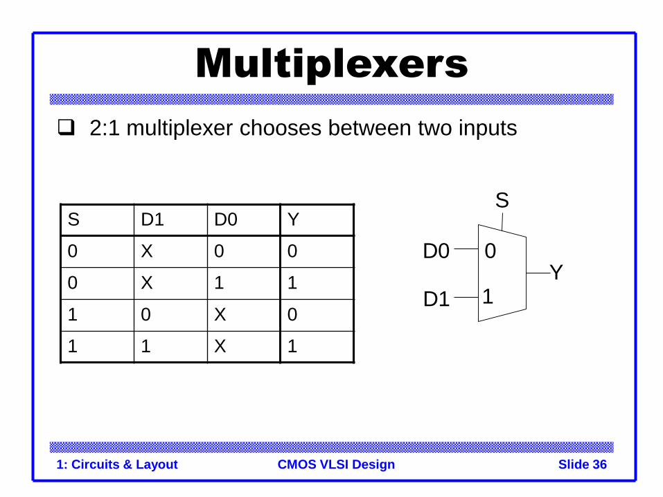
Multiplexers
2:1 multiplexer chooses between two inputs
S D1 D0 Y
0 X 0 0
0 X 1 1
1 0 X 0
1 1 X 1
0
1
S
D0
D1
Y
CMOS VLSI Design1: Circuits & Layout Slide 37
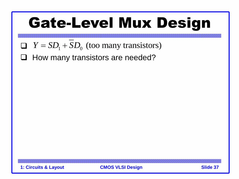
Gate-Level Mux Design
How many transistors are needed?
1 0 (too many transistors)Y SD SD
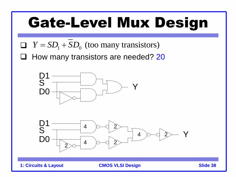
CMOS VLSI Design1: Circuits & Layout Slide 38
Gate-Level Mux Design
How many transistors are needed? 20
1 0 (too many transistors)Y SD SD
4
4
D1
D0S
Y
4
2
2
2 Y
2
D1
D0S
CMOS VLSI Design1: Circuits & Layout Slide 39
Transmission Gate Mux
Nonrestoring mux uses two transmission gates
CMOS VLSI Design1: Circuits & Layout Slide 40
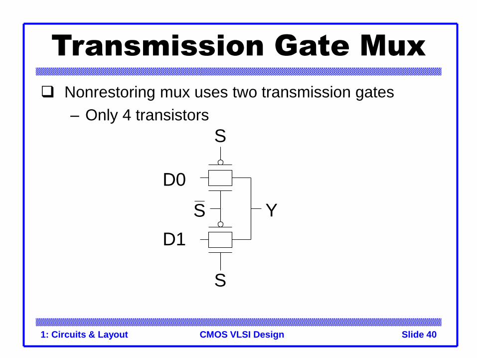
Transmission Gate Mux
Nonrestoring mux uses two transmission gates
– Only 4 transistors
S
S
D0
D1
YS
CMOS VLSI Design1: Circuits & Layout Slide 41
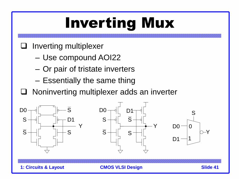
Inverting Mux
Inverting multiplexer
– Use compound AOI22
– Or pair of tristate inverters
– Essentially the same thing
Noninverting multiplexer adds an inverter
S
D0 D1
Y
S
D0
D1
Y0
1S
Y
D0
D1
S
S
S
S
S
S
CMOS VLSI Design1: Circuits & Layout Slide 42
4:1 Multiplexer
4:1 mux chooses one of 4 inputs using two selects
CMOS VLSI Design1: Circuits & Layout Slide 43
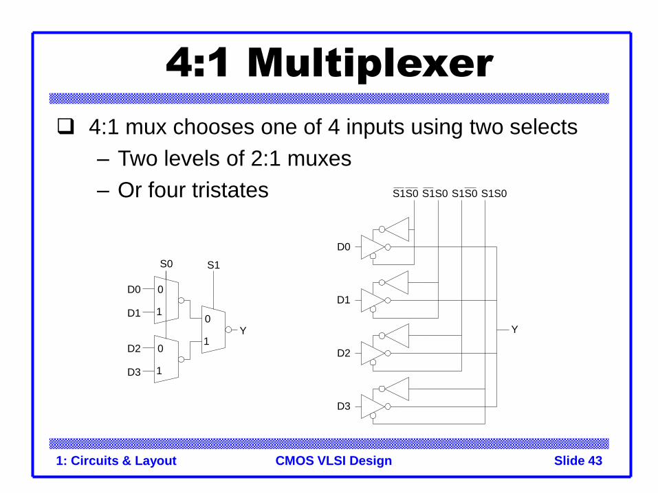
4:1 Multiplexer
4:1 mux chooses one of 4 inputs using two selects
– Two levels of 2:1 muxes
– Or four tristates
S0
D0
D1
0
1
0
1
0
1Y
S1
D2
D3
D0
D1
D2
D3
Y
S1S0 S1S0 S1S0 S1S0
CMOS VLSI Design1: Circuits & Layout Slide 44
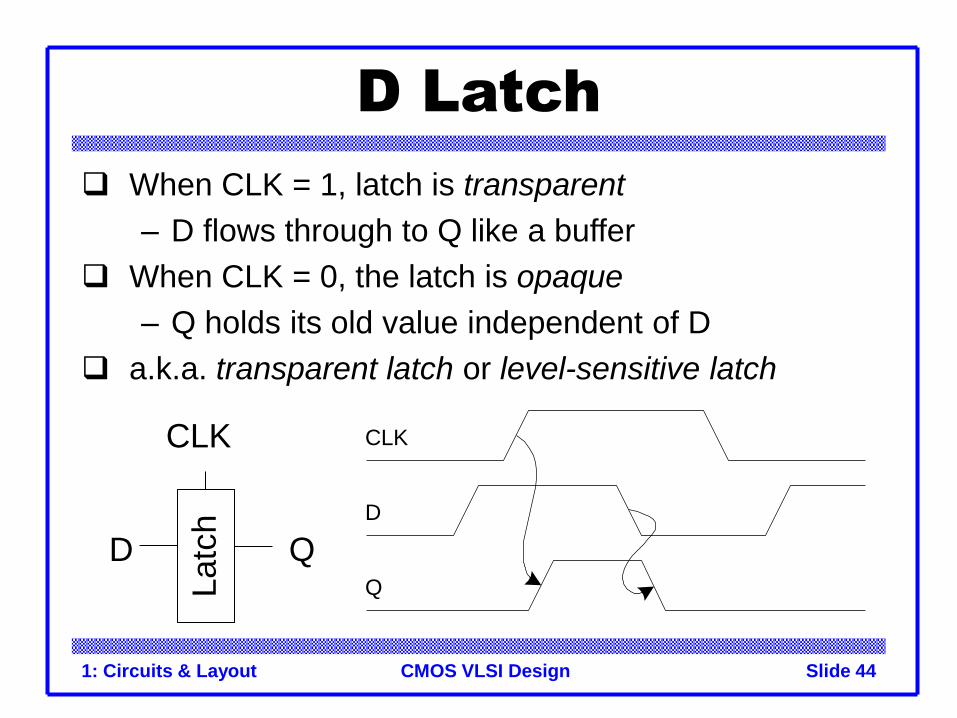
D Latch
When CLK = 1, latch is transparent
– D flows through to Q like a buffer
When CLK = 0, the latch is opaque
– Q holds its old value independent of D
a.k.a. transparent latch or level-sensitive latch
CLK
D Q
Latc
h D
CLK
Q
CMOS VLSI Design1: Circuits & Layout Slide 45
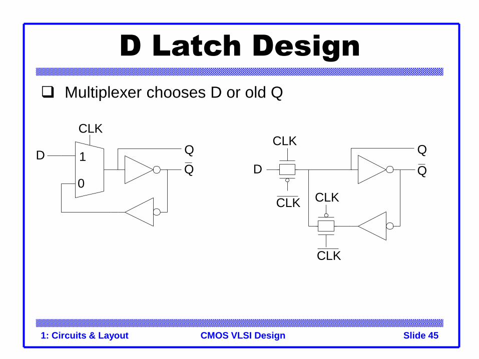
D Latch Design
Multiplexer chooses D or old Q
1
0
D
CLK
QCLK
CLKCLK
CLK
DQ Q
Q
CMOS VLSI Design1: Circuits & Layout Slide 46
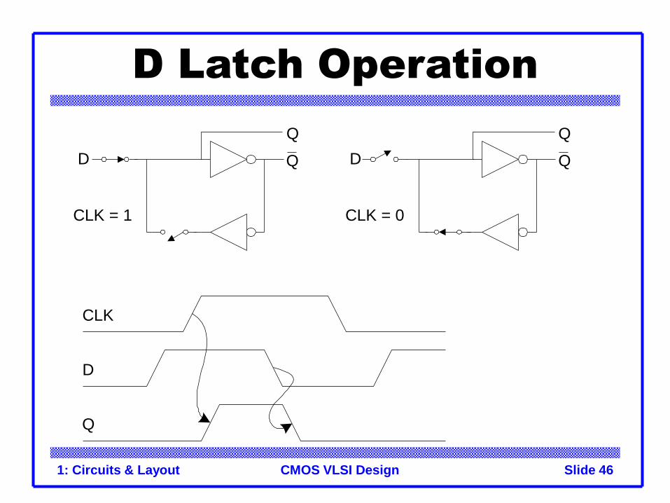
D Latch Operation
CLK = 1
D Q
Q
CLK = 0
D Q
Q
D
CLK
Q
CMOS VLSI Design1: Circuits & Layout Slide 47
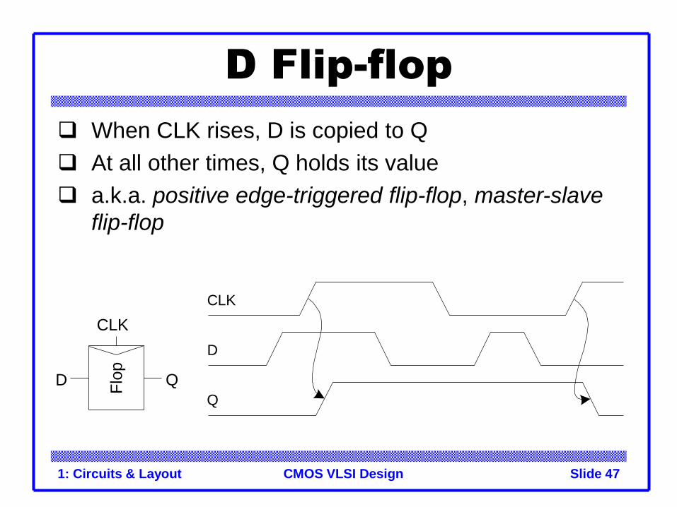
D Flip-flop
When CLK rises, D is copied to Q
At all other times, Q holds its value
a.k.a. positive edge-triggered flip-flop, master-slave
flip-flop
Flo
p
CLK
D Q
D
CLK
Q
CMOS VLSI Design1: Circuits & Layout Slide 48
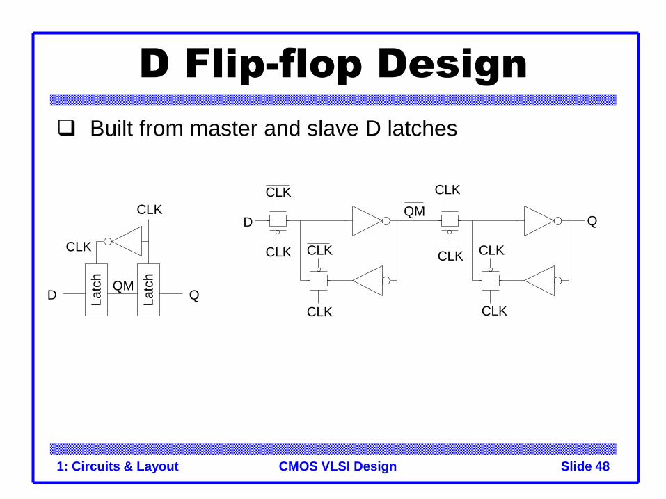
D Flip-flop Design
Built from master and slave D latches
QM
CLK
CLKCLK
CLK
Q
CLK
CLK
CLK
CLK
D
Latc
h
Latc
h
D QQM
CLK
CLK
CMOS VLSI Design1: Circuits & Layout Slide 49
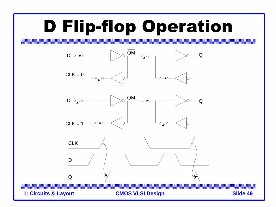
D Flip-flop Operation
CLK = 1
D
CLK = 0
Q
D
QM
QMQ
D
CLK
Q
CMOS VLSI Design1: Circuits & Layout Slide 50
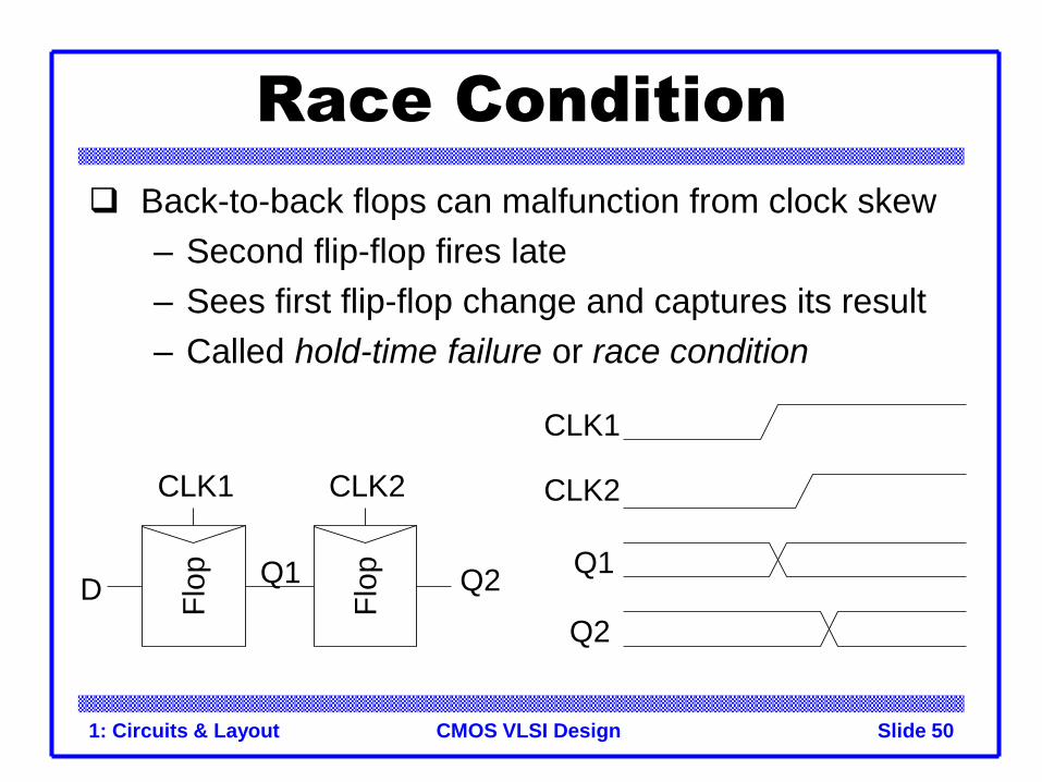
Race Condition
Back-to-back flops can malfunction from clock skew
– Second flip-flop fires late
– Sees first flip-flop change and captures its result
– Called hold-time failure or race condition
CLK1
DQ1
Flo
p
Flo
p
CLK2
Q2
CLK1
CLK2
Q1
Q2
CMOS VLSI Design1: Circuits & Layout Slide 51
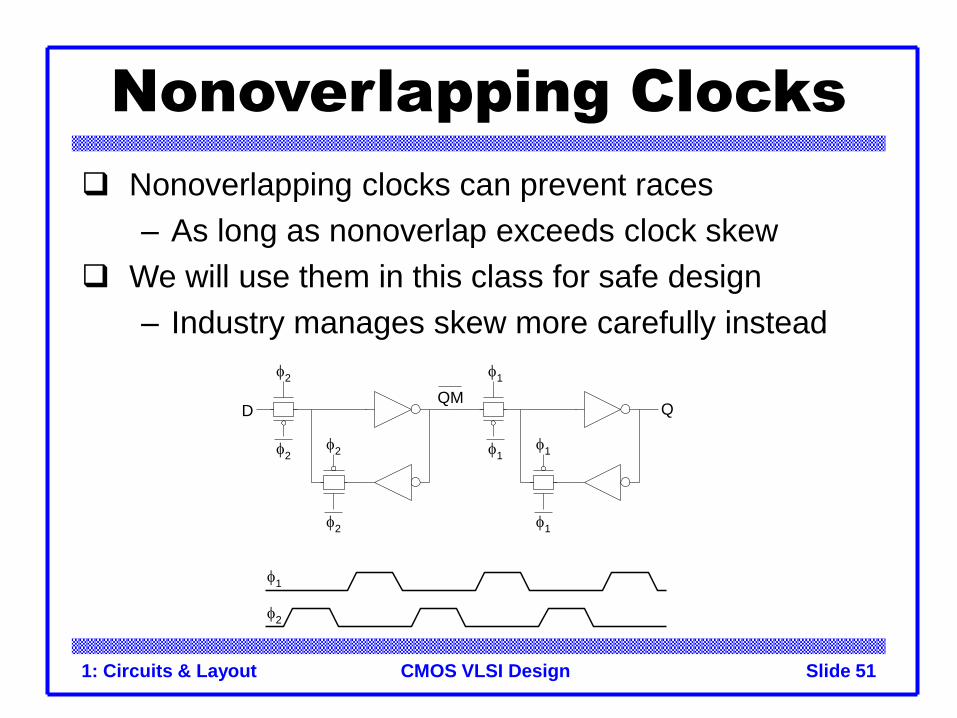
Nonoverlapping Clocks
Nonoverlapping clocks can prevent races
– As long as nonoverlap exceeds clock skew
We will use them in this class for safe design
– Industry manages skew more carefully instead
1
1
1
1
2
2
2
2
2
1
QMQD