Embed Size (px)
Citation preview

1
Learning Programming
with MyCo / TPS
Basically like playing Memory for Coders
Second Edition
now with more Features included. Chapters 0 to 8 are identical to the eBook version
Free Simulator for download
Online Simulator planned
Prepared to download Code into ARDUINO
ARDUINO Source Code included
Alternative: Forth Code for TI MSP430G2553
By Juergen Pintaske
A combined Project
and many People involved, mainly
Burkhard Kainka
Wilfried Klaas Michael Kalus
The first Kit is based on Holtek Chip, now Simulator Options and Arduino-based

2
This Book is Copyright © ExMark, 15 November 2018
The current Forth Bookshelf can be found at
https://www.amazon.co.uk/Juergen-Pintaske/e/B00N8HVEZM
All are available as eBook – the ones with P after the number as well as print book.
1 Charles Moore - Forth - The Early Years: Background information about the
beginnings of this Computer Language
2P Charles Moore - Programming A Problem Oriented Language: Forth - how the
internals work
3 Leo Brodie - Starting Forth -The Classic
4P Leo Wong – Juergen Pintaske – Stephen Pelc FORTH LITE TUTORIAL: Code
tested with free MPE VFX Forth, SwiftForth and Gforth or else
5P Juergen Pintaske – A START WITH FORTH - Bits to Bites Collection – 12 Words
to start, then 35 Words, Javascript Forth on the Web, more
6P Stephen Pelc - Programming Forth: Version July 2016
7P Brad Rodriguez - Moving Forth / TTL CPU / B.Y.O. Assembler
8 Tim Hentlass - Real Time Forth
9P Chen-Hanson Ting - Footsteps In An Empty Valley issue 3
10P Chen-Hanson Ting - Zen and the Forth Language: EFORTH for the
MSP430G2552 from Texas Instruments
11 Chen-Hanson Ting - eForth and Zen - 3rd Edition 2017: with 32-bit 86eForth
v5.2 for Visual Studio 2015
12P Chen-Hanson Ting - eForth Overview
13 Chen-Hanson Ting - FIG-Forth Manual Document /Test in 1802 IP
14 Chen-Hanson Ting - EP32 RISC Processor IP: Description and Implementation
into FPGA – ASIC tested by NASA
15 Chen-Hanson Ting – Irriducible Complexity
16P Chen-Hanson Ting - Arduino controlled by eForth
17 Burkhard Kainka - Learning Programming with MyCo: Learning Programming
easily - independent of a PC (Forth code to follow soon)
17bP Burkhard Kainka – Extended Version Programming with MyCo: Simulator
options - Arduino –source code, Tiny84 - Forth code MSP430G2553
18 Burkhard Kainka - BBC Micro:bit: Tests Tricks Secrets Code, Additional
MicroBit information when running the Mecrisp Package
19 Burkhard Kainka – Thomas Baum – Web Programming ATYTINY13
20P Georg Heinrichs – The ATTINY Project – Why Forth ?

3
Contents
0__Background 8
1__Introduction 10
2__Hardware tests 19
2.1_The basic structure 19
2.2_Two flashing LEDs 21
2.3_Counter combined with PWM 22
2.4_The Analog-to-Digital converter 28
2.5_Random number generator 30
2.6_Pulse length measurement 32
3__The programming mode 35
3.1_Reading out programs 35
3.2_Programming new functions 39
3.3_Back to factory status 42
4__MyCo instructions 43
4.1_The basic instructions 43
4.2_Calculations using Variables 48
4.3_Jumps and Skips 51
4.4_The instruction table 57
5__Program structures and sample programs 58
5.1_Counting loops 58
5.2_Compare instructions 60
5.3_Single bit processing 61
5.4_Basic logic functions 66
5.5_Subroutines 69
6__Advanced applications 72
6.1_Twilight switch 72
6.2_Two-point controller 73
6.3_LED dimmer 75
6.4_Morse code program 77
6.5_Start / Stop timer 80
6.6_Combination lock 82
7__The inner workings of MyCo 86
8__Appendix 89
8.1_Listings of sample programs 89
8.2_Instruction table 97
8.3_Programming model A, B, C 97

4
8.4_Circuit diagram 98
8.5_Function symbol 99
8.6_PCB with components 99
8.7_Header connectors SV1 and SV2 100
8.8_Hexadecimal table 101
8.9_Holtek processor block diagram 102
8.10_Breadboard 103
8.11_Resistor colors 103
8.12_Flow diagram symbols 104
8.13_Extension via PC Control Interface - Profilab 105
8.14_Circuit digram, Instruction Table 107
8.15_Programming pages 109
8.16_Links 111
8.17_MyCo_in_FORTH_MicroBox_Example 112
9.__Arduino Simulator and Interface to Arduino 113
9.1_The Simulator and first row of Buttons 115
9.2_The Function Window 116
9.3_Instruction Table 117
9.4_TPS/SPS Emulator 118
9.5_ ARDUINO GOES TPS 120
9.6_Instruction Tables 124
9.7_Download and ARDUINO Source Code 127
9.8_Holtek and Arduino version Instruction Tables 158
10.__TPS written in FORTH for TI MSP430G2553 160
11.__ATTINY 84 on solderless Breadboard 191
12.__Is Programming really that difficult? - Basics 193
4 Pages duplicated to be cut out as reference 201
Version MycoBook v26 print updated and extended 2018_11_15

5
A few first Words for this extended Version
First: There are some basic explanations in chapter 12, page 193 to get started.
Burkhard Kainka had a great idea: he defined a microcontroller kit, where a lot of the
complexity has been taken out, and all you need is the controller in the middle,
4 Inputs 2 analog Inputs 4 LED outputs
1 additional Output to simulate an analog output voltage.
All you need to program and control this little PLC ( Programmable Logic Controller )
unit are are 3 pushbuttons.
No PC required.
This first version is available from 3 sources as different setups:
from Franzis Verlag to learn programming and use the kit as a controller, but a lot
has happened since it appeared.
There is as well a kit you can buy from Conrad – no soldering required, built via a
solderless breadboard.
And the pre-programmed chip is abailable from AK-Modul.
Many people like this minimalistic approach, so many additional little applications
are available via Burkhard’s website.
An additional option was prepared by Wilfried Klass, where he made a Simulator
availabe, where you can program and execute the same functionality – but no kit
required.
But, seeing the real LED flash, or add the PLC to tou model train or model board
would be nice. Wilfried built this simulator for his own models – and for anybody
who is interested.
The next step, leading to this second edition, was his work to couple the Simulator
with external hardware and transfer the tested program. ARDUINO is the chosen
hardware, as there are probably 1 million or more out there already many probably
unused– so a nice target and no extra hardware required.
An additional option is then to take the chip out of the Arduino board, add what is
needed in your application around and stick a new chip into the Arduino board.
I am a big fan of the computer language Forth. It is not so well known, but follows
the minimalistic approach as well. There is a whole Forth Bookshelf for people who
are interested.
And it is interactive, so you can modify the program on the fly. Michael Kalus was
very kind and wote an emulator of the TPS/MyCo functionality in Forth. It runs on a
Texas Instrments MSP430G2553 chip and includes as well a serial interface function.

6
As result you can control the program on the chip either via the 3 buttons as before –
or from your PC and kann display a lot of the internal status. See Chapter 10.
And as last point in Chapter 11: PROGRAMMING. How difficult is it really? Well, you
do it every day without thinking about it.
I have chosen as first example a simplified making coffee using this controller and
instructions. Just try to extend this using the other instructions, it should not be too
difficult.
Oh, before I forget, in German the name is TPS; I could not find a good meaning for
these 3 letters in English, so I just calld it MyCo – my controller, as it will be in your
hand.
Enjoy reading. November 2018 version 21
Link to eBook – for now without extensions: https://www.amazon.co.uk/Learning-Programming-
MyCo-easily-independent-ebook/dp/B00K6N87UG/ref=asap_bc?ie=UTF8
Link to Franzis Kit - and downloadable part of English eBook http://www.elektronik-labor.de/Lernpakete/TPS/HandbuchTPS.htm
Link to Conrad Kit and documentation, many more examples
http://www.elektronik-labor.de/Lernpakete/TPS/TPS0.html
Link to AK-Modul
http://www.ak-modul-bus.de/stat/ht46f47e_mit_tps_firmware.html
Link to Forth Bookshelf https://www.amazon.co.uk/Juergen-Pintaske/e/B00N8HVEZM
Link to A Start With Forth data on Forth-ev.de
https://wiki.forth-ev.de/doku.php/en:projects:a-start-with-forth:start0
Link to Burkhard Kainka’s website and TPS for ATMEGA8
https://wiki.forth-ev.de/doku.php/en:projects:a-start-with-forth:start0 And Most Important: Link to the Wilfried Klaas website regarding TPS http://wkla.no-ip.biz/ArduinoWiki/doku.php?id=arduino:arduinosps:spsemu

7
9.1 The Simulator and the Row of Buttons |-- EXIT the program
| |-- CREATE a NEW program ( Control+N )
| | |-- OPEN a file ( Control+O )
| | | |-- SAVE the actual program ( Control + S )
| | | | |-- ADD a new line to the program
| | | | | |-- DELETE the actual line
| | | | | | |-- SHOW the actual programming file
| | | | | | | |-- UPLOAD the program to the target ( Control+U )
| | | | | | | | |-- CREATE a HEX file
| | | | | | | | | |-- EXECUTE a single instruction ( F5 )
| | | | | | | | | | |-- Execute the next step ( F8 )
| | | | | | | | | | | |-- STOP the debug program execution ( F6 )
| | | | | | | | | | | | | -- START / STOP program execution ( F9)
| | | | | | | | | | | | | |-SELECT target Holtek-Mega8-TINY84-Arduino
Memory: Showing the memory locations where the instructions are stored
Instruction: Instruction to be executed at the memory execution
Data: Data related to the instruction
Description: Automatically added description
Comment: Own comment to be added
Instruction: Instruction to be inserted into the current memory location
Data: Then open Data and select related number or function

8
9.2 - The Function Window - on the right hand side
PRG / Program SEL / Select INPUTS:
Input 1 – 4 The four inputs to be set by mouse click
ADC 1, 2 Two simulated analog inputs – input a number between 0 … 255
RC1, 2 Two simulated RC servo outputs – input a number between 0 … 255
OUTPUTS:
Output 1 – 4 The four output bits sent by the PLC – Programmable Logic Controller
PWM 1, 2 Pulse Width Modulated outputs, an ON / OFF rectangular output signal
Servo 1, 2 RC servo outputs, simulating the angle by showing a number plus icon Tone: A sound to be output – to be added later
INTERNAL DATA of this PLC: The inputs are fed via the instructions into registers
RA, RB, RC, RD, ( RE, RF ) and processed
Addr The current memory location addressed
Page Each memory block page consists of 16 locations, the page display changes accordingly
And JUMPs will setting up a PAGE number if different
Radr RETURN ADDRESS – if subroutine is called, return address is shown here
DELAY Showing time is a delay instruction is executed ( SKIP If a skip decision is executed, 1 indicates jump over next instruction ) tbd

9
9.3 - Instruction Table Instruction Set shaded in yellow aextensions of ArduinoSPS/ATTiny84 version.
0 1 2 3 4 5 6 7
n.n. Port Delay Jump back rel
A= „=A“ A= A= Options
0 NOP off 1ms 0 0 A<->B
1 1 2ms 1 1 B=A A=B A=A + 1
2 2 5ms 2 2 C=A A=C A=A - 1
3 3 10ms 3 3 D=A A=D A=A + B
4 4 20ms 4 4 Dout=A Din A=A - B
5 5 50ms 5 5 Dout.0=A.0 Din.0 A=A * B
6 6 100ms 6 6 Dout.1=A.0 Din.1 A=A / B
7 7 200ms 7 7 Dout.2=A.0 Din.2 A=A and B
8 8 500ms 8 8 Dout.3=A.0 Din.3 A=A or B
9 9 1s 9 9 PWM.0=A ADC.0 A=A xor B
a 10 2s 10 10 PWM.1=A ADC.1 A= not A
b 11 5s 11 11 Servo.0=A RCin.0 A= A % B (Rem.)
c 12 10s 12 12 Servo.1=A RCin.1 A= A + 16 * B
d 13 20s 13 13 E=A A=E A= B - A
e 14 30s 14 14 F=A A=F
f 15 60s 15 15 Push A Pop A
8 9 a b c d e f
Page Jump
absolute
C* D* Skip if Call # +
(16* Page)
Callsub
/Ret
Byte Instr.
0 0 0 0 A=0 0 ret A=ADC.0
1 1 1 1 A>B 1 Call 1 A=ADC.1
2 2 2 2 A<B 2 2 A=RCin.0
3 3 3 3 A=B 3 3 A=RCin.1
4 4 4 4 Din.0=1 4 4 PWM.0=A
5 5 5 5 Din.1=1 5 5 PWM.1=A
6 6 6 6 Din.2=1 6 6 Servo.0=A
7 7 7 7 Din.3=1 7 Servo.1=A
8 8 8 8 Din.0=0 8 Def 1
9 9 9 9 Din.1=0 9 2
10 10 10 10 Din.2=0 10 3
11 11 11 11 Din.3=0 11 4
12 12 12 12 S_PRG=0 12 5
13 13 13 13 S_SEL=0 13 6
14 14 14 14 S_PRG=1 14
15 15 15 15 S_SEL=1 15 restart PrgEnd

10
9.4 - TPS / SPS Emulator http://wkla.no-ip.biz/ArduinoWiki/doku.php?id=arduino:arduinosps:spsemu
Switch top left to English if needed. Copied from Willie’s website
For the TPS PLC (and my extensions) I once wrote an emulator as a fun project.
Here the result.
The complete project is programmed in Lazarus (Freepascal).
The emulator can work with the different instruction sets of different TPS versions.
On the left you can see the programming window.
This can either be typed in directly or generated via the two combo boxes below.
There you can select the possible commands – dependent on the target selected of
the included versions.
The commands can then be executed via the 4 buttons in the top center block.
The first button tests the currently selected command (jumps are not carried out)
The second button executes the program in single-step mode.
The third button stops single-step mode
The fourth button is Start-Stop, to run at maximum speed.
In the left window you make the entries and view the results as you step through the
program.

11
At the bottom you can see a few more the drop downs with the instructions.
.
On the right you can set inputs and see results at the outputs.
The lower block on the right shows what is happening internally in the simulated
processor.
And additional documentation in English will be made available.
ATTENTION: The current version of Avira Antivirus has a false positive message.

12
9.6 - Instruction Set Areas shaded in yellow are extensions of my ArduinoSPS and ATTiny84 version.
0 1 2 3 4 5 6 7
n.n. Port Delay Jump back relative
A= „=A“ A= A= Options
0 NOP off 1ms 0 0 A<->B
1 1 2ms 1 1 B=A A=B A=A + 1
2 2 5ms 2 2 C=A A=C A=A - 1
3 3 10ms 3 3 D=A A=D A=A + B
4 4 20ms 4 4 Dout=A Din A=A - B
5 5 50ms 5 5 Dout.0=A.0 Din.0 A=A * B
6 6 100ms 6 6 Dout.1=A.0 Din.1 A=A / B
7 7 200ms 7 7 Dout.2=A.0 Din.2 A=A and B
8 8 500ms 8 8 Dout.3=A.0 Din.3 A=A or B
9 9 1s 9 9 PWM.0=A ADC.0 A=A xor B
a 10 2s 10 10 PWM.1=A ADC.1 A= not A
b 11 5s 11 11 Servo.0=A RCin.0 A= A % B (Rem.)
c 12 10s 12 12 Servo.1=A RCin.1 A= A + 16 * B
d 13 20s 13 13 E=A A=E A= B - A
e 14 30s 14 14 F=A A=F
f 15 60s 15 15 Push A Pop A
Additional Features of the ArduinoSPS version:
There are 2 additional registers (E and F)
And there is a stack area with the 2 usual interface methods push ( add to stack)
and pop (take off the stack). There are 16 level positions in this stack.
There are also 2 new calculations; one is the remainder of a division (A = A% B)
and one an 8-bit conversion. A = A + 16 * B
Since version 0.6, the swap command has also been added, swapping the A and B
register contents.
And a new calculation A = B - A. Especially, when you are working in an 8- bit
space, it is sometimes quite cumbersome to carry out such an operation without.

13
8 9 a b c d e f
Page Jump
absolute
(#+
16*page)
C* C>0:
C=C-1;
# + (16*
page)
D*D>
0: D=D-
1;
# + (16*
page)
Skip if Call # +
(16*
Page)
Callsub
/Ret
Byte Instr.
0 0 0 0 A=0 0 ret A=ADC.0
1 1 1 1 A>B 1 Call 1 A=ADC.1
2 2 2 2 A<B 2 2 A=RCin.0
3 3 3 3 A=B 3 3 A=RCin.1
4 4 4 4 Din.0=1 4 4 PWM.0=A
5 5 5 5 Din.1=1 5 5 PWM.1=A
6 6 6 6 Din.2=1 6 6 Servo.0=A
7 7 7 7 Din.3=1 7 Servo.1=A
8 8 8 8 Din.0=0 8 Def 1
9 9 9 9 Din.1=0 9 2
10 10 10 10 Din.2=0 10 3
11 11 11 11 Din.3=0 11 4
12 12 12 12 S_PRG=0 12 5
13 13 13 13 S_SEL=0 13 6
14 14 14 14 S_PRG=1 14
15 15 15 15 S_SEL=1 15 restart PrgEnd
Aditional Features in this ArduinoSPS version:
As we now have more EEPROM memory, the page area is been extended to 16
pages. So, you can now enter a program that is 256 bytes long.
Regarding the Skip command, there is now as well the Skip command for
condition A = 0.
Via the E commands, you can now program 6 real subroutines. These are created
using the Def# command. With Call# the routine is started. With Return you come
back to the main program. The Def# may also be positioned above the 256 bytes in
the EEPROM. So, also outside the range of the jump commands.
Also new is the Restart command, which restarts the entire controller.
In the F area, there are the new commands located, which work with the extended
8-bit resolution.
FF means end of program. → and an automatic jump to program location 00.

14
And now please have fun with the ArduinoSPS.
Oh, and as always: everything without any warranty ...
And here the picture of a small test setup:

15
9.8 - TPS/MyCo-A 4-Bit SPS to learn Programming
in SW or using HOLTEK http://wk-music.de/ArduinoWiki/ Part 1
0 1 2 3 4 5 6 7
n.n. Port
Delay Ju <- rel A= „=A“ A= A=Calculations
0 NOP 0 1ms 0 0 A<->B
1 1 2ms 1 1 B=A A=B A=A + 1
2 2 5ms 2 2 C=A A=C A=A - 1
3 3 10ms 3 3 D=A A=D A=A + B
4 4 20ms 4 4 Dout=A Din A=A - B
5 5 50ms 5 5 Dout.0=A.0 Din.0 A=A * B
6 6 100ms 6 6 Dout.1=A.0 Din.1 A=A / B
7 7 200ms 7 7 Dout.2=A.0 Din.2 A=A AND B
8 8 500ms 8 8 Dout.3=A.0 Din.3 A=A OR B
9 9 1s 9 9 PWM.0=A ADC.0 A=A XOR B
A 10 2s 10 10 ADC.1 A= NOT A
B 11 5s 11 11
C 12 10s 12 12
D 13 20s 13 13
E 14 30s 14 14
F 15 60s 15 15
And Part 2
8 9 A B C D E F
Page JMP C* D* Skip if Ca RET . SPS
0 0 0 0 0 0 3 2 1 0
1 1 1 1 A>B 1 1 INPUT
2 2 2 2 A<B 2 2 Reg A
3 3 3 3 A=B 3 3 Reg B
4 4 4 4 Din.0=1 4 4 ALU
5 5 5 5 Din.1=1 5 5 Reg C
6 6 6 6 Din.2=1 6 6 Reg D
7 7 7 7 Din.3=1 7 7
8 8 8 Din.0=0 8 8
9 9 9 Din.1=0 9 9 OUT
10 10 10 Din.2=0 10 A PagReg
11 11 11 Din.3=0 11 B ProCtr
12 12 12 S_PRG=0 12 C Delay
13 13 13 S_SEL=0 13 D Skip
14 14 14 S_PRG=1 14 E
15 15 15 S_SEL=1 15 F FF 3 2 1 0

16
TPS / MyCo - A 4-Bit SPS to learn Programming – in SW only
or running on Arduino http://wk-music.de/ArduinoWiki/
0 1 2 3 4 5 6 7
n.n. Port Delay Ju <- rel A= „=A“ A= A=Calculations
0 NOP 0 1ms 0 0 A<->B
1 1 2ms 1 1 B=A A=B A=A + 1
2 2 5ms 2 2 C=A A=C A=A - 1
3 3 10ms 3 3 D=A A=D A=A + B
4 4 20ms 4 4 Dout=A Din A=A - B
5 5 50ms 5 5 Dout.0=A.0 Din.0 A=A * B
6 6 100ms 6 6 Dout.1=A.0 Din.1 A=A / B
7 7 200ms 7 7 Dout.2=A.0 Din.2 A=A AND B
8 8 500ms 8 8 Dout.3=A.0 Din.3 A=A OR B
9 9 1s 9 9 PWM.0=A ADC.0 A=A XOR B
A 10 2s 10 10 PWM.1=A ADC.1 A= NOT A
B 11 5s 11 11 Servo.0=A RCin.0 A= A % B (Rest)
C 12 10s 12 12 Servo.1=A RCin.1 A= A + 16 * B
D 13 20s 13 13 E=A A=E A= B - A
E 14 30s 14 14 F=A A=F
F 15 60s 15 15 Push A Pop A
X9 Jump absolut (#+16*page), X10 C* C>0: C=C-1; # + (16*page) X11 D*D>0:D=D-1; # + (16*page) XD Call # + (16*Page)
8 9 A B C D E F
Page X9 X10 X11 Skip if Call /Ret Byte Instr. SPS
0 0 0 0 A=0 0 Ret A=ADC.0 3 2 1 0
1 1 1 1 A>B 1 Call1 A=ADC.1 INPUT
2 2 2 2 A<B 2 Call2 A=RCin.0 Reg A
3 3 3 3 A=B 3 Call3 A=RCin.1 Reg B
4 4 4 4 Din.0=1 4 Call4 PWM.0=A ALU
5 5 5 5 Din.1=1 5 Call5 PWM.1=A Reg C
6 6 6 6 Din.2=1 6 Call6 Servo.0=A Reg D
7 7 7 7 Din.3=1 7 Servo.1=A Reg E
8 8 8 8 Din.0=0 8 Def1 Reg F
9 9 9 9 Din.1=0 9 Def2 OUT
10 10 10 10 Din.2=0 10 Def3 PageReg
11 11 11 11 Din.3=0 11 Def4 Prog.Ctr
12 12 12 12 S_PRG=0 12 Def5 Delay
13 13 13 13 S_SEL=0 13 Def6 Skip
14 14 14 14 S_PRG=1 14
15 15 15 15 S_SEL=1 15 Restart PrgEnd 3 2 1 0

17
10 - TPS / MyCo written in Forth
As you might have seen in one of the first pages, most of the books I publish are
related to the language FORTH.
When the first version was written, I just got into Forth again after a long time.
I got great help from Michael Kalus, who could be convinced to emulate Burkhard
Kainka’s TPS in Forth, written for the TI MSP430 in a 20-pin package.
This then led to the MicroBox, a small board plus the option of a header board –
which as you can see now, exactly has the 3 switches and 4LEDs plus one for PWM
output.
All of the TPS functions can be replicated, but here you actually have a complete
FORTH Interpreter/Compiler ON the chip as well. There is a command to exit the
“local” function control of the 3 switches to the serial terminal function.
The extension of this book adds the opportunity to include the Forth code now, so
people can give it a go and understand Forth code.
A good starting point would be to look at the documetation at
http://wiki.forth-ev.de/doku.php/en:projects:a-start-with-forth:start
For the eBook / Print Book, see the Forth Bookshelf at
https://www.amazon.co.uk/Juergen-Pintaske/e/B00N8HVEZM
Here the code that had been running on these boards.
To Flash the initial program into the chip needs the TI Launchpad connected to the
PC. Afterwards the chip is independent just needing a USBtoSERIAL – or if just used
as controller with the TPS Interface and nothing else is needed.
See pictures on page 118.
\ MyCo \ using 4e4th Release0.34b
\ Version 0.91 - edit pages using only S2 and S1.
\ started: 2014_08_10 now 2015_03_28
\ Achtung:
\ Zweistellige Ziffern sind Kommandos in MYCO !!
\ Willst du Zahlen eingeben, müssen Nullen davor sein.
\ Beispiel:
\ 59 lädt Register A in das PWM-Register.

18
\ 0059 legt den Zahlenwert 59 auf den Datenstack.
\ Careful:
\ Two-digit numbers are commands in MYCO !!
\ If you want to enter numbers, zeros must be in front of them.
\ Example:
\ 59 loads register A into the PWM register.
\ 0059 places the number 59 on the data stack.
\ Issues:
\ WIPE strikes after EDIT ; fixed 24.02.2015
\ ugly EDIT; made a better one; 12.10.2014
\ S1 and S2 input faild sometimes; fixed 12.10.2014
\ STEP does wrong dumping; fixed 08.10.2014
\ +++++++++++++++++++++++++++++++++++++++++++++++++++++++++++++
\
\ Start of the Program MyCo, programmed in Forth
\ Based on Burkard Kainka's TPS, Juergen Pintaske
\ translated the German Manual into English and extended it.
\ This program in Forth simulates a very small processor, running
\ in a Franzis Kit which is planned to help Learning Programming;
\ and we use it here as an example of how to program the TI
\ MSP430 Controller. Owners of this Franzis kit can just add a
\ programmed MSP430G2553 and a reset resistor and replace the Holtek.
\ And all three options can be used to learn:
\ First, use the original TPS, running on a Holtek Processor,
\ and with the Hardware available from Franzis or Conrad.
\ Second, use the existing Hardware, take the Holtek chip out
\ and add a little board with the MSP430 Controller on it.
\ Just jumper the necessary wires to the preprogrammed MSP430.
\ Third, get a programmed MSP430 controller, add the 5 resistor LED
\ combinations and the 3 switches to 430 board,
\ and run completely in the MSP430,
\ but in addition
\ now with aserial
\ terminal control, showing on screen what actually happens
\ internally in all of the simulated processor registers.
\ This all looks like an overkill, but the target is here:
\ Learn Programming in a language called Forth
\ - so as an Application.

19
\ A Note when using the serial terminal function:
\ Use the hex numbers only with preceding zeros.
\ Any hex XX without a proceeding 0 is interpreted as a command.
\ Example:
\ 71 is the command A<=A+1, 0071 is interpreted as a number.
\ Defining the I/O for this application
\ Device Pinout: MSP430G2553 20-Pin PDIP
\ (TOP VIEW)
\ VCC----+3.3V--------[01 20]--Ground-----------VSS
\ (LED1 LP) AD1 P1.0--[02 19]--P2.6 OUT2 – 470R + LED to GND
\ RXD-----------P1.1--[03 18]--P2.7 OUT3 – 470R + LED to GND
\ TXD-----------P1.2--[04 17]--test
\ S2 to GND P1.3--[05 16]--RST S1-LP to GND
\ ..........AD2 P1.4--[06 15]--P1.7 S1 to GND
\ _-_-_-_-_-FRQ P1.5--[07 14]--P1.6 PWM – 470R + LED to GND
\ ----------IN0 P2.0--[08 13]--P2.5 OUT1 – 470R + LED to GND
\ ----------IN1 P2.1--[09 12]--P2.4 OUT0 – 470R + LED to GND
\ ----------IN2 P2.2--[10 11]--P2.3 IN3
\ LP = TI Launchpad
\
\ P1.0 used as Input, later on as Analog Input 1
\ P1.1 RX and
\ P1.2 TX are used as the serial interface to the PC,
\ mostly via USBtoTTL
\ P1.3 used as S2, as on the TI Launchpad,
\ the internal resistor is enabled
\ P1.4 used as Input, later on as Analog Input 2
\ P1.5 used as Output, later on to output a frequency
\ with defined length
\ P1.6 Output, later on as Pulse Width Modulation output
\ - quasi D/A Output
\ resistor about 470 Ohms and LED to Ground
\ P1.7 Input S1, internal resistor enabled
\ P2.0 Input 0 internal resistor enabled, so open input means HIGH
\ P2.1 Input 1 internal resistor enabled, so open input means HIGH
\ P2.2 Input 2 internal resistor enabled, so open input means HIGH
\ P2.3 Input 3 internal resistor enabled, so open input means HIGH
\ P2.4 Output 0 resistor about 470 Ohms and LED to Ground

20
\ P2.5 Output 1 resistor about 470 Ohms and LED to Ground
\ P2.6 Output 2 resistor about 470 Ohms and LED to Ground
\ P2.7 Output 3 resistor about 470 Ohms and LED to Ground
\ One of the important issues to be solved here
\ was to use the FLASH memory of the MSP430 as an
\ EEPROM functionality needed for local programming,
\ this is an internal issue for later and can be skipped for now
\ The original Holtek Controller has 128 Bytes of EEPROM
\ 'EEROM' simulaton in flash memory -- see the chapter further down
\ The Programming Model of this Minimum Processor
\ is simulated in Forth.
\ Remember: for simplicity this processor is used
\ as 4 bit, everything is in nibbles.
\ This is about the same processor
\ as in Burkhard Kainka's original design:
\ PC Program Counter limited to address memory locations 0 - 127,
\ 00 to 7F in HEX
\ PG Page register 4 bit, combined with the 4 bit jump address
\ achieves the 256 ($100)
\ DL Delay register, a delay from 1ms to 60 sec can be programmed.
\ SK Skip register indicates a possible skip over instructions
\ based on comparisons
\ There are no conditional branches
\ - just these Conditional Skips for simplicity
\ Easy for beginners as the program code is relocatable
\ (address independent)
\ The main processor registers and other registers:
\ IN 4 bit input, when used reflects the status of the 4 Input lines
\ A 4 bit A register, somehow the central register,
\ the ALU works with A register
\ B 4 bit B register
\ C 4 bit C register
\ D 4 bit D register
\ A1 4 bit Analog Input Channel 1
\ A2 4 bit Analog Input Channel 2
\ PW 4 bit Pulse Width Modulated Output, can used filtered
\ as quasi analog output

21
\ OU 4 bit output register, 4 Output Pins will reflect
\ the contents, LEDS display it
\ There are two options to program the program
\ for this simulated processor:
\ via the switches (and needes setting the IN bits
\ for page selection), or
\ control completely via the serial interface
\ - mostly to a PC, after enter q
\ so a more complex part of this program is used to
\ show the processor status
\ on the monitor
\ Display all of the variables in this processor,
\ here formatted differently
\ PC PG DL SK IN A B C D A1 A2 PW OU
\ x x x x x x x x x x x x x x
\ The next part of thei program is related to showing
\ how the FLASH Memory is used
\ as simulated EEPROM, so skip over this for now.
\ *** Let us start with an empty user flash ***
HEX \ Just set for terminal IO and display,
\ the options are HEX and DECIMAL
\ membot 0000 + constant seg0 ; this did not work, see issues.
\ membot 0200 + constant seg1
\ PAD constant CACHE \ PAD is already there in forth,
\ so we use it. Commented out here
1000 constant EE0 \ start address of info-d
1040 constant EE1 \ start address of info-c
0040 constant SEGSIZ \ segment size
0010 constant BLKSIZ \ bytes in block (alias "page" of MyCo)
variable SEG \ holding segment number in use
variable BLK \ holding block number
variable UPD \ this variable shows if the cache has been updated

22
\ As we are simulating an existing system,
\ we use the same TPS example programs
\ 128 bytes of example programms = 8 pages -- page0 .. page7
HEX
IHERE
\ Page0
64 ic, 51 ic, 4E ic, 80 ic,
C3 ic, 98 ic, 82 ic, 95 ic,
4D ic, 80 ic, C3 ic, 9E ic,
82 ic, 9A ic, 4B ic, 81 ic,
\ Page1
C3 ic, 94 ic, 83 ic, 90 ic,
47 ic, 81 ic, C3 ic, 9A ic,
83 ic, 94 ic, 43 ic, 82 ic,
C3 ic, 90 ic, 84 ic, 90 ic,
\ Page2
11 ic, 28 ic, 18 ic, 28 ic,
34 ic, 71 ic, 54 ic, 59 ic,
26 ic, 34 ic, 69 ic, 54 ic,
59 ic, 26 ic, 34 ic, FF ic,
\ Page3
54 ic, CE ic, 71 ic, 33 ic,
22 ic, CC ic, 32 ic, 40 ic,
22 ic, 71 ic, 54 ic, CE ic,
34 ic, 39 ic, FF ic, FF ic,
\ Page4
86 ic, D0 ic, 40 ic, 71 ic,
54 ic, 23 ic, CD ic, 34 ic,
D8 ic, 40 ic, 54 ic, 3B ic,
FF ic, FF ic, FF ic, FF ic,
\ Page5
4F ic, 93 ic, 45 ic, 53 ic,
19 ic, 11 ic, 21 ic, 19 ic,
11 ic, 21 ic, 19 ic, 11 ic,
20 ic, B4 ic, 10 ic, E0 ic,
\ Page6
23 ic, CE ic, 32 ic, 23 ic,
CC ic, 31 ic, E0 ic, FF ic,
23 ic, CF ic, 32 ic, 23 ic,
CD ic, 31 ic, E0 ic, FF ic,
\ Page7
CC ic, 31 ic, 40 ic, 54 ic,

23
23 ic, CE ic, 32 ic, CF ic,
E0 ic, CC ic, 33 ic, 71 ic,
23 ic, CC ic, 31 ic, 3C ic,
ihere
constant EXEND
constant EX0
\ Now the real activity starts: The default programs above
\ are copied into the
\ 128 bytes of Program Area available for programming
\ and will show some demos,
\ using this code \ after a Reset.
HEX
: PRG0 \ -- \ copy the default progams to the
\ simulated 'eeprom' area in FLASH
ee0 segsiz flerase
ee1 segsiz flerase
ex0 ee0 exend ex0 - d->i ;
\ The memory of the MSP430 will be rather fully used.
\ So, to save Program Space,
\ the 4 Bit Nibbles are packaged into 4 nibbles
\ to be one Variable of 16 bits.
\ This will save on RAM used, and is as well a programming exercise.
\ Juggling nibbles mk0 (this shows how extensively
the code has been tested)
HEX
: 0! \ n adr -- \ store nibble 0 to value at address
>r r@ @ FFF0 and swap F and + r> ! ;
: 1! \ n adr -- \ store nibble 1 to value at address
>r r@ @ FF0F and swap F and 4 lshift + r> ! ;
: 2! \ n adr -- \ store nibble 2 to value at address
>r r@ @ F0FF and swap F and 8 lshift + r> ! ;
: 3! \ n adr -- \ store nibble 3 to value at address
>r r@ @ 0FFF and swap F and C lshift + r> ! ;

24
: 0@ \ adr - n \ fetch nibble 0 of value at address
@ 000F and ;
: 1@ \ adr - n \ fetch nibble 1 of value at address
@ 00F0 and 0004 rshift ;
: 2@ \ adr - n \ fetch nibble 2 of value at address
@ 0F00 and 0008 rshift ;
: 3@ \ adr - n \ fetch nibble 3 of value at address
@ F000 and 000C rshift ;
\ As a first step, we have to define and program the relevant IO Bits
\ of the chip as Input (with enabling internal pull-up resistor)
\ or as Output.
\ In this part of the program you can find the relevant memory mapped
\ addresses to
\ Set the IO functionality,
\ Read Input Data,
\ Write Output Data
\ Some of the possible internal MSP430 functions are rather complex,
\ so here
\ IO Bits are used as simple Input / Output only,
\ additional Forth Code later
HEX
: INITIO \ -- \ I/O initialisation of MyCo ports mk0
\ mask adr op
\ 76543210
[ bin ] 10011001 [ hex ] 0022 ( P1DIR ) cclr \ P1 INs
[ bin ] 01100110 [ hex ] 0022 ( P1DIR ) cset \ P1 OUTs
[ bin ] 10001000 [ hex ] 0024 ( P1IES ) cset \ falling edge detect
[ bin ] 00100000 [ hex ] 0026 ( P1SEL ) cset \ P1.5 sec func
\ TA0.0 (FRQ)
[ bin ] 10001000 [ hex ] 0027 ( P1REN ) cset \ pullup selected
[ bin ] 10000000 [ hex ] P1 cset \ P1.7 pullup enabled
[ bin ] 00001111 [ hex ] 002A ( P2DIR ) cclr \ P2 INs
[ bin ] 11110000 [ hex ] 002A ( P2DIR ) cset \ P2 OUTs
[ bin ] 00001111 [ hex ] 002F ( P2REN ) cset \ P2 pullups selected
[ bin ] 00001111 [ hex ] P2 cset \ P2 pullups enabled

25
[ bin ] 11000000 [ hex ] 002E ( P2SEL ) cclr \ clear these bits
\ to I/O
; \ end of IO Setting Definition Word
INITIO \ now execute the word INITIO
HEX \ Set to HEX for some basic peripheral operations
: OUT! \ n -- \ write to output pins (nibble, 0004 LEDs)
\ do NOT use c! word - this would reset the pull-ups!
F0 p2 cclr 000F and 0004 lshift p2 cset ;
023 constant P1IFG \ define a constant P1IFG
: S1? 080 P1IFG cget ; \ -- f \ set on edge event.
: S1- 080 P1IFG cclr ; \ -- \ reset flag
: S2? 008 P1IFG cget ; \ -- f \ set on edge event.
: S2- 008 P1IFG cclr ; \ -- \ reset flag
: IN@ \ -- n \ read digital input pins (nibble )
P2 1- c@ 000F and ;
\ Now we are ready to define the simulated processor;
\ As explained before, the Registers are packed into 16 bit variables
\ SGPC PDSI ABCD 12WO
\ xxxx xxxx xxxx xxxx
HEX
variable SGPC \ Segment(4 bit), PageCounter(4 bit)
\ and PC (2x 4 bit)
variable RTRN \ ReTuRN address (copy of the SGPC before call happens)
variable PDSI \ Page_Preset, Delay, Skip, Input
variable ABCD \ registers A B C D
variable 12WO \ ad1, ad2, pWm, out

26
\ LED display operations
: OUT> ( -- n ) 12wo 0@ ; \ pull OUT nibble onto stack
: >OUT ( n -- ) 12wo 0! ; \ push n to OUT nibble
: OUT. \ n -- \ \ display n at OUT-LEDs,
\ copy n to OUT-register
dup out! >out ;
: ? ( adr -- ) c@ . ; \ define a Word to show the byte
\ ( 8 bits) at an address
: ?? ( adr -- ) @ u. ; \ define a Word to show a cell
\ (16 bits) at address unsigned
\ Now we have to define the instructions
\ that this processor can execute
\ Define Instructions:
\ The first group of Instructions covers 0n –
\ n has the values of 00 to 0F
\ Tones are output by the MSP430G2553, 8Mhz DCO and SMCLK /2

27
HEX
\ 0n - set tone pitch n
\ output a square wave at P1.5 (pin 7) mk0
: P15SEC 020 dup p1 1+ cset 026 cset ; \ set P1.5 using TA0.0
: P15IO 020 026 cclr 020 041 cclr ; \ set p1.5 as GPIO
: TON- zero 0160 ! p15io ; \ stop timer
: TON+ \ n -- \ start timer-A with interval n
p15sec \ init pin
0080 0162 ! \ CCTL0 set timer output mode
( n ) 0172 ! \ CCR0 set interval
0254 0160 ! \ CTL start timer clock, mode and divider
;
\ --> intermediate-stage-0.txt
\ up to here can be programmed using the intermediate-stage-0.txt file
DECIMAL \ MIDI Tones B3 to B5, 2 Octaves; pitch list. mk0
: 00 ton- ;
: 01 7962 ton+ ; \ B3
: 02 7515 ton+ ; \ C4
: 03 6695 ton+ ; \ D4
: 04 5965 ton+ ; \ E4
: 05 5630 ton+ ; \ F4
: 06 5016 ton+ ; \ G4
: 07 4469 ton+ ; \ A4
: 08 3981 ton+ ; \ B4
: 09 3758 ton+ ; \ C5
: 0A 3348 ton+ ; \ D5
: 0B 2983 ton+ ; \ E5
: 0C 2815 ton+ ; \ F5
: 0D 2508 ton+ ; \ G5
: 0E 2235 ton+ ; \ A5
: 0F 1991 ton+ ; \ B5
\ The next group of Instructions covers 1n - 10 to 1F,

28
\ just stores a hex number into the Output register,
\ no other register affected
\ 1n - Load Out with number n \ mk1
HEX
: 10 0000 out. ;
: 11 0001 out. ;
: 12 0002 out. ;
: 13 0003 out. ;
: 14 0004 out. ;
: 15 0005 out. ;
: 16 0006 out. ;
: 17 0007 out. ;
: 18 0008 out. ;
: 19 0009 out. ;
: 1A 000A out. ;
: 1B 000B out. ;
: 1C 000C out. ;
: 1D 000D out. ;
: 1E 000E out. ;
: 1F 000F out. ;
\ 2n - Load the Delay Register with a number from 0–F mk1
DECIMAL
: DLY ( n -- ) PDSI 2! ;
: SEC ( n -- ) 0000 DO 1000 ms LOOP ;
: 20 0000 dly 1ms ;
: 21 0001 dly 0002 ms ;
: 22 0002 dly 0005 ms ;
: 23 0003 dly 0010 ms ;
: 24 0004 dly 0020 ms ;
: 25 0005 dly 0050 ms ;
: 26 0006 dly 0100 ms ;
: 27 0007 dly 0200 ms ;
: 28 0008 dly 0500 ms ;
: 29 0009 dly 0001 sec ;
: 2A 0010 dly 0002 sec ;
: 2B 0011 dly 0005 sec ;
: 2C 0012 dly 0010 sec ;
: 2D 0013 dly 0020 sec ;
: 2E 0014 dly 0030 sec ;
: 2F 0015 dly 0060 sec ;

29
\ 3n - Instruction to Jump back 0 to F locations
\ of the current program counter PC = PC-n \ mk1
HEX
: JB \ n -- \ subtract n from program counter
invert SGPC +! ;
: 30 0000 jb ;
: 31 0001 jb ;
: 32 0002 jb ;
: 33 0003 jb ;
: 34 0004 jb ;
: 35 0005 jb ;
: 36 0006 jb ;
: 37 0007 jb ;
: 38 0008 jb ;
: 39 0009 jb ;
: 3A 000A jb ;
: 3B 000B jb ;
: 3C 000C jb ;
: 3D 000D jb ;
: 3E 000E jb ;
: 3F 000F jb ;
\ 4n - Instruction to load register A with a number n k1
HEX
: NTOA ( n -- ) abcd 3! ; \ A<=N
: 40 0000 NTOA ;
: 41 0001 NTOA ;
: 42 0002 NTOA ;
: 43 0003 NTOA ;
: 44 0004 NTOA ;
: 45 0005 NTOA ;
: 46 0006 NTOA ;
: 47 0007 NTOA ;
: 48 0008 NTOA ;
: 49 0009 NTOA ;
: 4A 000A NTOA ;
: 4B 000B NTOA ;
: 4C 000C NTOA ;
: 4D 000D NTOA ;
: 4E 000E NTOA ;
: 4F 000F NTOA ;

30
\ 5n - Instruction, Transfer register A
\ to other locations,
\ nibble or bit \ mk0
\ including starting the PWM activity
HEX
: P16IO
0040 0022 cset \ P1DIR P1.6 out
0040 0026 cclr \ P1SEL P1.6 GPIO
;
: P16SEL
0040 0022 cset \ P1DIR P1.6 out
0040 0026 cset \ P1SEL P1.6 select second function
;
: PWM-
zero 160 ! \ TA0CTL stop timer
p16io 0040 0021 cclr ; \ set p1.6 I/O and clear p1.6
: PWM+ \ n -- \ init and start PWM at P1.6
01F4 0172 ! \ TA0CCR0 set period 16KHz at 8MHZ DCO
00E0 0164 ! \ TA0CCTL1 set output mode
0174 ! \ TA0CCR1 set pulsewidth
0210 0160 ! \ TA0CTL set timer mode and run
;
: PWM! \ n -- \ set PWM at P1.6 with register A
dup 0= IF drop pwm-
ELSE 001F * pwm+ p16sel THEN ;
: 50 ; \ nc
: 51 abcd 3@ abcd 2! ; \ B<=A
: 52 abcd 3@ abcd 1! ; \ C<=A
: 53 abcd 3@ abcd 0! ; \ D<=A
: 54 abcd 3@ 12wo 0! ; \ OUT<=A
: 55 abcd 3@ 001 and out> or 12wo 0! ; \ OUT.0<=A.0
: 56 abcd 3@ 001 and 001 lshift out> or 12wo 0! ; \ OUT.1<=A.0
: 57 abcd 3@ 001 and 002 lshift out> or 12wo 0! ; \ OUT.2<=A.0
: 58 abcd 3@ 001 and 003 lshift out> or 12wo 0! ; \ OUT.4<=A.0
: 59 abcd 3@ dup 12wo 1! pwm! ; \ PWM<=A mk0
: 5A ; \ nc
: 5B ; \ nc
: 5C ; \ nc

31
: 5D ; \ nc
: 5E ; \ nc
: 5F ; \ nc
\ For now we just emulate the original TPS version, 128 bytes,
\ but later on, there might be double program memory size from 128
to 256
\ 6n - Instruction, Transfer nibbles from other
locations to register A \ mk0
BIN
: GETIN \ move digital input port pin values to IN register nibbles
in@ PDSI 0! ;
: 60 ; \ nc
: 61 abcd 2@ abcd 3! ; \ A<=B
: 62 abcd 1@ abcd 3! ; \ A<=C
: 63 abcd 0@ abcd 3! ; \ A<=D
: 64 getin pdsi 0@ abcd 3! ; \ A<=IN
: 65 getin pdsi 0@ 0001 and abcd 3@ or abcd 3! ; \ A.0<=IN.0
: 66 getin pdsi 0@ 0010 and abcd 3@ or abcd 3! ; \ A.0<=IN.1
: 67 getin pdsi 0@ 0100 and abcd 3@ or abcd 3! ; \ A.0<=IN.2
: 68 getin pdsi 0@ 1000 and abcd 3@ or abcd 3! ; \ A.0<=IN.3
: 69 ; \ nc
: 6A ; \ nc
: 6B ; \ nc
: 6C ; \ nc
: 6D ; \ nc
: 6E ; \ nc
: 6F ; \ nc

32
\ 7n - Instruction - maths and logic \ mk0
HEX
: 70 ; \ nc
: 71 abcd 3@ 1+ abcd 3! ; \ A<=A+1
: 72 abcd 3@ 1- abcd 3! ; \ A<=A-1
: 73 abcd 3@ abcd 2@ + abcd 3! ; \ A<=A+B
: 74 abcd 3@ abcd 2@ - abcd 3! ; \ A<=A-B
: 75 abcd 3@ abcd 2@ * abcd 3! ; \ A<=A*B
: 76 abcd 3@ abcd 2@ / abcd 3! ; \ A<=A/B
: 77 abcd 3@ abcd 2@ and abcd 3! ; \ A=(A AND B)
: 78 abcd 3@ abcd 2@ or abcd 3! ; \ A<=(A OR B)
: 79 abcd 3@ abcd 2@ xor abcd 3! ; \ A<=(A XOR B)
: 7A abcd 3@ invert abcd 3! ; \ A<=notA
: 7B ; \ nop
: 7C ; \ nop
: 7D ; \ nop
: 7E ; \ nop
: 7F ; \ nop
\ 8n - Instruction - Set the Page Register \ mk1
\ This is used to jump more then 16 locations
HEX
: LDPGE \ n -- \ store n as page preset.
PDSI 3! ;
: 80 0000 ldpge ;
: 81 0001 ldpge ;
: 82 0002 ldpge ;
: 83 0003 ldpge ;
: 84 0004 ldpge ;
: 85 0005 ldpge ;
: 86 0006 ldpge ;
: 87 0007 ldpge ;
: 88 ; \ nc
: 89 ; \ nc
: 8A ; \ nc
: 8B ; \ nc
: 8C ; \ nc
: 8D ; \ nc
: 8E ; \ nc
: 8F ; \ nc
\ This will be extended to work on 256 bytes later,
\ double the original

33
\ 9n - Instruction - Jump to any location,
\ page register has to be set first \ mk1
HEX
: JMP \ n -- \ jump to preset page at addr n.
1- \ do n-1 because counter is incremented in nexi afterwards.
SGPC 0! \ set program counter C nibble to n.
PDSI 3@ 008 or PDSI 3! ; \ set page preset flag.
: 90 0000 jmp ;
: 91 0001 jmp ;
: 92 0002 jmp ;
: 93 0003 jmp ;
: 94 0004 jmp ;
: 95 0005 jmp ;
: 96 0006 jmp ;
: 97 0007 jmp ;
: 98 0008 jmp ;
: 99 0009 jmp ;
: 9A 000A jmp ;
: 9B 000B jmp ;
: 9C 000C jmp ;
: 9D 000D jmp ;
: 9E 000E jmp ;
: 9F 000F jmp ;
\ An - Instruction - Multiply register C * n \ mk0
HEX
: C* ( n -- ) abcd 1@ * abcd 1! ;
: A0 0000 c* ;
: A1 0001 c* ;
: A2 0002 c* ;
: A3 0003 c* ;
: A4 0004 c* ;
: A5 0005 c* ;
: A6 0006 c* ;
: A7 0007 c* ;
: A8 0008 c* ;
: A9 0009 c* ;
: AA 000A c* ;
: AB 000B c* ;
: AC 000C c* ;
: AD 000D c* ;

34
: AE 000E c* ;
: AF 000F c* ;
\ Bn - Instruction - Multiply register D * n \ mk0
HEX
: D* ( n -- ) abcd 0@ * abcd 0! ;
: B0 0000 d* ;
: B1 0001 d* ;
: B2 0002 d* ;
: B3 0003 d* ;
: B4 0004 d* ;
: B5 0005 d* ;
: B6 0006 d* ;
: B7 0007 d* ;
: B8 0008 d* ;
: B9 0009 d* ;
: BA 000A d* ;
: BB 000B d* ;
: BC 000C d* ;
: BD 000D d* ;
: BE 000E d* ;
: BF 000F d* ;
\ Cn - Instructions - used to generate possible Skips
\ mk1
HEX
: NEXI \ -- \ proceed to next instruction
1 sgpc +! \ increment address
pdsi 3@ 007 > IF
pdsi 3@ 007 and dup sgpc 1! pdsi 3!
THEN ;
: SKIP \ f -- \ if f is true, skip.
IF NEXI THEN ;
: C0 ;
: C1 abcd 3@ abcd 2@ > skip ; \ A>B
: C2 abcd 3@ abcd 2@ < skip ; \ A<B
: C3 abcd 3@ abcd 2@ = skip ; \ A=B
BIN
: C4 pdsi 0@ 0001 and 0001 = skip ; \ IN.0=1

35
: C5 pdsi 0@ 0010 and 0010 = skip ; \ IN.1=1
: C6 pdsi 0@ 0100 and 0100 = skip ; \ IN.2=1
: C7 pdsi 0@ 1000 and 1000 = skip ; \ IN.3=1
: C8 pdsi 0@ 0001 and 0= skip ; \ IN.0=0
: C9 pdsi 0@ 0010 and 0= skip ; \ IN.1=0
: CA pdsi 0@ 0100 and 0= skip ; \ IN.2=0
: CB pdsi 0@ 1000 and 0= skip ; \ IN.3=0
HEX
: CC s1? invert skip s1- ; \ S1=0
: CD s2? invert skip s2- ; \ S2=0
: CE s1? skip s1- ; \ S1=1
: CF s2? skip s2- ; \ S2=1
\ Dn - Instruction - Call a Subroutine
\ - only one allowed, no nesting yet
\ mk0
HEX
: CALL \ n -- \ Save return address, then call subroutine n in
preset page.
NEXI \ current program counter + 1 is return address,
SGPC @ RTRN ! \ save it.
jmp ; \ jump to n in preset page.
: D0 0000 call ;
: D1 0001 call ;
: D2 0002 call ;
: D3 0003 call ;
: D4 0004 call ;
: D5 0005 call ;
: D6 0006 call ;
: D7 0007 call ;
: D8 0008 call ;
: D9 0009 call ;
: DA 000A call ;
: DB 000B call ;
: DC 000C call ;
: DD 000D call ;
: DE 000E call ;
: DF 000F call ;

36
\ En - Instruction - Return from Subroutine \ mk0
: E0 \ -- \ copy RETN address to SGPC.
rtrn @ sgpc ! sgpc 1@ pdsi 3! ;
\ E1..EF are not assigned
\ F0..FF are not assigned yet
\ Just for reloading the initial EEPROM Code
\ when FF FF found at address 0 and 1
\ --> intermediate-stage-1.txt
\ -----------------------------------------------------------
\ RUN and Debug MyCo programs
\ RUN starting at zero page.
HEX
: NOINDI \ -- \ indicator LED off
40 59 ;
: INIT \ -- \ initialisation of the environment
SGPC 005 cells 000 fill \ clr registers,
ee0 SGPC ! \ set start address of programs,
initio hex \ set all I/O and number base,
ee0 @ FFFF = IF prg0 THEN \ check for default program.
noindi zero out. ; \ "GUI" off
: OP@ \ -- n \ get opcode
SGPC @ c@ ;
: EVAL \ n -- \ evaluate instruction
<# zero # # #> evaluate ;
: EXOP \ -- \ execute opcode
op@ eval nexi ;

37
: RUN \ -- \ run a programm.
init s1- s2-
BEGIN
exop
key? s2? s1? or or UNTIL \ enter Forth on any key
s2? s1? or IF s1- s2- ELSE key drop THEN
zero out. ;
\ LOG program step by step.
HEX
: 4# \ n -- \ display 4 digits unsigned
<# zero # # # # #> TYPE SPACE ;
: "RNM \ -- \ type register names
." SGPC UUOP RTRN PDSI ABCD 12WO" ;
: .RGS \ -- \ dump registers
base @ >r hex
SGPC @ 4#
op@ 4#
rtrn @ 4#
pdsi @ 4#
abcd @ 4#
12wo @ 4#
r> base ! ;
: LOG \ -- \ use space bar to log program mk0
init cr "rnm
BEGIN cr .rgs
key 020 = WHILE exop REPEAT ; \ enter Forth on any key but blank
\ Note: Use VT100 terminal emulator.
\ For example 4e4th IDE or Teraterm
\ Single STEP through the entire program and dump
HEX
: 2# \ n -- \ display 2 digits unsigned
<# zero # # #> TYPE SPACE ;

38
: PMAP \ -- \ print program memory map
zero 003 at-xy \ start position
004 spaces 010 zero DO i 2# space LOOP cr \ print horizontal ruler
008 zero DO cr i 2# \ print vertical ruler, 8 pages
010 zero DO
ee0 i j 010 * + + c@
space 2#
LOOP LOOP ;
: POS \ -- \ cursor pointing at code in program dump.
sgpc 0@ 004 * 004 +
sgpc 1@ 005 +
at-xy ;
: STEP \ -- \ use space bar to single step
\ through program mk0
init page "rnm pmap
BEGIN 000 001 at-xy .rgs
pos key 020 = \ stop loop, enter Forth on any key but blank
WHILE exop REPEAT 000 00D at-xy ;
\ Footnote: PAGE is a standard Forth Word.
\ It is an alias for 'clear screen'.
\ Do not mix up with the MyCo program page register.
\ --> intermediate-stage-2.txt
\ -----------------------------------------------------------
\ Simulate 'EEPROM' using INFO-C and -D flash memory.
\ Note:
\ The idea is to have a cache, edit there, and flush it back
\ to mass storage when done.
\ Have a cache in 4e4th - where is RAM for it?
\ An info segment is 64 bytes.
\ Address range is $1000 .. $107F
\ That is 128 bytes or 8 blocks of 16 bytes each.
\ Forth scratch PAD is 80 bytes.
\ PAD is not used inside of Forth.
\ So a segment buffer, the cache, may be build in PAD area.
39
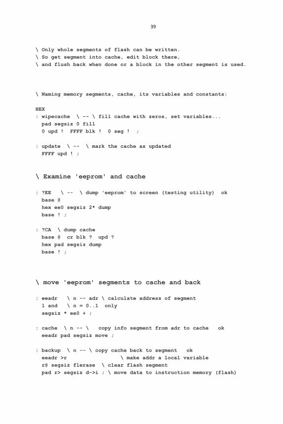
\ Only whole segments of flash can be written.
\ So get segment into cache, edit block there,
\ and flush back when done or a block in the other segment is used.
\ Naming memory segments, cache, its variables and constants:
HEX
: wipecache \ -- \ fill cache with zeros, set variables...
pad segsiz 0 fill
0 upd ! FFFF blk ! 0 seg ! ;
: update \ -- \ mark the cache as updated
FFFF upd ! ;
\ Examine 'eeprom' and cache
: ?EE \ -- \ dump 'eeprom' to screen (testing utility) ok
base @
hex ee0 segsiz 2* dump
base ! ;
: ?CA \ dump cache
base @ cr blk ? upd ?
hex pad segsiz dump
base ! ;
\ move 'eeprom' segments to cache and back
: eeadr \ n -- adr \ calculate address of segment
1 and \ n = 0..1 only
segsiz * ee0 + ;
: cache \ n -- \ copy info segment from adr to cache ok
eeadr pad segsiz move ;
: backup \ n -- \ copy cache back to segment ok
eeadr >r \ make addr a local variable
r@ segsiz flerase \ clear flash segment
pad r> segsiz d->i ; \ move data to instruction memory (flash)

40
: FLUSH \ -- \ if updated copy pad to segment ok
upd @ IF seg @ backup THEN ;
\ Move block to cache
: blkadr \ n -- adr \ calculate address of block in cache
3 and \ n = 0..3 only
blksiz * pad + ;
: BLOCK \ n -- adr \ cache block n
dup blk @ = IF blkadr exit THEN \ block is in cache already.
flush
7 and blk ! \ 0..7 blocks only
blk @ 3 > 1 and seg ! \ calculate segment
seg @ cache \ get segment
0 upd ! \ mark as unchanged
blk @ blkadr ; \ put block address on stack
\ Edit items in a block
HEX
: dolist \ adr -- \ print a block
dup blksiz + swap
DO i c@ 2# LOOP ;
: ruler \ -- \ print a block ruler
blksiz 0 DO i 2# LOOP ;
: LIST \ n -- \ list block n to screen
cr ruler
cr block dolist ;
: >> \ b n -- \ poke byte and show result.
blk @ blkadr + c! \ write byre b into n-th position
\ of current block in cache
blk @ list update ;

41
\ prg0 ee? \ test fill info segments C and D.
\ --> intermediate-stage-3.txt
\ -----------------------------------------------------------
\ EDIT a Page of memory using S1 and S2 on MyCo-board,
\ no serial interface used.
\ Edit in cache, and when done save to 'eeprom'.
\ select page
\ start at position zero in page
\ display address
\ edit high nibble
\ edit low nibble
\ autoincrement position in page
\ flush if done
\ select byte
HEX
\ more switch conditions
: S1?? \ -- f \ true if S1 is down
080 020 cget 0= ;
: S2?? \ -- f \ true if S2 is down
008 020 cget 0= ;
: S1DOWN? \ -- f \ true if S1 is held down
s1?? s1?? and s1?? and ; \ debouncing
: S2DOWN? \ -- f \ true if S2 is held down
s2?? s2?? and s2?? and ; \ debouncing
: SWAIT \ -- \ wait till switch is pressed
s1- s2- BEGIN s2? s1? or UNTIL
29 ; \ 1s delay - time to press the other switch too.
\ this works because pressing a switch is hardware detected
\ by it's falling edge
\ more indicator LED "GUI" (PWM driven LED)
: BRIGHT \ -- \ bright green LED indicating upper nibble
4F 59 ;

42
: DIMMED \ -- \ dimmed green LED indicating lower nibble
41 59 ;
: SHADED \ -- \ shaded green LED indicating lower nibble
44 59 ;
: setpwm \ n -- \ set pwm to n (n=0..F)
0040 + eval 59 23 ( delay ) ;
: SWELL \ --
0010 0006 DO i setpwm LOOP
0001 000F DO i setpwm -1 +LOOP
0006 0000 DO i setpwm LOOP
;
\ edit both nibbles in a byte
: INC-OUT \ increment OUT
out> 1+ out. ;
: EDOUT \ n -- n' \ edit nibble n using S1 to inc and S2 to exit
s1- s2- out.
BEGIN \ single step or hold down S1 to increment n
s1down?
IF inc-out 27 ( delay ) THEN
s2? UNTIL
s1- s2- \ clear flags
out> ; \ put n' on stack
: EDHI \ adr -- \ edit nibble-1 in variable at address
bright
>r
r@ 1@ edout r> 1! ;
: EDLO \ adr -- \ edit nibble-0 in variable at address
dimmed
>r
r@ 0@ edout r> 0! ;
: EDC \ adr -- \ edit byte at address of cache
sgpc ! \ save addr to cache pointer
sgpc @ c@ abcd c! \ get byte to abcd
noindi 28 \ delay
abcd edhi \ set new value in abcd nibble c
noindi 28
abcd edlo \ set new value in abcd nibble d
sgpc @ c@ abcd c@ <> \ if altered ...
IF abcd c@ sgpc @ c! update THEN ; \ store and set update flag
: EDBYTE \ -- \ edit byte at current position in current page
blk @ blkadr rtrn 0@ + edc ;

43
: SELPAGE \ -- \ select page using
\ S1 to inc and S2 to exit
swell swell swell
zero edout block drop \ make SELPAGE = BLOCK in forth
noindi ;
: SELPOS \ -- \ select position in page
rtrn 0@ edout rtrn 0! ;
\ we use variable RTRN as pointer to byte in page
: EDPAGE \ -- \ edit current page ( = block number )
zero rtrn ! \ start with byte zero
BEGIN
swell swell rtrn 0@ out.
swait s1? s2? and 0= WHILE
s2down? IF swell selpos THEN \ select position in page
\ if S2 is held down
edbyte \ edit byte at selected position
rtrn 0@ 1+ rtrn 0! \ increment position
REPEAT
flush noindi zero out.
s1- s2- ;
: SEDIT \ -- \ edit MyCo program page using S2 and S1
selpage edpage ;
\ --> intermediate-stage-4.txt
\ -----------------------------------------------------------
\ MyCo
\ User interface of MyCo:
\ Buttons S1 and S2, 4 LEDs, reset button.
HEX
: BLINK \ blink 4 LEDs to indicate wait state mk
000f out. 28 \ 500 ms delay

44
zero out. 28 ;
: MAIN
blink
s1? IF run exit THEN \ press S1 to run program
s2? IF sedit exit THEN \ press S2 to enter S1S2 edit mode
;
: Q? \ -- f \ quit - press q to leave MyCo
key? if key 0071 ( q ) = else zero then ;
: MYCO
28 \ 500 ms delay
ee0 @ IF prg0 THEN \ check, load default program
init s1- s2- noindi \ initialisation
BEGIN main Q? UNTIL ." Forth " ; \ mk0
\ --> intermediate-stage-5.txt
\ ' myco app !
\ save
\ decimal mem u.
\ todo ***
\ verify opcodes
( finis )

45
MyCo Control Instructions Michael Kalus/ Juergen Pintaske Version 0.9.1 4e4th Version 2015_04_04
Switching on Power or Reset starts MyCo program. The 4 LEDs at OUT will flash. The indicator LED (PWM LED) is switched off. Idle State - MyCo is ready and waiting for an input either via S1 / S2 or via the keyboard.
S1 - Switch pressed - MyCo program starts S2 - Switch pressed - MyCo switches ino Programming Mode – no connection to thePC required 'q' - Entered on Terminal - 4e4th Forth starts (Only works if keyboard
is connected / MyCo in dle State)
- To Run a Program already intalled- In Idle State press S1. MyCo will then enters the Program Run Mode. MyCo programs always start at page 0 address $00. To terminate a running MyCo program: press S1 or S2 key - or any key on the keyboard.
- Show the Program Flow –
A)-using the 4 LEDs --- To view the program steps from the outside, a MyCo program has to make outputs to the 4 LEDs, otherwise nothing is visible. Additional LED test output instructions can be added for debugging. Later replaced by NOPs. Extensions: Use a volt meter to check the levels at IN and OUT and to watch – or a multimeter or an oscilloscope.
B) Using Forth and the Serial Interface--- Using the additional options The MyCo Program runs using the Interactive Programming Language Forth. There are 3 additional services provided in this mode in order to test the program flow step by step. Using the space bar on the keyboard, you step through the whole program. The status of all registers and other IO are shown:

46
LOG writes the MyCo program sequence step by step. Press the space bar to step through the whole program. Register contents, state at Input Port and Output Port will be displayed. STEP displays the entire contents of the MyCo memory in one go. Here as well, step through the whole program by pressing the space bar. Registers and Ports are displayed step by step. So you see exactly at which point of the program you are and which activity has been executed (single stepping).
RUN starts the MyCo Program in Flash memory. In this way the effects on periphery can be seen. Pressing any key on the keyboard stops the MyCo program execution, and you come back to the Forth Operating System level.
- Programming – Press S2 when in Idle State. MyCo status changes into the Programming Mode. Programming of a MyCo program is done code block by block (page), then each block byte by byte, and each byte nibble by nibble. To start, first the target page must be selected that will be processed.
- Select Page - Indicator LED flashes 3 times. Using S1, one of 8 pages can be selected. Default page is page-0. Continue using S2.
- Select Bytes - By repeatedly pressing S2 one program byte after the other can be displayed. In This way all bytes of the selected page can be inspected, contents will be shown via the 4 LEDs. Here each byte is shown in three steps.

47
View Memory Contents - Press S2 repeatedly
Step Indicator LED (PWM) Description of 4 LED display 1 2x flashing in medium bright byte address within the page 2 from off -> to bright high nibble 3 from off-> to dim low nibble
The Read/Modify Modus starts at byte address zero, so the 4 LEDs are thus first all switched off. Press S2 and the Hi-nibble of the byte is displayed. S2 again, and the Lo nibble is displayed. Press again S2, and MyCo begins another 3-step display, now at byte address +1 After 16 bytes the procedure starts again at byte 0, MyCo stays on same page (wrap around). - Edit a Nibble - In Step_2 or Step_3 the contents of a nibble can increment by pressing S1. After $F the value is back to zero. You can step through the value as often as needed. End of nibble change input with S2. - Select Byte Start Address – If in step_1 button S2 is kept pressed, MyCo jumps into Start Address Select. Indicator LED flashes 1x, LEDs show the current byte address, incremented via S1. If new address set, S2 changes mode back to 3 step display from the new adddress. - End Editing and Transfer and Program into FLASH Memory - Press both buttons, S2 + S1 simultaneously; Back to IDLE Mode, 4 LEDs flash, at the same time edited page is written back to Flash memory. MyCo returns to IDLE MODE. In this case, changes to the nibbles are transferred to the 'eeprom'.

48
9.1 The Simulator and the Row of Buttons |-- EXIT the program
| |-- CREATE a NEW program ( Control+N )
| | |-- OPEN a file ( Control+O )
| | | |-- SAVE the actual program ( Control + S )
| | | | |-- ADD a new line to the program
| | | | | |-- DELETE the actual line
| | | | | | |-- SHOW the actual programming file
| | | | | | | |-- UPLOAD the program to the target ( Control+U )
| | | | | | | | |-- CREATE a HEX file
| | | | | | | | | |-- EXECUTE a single instruction ( F5 )
| | | | | | | | | | |-- Execute the next step ( F8 )
| | | | | | | | | | | |-- STOP the debug program execution ( F6 )
| | | | | | | | | | | | | -- START / STOP program execution ( F9)
| | | | | | | | | | | | | |-SELECT target Holtek-Mega8-TINY84-Arduino
Memory: Showing the memory locations where the instructions are stored
Instruction: Instruction to be executed at the memory execution
Data: Data related to the instruction
Description: Automatically added description
Comment: Own comment to be added
Instruction: Instruction to be inserted into the current memory location
Data: Then open Data and select related number or function

49
9.2 - The Function Window - on the right hand side
PRG / Program SEL / Select INPUTS:
Input 1 – 4 The four inputs to be set by mouse click
ADC 1, 2 Two simulated analog inputs – input a number between 0 … 255
RC1, 2 Two simulated RC servo outputs – input a number between 0 … 255
OUTPUTS:
Output 1 – 4 The four output bits sent by the PLC – Programmable Logic Controller
PWM 1, 2 Pulse Width Modulated outputs, an ON / OFF rectangular output signal
Servo 1, 2 RC servo outputs, simulating the angle by showing a number plus icon Tone: A sound to be output – to be added later
INTERNAL DATA of this PLC: The inputs are fed via the instructions into registers
RA, RB, RC, RD, ( RE, RF ) and processed
Addr The current memory location addressed
Page Each memory block page consists of 16 locations, the page display changes accordingly
And JUMPs will setting up a PAGE number if different
Radr RETURN ADDRESS – if subroutine is called, return address is shown here
DELAY Showing time is a delay instruction is executed ( SKIP If a skip decision is executed, 1 indicates jump over next instruction ) tbd

50
9.3 - Instruction Table Instruction Set shaded in yellow aextensions of ArduinoSPS/ATTiny84 version.
0 1 2 3 4 5 6 7
n.n. Port Delay Jump back rel
A= „=A“ A= A= Options
0 NOP off 1ms 0 0 A<->B
1 1 2ms 1 1 B=A A=B A=A + 1
2 2 5ms 2 2 C=A A=C A=A - 1
3 3 10ms 3 3 D=A A=D A=A + B
4 4 20ms 4 4 Dout=A Din A=A - B
5 5 50ms 5 5 Dout.0=A.0 Din.0 A=A * B
6 6 100ms 6 6 Dout.1=A.0 Din.1 A=A / B
7 7 200ms 7 7 Dout.2=A.0 Din.2 A=A and B
8 8 500ms 8 8 Dout.3=A.0 Din.3 A=A or B
9 9 1s 9 9 PWM.0=A ADC.0 A=A xor B
a 10 2s 10 10 PWM.1=A ADC.1 A= not A
b 11 5s 11 11 Servo.0=A RCin.0 A= A % B (Rem.)
c 12 10s 12 12 Servo.1=A RCin.1 A= A + 16 * B
d 13 20s 13 13 E=A A=E A= B - A
e 14 30s 14 14 F=A A=F
f 15 60s 15 15 Push A Pop A
8 9 a b c d e f
Page Jump
absolute
C* D* Skip if Call # +
(16* Page)
Callsub
/Ret
Byte Instr.
0 0 0 0 A=0 0 ret A=ADC.0
1 1 1 1 A>B 1 Call 1 A=ADC.1
2 2 2 2 A<B 2 2 A=RCin.0
3 3 3 3 A=B 3 3 A=RCin.1
4 4 4 4 Din.0=1 4 4 PWM.0=A
5 5 5 5 Din.1=1 5 5 PWM.1=A
6 6 6 6 Din.2=1 6 6 Servo.0=A
7 7 7 7 Din.3=1 7 Servo.1=A
8 8 8 8 Din.0=0 8 Def 1
9 9 9 9 Din.1=0 9 2
10 10 10 10 Din.2=0 10 3
11 11 11 11 Din.3=0 11 4
12 12 12 12 S_PRG=0 12 5
13 13 13 13 S_SEL=0 13 6
14 14 14 14 S_PRG=1 14
15 15 15 15 S_SEL=1 15 restart PrgEnd

51
9.4 - TPS / SPS Emulator http://wkla.no-ip.biz/ArduinoWiki/doku.php?id=arduino:arduinosps:spsemu
Switch top left to English if needed. Copied from Willie’s website
For the TPS PLC (and my extensions) I once wrote an emulator as a fun project.
Here the result.
The complete project is programmed in Lazarus (Freepascal).
The emulator can work with the different instruction sets of different TPS versions.
On the left you can see the programming window.
This can either be typed in directly or generated via the two combo boxes below.
There you can select the possible commands – dependent on the target selected of
the included versions.
The commands can then be executed via the 4 buttons in the top center block.
The first button tests the currently selected command (jumps are not carried out)
The second button executes the program in single-step mode.
The third button stops single-step mode
The fourth button is Start-Stop, to run at maximum speed.
In the left window you make the entries and view the results as you step through the
program.