Embed Size (px)
Citation preview

Lab #1: Schematic Entry and Simulation
Revised 4/2/2015
INTRODUCTION
In this lab you will learn how to use Mentor Graphics Design Architect IC (DAIC) to construct and simulate a schematic for an inverter. You will create theschematic which specifies transistor sizes and their interconnection. You will verify the schematic functions correctly and determine the switchingcharacteristics of your inverter. Finally, you will prepare your schematic for layout and examine a spice listing of your design.
DESIGN FLOW
In order to efficiently manage design complexity, you will employ hierarchical design methods. It is typical when doing full-custom integrated circuits to do atop-down design followed by a bottom-up implementation. You will use the bolded portions of the design flow shown below:
Initial designCapture the design as a schematicSimulate your design to verify operationCreate a symbol of your designCreate viewpoints for downstream applicationsCreate a netlistLayout a cell for this design (IC station)Verify layoutCheck for layout rule violations (DRC)Check layout against schematic (LVS)Verify circuit operation including layout parasiticsExtract parasitics and back annotate the designRe-simulate
ENTERING INFORMATION
Information can be entered in DAIC via the keyboard or mouse, or a combination of the two.
Important Shortcut Keys for DAIC:
F2: Unselect everything. Use frequently to avoid accidentally moving or deleting selected items.Esc: Terminate the current operation. Use to quit adding wires or gates.Shift-F7: Change text covered by the cursor. Use to change net names, port names, widths.Shift-F8: Zoom to fit window.Numeric Pad +: Zoom in.Numeric Pad -: Zoom out.Page Up: Move window up (object down).Page Down: Move window down (object up).Ctl-Page Up: Move window left (object right).Ctl-Page Down: Move window right (object left).
Using Strokes in DAIC:
A stroke is created by holding down the middle mouse button and moving the mouse. A list of strokes used in the schematic entry portion of DAICis shown below and can be displayed by drawing a question mark while pressing the middle mouse button.

1. PREPARE YOUR WORKSPACE
1.1 Login to one of the Linux stations, either directly, or ssh in from another source.
1.2 In your home directory, navigate to where you want to place your files for this class. Create a class directory for your work this quarter:
>> mkdir engr434 >> cd engr434
Make sure and change into the engr434 class directory anytime that you login and plan to create new designs for this class.
2. CREATE A SCHEMATIC OF A CMOS INVERTER
2.1 Create a directory for this lab and move into it. Then start the script that sets up the environment for DAIC:
>> mkdir lab1 >> cd lab1 >> daic &
2.2 Left-click on the Schematic button in the Open portion of the session palette on the right of the screen to create a new schematic. You will seea dialog box as shown.
2.3 Carefully place the cursor at the end of the Component: name (immediately following $MGC_WD), then left click once. Now type a slash "/"followed by your component name "inv1". The dialog box should look as shown below. Click OK to create your inverter schematic.
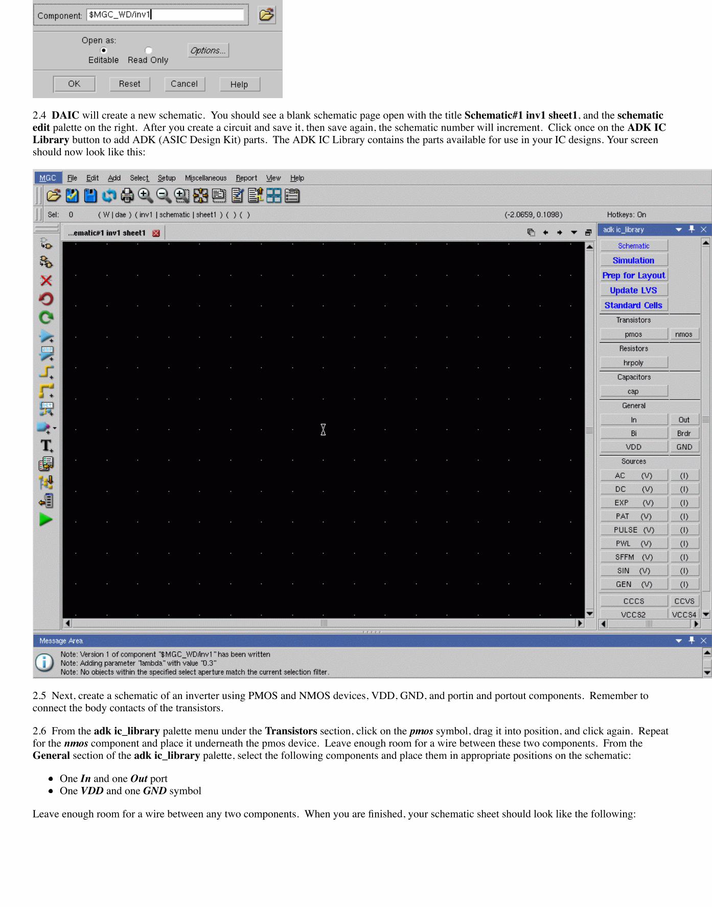
2.4 DAIC will create a new schematic. You should see a blank schematic page open with the title Schematic#1 inv1 sheet1, and the schematicedit palette on the right. After you create a circuit and save it, then save again, the schematic number will increment. Click once on the ADK ICLibrary button to add ADK (ASIC Design Kit) parts. The ADK IC Library contains the parts available for use in your IC designs. Your screenshould now look like this:
2.5 Next, create a schematic of an inverter using PMOS and NMOS devices, VDD, GND, and portin and portout components. Remember toconnect the body contacts of the transistors.
2.6 From the adk ic_library palette menu under the Transistors section, click on the pmos symbol, drag it into position, and click again. Repeatfor the nmos component and place it underneath the pmos device. Leave enough room for a wire between these two components. From theGeneral section of the adk ic_library palette, select the following components and place them in appropriate positions on the schematic:
One In and one Out portOne VDD and one GND symbol
Leave enough room for a wire between any two components. When you are finished, your schematic sheet should look like the following:
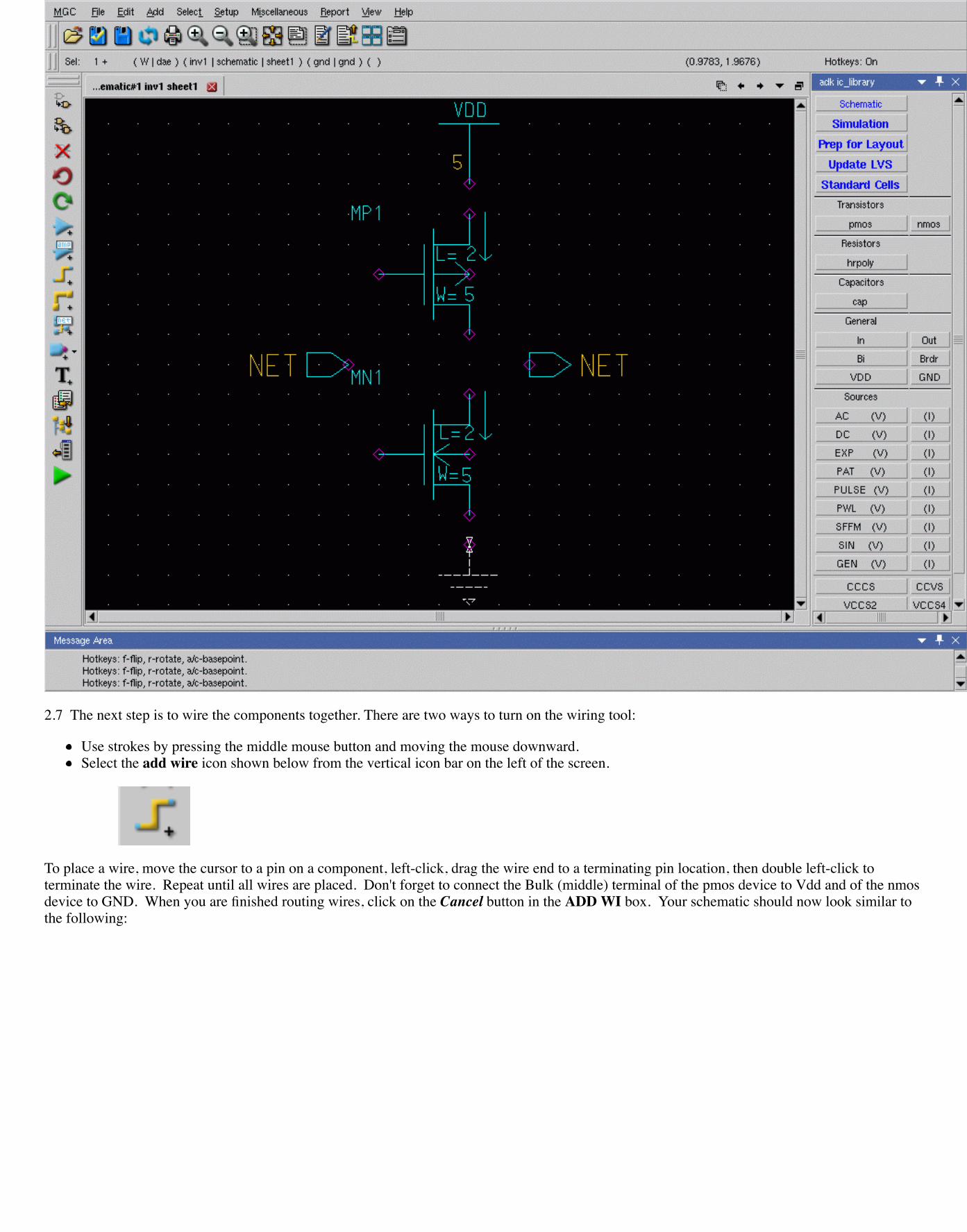
2.7 The next step is to wire the components together. There are two ways to turn on the wiring tool:
Use strokes by pressing the middle mouse button and moving the mouse downward.Select the add wire icon shown below from the vertical icon bar on the left of the screen.
To place a wire, move the cursor to a pin on a component, left-click, drag the wire end to a terminating pin location, then double left-click toterminate the wire. Repeat until all wires are placed. Don't forget to connect the Bulk (middle) terminal of the pmos device to Vdd and of the nmosdevice to GND. When you are finished routing wires, click on the Cancel button in the ADD WI box. Your schematic should now look similar tothe following:
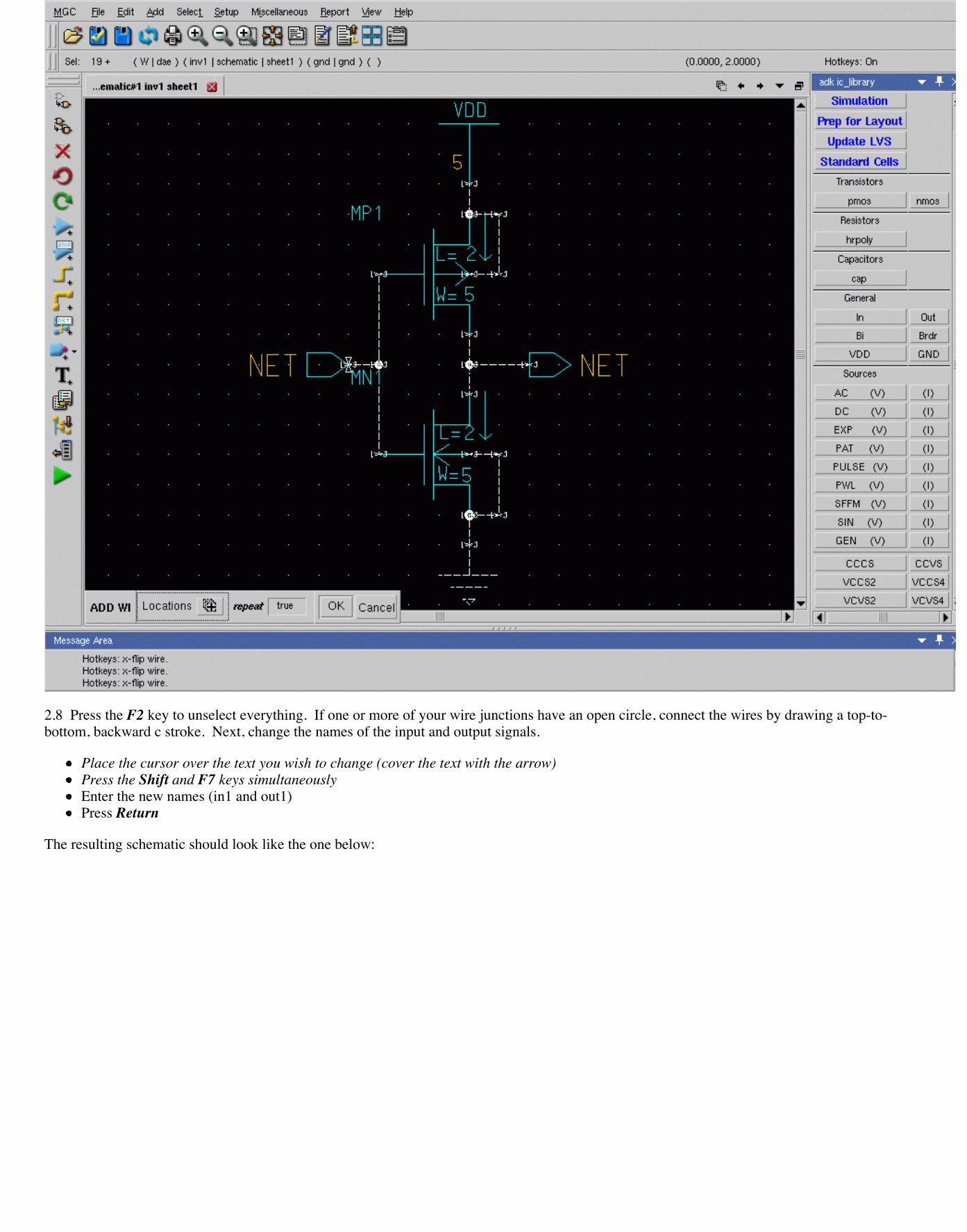
2.8 Press the F2 key to unselect everything. If one or more of your wire junctions have an open circle, connect the wires by drawing a top-to-bottom, backward c stroke. Next, change the names of the input and output signals.
Place the cursor over the text you wish to change (cover the text with the arrow)Press the Shift and F7 keys simultaneouslyEnter the new names (in1 and out1)Press Return
The resulting schematic should look like the one below:
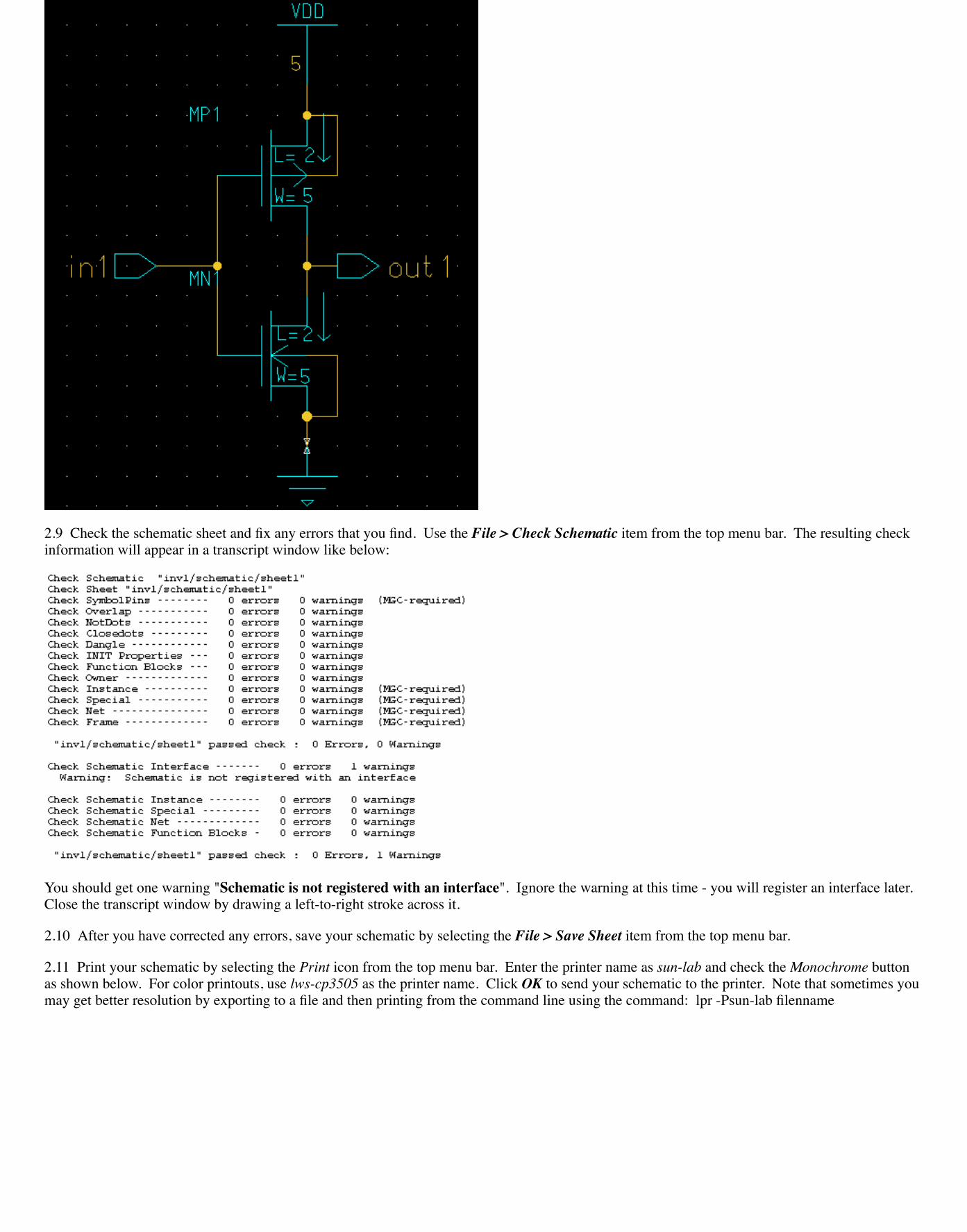
2.9 Check the schematic sheet and fix any errors that you find. Use the File > Check Schematic item from the top menu bar. The resulting checkinformation will appear in a transcript window like below:
You should get one warning "Schematic is not registered with an interface". Ignore the warning at this time - you will register an interface later. Close the transcript window by drawing a left-to-right stroke across it.
2.10 After you have corrected any errors, save your schematic by selecting the File > Save Sheet item from the top menu bar.
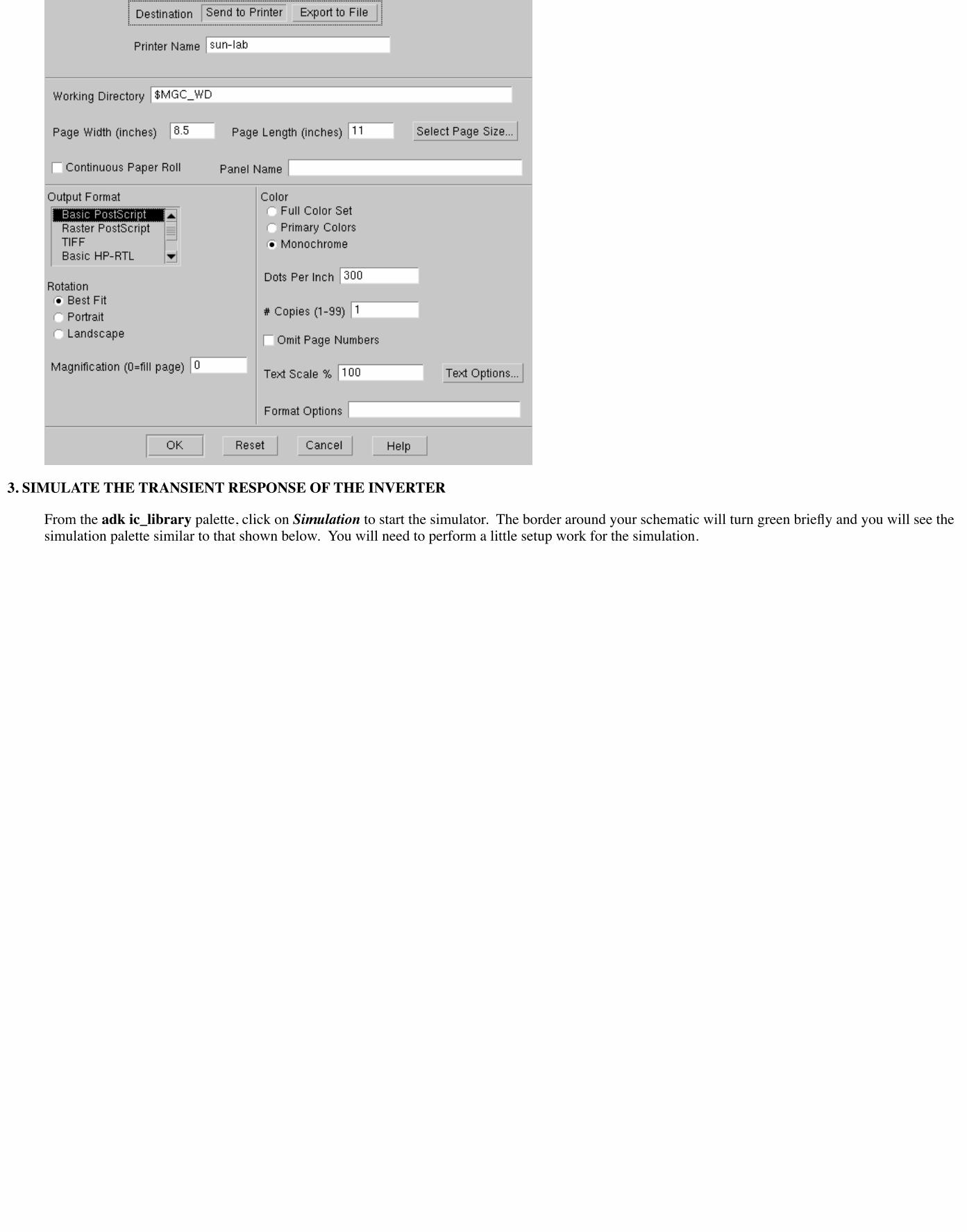
2.11 Print your schematic by selecting the Print icon from the top menu bar. Enter the printer name as sun-lab and check the Monochrome buttonas shown below. For color printouts, use lws-cp3505 as the printer name. Click OK to send your schematic to the printer. Note that sometimes youmay get better resolution by exporting to a file and then printing from the command line using the command: lpr -Psun-lab filenname
3. SIMULATE THE TRANSIENT RESPONSE OF THE INVERTER
From the adk ic_library palette, click on Simulation to start the simulator. The border around your schematic will turn green briefly and you will see thesimulation palette similar to that shown below. You will need to perform a little setup work for the simulation.
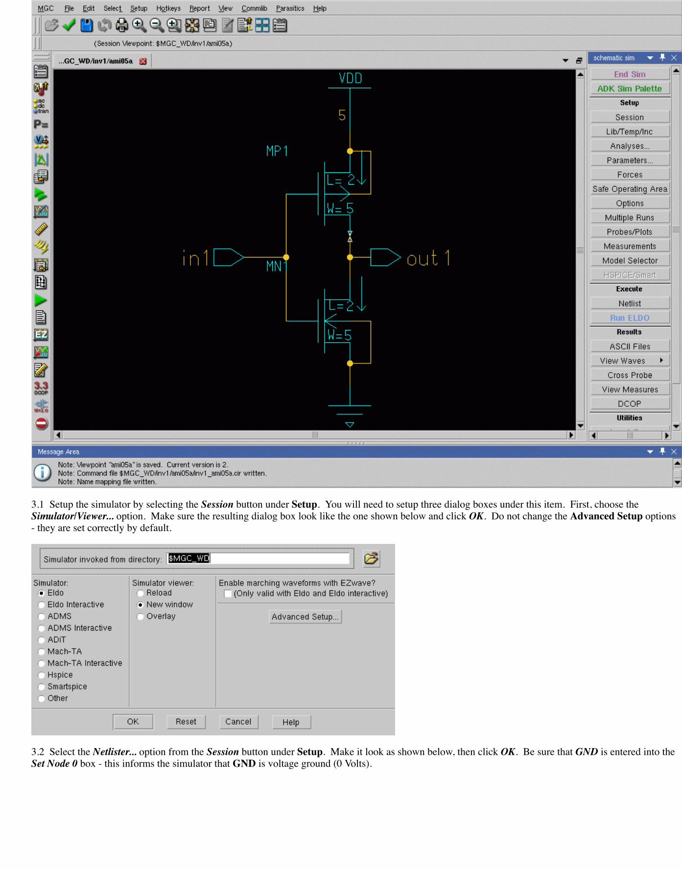
3.1 Setup the simulator by selecting the Session button under Setup. You will need to setup three dialog boxes under this item. First, choose theSimulator/Viewer... option. Make sure the resulting dialog box look like the one shown below and click OK. Do not change the Advanced Setup options- they are set correctly by default.
3.2 Select the Netlister... option from the Session button under Setup. Make it look as shown below, then click OK. Be sure that GND is entered into theSet Node 0 box - this informs the simulator that GND is voltage ground (0 Volts).
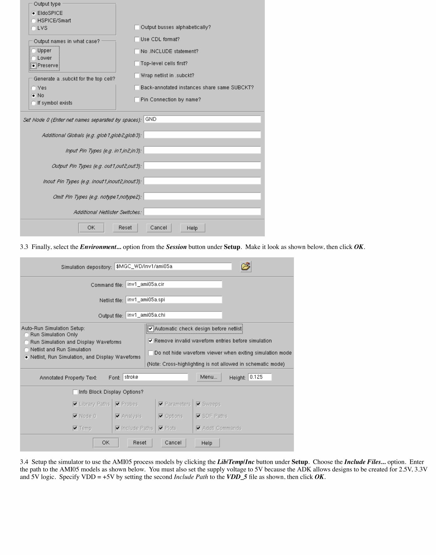
3.3 Finally, select the Environment... option from the Session button under Setup. Make it look as shown below, then click OK.
3.4 Setup the simulator to use the AMI05 process models by clicking the Lib/Temp/Inc button under Setup. Choose the Include Files... option. Enterthe path to the AMI05 models as shown below. You must also set the supply voltage to 5V because the ADK allows designs to be created for 2.5V, 3.3Vand 5V logic. Specify VDD = +5V by setting the second Include Path to the VDD_5 file as shown, then click OK.
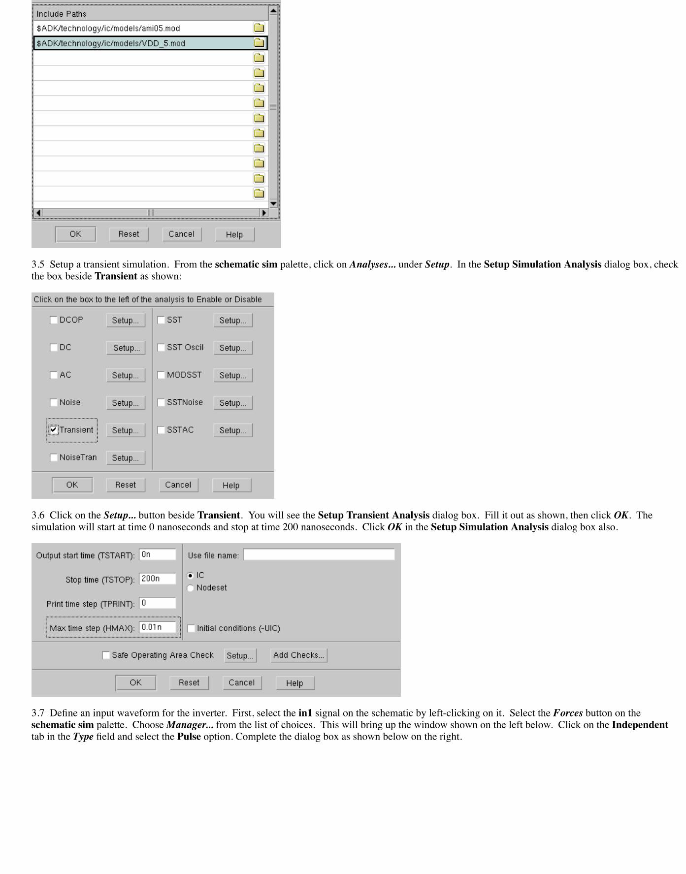
3.5 Setup a transient simulation. From the schematic sim palette, click on Analyses... under Setup. In the Setup Simulation Analysis dialog box, checkthe box beside Transient as shown:
3.6 Click on the Setup... button beside Transient. You will see the Setup Transient Analysis dialog box. Fill it out as shown, then click OK. Thesimulation will start at time 0 nanoseconds and stop at time 200 nanoseconds. Click OK in the Setup Simulation Analysis dialog box also.
3.7 Define an input waveform for the inverter. First, select the in1 signal on the schematic by left-clicking on it. Select the Forces button on theschematic sim palette. Choose Manager... from the list of choices. This will bring up the window shown on the left below. Click on the Independenttab in the Type field and select the Pulse option. Complete the dialog box as shown below on the right.
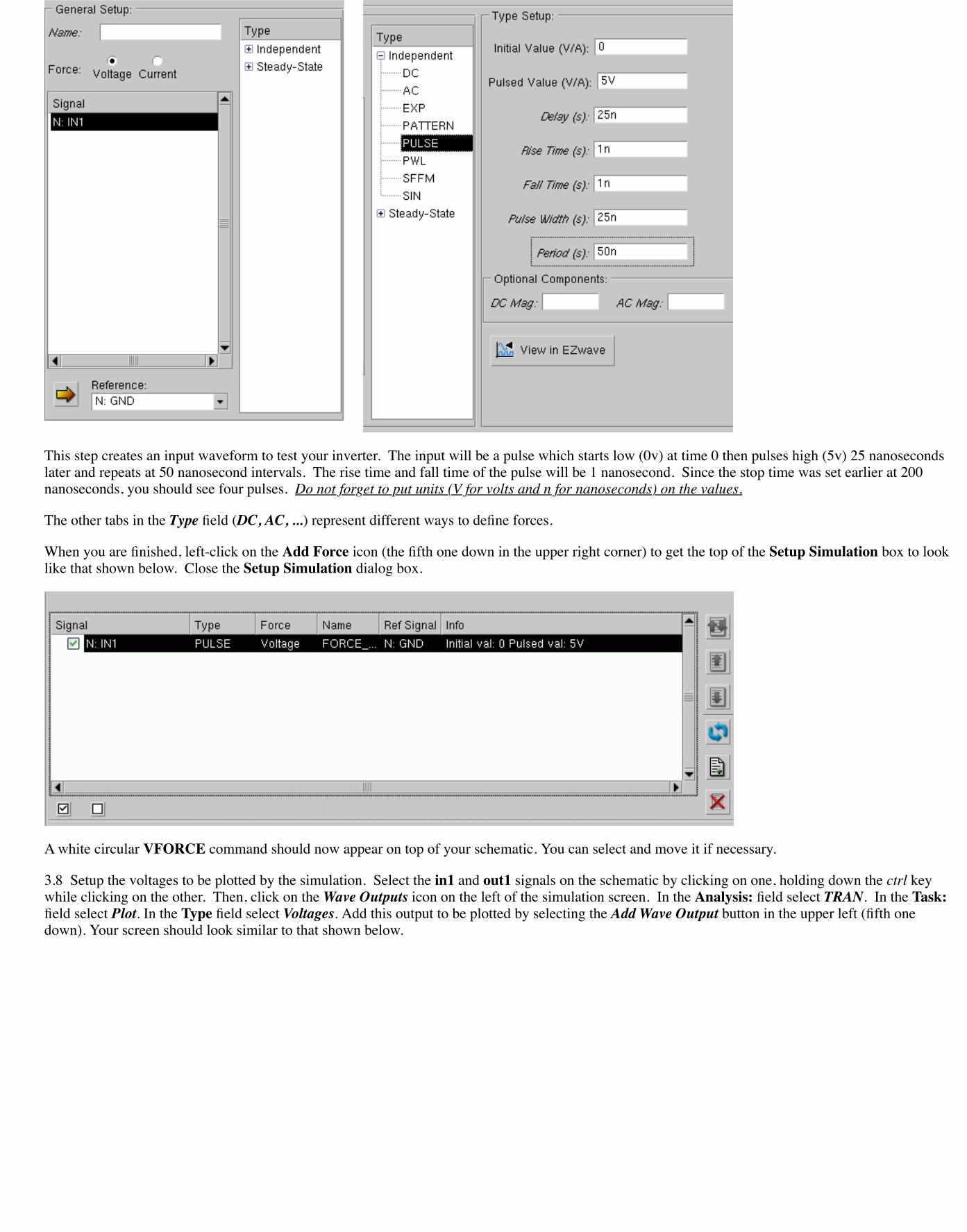
This step creates an input waveform to test your inverter. The input will be a pulse which starts low (0v) at time 0 then pulses high (5v) 25 nanosecondslater and repeats at 50 nanosecond intervals. The rise time and fall time of the pulse will be 1 nanosecond. Since the stop time was set earlier at 200nanoseconds, you should see four pulses. Do not forget to put units (V for volts and n for nanoseconds) on the values.
The other tabs in the Type field (DC, AC, ...) represent different ways to define forces.
When you are finished, left-click on the Add Force icon (the fifth one down in the upper right corner) to get the top of the Setup Simulation box to looklike that shown below. Close the Setup Simulation dialog box.
A white circular VFORCE command should now appear on top of your schematic. You can select and move it if necessary.
3.8 Setup the voltages to be plotted by the simulation. Select the in1 and out1 signals on the schematic by clicking on one, holding down the ctrl keywhile clicking on the other. Then, click on the Wave Outputs icon on the left of the simulation screen. In the Analysis: field select TRAN. In the Task:field select Plot. In the Type field select Voltages. Add this output to be plotted by selecting the Add Wave Output button in the upper left (fifth onedown). Your screen should look similar to that shown below.
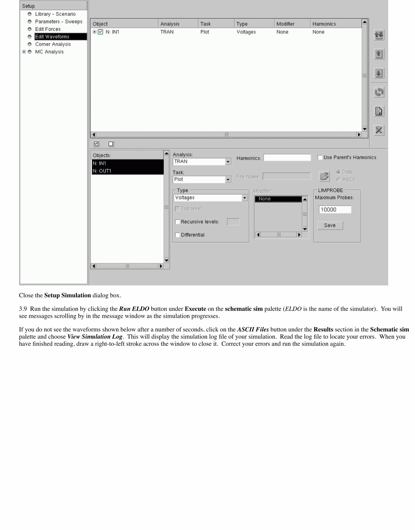
Close the Setup Simulation dialog box.
3.9 Run the simulation by clicking the Run ELDO button under Execute on the schematic sim palette (ELDO is the name of the simulator). You willsee messages scrolling by in the message window as the simulation progresses.
If you do not see the waveforms shown below after a number of seconds, click on the ASCII Files button under the Results section in the Schematic simpalette and choose View Simulation Log. This will display the simulation log file of your simulation. Read the log file to locate your errors. When youhave finished reading, draw a right-to-left stroke across the window to close it. Correct your errors and run the simulation again.
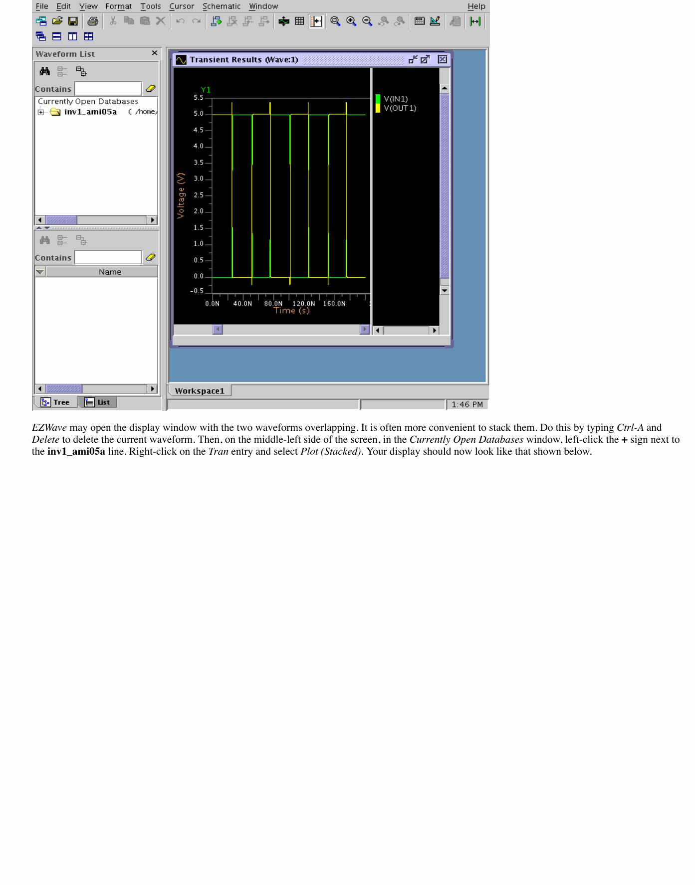
EZWave may open the display window with the two waveforms overlapping. It is often more convenient to stack them. Do this by typing Ctrl-A andDelete to delete the current waveform. Then, on the middle-left side of the screen, in the Currently Open Databases window, left-click the + sign next tothe inv1_ami05a line. Right-click on the Tran entry and select Plot (Stacked). Your display should now look like that shown below.
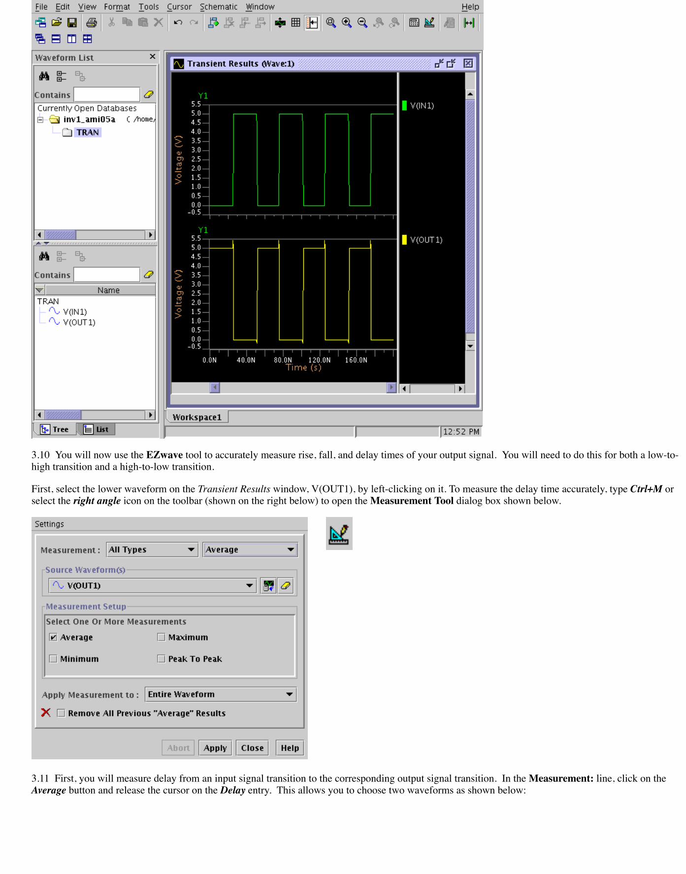
3.10 You will now use the EZwave tool to accurately measure rise, fall, and delay times of your output signal. You will need to do this for both a low-to-high transition and a high-to-low transition.
First, select the lower waveform on the Transient Results window, V(OUT1), by left-clicking on it. To measure the delay time accurately, type Ctrl+M orselect the right angle icon on the toolbar (shown on the right below) to open the Measurement Tool dialog box shown below.
3.11 First, you will measure delay from an input signal transition to the corresponding output signal transition. In the Measurement: line, click on theAverage button and release the cursor on the Delay entry. This allows you to choose two waveforms as shown below:
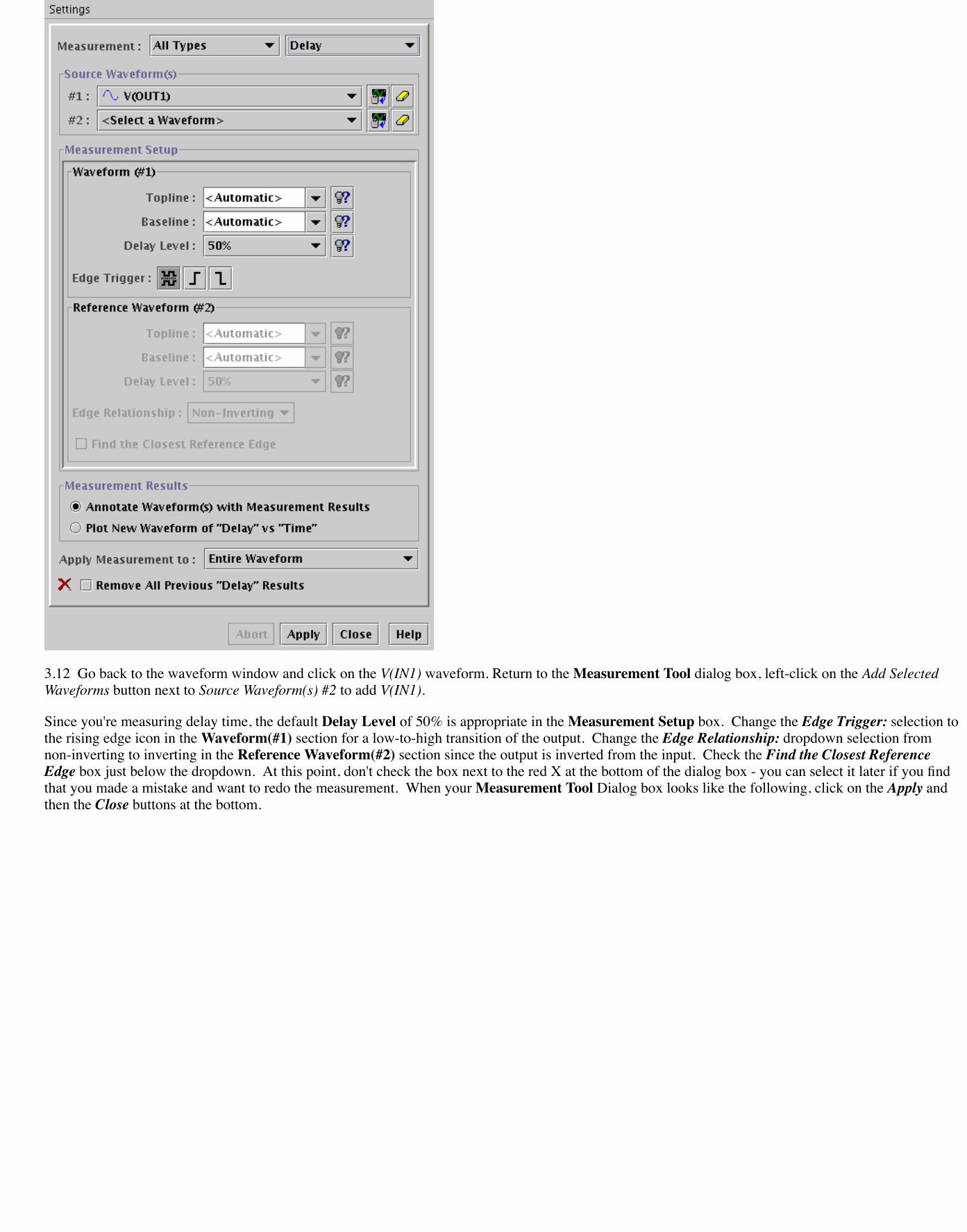
3.12 Go back to the waveform window and click on the V(IN1) waveform. Return to the Measurement Tool dialog box, left-click on the Add SelectedWaveforms button next to Source Waveform(s) #2 to add V(IN1).
Since you're measuring delay time, the default Delay Level of 50% is appropriate in the Measurement Setup box. Change the Edge Trigger: selection tothe rising edge icon in the Waveform(#1) section for a low-to-high transition of the output. Change the Edge Relationship: dropdown selection fromnon-inverting to inverting in the Reference Waveform(#2) section since the output is inverted from the input. Check the Find the Closest ReferenceEdge box just below the dropdown. At this point, don't check the box next to the red X at the bottom of the dialog box - you can select it later if you findthat you made a mistake and want to redo the measurement. When your Measurement Tool Dialog box looks like the following, click on the Apply andthen the Close buttons at the bottom.
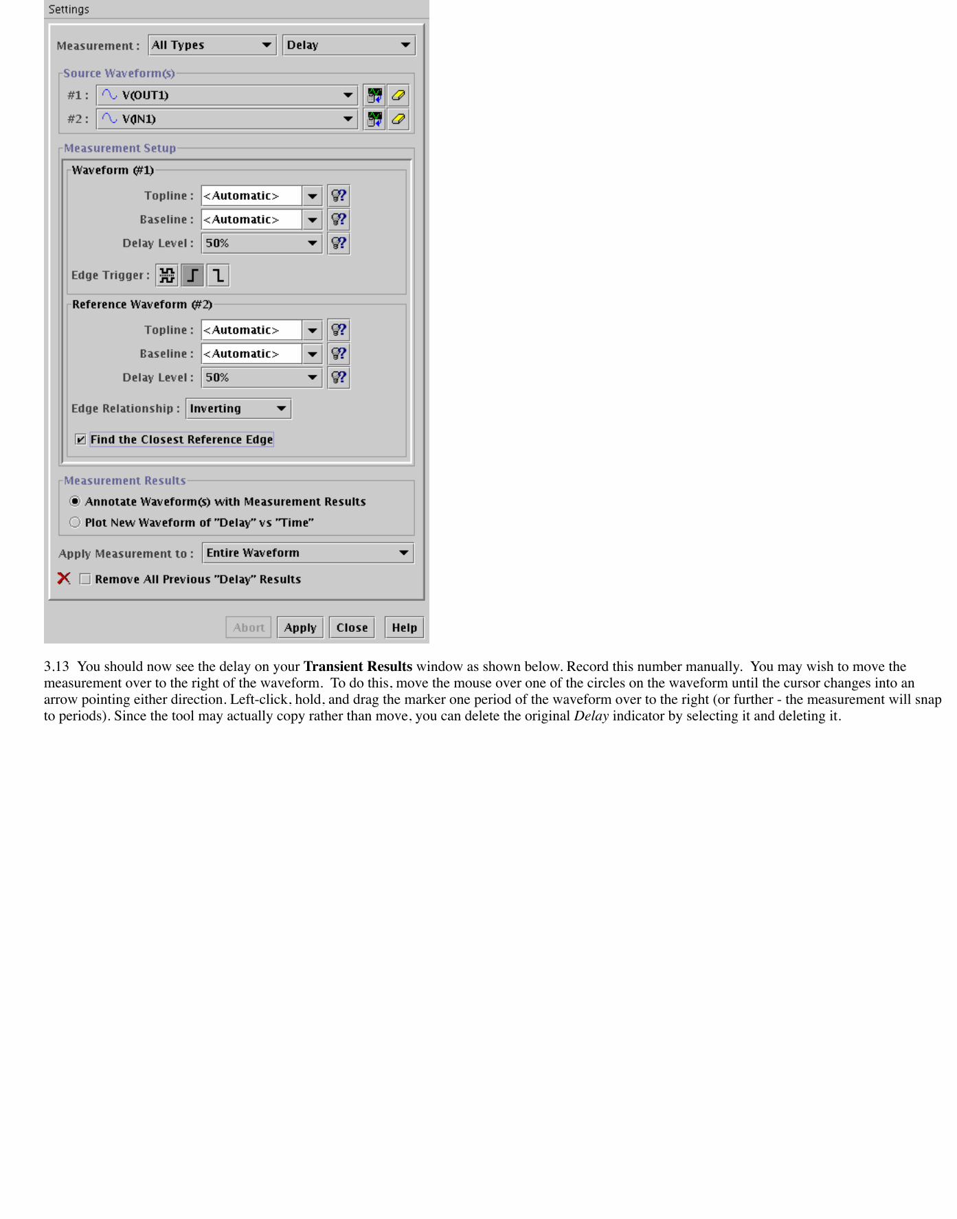
3.13 You should now see the delay on your Transient Results window as shown below. Record this number manually. You may wish to move themeasurement over to the right of the waveform. To do this, move the mouse over one of the circles on the waveform until the cursor changes into anarrow pointing either direction. Left-click, hold, and drag the marker one period of the waveform over to the right (or further - the measurement will snapto periods). Since the tool may actually copy rather than move, you can delete the original Delay indicator by selecting it and deleting it.
3.14 To measure the high-to-low output transition, select the falling edge icon in the Measurement Tool box (under Waveform(#1), Edge Trigger:). Make sure you are still inverting and finding the closest reference edge and make sure that the Remove All Previous "Delay" Results tab is not selected -this way, you'll keep your low-to-high measurement and add the high-to-low measurement. Left-click Apply. Move the measurement further into yourwaveform if desired. Your results should be similar to those shown below. Note that the delay times are not equal. Record this new number.
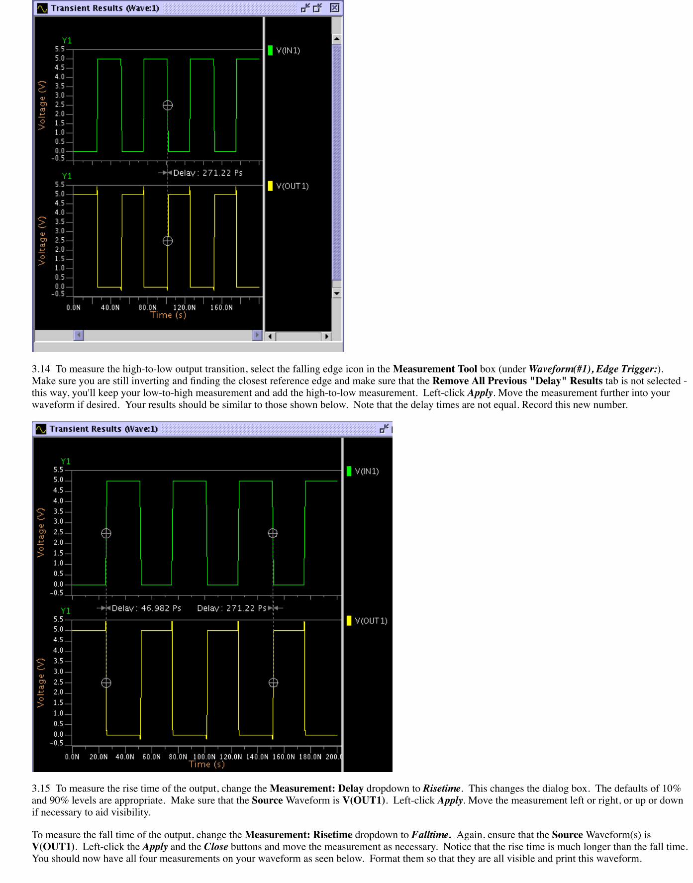
3.15 To measure the rise time of the output, change the Measurement: Delay dropdown to Risetime. This changes the dialog box. The defaults of 10%and 90% levels are appropriate. Make sure that the Source Waveform is V(OUT1). Left-click Apply. Move the measurement left or right, or up or downif necessary to aid visibility.
To measure the fall time of the output, change the Measurement: Risetime dropdown to Falltime. Again, ensure that the Source Waveform(s) isV(OUT1). Left-click the Apply and the Close buttons and move the measurement as necessary. Notice that the rise time is much longer than the fall time.You should now have all four measurements on your waveform as seen below. Format them so that they are all visible and print this waveform.
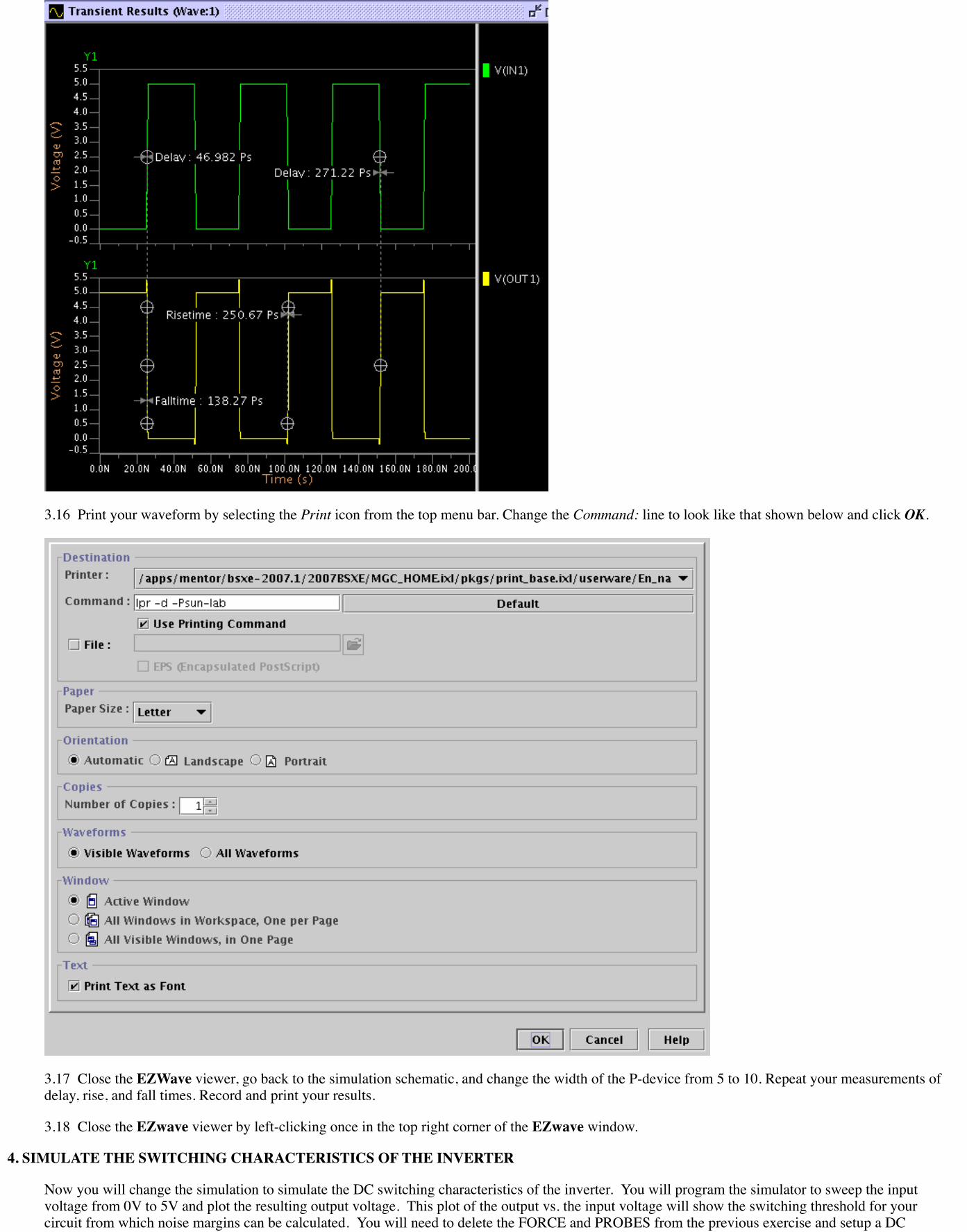
3.16 Print your waveform by selecting the Print icon from the top menu bar. Change the Command: line to look like that shown below and click OK.
3.17 Close the EZWave viewer, go back to the simulation schematic, and change the width of the P-device from 5 to 10. Repeat your measurements ofdelay, rise, and fall times. Record and print your results.
3.18 Close the EZwave viewer by left-clicking once in the top right corner of the EZwave window.
4. SIMULATE THE SWITCHING CHARACTERISTICS OF THE INVERTER
Now you will change the simulation to simulate the DC switching characteristics of the inverter. You will program the simulator to sweep the inputvoltage from 0V to 5V and plot the resulting output voltage. This plot of the output vs. the input voltage will show the switching threshold for yourcircuit from which noise margins can be calculated. You will need to delete the FORCE and PROBES from the previous exercise and setup a DC
analysis instead of a transient analysis.
4.1 From the schematic sim palette, delete the previous FORCE by left clicking on the white circle and pressing Delete.
4.2 Delete the previous PROBES by left-clicking on the Wave Outputs button, selecting the lone entry, and left-clicking the Remove Selectedbutton (the one with the red X through it). Close the Setup Simulation dialog box.
4.3 Add a DC force to the input signal (you will need a DC force to sweep for voltage characteristics) by first selecting the in1 signal in theschematic window. Click on the Forces > Manager... button. Select the DC Type of force and enter 5V as the magnitude. Click the Add Forcebutton and exit this screen. You have now defined a DC force necessary for the sweep.
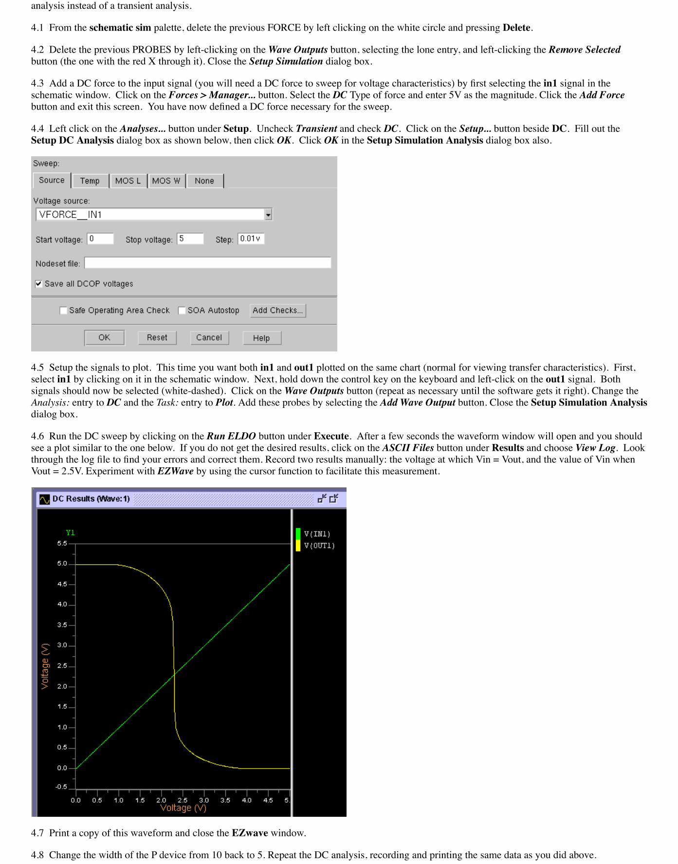
4.4 Left click on the Analyses... button under Setup. Uncheck Transient and check DC. Click on the Setup... button beside DC. Fill out theSetup DC Analysis dialog box as shown below, then click OK. Click OK in the Setup Simulation Analysis dialog box also.
4.5 Setup the signals to plot. This time you want both in1 and out1 plotted on the same chart (normal for viewing transfer characteristics). First,select in1 by clicking on it in the schematic window. Next, hold down the control key on the keyboard and left-click on the out1 signal. Bothsignals should now be selected (white-dashed). Click on the Wave Outputs button (repeat as necessary until the software gets it right). Change theAnalysis: entry to DC and the Task: entry to Plot. Add these probes by selecting the Add Wave Output button. Close the Setup Simulation Analysisdialog box.
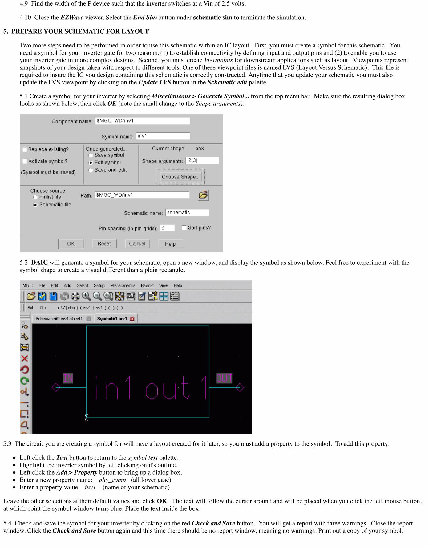
4.6 Run the DC sweep by clicking on the Run ELDO button under Execute. After a few seconds the waveform window will open and you shouldsee a plot similar to the one below. If you do not get the desired results, click on the ASCII Files button under Results and choose View Log. Lookthrough the log file to find your errors and correct them. Record two results manually: the voltage at which Vin = Vout, and the value of Vin whenVout = 2.5V. Experiment with EZWave by using the cursor function to facilitate this measurement.
4.7 Print a copy of this waveform and close the EZwave window.
4.8 Change the width of the P device from 10 back to 5. Repeat the DC analysis, recording and printing the same data as you did above.
4.9 Find the width of the P device such that the inverter switches at a Vin of 2.5 volts.
4.10 Close the EZWave viewer. Select the End Sim button under schematic sim to terminate the simulation.
5. PREPARE YOUR SCHEMATIC FOR LAYOUT
Two more steps need to be performed in order to use this schematic within an IC layout. First, you must create a symbol for this schematic. Youneed a symbol for your inverter gate for two reasons, (1) to establish connectivity by defining input and output pins and (2) to enable you to useyour inverter gate in more complex designs. Second, you must create Viewpoints for downstream applications such as layout. Viewpoints representsnapshots of your design taken with respect to different tools. One of these viewpoint files is named LVS (Layout Versus Schematic). This file isrequired to insure the IC you design containing this schematic is correctly constructed. Anytime that you update your schematic you must alsoupdate the LVS viewpoint by clicking on the Update LVS button in the Schematic edit palette.
5.1 Create a symbol for your inverter by selecting Miscellaneous > Generate Symbol... from the top menu bar. Make sure the resulting dialog boxlooks as shown below, then click OK (note the small change to the Shape arguments).
5.2 DAIC will generate a symbol for your schematic, open a new window, and display the symbol as shown below. Feel free to experiment with thesymbol shape to create a visual different than a plain rectangle.
5.3 The circuit you are creating a symbol for will have a layout created for it later, so you must add a property to the symbol. To add this property:
Left click the Text button to return to the symbol text palette.Highlight the inverter symbol by left clicking on it's outline.Left click the Add > Property button to bring up a dialog box.Enter a new property name: phy_comp (all lower case)Enter a property value: inv1 (name of your schematic)
Leave the other selections at their default values and click OK. The text will follow the cursor around and will be placed when you click the left mouse button,at which point the symbol window turns blue. Place the text inside the box.
5.4 Check and save the symbol for your inverter by clicking on the red Check and Save button. You will get a report with three warnings. Close the reportwindow. Click the Check and Save button again and this time there should be no report window, meaning no warnings. Print out a copy of your symbol.

5.5 Return to your inverter schematic by selecting the schematic tab near the top of the symbol window. This will change the palette on the right to theschematic edit palette. Create downstream viewpoints describing your schematic by clicking on the Prep for Layout button. This will take a few seconds asDAIC prepares various viewpoints of your schematic. When it completes, you will see a transcript in the Message Area similar to the one below. DAIC alwayswrites a netlist (spice file) to [component_name]/[component name].src.net, in this case inv1/inv1.src.net, in your current working directory. You now have asymbol and a spice file for use with downstream applications.
5.6 Close DAIC. Go to a Unix command window and type in the following command to display your spice file. Your command window shouldappear similar to the one shown below. Note the global power connections, the two signals (in1 and out1), the two transistors (MN1 and MP1) andtheir widths and lengths.
>> more inv1/inv1.src.net
6. TO TURN IN
The following information is due at the beginning of the first class period following this lab. Staple the following items together in the order shownbelow. Each person must turn in a complete set of documentation.
A one page or less description stating your overall simulation results. Include a table showing your measurements of delays, rise times, andfall times. State your general observations, but since you probably don't yet know why you got the results you did, leave the analysis until alater lab writeup.Results from section 4.9 of this handout.Schematic diagram of your circuit. Include one schematic page for your inverter and one page for your symbol.Simulation waveforms from EZwave. Make sure you have proper resolution.A command file from simulation printed from the Unix prompt (lpr –Psun-lab inv1/ami05a/inv1_ami05a.cir)A netlist file from simulation, also printed from the Unix prompt (lpr –Psun-lab inv1/ami05a/inv1_ami05a.spi)
Based on tutorials prepared by David Zar and Robert Klencke.Send comments to [email protected]


![[ASM] Lab1](https://img.dokumen.tips/doc/110x75/588121881a28abb9388b706b/asm-lab1.jpg)