Embed Size (px)
Citation preview
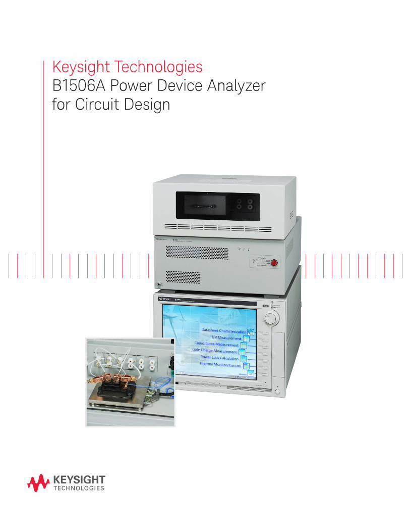
Keysight Technologies B1506A Power Device Analyzer for Circuit Design
2
The B1506A eliminates power device performance uncertainties for circuit designers
Do you have conidence that your circuit will function correctly in mission critical applications?
Do you worry about having to recall thousands of products because you used faulty devices in your circuits?
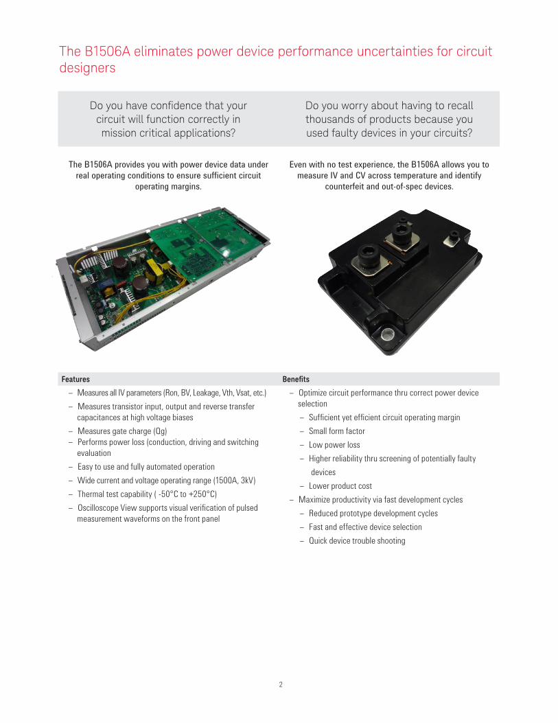
The B1506A provides you with power device data under
real operating conditions to ensure sufficient circuit
operating margins.
Even with no test experience, the B1506A allows you to
measure IV and CV across temperature and identify
counterfeit and out-of-spec devices.
Features Beneits
– Measures all IV parameters (Ron, BV, Leakage, Vth, Vsat, etc.)
– Measures transistor input, output and reverse transfer
capacitances at high voltage biases
– Measures gate charge (Qg)
– Performs power loss (conduction, driving and switching
evaluation
– Easy to use and fully automated operation
– Wide current and voltage operating range (1500A, 3kV)
– Thermal test capability ( -50°C to +250°C)
– Oscilloscope View supports visual verification of pulsed
measurement waveforms on the front panel
– Optimize circuit performance thru correct power device
selection
– Sufficient yet efficient circuit operating margin
– Small form factor
– Low power loss
– Higher reliability thru screening of potentially faulty
devices
– Lower product cost
– Maximize productivity via fast development cycles
– Reduced prototype development cycles
– Fast and effective device selection
– Quick device trouble shooting
3
The B1506A can measure all of these device parameters.
Complete power device characterization to guarantee that your circuits work the irst time
Automatically obtain the key parameters necessary for robust circuit operation across a wide operating range
If you are a circuit designer using power devices in your products,
then you know how important it is to have an accurate and
thorough understanding of the performance of those devices over
a wide range of conditions. Power devices ultimately determine
the power loss in an electronic circuit, so a deep understanding of
their characteristics is critical to the development of reliable and
energy efficient products. Unfortunately, the typical power device
data sheet only shows behavior across a limited range of operating
conditions. In addition, the test methodologies necessary to obtain
key datasheet parameters are not always straightforward, and
measuring device parameters on curve tracers and other traditional
equipment can be tedious and time consuming. The growing use
of wide bandgap devices, especially those fabricated using SiC or
GaN, has also introduced additional test complexity for parameters
such as on-resistance, capacitance and breakdown voltage that
require new measurement solutions.
The Keysight B1506A meets a vital need by providing an auto-
mated and easy-to-use means to extract power device parameters.
It can measure all of the parameters shown in the table on the
right, and its intuitive GUI makes it easy for even a novice user to
extract critical device parameters across a wide range of current,
voltage and temperature conditions.
Verify temperature performance to ensure operation in harsh environments
Power devices are used in a wide range of products, including
heavy equipment, high speed railways and automobiles. For obvi-
ous reasons, all of these products need to be extremely reliable,
and they need to operate under harsh environmental conditions.
Thermal performance is of particular importance, since device
operation at both low temperatures (for “cold” automotive start)
and high temperatures (for devices located near heat emitting
equipment) must be guaranteed. In addition to understanding
general device characteristics over temperature, it may also be
necessary to screen devices across temperature since devices that
look fine at room temperature can sometimes be out of spec at low
or high temperature. Unfortunately, temperature characterization
of power devices is not easy. Thermal test chambers can take a
long time for their temperature to stabilize, and long cables leading
from the chamber to the test equipment can create resistive and
inductive oscillation problems.
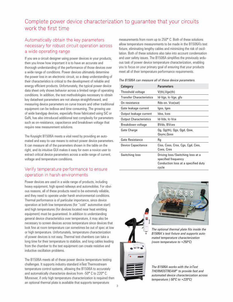
The B1506A meets all of these power device temperature testing
challenges. It supports industry-standard inTest Thermostream
temperature control systems, allowing the B1506A to accurately
and automatically characterize devices from -50° C to 220° C.
Moreover, if only high temperature characterization is required then
an optional thermal plate is available that supports temperature
measurements from room up to 250° C. Both of these solutions
allow temperature measurements to be made in the B1506A’s test
fixture, eliminating lengthy cables and minimizing the risk of oscil-
lation. Both of these solutions also take into account condensation
and user safety issues. The B1506A simplifies the previously ardu-
ous task of power device temperature characterization, enabling
you to focus on your primary goal of ensuring that your products
meet all of their temperature performance requirements.
Category Parameters
Threshold voltage V(th),Vge(th)
Transfer Characteristics Id-Vgs, Ic-Vge, gfs
On resistance Rds-on. Vce(sat)
Gate leakage current Igss, Iges
Output leakage current Idss, Ices
Output Characteristics Id-Vds, Ic-Vce
Breakdown voltage BVds, BVces
Gate Charge Qg, Qg(th), Qgs, Qgd, Qsw,
Qsync,Qoss
Gate Resistance Rg
Device Capacitance Ciss, Coss, Crss, Cgs, Cgd, Cies,
Coes, Cres
Switching loss Driving loss/Switching loss at a
specified frequency
Conduction loss at a specified duty
cycle
The optional thermal plate fits inside the
B1506A’s test fixture and supports auto-
mated temperature characterization
(room temperature to +250ºC)
The B1506A works with the inTest
THERMOSTREAM® to provide fast and
automated device characterization across
temperature (-50ºC to +220ºC)
4
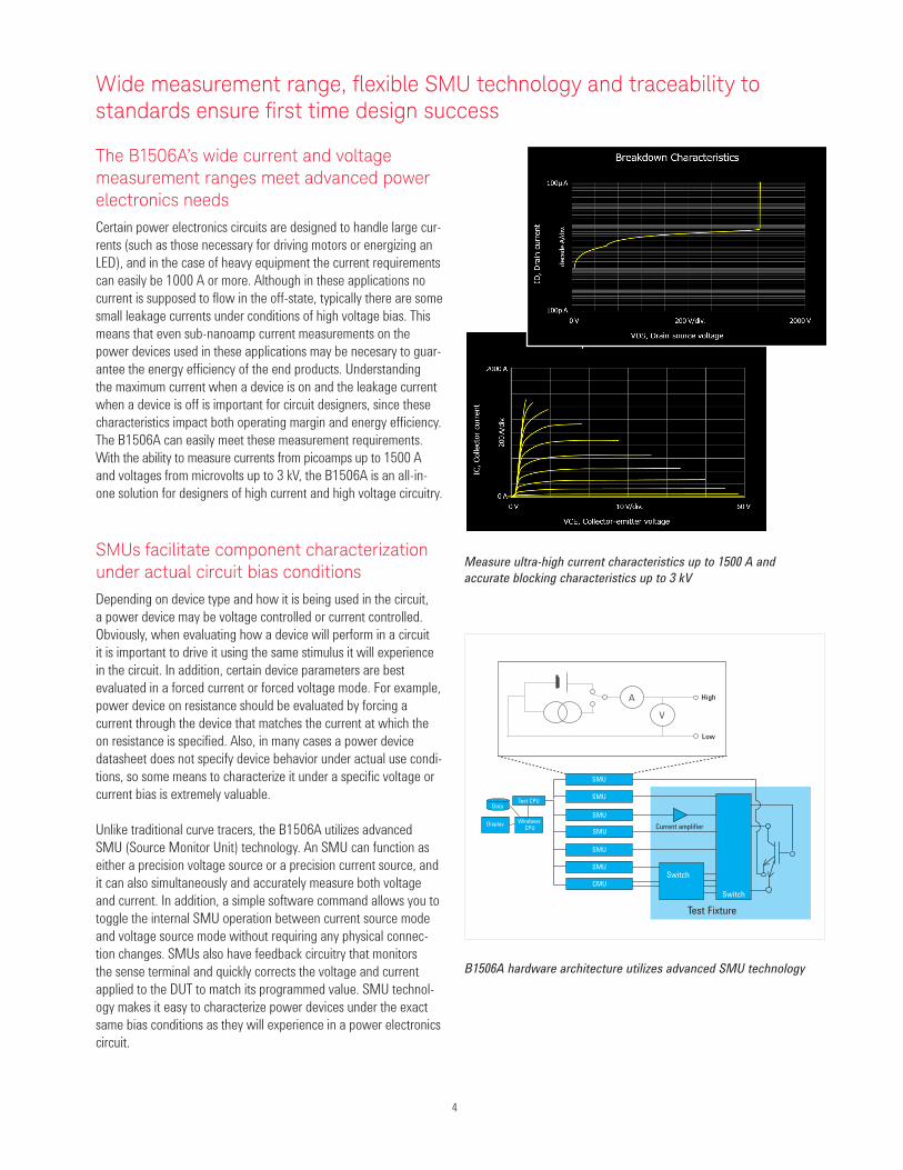
Measure ultra-high current characteristics up to 1500 A and
accurate blocking characteristics up to 3 kV
Wide measurement range, lexible SMU technology and traceability to standards ensure irst time design success
The B1506A’s wide current and voltage measurement ranges meet advanced power electronics needs
Certain power electronics circuits are designed to handle large cur-
rents (such as those necessary for driving motors or energizing an
LED), and in the case of heavy equipment the current requirements
can easily be 1000 A or more. Although in these applications no
current is supposed to flow in the off-state, typically there are some
small leakage currents under conditions of high voltage bias. This
means that even sub-nanoamp current measurements on the
power devices used in these applications may be necesary to guar-
antee the energy efficiency of the end products. Understanding
the maximum current when a device is on and the leakage current
when a device is off is important for circuit designers, since these
characteristics impact both operating margin and energy efficiency.
The B1506A can easily meet these measurement requirements.
With the ability to measure currents from picoamps up to 1500 A
and voltages from microvolts up to 3 kV, the B1506A is an all-in-
one solution for designers of high current and high voltage circuitry.
SMUs facilitate component characterization under actual circuit bias conditions
Depending on device type and how it is being used in the circuit,
a power device may be voltage controlled or current controlled.
Obviously, when evaluating how a device will perform in a circuit
it is important to drive it using the same stimulus it will experience
in the circuit. In addition, certain device parameters are best
evaluated in a forced current or forced voltage mode. For example,
power device on resistance should be evaluated by forcing a
current through the device that matches the current at which the
on resistance is specified. Also, in many cases a power device
datasheet does not specify device behavior under actual use condi-
tions, so some means to characterize it under a specific voltage or
current bias is extremely valuable.
Unlike traditional curve tracers, the B1506A utilizes advanced
SMU (Source Monitor Unit) technology. An SMU can function as
either a precision voltage source or a precision current source, and
it can also simultaneously and accurately measure both voltage
and current. In addition, a simple software command allows you to
toggle the internal SMU operation between current source mode
and voltage source mode without requiring any physical connec-
tion changes. SMUs also have feedback circuitry that monitors
the sense terminal and quickly corrects the voltage and current
applied to the DUT to match its programmed value. SMU technol-
ogy makes it easy to characterize power devices under the exact
same bias conditions as they will experience in a power electronics
circuit.
Switch
Switch
Current amplifier
Test Fixture
CMU
SMU
SMU
SMU
SMU
SMU
SMU
Windows CPU
Display
Test CPUData
A
V
Low
High
B1506A hardware architecture utilizes advanced SMU technology
5
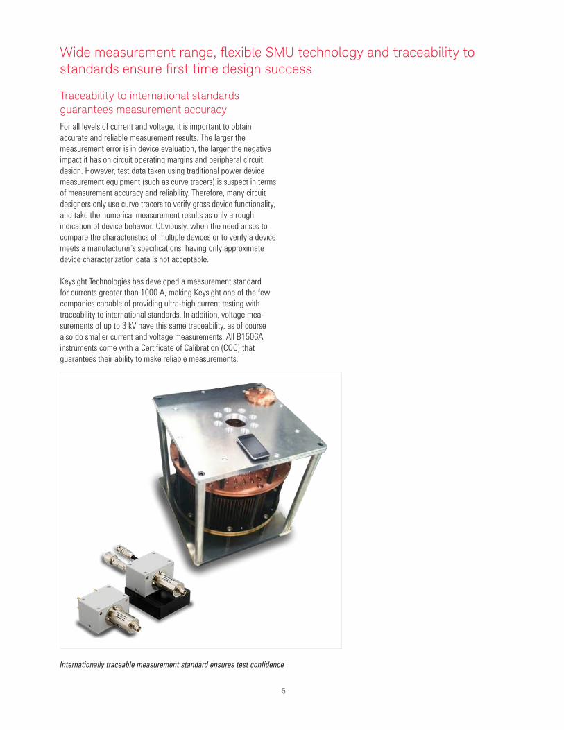
Traceability to international standards guarantees measurement accuracy
For all levels of current and voltage, it is important to obtain
accurate and reliable measurement results. The larger the
measurement error is in device evaluation, the larger the negative
impact it has on circuit operating margins and peripheral circuit
design. However, test data taken using traditional power device
measurement equipment (such as curve tracers) is suspect in terms
of measurement accuracy and reliability. Therefore, many circuit
designers only use curve tracers to verify gross device functionality,
and take the numerical measurement results as only a rough
indication of device behavior. Obviously, when the need arises to
compare the characteristics of multiple devices or to verify a device
meets a manufacturer’s specifications, having only approximate
device characterization data is not acceptable.
Keysight Technologies has developed a measurement standard
for currents greater than 1000 A, making Keysight one of the few
companies capable of providing ultra-high current testing with
traceability to international standards. In addition, voltage mea-
surements of up to 3 kV have this same traceability, as of course
also do smaller current and voltage measurements. All B1506A
instruments come with a Certificate of Calibration (COC) that
guarantees their ability to make reliable measurements.
Internationally traceable measurement standard ensures test confidence
Wide measurement range, lexible SMU technology and traceability to standards ensure irst time design success
6
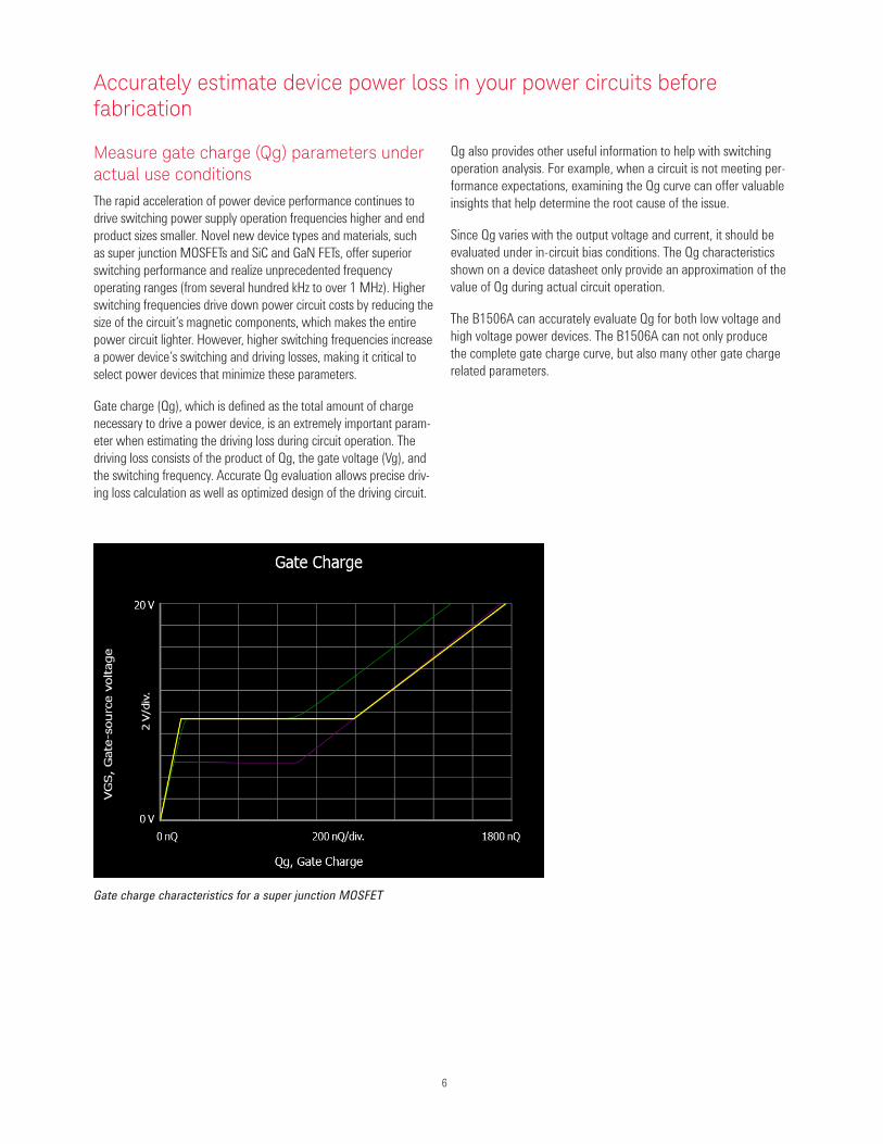
Gate charge characteristics for a super junction MOSFET
Accurately estimate device power loss in your power circuits before fabrication
Measure gate charge (Qg) parameters under actual use conditions
The rapid acceleration of power device performance continues to
drive switching power supply operation frequencies higher and end
product sizes smaller. Novel new device types and materials, such
as super junction MOSFETs and SiC and GaN FETs, offer superior
switching performance and realize unprecedented frequency
operating ranges (from several hundred kHz to over 1 MHz). Higher
switching frequencies drive down power circuit costs by reducing the
size of the circuit’s magnetic components, which makes the entire
power circuit lighter. However, higher switching frequencies increase
a power device’s switching and driving losses, making it critical to
select power devices that minimize these parameters.
Gate charge (Qg), which is defined as the total amount of charge
necessary to drive a power device, is an extremely important param-
eter when estimating the driving loss during circuit operation. The
driving loss consists of the product of Qg, the gate voltage (Vg), and
the switching frequency. Accurate Qg evaluation allows precise driv-
ing loss calculation as well as optimized design of the driving circuit.
Qg also provides other useful information to help with switching
operation analysis. For example, when a circuit is not meeting per-
formance expectations, examining the Qg curve can offer valuable
insights that help determine the root cause of the issue.
Since Qg varies with the output voltage and current, it should be
evaluated under in-circuit bias conditions. The Qg characteristics
shown on a device datasheet only provide an approximation of the
value of Qg during actual circuit operation.
The B1506A can accurately evaluate Qg for both low voltage and
high voltage power devices. The B1506A can not only produce
the complete gate charge curve, but also many other gate charge
related parameters.
7
Accurately estimate device power loss in your power circuits before fabrication
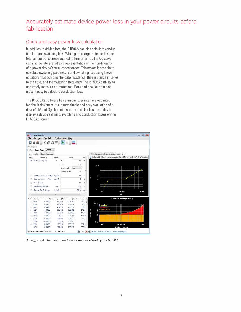
Quick and easy power loss calculationIn addition to driving loss, the B1506A can also calculate conduc-
tion loss and switching loss. While gate charge is defined as the
total amount of charge required to turn on a FET, the Qg curve
can also be interpreted as a representation of the non-linearity
of a power device’s stray capacitances. This makes it possible to
calculate switching parameters and switching loss using known
equations that combine the gate resistance, the resistance in series
to the gate, and the switching frequency. The B1506A’s ability to
accurately measure on-resistance (Ron) and peak current also
make it easy to calculate conduction loss.
The B1506A’s software has a unique user interface optimized
for circuit designers. It supports simple and easy evaluation of a
device’s IV and Qg characteristics, and it also has the ability to
display a device’s driving, switching and conduction losses on the
B1506A’s screen.
Driving, conduction and switching losses calculated by the B1506A
8
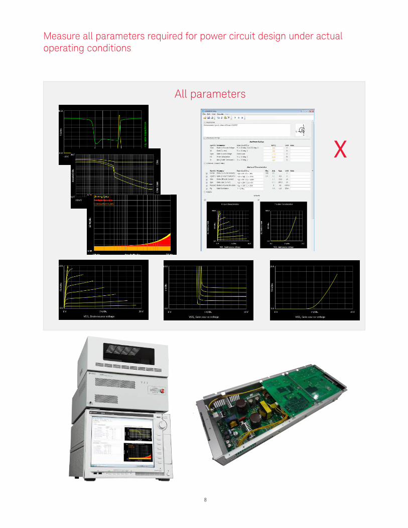
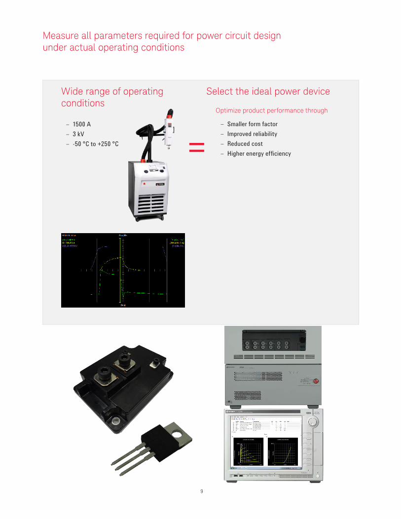
Measure all parameters required for power circuit design under actual operating conditions
X
All parameters
9
Measure all parameters required for power circuit design under actual operating conditions
Wide range of operating conditions
Select the ideal power device
=
Optimize product performance through
– Smaller form factor
– Improved reliability
– Reduced cost
– Higher energy efficiency
– 1500 A
– 3 kV
– -50 °C to +250 °C
10
Capacitance selector supports fully automated Ciss, Coss and Crss measurement
Easy and elegant switching loss analysis
Fully automated input, output and reverse transfer capacitance measurement
Understanding the input, output and reverse return capacitances
of three terminal devices (such as MOSFETs or IGBTs) is very
important, because these parameters dictate the switching speed
and the switching loss when a switching power supply operates at
high frequency. However, accurately measuring these parameters
is not easy or straightforward. When measuring the capacitance
between two terminals of a three terminal device, the other
terminal needs to be appropriately configured (using the capaci-
tance meter’s AC guard output) in order to make an accurate
measurement. Depending upon the capacitance parameter and
type of device being measured, other components (such as an AC
blocking resistor or a DC blocking capacitor) may also be needed.
In addition, some capacitance measurements need high voltage
biases to be applied to the DUT, requiring additional components
to protect instrument resources from damage in the event of
device breakdown. For all of these reasons, a great deal of skill
and thought needs to go into making a single type of capacitance
measurement, and it is easy to make a mistake that leads to invalid
data collection.
The B1506A can automatically and accurately measure FET
capacitance values (Ciss, Coss, Crss) using its built-in capacitance
selector module. The capacitance selector contains all of the
resistors, capacitors and protection circuits necessary to make
high-voltage capacitance measurements, and it automatically
arranges these components into the correct configuration for a
specified capacitance measurement. The B1506A’s capacitance
selector can even provide accurate capacitance data for normally
on devices (such as SiC JFETs).
Device capacitance selector
– Switch
– AC blocking R
– DC blocking C
D
S
G
HVSMU
MFCMU
11
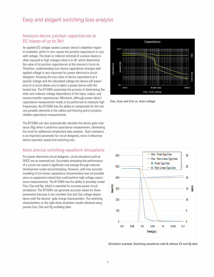
Ciss, Coss and Crss vs. drain voltage.
Easy and elegant switching loss analysis
Measure device junction capacitances at DC biases of up to 3kV
An applied DC voltage causes a power device’s depletion region
to modulate, which in-turn causes the junction capacitance to vary
with voltage. The drain or collector terminal of a power device is
often exposed to high voltages when it is off, which determines
the value of its junction capacitances at the moment it turns on.
Therefore, understanding how device capacitance changes with
applied voltage is very important for power electronics circuit
designers. Knowing the true value of device capacitance at a
specific voltage and the calculated voltage the device will experi-
ence in a circuit allows you to select a power device with the
lowest loss. The B1506A automates the process of determining the
drain and collector voltage dependency of the input, output, and
reverse transfer capacitances. Moreover, although power device
capacitance measurement needs to be performed at relatively high
frequencies, the B1506A has the ability to compensate for the vari-
ous parasitic elements in the cables and fixturing and to produce
reliable capacitance measurements.
The B1506A can also automatically calculate the device gate resis-
tance (Rg) when it performs capacitance measurement, eliminating
the need for additional complicated data analysis. Gate resistance
is an important parameter for circuit designers, since it influences
device operation speed and switching loss.
More precise switching waveform simulationsFor power electronics circuit designers, circuit simulators such as
SPICE are an essential tool. Accurately simulating the performance
of a circuit can result in significant cost savings through reduced
development cycles and prototyping. However, until now accurate
modeling of non-linear capacitance characteristics was not possible
since no equipment existed that could perform high voltage capaci-
tance measurements. The B1506A has the ability to precisely model
Crss, Ciss and Rg, which is essential for accurate power circuit
simulations. The B1506A can generate accurate values for these
parameters because it can correlate Crss and Ciss voltage depen-
dency with the devices’ gate charge characteristics. The switching
characteristics on the right show simulation results obtained using
precise Crss, Ciss and Rg modeling data.
Simulation example: Switching waveforms with & without CV and Rg data
12
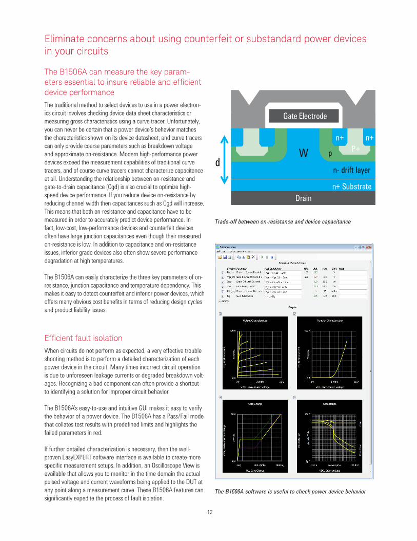
Trade-off between on-resistance and device capacitance
Eliminate concerns about using counterfeit or substandard power devices in your circuits
The B1506A can measure the key param-eters essential to insure reliable and eficient device performance
The traditional method to select devices to use in a power electron-
ics circuit involves checking device data sheet characteristics or
measuring gross characteristics using a curve tracer. Unfortunately,
you can never be certain that a power device’s behavior matches
the characteristics shown on its device datasheet, and curve tracers
can only provide coarse parameters such as breakdown voltage
and approximate on-resistance. Modern high-performance power
devices exceed the measurement capabilities of traditional curve
tracers, and of course curve tracers cannot characterize capacitance
at all. Understanding the relationship between on-resistance and
gate-to-drain capacitance (Cgd) is also crucial to optimize high-
speed device performance. If you reduce device on-resistance by
reducing channel width then capacitances such as Cgd will increase.
This means that both on-resistance and capacitance have to be
measured in order to accurately predict device performance. In
fact, low-cost, low-performance devices and counterfeit devices
often have large junction capacitances even though their measured
on-resistance is low. In addition to capacitance and on-resistance
issues, inferior grade devices also often show severe performance
degradation at high temperatures.
The B1506A can easily characterize the three key parameters of on-
resistance, junction capacitance and temperature dependency. This
makes it easy to detect counterfeit and inferior power devices, which
offers many obvious cost benefits in terms of reducing design cycles
and product liability issues.
Eficient fault isolation
When circuits do not perform as expected, a very effective trouble
shooting method is to perform a detailed characterization of each
power device in the circuit. Many times incorrect circuit operation
is due to unforeseen leakage currents or degraded breakdown volt-
ages. Recognizing a bad component can often provide a shortcut
to identifying a solution for improper circuit behavior.
The B1506A’s easy-to-use and intuitive GUI makes it easy to verify
the behavior of a power device. The B1506A has a Pass/Fail mode
that collates test results with predefined limits and highlights the
failed parameters in red.
If further detailed characterization is necessary, then the well-
proven EasyEXPERT software interface is available to create more
specific measurement setups. In addition, an Oscilloscope View is
available that allows you to monitor in the time domain the actual
pulsed voltage and current waveforms being applied to the DUT at
any point along a measurement curve. These B1506A features can
significantly expedite the process of fault isolation.
Drain
n+ Substrate
n- drift layer
Source
Wd
n+ n+
p
Gate Electrode
P+
n+
Drain
The B1506A software is useful to check power device behavior

13
The intuitive data sheet characterization mode provides complete
device characteristics in a few simple steps
Achieve accurate results immediately without the need for training or mea-surement expertise
Intuitive data sheet style user interface and simple cable connections eliminate need for product training
Traditional power device evaluation has been a complicated
process involving many different pieces of equipment (curve tracers,
oscilloscopes, LCR meters, production functional testers, etc.). Not
only does it take a long time to learn how to use this equipment
properly, but a lack of automation capability means that it is easy
to make mistakes that can cast doubt on the measurement results.
However, the B1506A has a unique data sheet characterization
mode that displays device tests in data sheet format. It provides
an intuitive interface that enables anyone to measure key device
parameters without any specialized training. In addition, all device
characteristics (including high current, high voltage, small leakage
currents and three terminal device capacitances) can be measured
without any need to modify the device connections. Since typical test
setups for common devices such as MOSFET and IGBTs are built-in,
you can start characterizing devices immediately after unpacking
the B1506A. Of course, it is also easy to customize the predefined
setups. All measurement results are automatically stored onto
the B1506A’s internal hard disk drive, making it easy to generate
test reports later. To facilitate the detection of counterfeit and
substandard devices quickly, a Pass/Fail feature is also available.
The B1506A’s cabling connections and DUT connections inside
the test fixture are also easy to make, and the B1506A’s simplified
interface architecture greatly minimizes the chance of operator error.
From both a hardware and software perspective, the B1506A is the
best instrument to perform power device characterization.
Innovative switching technology supports a fully automated IV and CV measurement solution
Although understanding both the IV and CV characteristics of power
devices has become more important than ever as switching frequen-
cies have increased, no equipment has been available that could
evaluate both of these parameters. There are several reasons for this,
all relating to the CV measurements. The first is simply that high volt-
age bias CV measurements are innately difficult to make. The second
is that the circuit complexities involved in switching between IV and
CV measurements are not trivial, since some capacitance measure-
ments require additional AC or DC blocking components. The third
and final issue is that CV measurements require proper compensation
to cancel out measurement error, which typically requires some
measurement expertise on the part of the user. In addition to these
challenges, automating this entire process is not a trivial task.
However, Keysight’s unmatched semiconductor device capacitance
measurement expertise, combined with an innovative switching solu-
tion, allows the B1506A to make fully compensated and automatic IV
and CV measurements at the touch of a button.
4. Execute
1. Edit conditions
3. Select parameters to measure
2. Edit range
Simplified DUT connections eliminate errors
Innovative switching solution supports fully automated IV and CV
measurements
D
S
G
Main
fram
e DC Switches
Device
capacitance
selector
Sw
itches
14
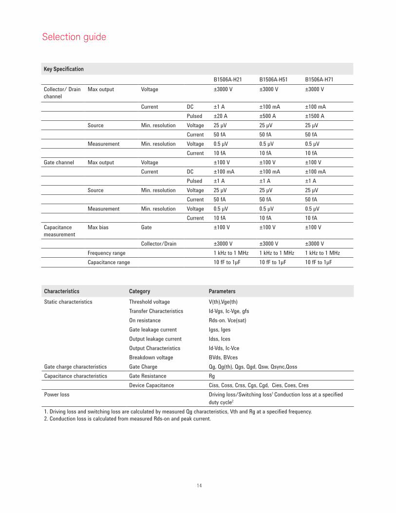
Selection guide
Key Speciication
B1 5 0 6 A-H2 1 B1 5 0 6 A-H5 1 B1 5 0 6 A-H7 1
Collector/ Drain
channel
Max output Voltage ±3000 V ±3000 V ±3000 V
Current DC ±1 A ±100 mA ±100 mA
Pulsed ±20 A ±500 A ±1500 A
Source Min. resolution Voltage 25 µV 25 µV 25 µV
Current 50 fA 50 fA 50 fA
Measurement Min. resolution Voltage 0.5 µV 0.5 µV 0.5 µV
Current 10 fA 10 fA 10 fA
Gate channel Max output Voltage ±100 V ±100 V ±100 V
Current DC ±100 mA ±100 mA ±100 mA
Pulsed ±1 A ±1 A ±1 A
Source Min. resolution Voltage 25 µV 25 µV 25 µV
Current 50 fA 50 fA 50 fA
Measurement Min. resolution Voltage 0.5 µV 0.5 µV 0.5 µV
Current 10 fA 10 fA 10 fA
Capacitance
measurement
Max bias Gate ±100 V ±100 V ±100 V
Collector/Drain ±3000 V ±3000 V ±3000 V
Frequency range 1 kHz to 1 MHz 1 kHz to 1 MHz 1 kHz to 1 MHz
Capacitance range 10 fF to 1µF 10 fF to 1µF 10 fF to 1µF
Characteristics Category Parameters
Static characteristics Threshold voltage V(th),Vge(th)
Transfer Characteristics Id-Vgs, Ic-Vge, gfs
On resistance Rds-on. Vce(sat)
Gate leakage current Igss, Iges
Output leakage current Idss, Ices
Output Characteristics Id-Vds, Ic-Vce
Breakdown voltage BVds, BVces
Gate charge characteristics Gate Charge Qg, Qg(th), Qgs, Qgd, Qsw, Qsync,Qoss
Capacitance characteristics Gate Resistance Rg
Device Capacitance Ciss, Coss, Crss, Cgs, Cgd, Cies, Coes, Cres
Power loss Driving loss/Switching loss1 Conduction loss at a specified
duty cycle2
1. Driving loss and switching loss are calculated by measured Qg characteristics, Vth and Rg at a specified frequency.
2. Conduction loss is calculated from measured Rds-on and peak current.
15
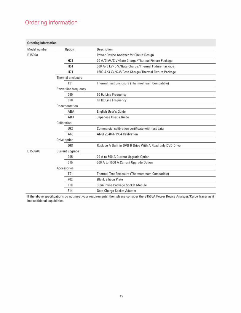
Ordering information
Ordering Information
Model number Option Description
B1506A Power Device Analyzer for Circuit Design
H21 20 A/3 kV/C-V/Gate Charge/Thermal Fixture Package
H51 500 A/3 kV/C-V/Gate Charge/Thermal Fixture Package
H71 1500 A/3 kV/C-V/Gate Charge/Thermal Fixture Package
Thermal enclosure
T01 Thermal Test Enclosure (Thermostream Compatible)
Power line frequency
050 50 Hz Line Frequency
060 60 Hz Line Frequency
Documentation
ABA English User's Guide
ABJ Japanese User's Guide
Calibration
UK6 Commercial calibration certificate with test data
A6J ANSI Z540-1-1994 Calibration
Drive option
DR1 Replace A Built-in DVD-R Drive With A Read-only DVD Drive
B1506AU Current upgrade
005 20 A to 500 A Current Upgrade Option
015 500 A to 1500 A Current Upgrade Option
Accessories
T01 Thermal Test Enclosure (Thermostream Compatible)
F02 Blank Silicon Plate
F10 3-pin Inline Package Socket Module
F14 Gate Charge Socket Adapter
If the above specifications do not meet your requirements, then please consider the B1505A Power Device Analyzer/Curve Tracer as it
has additional capabilities.

myKeysight
www.keysight.com/find/mykeysight
A personalized view into the information most relevant to you.
Three-Year Warranty
www.keysight.com/find/ThreeYearWarranty
Keysight’s commitment to superior product quality and lower total cost of ownership. The only test and measurement company with three-year
warranty standard on all instruments, worldwide.
Keysight Assurance Plans
www.keysight.com/find/AssurancePlans
Up to five years of protection and no budgetary surprises to ensure your instruments are operating to specification so you can rely on accurate
measurements.
www.keysight.com/go/quality
Keysight Technologies, Inc.
DEKRA Certified ISO 9001:2008 Quality Management System
Keysight Channel Partners
www.keysight.com/find/channelpartners
Get the best of both worlds: Keysight’s measurement expertise and product breadth, combined with channel partner convenience.
www.keysight.com/find/b1506a
For more information on Keysight
Technologies’ products, applications or
services, please contact your local Keysight
office. The complete list is available at:www.keysight.com/find/contactus
Americas
Canada (877) 894 4414Brazil 55 11 3351 7010Mexico 001 800 254 2440United States (800) 829 4444
Asia PaciicAustralia 1 800 629 485China 800 810 0189Hong Kong 800 938 693India 1 800 112 929Japan 0120 (421) 345Korea 080 769 0800Malaysia 1 800 888 848Singapore 1 800 375 8100Taiwan 0800 047 866Other AP Countries (65) 6375 8100
Europe & Middle EastAustria 0800 001122Belgium 0800 58580Finland 0800 523252France 0805 980333Germany 0800 6270999Ireland 1800 832700Israel 1 809 343051Italy 800 599100Luxembourg +32 800 58580Netherlands 0800 0233200Russia 8800 5009286Spain 0800 000154Sweden 0200 882255Switzerland 0800 805353
Opt. 1 (DE)Opt. 2 (FR)Opt. 3 (IT)
United Kingdom 0800 0260637
For other unlisted countries:www.keysight.com/find/contactus
(BP-09-04-14)
16 | Keysight | B1506A Power Device Analyzer for Circuit Design
This information is subject to change without notice.© Keysight Technologies, 2014Published in USA, July 3, 20145991-4279ENwww.keysight.com
Keysight B2900 Precision
Instrument Family
www.keysight.com/find/b2900a
Keysight B1500A Semiconductor
Device Analyzer
www.keysight.com/find/b1500a
Keysight B1505A Power
Device Analyzer/Curve Tracer
(1500 A/10 kV)www.keysight.com/find/b1505a